

Philips PCA3351CH, PCA3351CP, PCA3351CT, PCA3352CH, PCA3352CP Datasheet
...
DATA SH EET
Product specification
Supersedes data of 1996 Dec 18
File under Integrated Circuits, IC03
1999 Oct 28
INTEGRATED CIRCUITS
PCA3351C; 52C; 53C;
PCD3351A; 52A; 53A
8-bit microcontrollers with DTMF
generator and 128 bytes EEPROM

1999 Oct 28 2
Philips Semiconductors Product specification
8-bit microcontrollers with DTMF generator
and 128 bytes EEPROM
PCA3351C; 52C; 53C;
PCD3351A; 52A; 53A
CONTENTS
1 FEATURES
2 GENERAL DESCRIPTION
3 ORDERING INFORMATION
4 BLOCK DIAGRAM
5 PINNING INFORMATION
5.1 Pinning
5.2 Pin description
6 FREQUENCY GENERATOR
6.1 Frequency generator derivative registers
6.2 Melody output (P1.7/MDY)
6.3 Frequency registers
6.4 DTMF frequencies
6.5 Modem frequencies
6.6 Musical scale frequencies
7 EEPROM AND TIMER 2 ORGANIZATION
7.1 EEPROM registers
7.2 EEPROM latches
7.3 EEPROM flags
7.4 EEPROM macros
7.5 EEPROM access
7.6 Timer 2
8 DERIVATIVE INTERRUPTS
9 TIMING
10 RESET
11 IDLE MODE
12 STOP MODE
13 INSTRUCTION SET RESTRICTIONS
14 OVERVIEW OF PORT AND
POWER-ON-RESET CONFIGURATIONS
15 SUMMARY OF DERIVATIVE REGISTERS
16 HANDLING
17 LIMITING VALUES
18 DC CHARACTERISTICS
19 AC CHARACTERISTICS
20 PACKAGE OUTLINES
21 SOLDERING
21.1 Reflow soldering
21.2 Wave soldering
21.3 DIP
21.4 Repairing soldered joints
22 DEFINITIONS
23 LIFE SUPPORT APPLICATIONS
1999 Oct 28 3
Philips Semiconductors Product specification
8-bit microcontrollers with DTMF generator
and 128 bytes EEPROM
PCA3351C; 52C; 53C;
PCD3351A; 52A; 53A
1 FEATURES
• 8-bit CPU, ROM, RAM, EEPROM and I/O; all in one
(28-lead or 32-lead) package
• ROM:
– 2 kbytes (PCA3351C and PCD3351A)
– 4 kbytes (PCA3352C and PCD3352A)
– 6 kbytes (PCA3353C and PCD3353A)
• RAM:
– 64 bytes (PCA3351C and PCD3351A)
– 128 bytes (PCA3352C, PCD3352A, PCA3353C and
PCD3353A)
• 128 bytes Electrically Erasable Programmable
Read-Only Memory (EEPROM)
• Over 100 instructions (based on MAB8048) all of
1 or 2 cycles
• 20 quasi-bidirectional I/O port lines
• 8-bit programmable Timer/event counter 1
• 8-bit reloadable Timer 2
• Three single-level vectored interrupts:
– external
– 8-bit programmable Timer/event counter 1
– derivative; triggered by reloadable Timer 2
• Twotestinputs,oneofwhichalsoservesastheexternal
interrupt input
• DTMF, modem, musical tone generator
• Reference for supply and temperature-independent
tone output
• Filtering for low output distortion (CEPT compatible)
• Melody output for ringer application
• Power-on-reset
• Stop and Idle modes
• Supply voltage: 1.8 to 6 V (DTMF tone output and
EEPROM erase/write from 2.5 V)
• Clock frequency: 1 to 16 MHz (3.58 MHz for DTMF
suggested)
• Operating ambient temperature: −25 to +70 °C or
0to50°C
• Manufactured in silicon gate CMOS process.
2 GENERAL DESCRIPTION
This data sheet details the specific properties of the
devices referred to. The shared properties of the
PCD33xxA family of microcontrollers are described in the
“PCD33xxA family”
data sheet, which should be read in
conjunction with this publication.
• ‘PCA3351C; 52C; 53C’ denotes the types PCA3351C,
PCA3352C and PCA3353C. Unless specified, these
types will hereafter be referred to collectively as
‘PCA335xC’.
• ‘PCD3351A; 52A; 53A’ denotes the types PCD3351A,
PCD3352A, PCD3353A. Unless specified, these types
will hereafter be referred to collectively as ‘PCD335xA’.
The PCA335xC and PCD335xA are microcontrollers
designed primarily for telephony applications. They
include an on-chip generator for dual tone multifrequency
(DTMF), modem and musical tones. In addition to dialling,
generated frequencies can be made available as square
waves for melody generation, providing ringer operation.
The PCA335xC and PCD335xA also incorporate
128 bytes of EEPROM, permitting data storage without
battery backup. The EEPROM can be used for storing
telephone numbers, particularly for implementing redial
functions.
The PCA335xC and PCD335xA can be emulated with the
OTP microcontrollers PCD3755A and PCD3755E.
See Chapter 14, Table 25.
The instruction set is similar to that of the MAB8048 and is
a sub-set of that listed in the
“PCD33xxA family”
data
sheet.
The differences between PCA335xC and PCD335xA are
shown in Table 1.
Table 1 Differences: PCA335xC and PCD335xA
Note
1. See Chapter 14, Table 26.
TYPE V
POR
AMBIENT
TEMP. RANGE
PCA335xC fixed at 2.0 V ±0.3 V 0 to 50 °C
PCD335xA (1.2 to 3.6 V) ±0.5 V
(1)
−25 to +70 °C
1999 Oct 28 4
Philips Semiconductors Product specification
8-bit microcontrollers with DTMF generator
and 128 bytes EEPROM
PCA3351C; 52C; 53C;
PCD3351A; 52A; 53A
3 ORDERING INFORMATION
Note
1. The types:
a) PCA335xC denotes: PCA3351C, PCA3352C or PCA3353C.
b) PCD335xA denotes: PCD3351A, PCD3352A or PCD3353A.
TYPE
NUMBER
(1)
PACKAGE
NAME DESCRIPTION VERSION
PCA335xCP DIP28 plastic dual in-line package; 28 leads (600 mil) SOT117-1
PCD335xAP
PCA335xCT SO28 plastic small outline package; 28 leads; body width 7.5 mm SOT136-1
PCD335xAT
PCA335xCH LQFP32 plastic low profile quad flat package; 32 leads; body 7 × 7 × 1.4 mm SOT358-1
PCD335xAH
1999 Oct 28 5
Philips Semiconductors Product specification
8-bit microcontrollers with DTMF generator
and 128 bytes EEPROM
PCA3351C; 52C; 53C;
PCD3351A; 52A; 53A
This text is here in white to force landscape pages to be rotated correctly when browsing through the pdf in the Acrobat reader.This text is here in
_white to force landscape pages to berotatedcorrectlywhen browsing through the pdf in the Acrobat reader.This text is here inThis text is here in
white to force landscape pages to be rotated correctly when browsing through the pdf in the Acrobat reader. white to force landscape pages to be ...
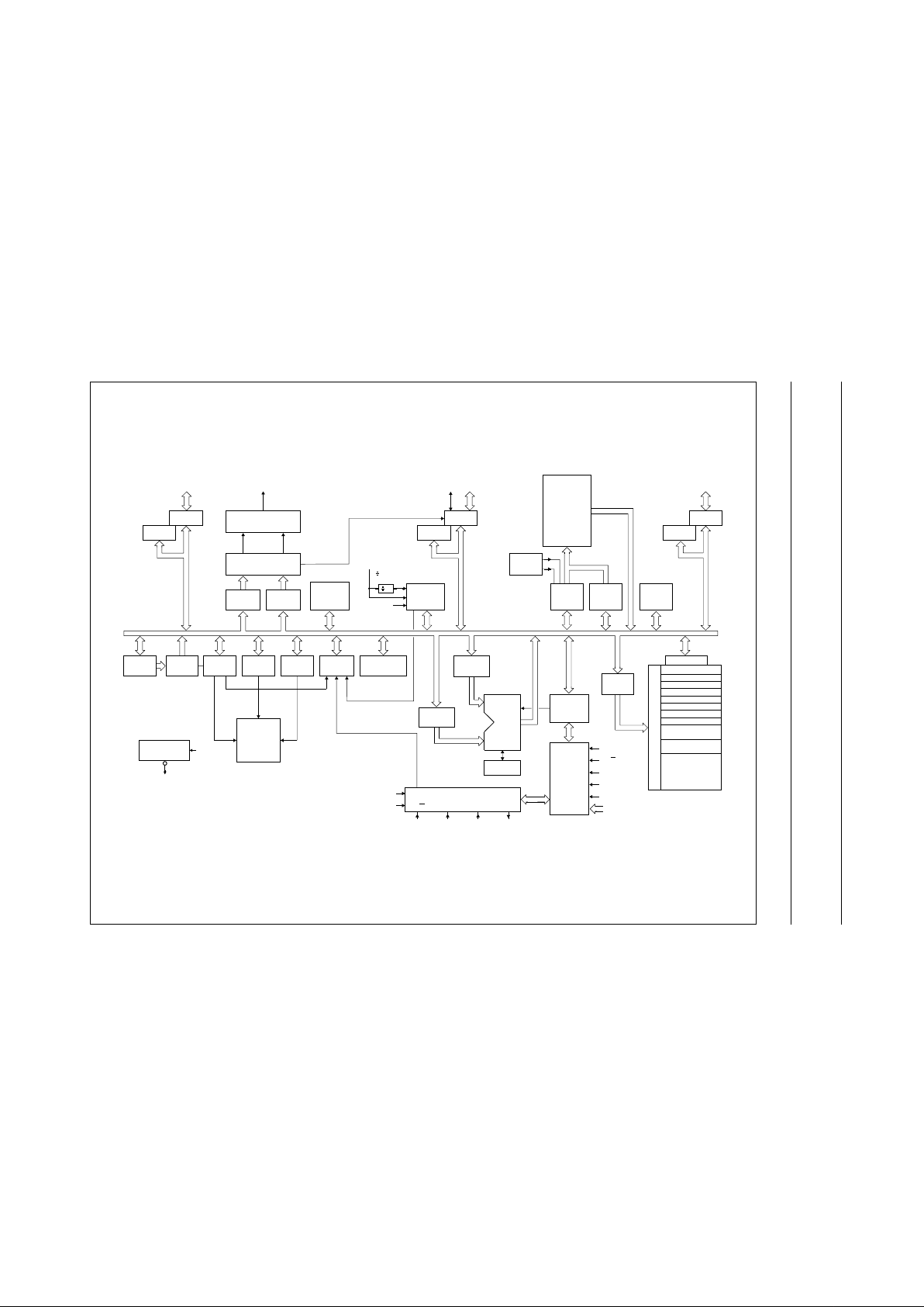
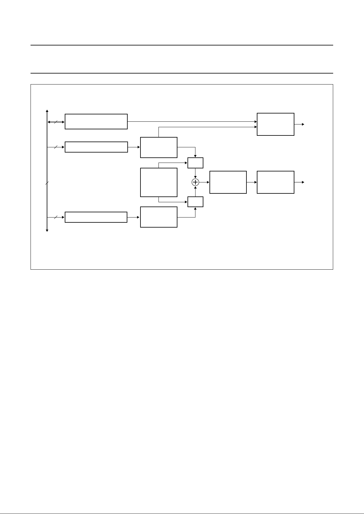
4 BLOCK DIAGRAM
handbook, full pagewidth
MLA537
PORT 0
FLIP-FLOP
PORT 0
BUFFER
HIGHER
PROGRAM
COUNTER
LOWER
PROGRAM
COUNTER
PROGRAM
STATUS
WORD
MEMORY
BANK
FLIP-FLOPS
6 kbytes
(PCD3353C; 53A)
4 kbytes
(PCD3352C; 52A)
2 kbytes
(PCD3351C; 51A)
128 bytes
(PCD3352C; 52A; 53C; 53A)
64 bytes
(PCD3351C; 51A)
DECODE
RESIDENT ROM
5888 8
P0.0 to P0.7
88
88
8
8
TIMER/
EVENT
COUNTER
32
INTERNAL
CLOCK
FREQ.
30
T1
PORT 1
BUFFER
PORT 1
FLIP-FLOP
P1.7/MDY P1.0 to P1.6
8
PORT 2
BUFFER
PORT 2
FLIP-FLOP
P2.0 to P2.3
4
4 7
8
MELODY
CONTROL
REGISTER
8
TONE
FILTER
OSCILLATOR
RAM
ADDRESS
REGISTER
ACCUMULATOR
TEMPORARY
REGISTER 1
TEMPORARY
REGISTER 2
ARITHMETIC
DECIMAL
ADJUST
CONTROL AND TIMING
XTAL2XTAL1RESET
CE/T0
STOP
IDLE
INTERRUPT INITIALIZE
MULTIPLEXER
8 LEVEL STACK
(VARIABLE LENGTH)
OPTIONAL SECOND
REGISTER BANK
DATA STORE
D
E
C
O
D
E
REGISTER 0
REGISTER 1
REGISTER 2
REGISTER 3
REGISTER 4
REGISTER 5
REGISTER 6
REGISTER 7
timer interrupt
external interrupt
RESIDENT RAM ARRAY
derivative
interrupt
8
LOGIC UNIT
8
INSTRUCTION
REGISTER
AND
DECODER
CONDITIONAL
BRANCH
LOGIC
CE/T0
TIMER
FLAG
CARRY
ACC
ACC BIT
TEST
T1
LGF
REGISTER
8
HGF
REGISTER
8
SINE WAVE
GENERATOR
INTERRUPT
LOGIC
8
EEPROM
DATA
TRANSFER
8
EEPROM
ADDRESS
REGISTER
8
EEPROM
CONTROL
REGISTER
8
TIMER 2
REGISTER
8
TIMER 2
RELOAD
REGISTER
8
EEPROM
PCA3351C
PCA3352C
PCA3353C
PCD3351A
PCD3352A
PCD3353A
POWER-ON-RESET
V
POR
RESET
Fig.1 Block diagram.
1999 Oct 28 6
Philips Semiconductors Product specification
8-bit microcontrollers with DTMF generator
and 128 bytes EEPROM
PCA3351C; 52C; 53C;
PCD3351A; 52A; 53A
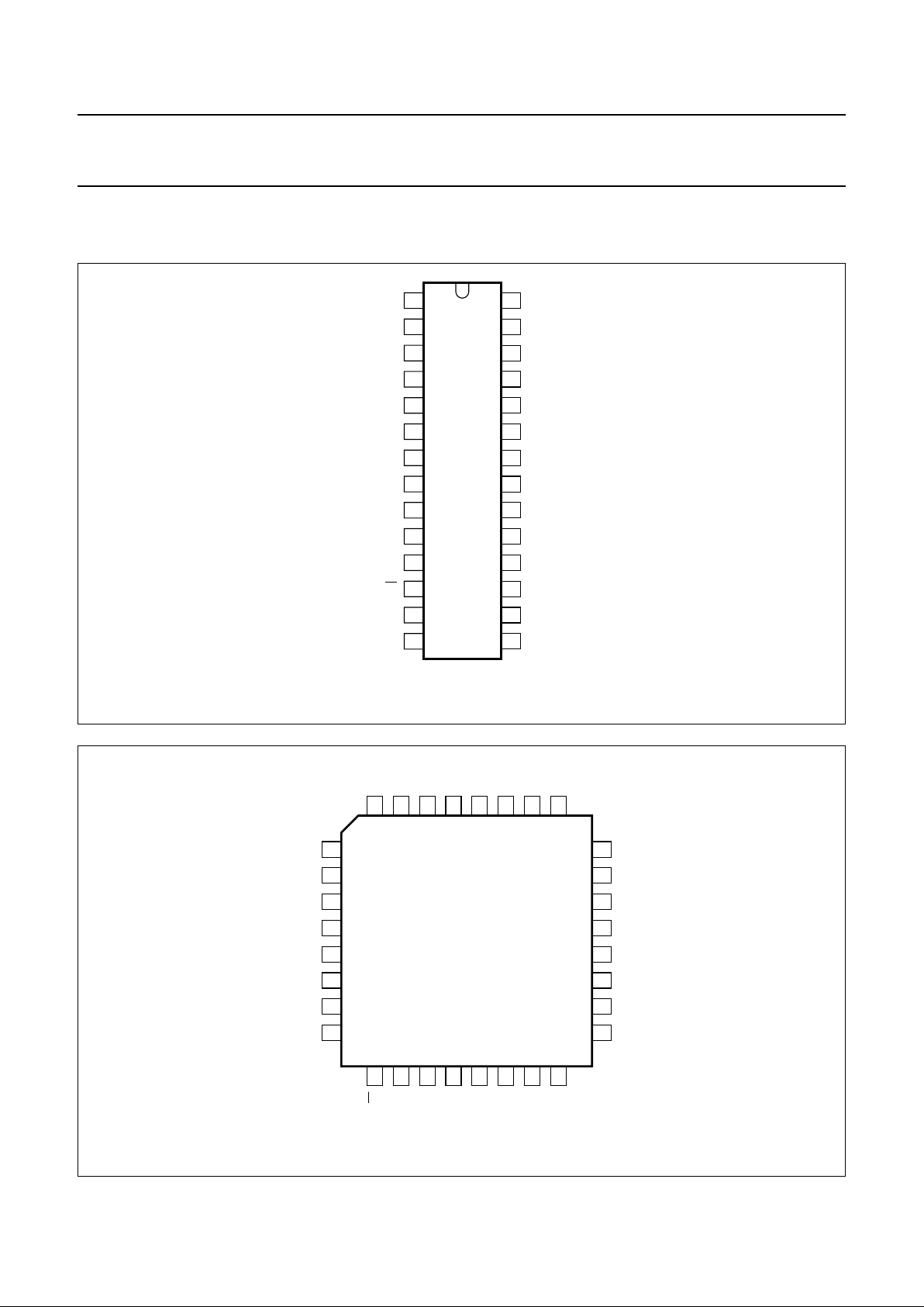
5 PINNING INFORMATION
5.1 Pinning
Fig.2 Pin configuration for DIP28 (SOT117-1) and SO28 (SOT136-1).
handbook, halfpage
1
2
3
4
5
6
7
8
9
10
11
12
13
28
27
26
25
24
23
22
21
20
19
18
17
16
1514
P0.1
P0.2
P0.3
P0.4
P0.5
P0.6
P0.7
T1
XTAL1
XTAL2
RESET
CE/T0
P1.0
P1.1
P0.0
P2.3
P2.2
P2.1
TONE
V
SS
V
DD
P2.0
P1.7/MDY
P1.6
P1.5
P1.4
P1.3
P1.2
PCA335xC
PCD335xA
(1)
MLA538
(1) PCA335xC denotes:
PCA3351C, PCA3352C or
PCA3353C.
PCD335xA denotes:
PCD3351A, PCD3352A or
PCD3353A.
Fig.3 Pin configuration for LQFP32 (SOT358-1).
handbook, full pagewidth
MGB795
1
2
3
4
5
6
7
8
24
23
22
21
20
19
18
17
9
10
11
12
13
14
15
16
32
31
30
29
28
27
26
25
n.c.
P0.5
P0.6
P0.7
T1
XTAL1
XTAL2
RESET
CE/T0
P1.0
P1.1
P1.2
P1.3
P1.4
P1.5
n.c.
P1.6
P2.0
P2.1
P2.2
P2.3
P0.0
n.c.
P0.1
P0.2
P0.3
P0.4
TONE
V
SS
V
DD
P1.7/MDY
n.c.
PCA335xCH
PCD335xAH
(1)
(1) PCA335xCH denotes:
PCA3351CH, PCA3352CH or
PCA3353CH.
PCD335xAH denotes:
PCD3351AH, PCD3352AH or
PCD3353AH.
1999 Oct 28 7
Philips Semiconductors Product specification
8-bit microcontrollers with DTMF generator
and 128 bytes EEPROM
PCA3351C; 52C; 53C;
PCD3351A; 52A; 53A
5.2 Pin description
Table 2 SOT117-1 and SOT136-1 packages (for information on parallel I/O ports, see Chapter 14)
Table 3 SOT358-1 package (for information on parallel I/O ports, see Chapter 14)
SYMBOL PIN TYPE DESCRIPTION
P0.1 to P0.7 1 to 7 I/O 7 bits of Port 0: 8-bit quasi-bidirectional I/O port
T1 8 I Test 1 or count input of 8-bit Timer/event counter 1
XTAL1 9 I crystal oscillator or external clock input
XTAL2 10 O crystal oscillator output
RESET 11 I reset input
CE/
T0 12 I Chip Enable or Test 0
P1.0 to P1.6 13 to 19 I/O 7 bits of Port 1: 8-bit quasi-bidirectional I/O port
P1.7/MDY 20 I/O 1 bit of Port 1: 8-bit quasi-bidirectional I/O port; or melody output
P2.0 21 I/O 1 bit of Port 2: 4-bit quasi-bidirectional I/O port
V
SS
22 P ground
TONE 23 O DTMF output
V
DD
24 P positive supply voltage
P2.1 to P2.3 25 to 27 I/O 3 bits of Port 2: 4-bit quasi-bidirectional I/O port
P0.0 28 I/O 1 bit of Port 0: 8-bit quasi-bidirectional I/O port
SYMBOL PIN TYPE DESCRIPTION
n.c. 1 − not connected
P0.5 to P0.7 2 to 4 I/O 3 bits of Port 0: 8-bit quasi-bidirectional I/O port
T1 5 I Test 1 or count input of 8-bit Timer/event counter 1
XTAL1 6 I crystal oscillator or external clock input
XTAL2 7 O crystal oscillator output
RESET 8 I reset input
CE/
T0 9 I Chip Enable or Test 0
P1.0 to P1.2 10 to 12 I/O 3 bits of Port 1: 8-bit quasi-bidirectional I/O port
n.c. 13 − not connected
P1.3 to P1.5 14 to 16 I/O 3 bits of Port 1: 8-bit quasi-bidirectional I/O port
n.c. 17 − not connected
P1.6 18 I/O 1 bit of Port 1: 8-bit quasi-bidirectional I/O port
P1.7/MDY 19 I/O 1 bit of Port 1: 8-bit quasi-bidirectional I/O port; or melody output
P2.0 20 I/O 1 bit of Port 2: 4-bit quasi-bidirectional I/O port
V
SS
21 P ground
TONE 22 O DTMF output
V
DD
23 P positive supply voltage
P2.1 to P2.3 24 to 26 I/O 3 bits of Port 2: 4-bit quasi-bidirectional I/O port
P0.0 27 I/O 1 bit of Port 0: 8-bit quasi-bidirectional I/O port
n.c. 28 − not connected
P0.1 to P0.4 29 to 32 I/O 4 bits of Port 0: 8-bit quasi-bidirectional I/O port
1999 Oct 28 8
Philips Semiconductors Product specification
8-bit microcontrollers with DTMF generator
and 128 bytes EEPROM
PCA3351C; 52C; 53C;
PCD3351A; 52A; 53A
6 FREQUENCY GENERATOR
A versatile frequency generator section is provided (see
Fig.4). For normal operation, use a 3.58 MHz quartz
crystal or PXE resonator. The frequency generator
includes precision circuitry for dual tone multifrequency
(DTMF) signals, which is typically used for tone dialling
telephone sets.
Theirfrequencies are provided in purely sinusoidalformon
the TONE output or as square waves on the port line
P1.7/MDY.
The TONE output can alternatively issue twelve modem
frequencies for data rates between 300 and 1200 bits/s.
In addition to DTMF and modem frequencies, two octaves
of musical scale in steps of semitones are available.
When no tones are generated the TONE output is in
3-state mode.
6.1 Frequency generator derivative registers
6.1.1 HIGH AND LOW GROUP FREQUENCY REGISTERS
Table 4 gives the addresses, symbols and access types of the High Group Frequency (HGF) and Low Group Frequency
(LGF) registers.
Table 4 Hexadecimal addresses, symbols, access types and bit symbols of the frequency registers
6.1.2 MELODY CONTROL REGISTER (MDYCON)
Table 5 Melody Control Register, MDYCON (address 13H; access type R/W)
Table 6 Description of MDYCON bits
REGISTER
ADDRESS
REGISTER
SYMBOL
ACCESS
TYPE
BIT SYMBOLS
7 6 5 4 3 2 1 0
11H HGF W H7H6H5H4H3H2H1H0
12H LGF W L7L6L5L4L3L2L1L0
7 6 5 4 3 2 1 0
0000000EMO
BIT SYMBOL DESCRIPTION
7to1 − These bits are set to a logic 0.
0 EMO Enable Melody Output. If bit EMO = 0, then P1.7/MDY is a standard port line.
If bit EMO = 1, then P1.7/MDY is the melody output. EMO = 1 does not inhibit the port
instructions for P1.7/MDY. Therefore the state of both port line and flip-flop may be read
in and the port flip-flop may be written by port instructions. However, the port flip-flop of
P1.7/MDY must remain set to avoid conflicts between melody and port outputs.
When the HGF contents are zero while EMO = 1, P1.7/MDY is in the HIGH state.
1999 Oct 28 9
Philips Semiconductors Product specification
8-bit microcontrollers with DTMF generator
and 128 bytes EEPROM
PCA3351C; 52C; 53C;
PCD3351A; 52A; 53A
Fig.4 Block diagram of the frequency generator and melody output (P1.7/MDY) section.
handbook, full pagewidth
MLC416
HGF REGISTER
MELODY CONTROL
REGISTER
LGF REGISTER
INTERNAL BUS
8
8
8
8
SWITCHED
CAPACITOR
BANDGAP
VOLTAGE
REFERENCE
DIGITAL
SINE WAVE
SYNTHESIZER
DIGITAL
SINE WAVE
SYNTHESIZER
SWITCHED
CAPACITOR
LOW-PASS
FILTER
DAC
DAC
RC LOW-PASS
FILTER
TONE
PORT/MELODY
OUTPUT LOGIC
P1.7/
MDY
square wave
1999 Oct 28 10
Philips Semiconductors Product specification
8-bit microcontrollers with DTMF generator
and 128 bytes EEPROM
PCA3351C; 52C; 53C;
PCD3351A; 52A; 53A
6.2 Melody output (P1.7/MDY)
The melody output (P1.7/MDY) is very useful for
generating musical notes when a purely sinusoidal signal
is not required, such as for ringer applications.
The square wave (duty cycle =12⁄23 or 52%) will include
the attenuated harmonics of the base frequency, which is
defined by the contents of the HGF register (Table 4).
However, even higher frequency notes may be produced
since the low-pass filtering on the TONE output is not
applied to the P1.7/MDY output. This results in the
minimum decimal value x in the HGF register (see
equation in Section 6.3) being 2 for the P1.7/MDY output,
rather than 60 for the TONE output. A sinusoidal TONE
output is produced at the same time as the melody square
wave, but due to the filtering, the higher frequency sine
waves with x < 60 will not appear at the TONE output.
Since the melody output is shared with P1.7, the port
flip-flop of P1.7 has to be set HIGH before using the
melodyoutput.Thistoavoidconflictsbetween melody and
port outputs. The melody output drive depends on the
configuration of port P1.7/MDY, see Chapter 14, Table 26.
6.3 Frequency registers
The two frequency registers HGF and LGF define two
frequencies. From these, the digital sine synthesizers
together with the Digital-to-Analog Converters (DACs)
construct two sine waves. Their amplitudes are precisely
scaled according to the bandgap voltage reference. This
ensures tone output levels independent of supply voltage
and temperature.
The amplitude of the Low Group Frequency sine wave is
attenuated by 2 dB compared to the amplitude of the High
Group Frequency sine wave.
The two sine waves are summed and then filtered by an
on-chip switched capacitor and RC low-pass filters. These
guarantee that all DTMF tones generated fulfil the CEPT
recommendations with respect to amplitude, frequency
deviation, total harmonic distortion and suppression of
unwanted frequency components.
The value 00H in a frequency register stops the
corresponding digital sine synthesizer. If both frequency
registers contain 00H, the whole frequency generator is
shut off, resulting in lower power consumption.
Thefrequency of the sinewavegeneratedfrom either HGF
or LGF is a function of the decimal value ‘x’ held in the
register. The variables are related by the equation:
; where 60 ≤ x ≤ 255 for TONE output.
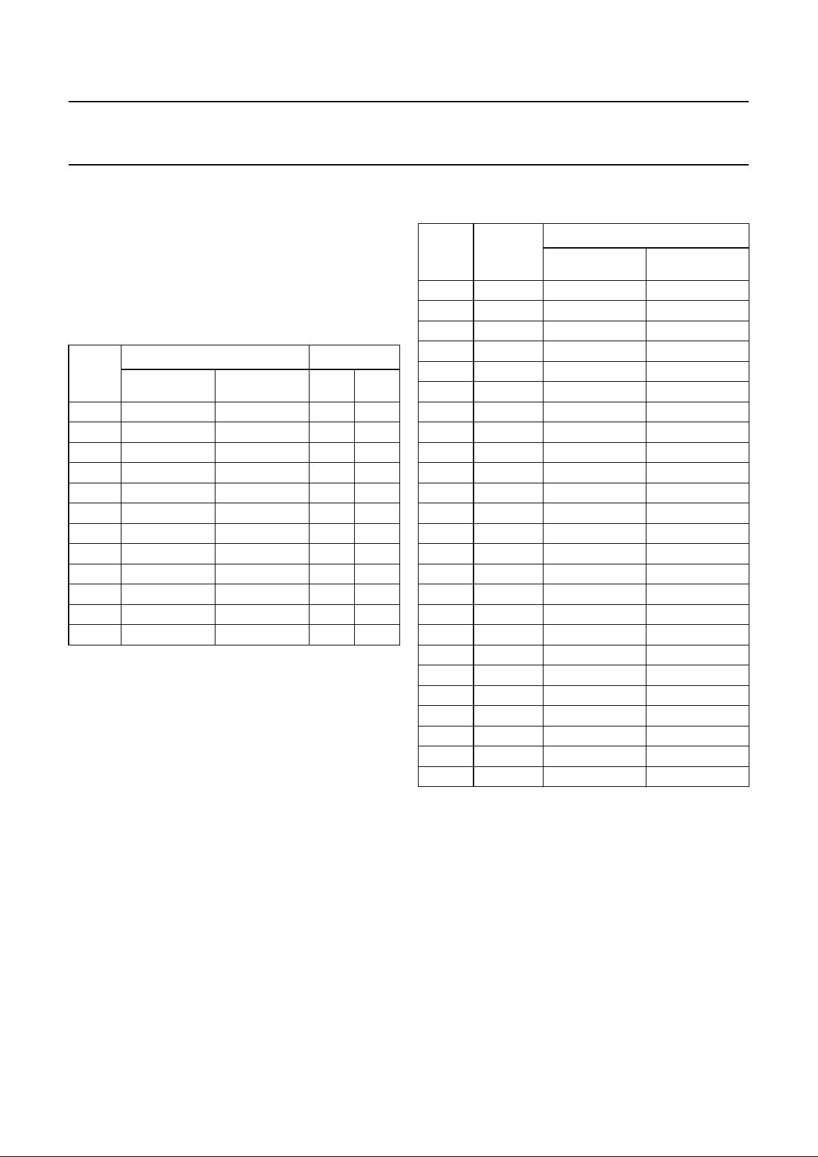
6.4 DTMF frequencies
Assuming an oscillator frequency f
xtal
= 3.58 MHz, the
DTMF standard frequencies can be implemented as
shown in Table 7.
The relationships between telephone keyboard symbols,
DTMFfrequencypairsandthefrequencyregistercontents
are given in Table 8.
Table 7 DTMF standard frequencies and their
implementation; value = LGF, HGF contents
Table 8 Dialling symbols, corresponding DTMF
frequency pairs and frequency register contents
f
f
xtal
23 x 2+()[]
-----------------------------
=
VALUE
(HEX)
FREQUENCY (Hz) DEVIATION
STANDARD GENERATED (%) (Hz)
DD 697 697.90 0.13 0.90
C8 770 770.46 0.06 0.46
B5 852 850.45 −0.18 −1.55
A3 941 943.23 0.24 2.23
7F 1209 1206.45 −0.21 −2.55
72 1336 1341.66 0.42 5.66
67 1477 1482.21 0.35 5.21
5D 1633 1638.24 0.32 5.24
TELEPHONE
KEYBOARD
SYMBOLS
DTMF FREQ.
PAIRS
(Hz)
LGF
VALUE
(HEX)
HGF
VALUE
(HEX)
0 (941, 1336) A3 72
1 (697, 1209) DD 7F
2 (697, 1336) DD 72
3 (697, 1477) DD 67
4 (770, 1209) C8 7F
5 (770, 1336) C8 72
6 (770, 1477) C8 67
7 (852, 1209) B5 7F
8 (852, 1336) B5 72
9 (852, 1477) B5 67
A (697, 1633) DD 5D
B (770, 1633) C8 5D
C (852, 1633) B5 5D
D (941, 1633) A3 5D
• (941, 1209) A3 7F
# (941, 1477) A3 67
1999 Oct 28 11
Philips Semiconductors Product specification
8-bit microcontrollers with DTMF generator
and 128 bytes EEPROM
PCA3351C; 52C; 53C;
PCD3351A; 52A; 53A
6.5 Modem frequencies
Again assuming an oscillator frequency f
xtal
= 3.58 MHz,
the standard modem frequencies can be implemented as
in Table 9. It is suggested to define the frequency by the
HGF register while the LGF register contains 00H,
disabling Low Group Frequency generation.
Table 9 Standard modem frequencies and their
implementation
Notes
1. Standard is V.21.
2. Standard is Bell 103.
3. Standard is Bell 202.
4. Standard is V.23.
6.6 Musical scale frequencies
Finally, two octaves of musical scale in steps of semitones
can be realized, again assuming an oscillator frequency
f
xtal
= 3.58 MHz (Table 10). It is suggested to define the
frequency by the HGF register while the LGF contains
00H, disabling Low Group Frequency generation
Table 10 Musical scale frequencies and their
implementation
Note
1. Standard scale based on A4 @ 440 Hz.
HGF
VALUE
(HEX)
FREQUENCY (Hz) DEVIATION
MODEM GENERATED (%) (Hz)
9D 980
(1)
978.82 −0.12 −1.18
82 1180
(1)
1179.03 −0.08 −0.97
8F 1070
(2)
1073.33 0.31 3.33
79 1270
(2)
1265.30 −0.37 −4.70
80 1200
(3)
1197.17 −0.24 −2.83
45 2200
(3)
2192.01 −0.36 −7.99
76 1300
(4)
1296.94 −0.24 −3.06
48 2100
(4)
2103.14 0.15 3.14
5C 1650
(1)
1655.66 0.34 5.66
52 1850
(1)
1852.77 0.15 2.77
4B 2025
(2)
2021.20 −0.19 −3.80
44 2225
(2)
2223.32 −0.08 −1.68
NOTE
HGF
VALUE
(HEX)
FREQUENCY (Hz)
STANDARD
(1)
GENERATED
D#5 F8 622.3 622.5
E5 EA 659.3 659.5
F5 DD 698.5 697.9
F#5 D0 740.0 741.1
G5 C5 784.0 782.1
G#5 B9 830.6 832.3
A5 AF 880.0 879.3
A#5 A5 923.3 931.9
B5 9C 987.8 985.0
C6 93 1046.5 1044.5
C#6 8A 1108.7 1111.7
D6 82 1174.7 1179.0
D#6 7B 1244.5 1245.1
E6 74 1318.5 1318.9
F6 6D 1396.9 1402.1
F#6 67 1480.0 1482.2
G6 61 1568.0 1572.0
G#6 5C 1661.2 1655.7
A6 56 1760.0 1768.5
A#6 51 1864.7 1875.1
B6 4D 1975.5 1970.0
C7 48 2093.0 2103.3
C#7 44 2217.5 2223.3
D7 40 2349.3 2358.1
D#7 3D 2489.0 2470.4
 Loading...