

Philips PBYR4020WT, PBYR4025WT Datasheet
Philips Semiconductors Product specification
Rectifier diodes PBYR4025WT series
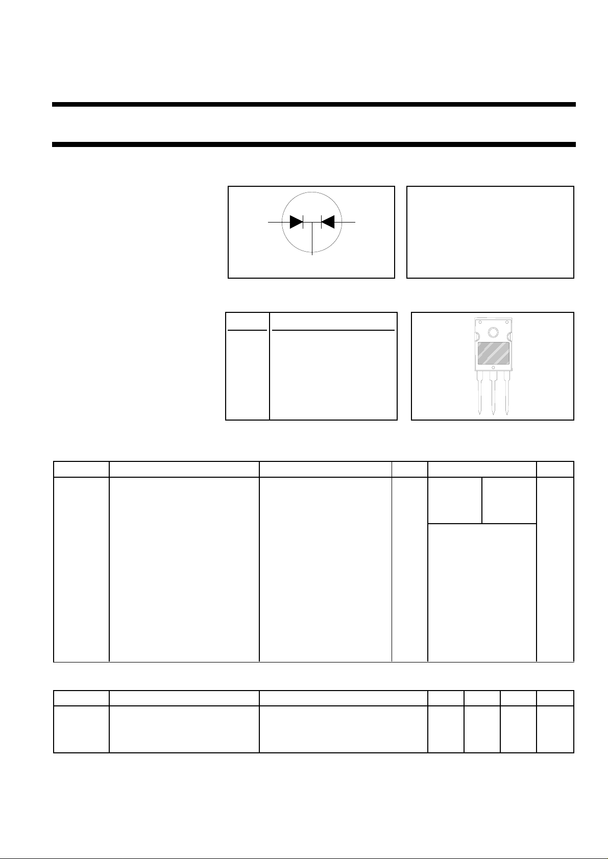
schottky barrier
FEATURES SYMBOL QUICK REFERENCE DATA
• Low forward volt drop
• Fast switching V
• Reverse surge capability
• High thermal cycling performance I
a1
13
a2
• Low thermal resistance
k
2
GENERAL DESCRIPTION PINNING SOT429 (TO247)
Dual, common cathode schottky PIN DESCRIPTION
rectifier diodes in a plastic
envelope. Intended for use as 1 anode 1 (a)
output rectifiersin low voltage, high
frequency switched mode power 2 cathode (k)
supplies.
The PBYR4025WT series is
suppliedintheconventionalleaded tab cathode
SOT429 (TO247) package.
3 anode 2 (a)
= 20 V / 25 V
R
= 40 A
O(AV)
VF ≤ 0.46 V
2
3
1
LIMITING VALUES
Limiting values in accordance with the Absolute Maximum System (IEC 134).
SYMBOL PARAMETER CONDITIONS MIN. MAX. UNIT
-20 -25
V
V
V
I
O(AV)
I
FRM
I
FSM
RRM
RWM
R
Repetitive peak reverse voltage - 20 25 V
Crest working reverse voltage - 20 25 V
Continuous reverse voltage Tmb ≤ 109 ˚C - 20 25 V
Average output current (both square wave; δ = 0.5; - 40 A
diodes conducting) Tmb ≤ 128 ˚C
Repetitive peak forward current t = 25 µs; δ = 0.5; - 40 A
per diode Tmb ≤ 128 ˚C
Non-repetitive peak forward t = 10 ms - 180 A
current, per diode t = 8.3 ms - 200 A
sinusoidal Tj = 125 ˚C prior
to surge; with reapplied
V
I
RRM
T
T
stg
j
Repetitive peak reverse current tp = 2 µs; δ = 0.001 - 2 A
per diode
Storage temperature -65 175 ˚C
Operating junction temperature - 150 ˚C
RRM(max)
THERMAL RESISTANCES
SYMBOL PARAMETER CONDITIONS MIN. TYP. MAX. UNIT
R
R
th j-mb
th j-a
Thermal resistance junction to per diode - - 1.5 K/W
mounting base both diodes - - 1.0 K/W
Thermal resistance junction to in free air - 45 - K/W
ambient
November 1998 1 Rev 1.100
Philips Semiconductors Product specification
Rectifier diodes PBYR4025WT series
schottky barrier
STATIC CHARACTERISTICS
Tj = 25 ˚C unless otherwise stated
SYMBOL PARAMETER CONDITIONS MIN. TYP. MAX. UNIT
V
F
I
R
C
d
Forward voltage (per diode) IF = 20 A; Tj = 125˚C - 0.40 0.46 V
IF = 40 A; Tj = 125˚C - 0.50 0.54 V
IF = 40 A - 0.60 0.64 V
Reverse current (per diode) VR = V
Junction capacitance (per f = 1MHz; VR = 5V; Tj = 25 ˚C to - 900 - pF
VR = V
RRM
; Tj = 100 ˚C - 30 80 mA
RRM
- 2.0 10 mA
diode) 125 ˚C
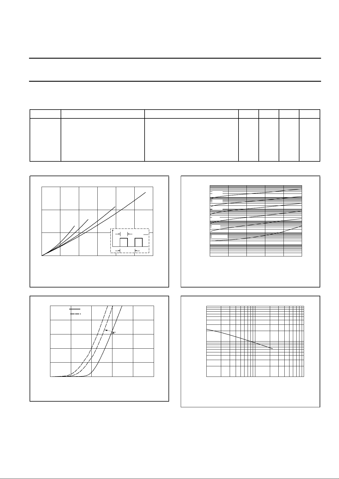
PF / W
15
Vo = 0.38 V
Rs = 0.004 Ohms
10
5
0
0 5 10 15 20 25 30
PBYR4025WT
0.2
0.1
IF(AV) / A
I
Tmb(max) / C
0.5
t
p
T
D = 1.0
D =
Fig.1. Maximum forward dissipation PF = f(I
diode; square current waveform where
I
50
40
30
20
IF / A
Tj = 25 C
Tj = 125 C
F(AV)
=I
x √D.
F(RMS)
PBYR1625
typ
max
p
t
T
t
F(AV)
127.5
135
142.5
150
) per
IR / A
1A
150 C
100mA
125 C
10mA
100 C
75 C
1mA
50 C
100uA
Tj = 25 C
10uA
1uA
0 5 10 15 20 25
PBYR1625
VR / V
Fig.3. Typical reverse leakage current per diode;
10000
1000
IR = f(VR); parameter T
Cd / pF
PBYR1625
j
10
0
0 0.2 0.4 0.6 0.8 1
VF / V
Fig.2. Typical and maximum forward characteristic
IF = f(VF); parameter T
j
100
1 10 100
VR / V
Fig.4. Typical junction capacitance per diode;
Cd = f(VR); f = 1 MHz; Tj = 25˚C to 125 ˚C.
November 1998 2 Rev 1.100
 Loading...