

Philips PBYR3045PT Datasheet
Philips Semiconductors Product specification
Rectifier diodes PBYR3045PT series
schottky barrier
GENERAL DESCRIPTION QUICK REFERENCE DATA
Dual, low leakage, platinum barrier, SYMBOL PARAMETER MAX. MAX. MAX. UNIT
schottky rectifier diodes in a plastic
envelope featuring low forward PBYR30- 35PT 40PT 45PT
voltage drop and absence of stored V
RRM
charge.Thesedevices can withstand voltage
reverse voltage transients and have V
guaranteed reversesurge capability. I
F
O(AV)
The devices are intended for use in diodes conducting)
switched mode power supplies and
high frequency circuits in general
where low conduction and zero
switching losses are important.
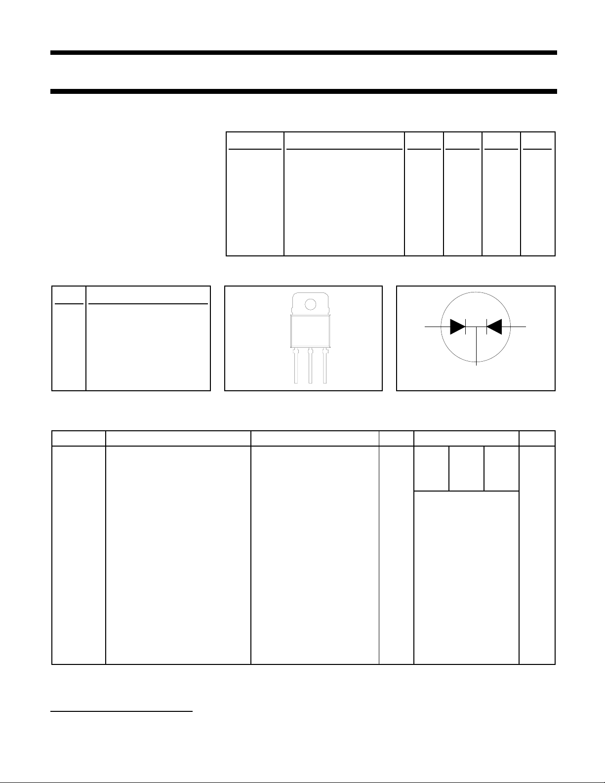
PINNING - SOT93 PIN CONFIGURATION SYMBOL
Repetitive peak reverse 35 40 45 V
Forward voltage 0.60 0.60 0.60 V
Output current (both 30 30 30 A
PIN DESCRIPTION
tab
1 Anode 1 (a)
2 Cathode (k)
a1
1
a2
3
3 Anode 2 (a)
k
tab Cathode (k)
123
2
LIMITING VALUES
Limiting values in accordance with the Absolute Maximum System (IEC 134).
SYMBOL PARAMETER CONDITIONS MIN. MAX. UNIT
V
RRM
V
RWM
V
R
I
O(AV)
I
O(RMS)
I
FRM
I
FSM
Repetitive peak reverse voltage - 35 40 45 V
Crest working reverse voltage - 35 40 45 V
Continuous reverse voltage Tmb ≤ 136 ˚C - 35 40 45 V
Output current (both diodes square wave; δ = 0.5; - 30 A
conducting)
RMS forward current - 43 A
Repetitive peak forward current t = 25 µs; δ = 0.5; - 30 A
per diode Tmb ≤ 130 ˚C
Non-repetitive peak forward t = 10 ms - 180 A
current per diode t = 8.3 ms - 200 A
I2tI
I
RRM
2
t for fusing t = 10 ms - 162 A2s
Repetitive peak reverse current tp = 2 µs; δ = 0.001 - 2 A
per diode.
I
RSM
T
T
stg
j
Non-repetitive peak reverse tp = 100 µs-2A
current per diode.
Storage temperature -65 175 ˚C
Operating junction temperature - 150 ˚C
1
Tmb ≤ 130 ˚C
sinusoidal Tj = 125 ˚C prior
to surge; with reapplied
V
RWM(max)
-35 -40 -45
1 For output currents in excess of 20 A connection should be made to the exposed metal mounting base.
August 1996 1 Rev 1.100

Philips Semiconductors Product specification
Rectifier diodes PBYR3045PT series
schottky barrier
THERMAL RESISTANCES
SYMBOL PARAMETER CONDITIONS MIN. TYP. MAX. UNIT
R
th j-mb
R
th j-a
STATIC CHARACTERISTICS
Tj = 25 ˚C unless otherwise stated
SYMBOL PARAMETER CONDITIONS MIN. TYP. MAX. UNIT
V
F
I
R
C
d
Thermal resistance junction to per diode - - 1.4 K/W
mounting base both diodes - - 1.0 K/W
Thermal resistance junction to in free air. - 45 - K/W
ambient
Forward voltage (per diode) IF = 20 A; Tj = 125˚C - 0.55 0.60 V
IF = 30 A; Tj = 125˚C - 0.67 0.72 V
IF = 30 A - 0.71 0.76
Reverse current (per diode) VR = V
VR = V
RWM
; Tj = 125 ˚C - 12 40 mA
RWM
- 100 200 µA
Junction capacitance (per f = 1MHz; VR = 5V; Tj = 25 ˚C to - 800 - pF
diode) 125 ˚C
August 1996 2 Rev 1.100
 Loading...