Philips PBYR3035PTF, PBYR3040PTF, PBYR3045PTF Datasheet

0 (0)
Philips PBYR3035PTF, PBYR3040PTF, PBYR3045PTF Datasheet

Philips Semiconductors Product specification

Rectifier diodes


PBYR3045PTF series


schottky barrier


GENERAL DESCRIPTION

QUICK REFERENCE DATA


Dual, low leakage, platinum barrier,


SYMBOL


PARAMETER


MAX.


MAX.


MAX.


UNIT


schottky barrier rectifier diodes in a


PBYR30-

35PTF

40PTF

45PTF


full pack, plastic envelope featuring


low forward voltage drop and


VRRM


Repetitive peak reverse


35


40


45


V


absence of stored charge. These


voltage


devices

can withstand

reverse


VF


Forward voltage


0.65


0.65


0.65


V


voltage

transients and

have


IO(AV)


Output current (both


20


20


20


A


guaranteed reverse surge capability.


diodes conducting)


The devices are intended for use in


switched mode power supplies and


high frequency circuits in general


where low conduction and zero


switching losses are important.


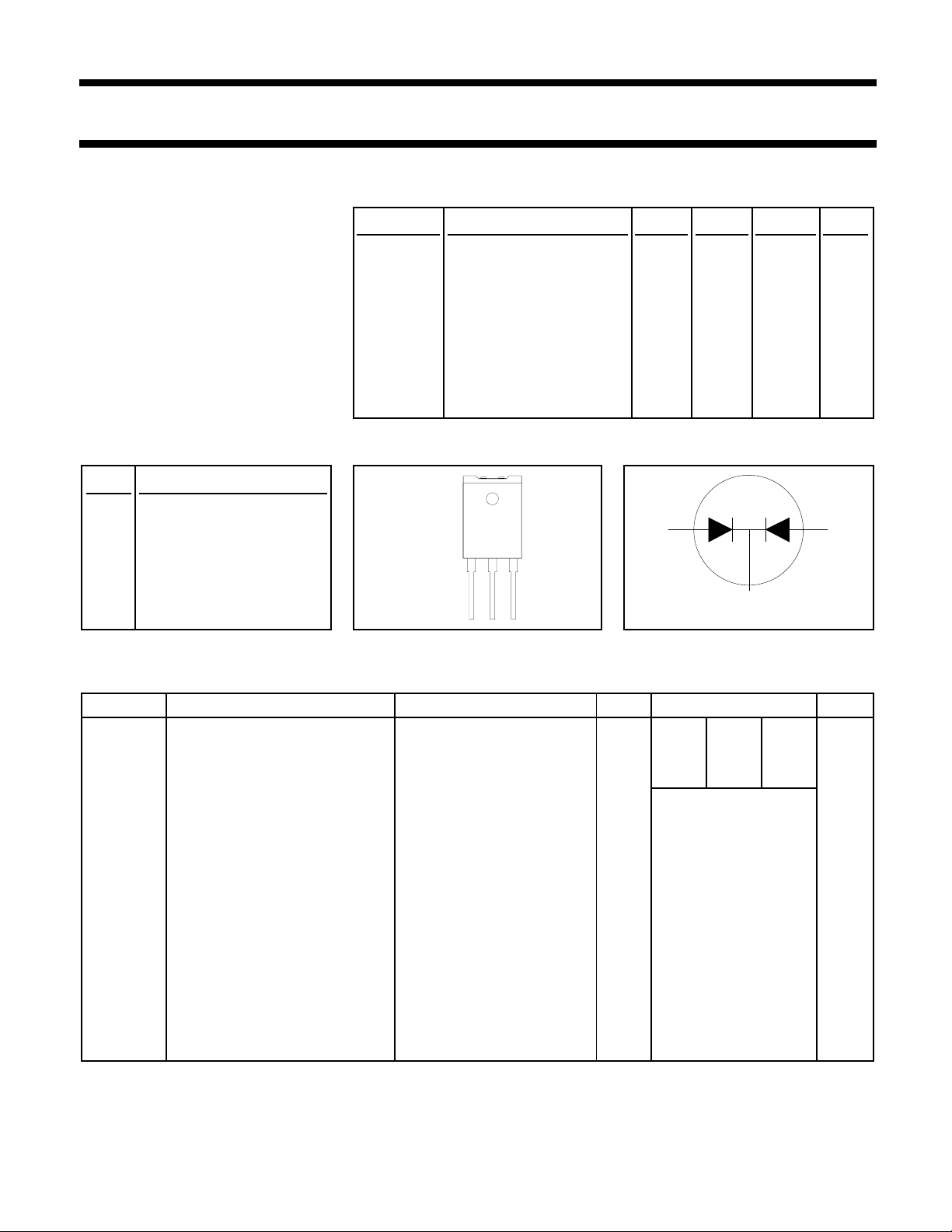
PINNING - SOT199


PIN CONFIGURATION


SYMBOL


PIN


DESCRIPTION


case


1


anode 1 (a)


a1


a2


2


cathode (k)


1


3


3


anode 2 (a)


1

2

3


k


2


LIMITING VALUES


Limiting values in accordance with the Absolute Maximum System (IEC 134).


SYMBOL

PARAMETER


CONDITIONS


MIN.


MAX.


UNIT


-35


-40


-45


VRRM


Repetitive peak reverse voltage


-


35


40


45


V


VRWM


Crest working reverse voltage

Ths 113 ˚C


-


35


40


45


V


VR


Continuous reverse voltage


-


35


40


45


V


IO(AV)


Output current (both diodes

square wave; δ = 0.5;

-


20


A


conducting)


Ths

109 ˚C


IO(RMS)


RMS forward current


t = 25 μs; δ = 0.5;

-


20


A


IFRM


Repetitive peak forward current

-


30


A


per diode


Ths

109 ˚C


IFSM


Non-repetitive peak forward

t = 10 ms


-


135


A


current per diode.


t = 8.3 ms


-


150


A


sinusoidal; Tj = 125 ˚C prior


to surge; with reapplied


I2t


I2t for fusing


VRWM(max)


-


91


A2s


t = 10 ms


IRRM


Repetitive peak reverse current

tp = 2

μs;

δ = 0.001

-


2


A


per diode.


tp = 100 μs


IRSM


Non-repetitive peak reverse


-


2


A


current per diode.


Tstg


Storage temperature


-65


175


˚C


Tj


Operating junction temperature


-


150


˚C


August 1996

1

Rev 1.100

Philips Semiconductors Product specification

Rectifier diodes


PBYR3045PTF series


schottky barrier


ISOLATION LIMITING VALUE & CHARACTERISTIC


Ths = 25 ˚C unless otherwise specified


SYMBOL

PARAMETER


CONDITIONS


MIN.


TYP.

MAX.

UNIT


Visol

Repetitive peak voltage from all


R.H. 65 % ; clean and dustfree


-


2500

V


three terminals to external


heatsink


Cisol

Capacitance from T2 to external


f = 1 MHz


-


22

-

pF


heatsink


THERMAL RESISTANCES


SYMBOL

PARAMETER

CONDITIONS

MIN.

TYP.

MAX.

UNIT


Rth j-hs

Thermal resistance junction to

per diode

-


-

4.0

K/W


heatsink

both diodes

-


-

3.5

K/W


(with heatsink compound)


Rth j-a

Thermal resistance junction to

in free air.

-


35

-

K/W


ambient


STATIC CHARACTERISTICS


Tj = 25 ˚C unless otherwise stated


SYMBOL

PARAMETER

CONDITIONS

MIN.

TYP.

MAX.

UNIT


VF

Forward voltage (per diode)

IF = 30 A; Tj = 125˚C

-


0.70

0.75

V


IF = 20 A; Tj = 125˚C

-


0.58

0.65

V


IF = 30 A

-


0.75

0.80

V


IR

Reverse current (per diode)

VR = VRWM

-


100

200

μA


Cd


VR = VRWM; Tj = 125 ˚C

-


12

40

mA


Junction capacitance (per

f = 1MHz; VR = 5V; Tj = 25 ˚C to

-


800

-

pF


diode)

125 ˚C


August 1996

2

Rev 1.100

Loading...
+ 3 hidden pages