

Philips p90cl301bfh DATASHEETS

INTEGRATED CIRCUITS
DATA SH EET
P90CL301BFH (C100)
Low voltage 16-bit microcontroller
Preliminary specification
File under Integrated Circuits, IC17
1996 Dec 11

Philips Semiconductors Preliminary specification
Low voltage 16-bit microcontroller P90CL301BFH (C100)
CONTENTS
1 FEATURES
2 DESCRIPTION
2.1 Compatibility between P90CL301AFH and
P90CL301BFH
3 ORDERING INFORMATION
4 BLOCK DIAGRAM
5 PINNING INFORMATION
5.1 Pinning
5.2 Pin description
6 SYSTEM CONTROL
6.1 Memory organization
6.2 Programmable chip-select
6.3 Dynamic bus port sizing
6.4 System Control Register (SYSCON)
6.5 Reset operation
6.6 Clock generation
6.7 Interrupt controller
6.8 Power reduction modes
7 CPU FUNCTIONAL DESCRIPTION
7.1 General
7.2 Programming model and data organization
7.3 Processing states and exception processing
7.4 Tracing
7.5 Stack format
7.6 CPU interrupt processing
7.7 Bus arbitration
8 PORTS
8.1 Port P Control Register (PCON)
8.2 Port SP
8.3 Ports schematics
9 8051 PERIPHERAL BUS
10 ON-CHIP PERIPHERAL FUNCTIONS
10.1 Peripheral interrupt control
11 TIMERS
11.1 Timer array
11.2 Timebase
11.3 Channel function
11.4 Pin parallel functions for the timer
11.5 Timer Control Registers
11.6 Timer Status Register
11.7 Watchdog Timer
12 SERIAL INTERFACES
12.1 UART interface
12.2 Baud rate generator
12.3 UART queue
12.4 I2C-bus interface
12.5 Serial Control Register (SCON)
13 PULSE WIDTH MODULATION OUTPUTS
(PWM)
13.1 Prescaler PWM Register (PWMP)
13.2 PWM Data Registers (PWM0 and PWM1)
14 ANALOG-TO-DIGITAL CONVERTER (ADC)
14.1 ADC Control Register (ADCON)
15 ON-BOARD TEST CONCEPT
15.1 ONCE mode
15.2 Test ROM
16 ON-CHIP RAM
17 REGISTER MAPPING
18 LIMITING VALUES
19 DC CHARACTERISTICS
20 ADC CHARACTERISTICS
21 AC CHARACTERISTICS
22 8051 BUS TIMING
23 TIMING DIAGRAMS
24 CLOCK TIMING
25 PIN STATES IN VARIOUS MODES
26 INSTRUCTION SET AND ADDRESSING
MODES
26.1 Addressing modes
27 INSTRUCTION TIMING
28 PACKAGE OUTLINE
29 SOLDERING
29.1 Introduction
29.2 Reflow soldering
29.3 Wave soldering
29.4 Repairing soldered joints
30 DEFINITIONS
31 LIFE SUPPORT APPLICATIONS
32 PURCHASE OF PHILIPS I2C COMPONENTS
1996 Dec 11 2

Philips Semiconductors Preliminary specification
Low voltage 16-bit microcontroller P90CL301BFH (C100)
1 FEATURES
• Fully 68000 software compatible
• Static design with 32-bit internal structure
• Power saving modes: Power-down, Standby and Idle
mode
• External clock input: 27 MHz at 2.7 V
• Single supply voltage of 2.7 to 3.6 V; down to 1.8 V for
RAM retention
• 68000 compatible bus interface
• Intel 8051 compatible bus interface
• 16 Mbytes program/data address range
• 8 programmable chip-selects
• Dynamic bus sizing, 16 or 8-bit memory bus port size
• 56 powerful instruction types:
– 5 basic data types, and
– 14 addressing modes
• 7 programmable interrupt inputs:
– a Non-Maskable Interrupt input (NMIN)
– 14 auto-vectored interrupts and 7 interrupt priority
levels
• 24 port pins (multiplexed with other functions)
• 2 UART serial interfaces; an independent baud rate
generator with two programmable outputs (UART0 and
UART1)
• UART queue with maximum 256 bytes
2
C-bus serial interface 100 kbaud
• I
• 2 timer arrays including:
– two 16-bit reference counters and 8-bit
programmable prescalers
– six 16-bit match/capture registers with equality
comparators
• Watchdog Timer with 21-bit resolution
• Two 8-bit Pulse Width Modulation (PWM) outputs with
8-bit prescaler
• Four 8-bit Analog-to-Digital Converter (ADC) inputs with
Power-down mode
• 512 bytes RAM on-chip
• On-Circuit Emulation (ONCE) mode and internal
Test-ROM (256 bytes) for on-board testing
• 80-pin LQFP package
• Temperature range −40 to +85 °C
• 0.5 micron CMOS low voltage technology.
2 DESCRIPTION
The P90CL301BFH is a highly integrated low-voltage
16/32-bit microcontroller especially suitable for digital
mobile systems such as GSM, DCS1900, IS54/95 and
other applications requiring low voltage, low power
consumption and high computing power. It is fully software
compatible with the 68000.
The P90CL301BFH optimizes system cost by providing
both standard as well as advanced peripheral functions
on-chip. The P90CL301BFH has a full static design and
special Idle, Standby and Power-down modes which allow
further reduction of the total system power consumption.
An 80-pin LQFP package dramatically reduces system
size requirements.
2.1 Compatibility between P90CL301AFH and P90CL301BFH
For functional compatibility between P90CL301AFH
(SAC1 process) and P90CL301BFH (C100 process), the
following points should be considered when using the
P90CL301BFH:
• Wake-up; to wake-up the processor from Power-down
mode via the activation of an external SPn pin, it is
necessary to enable the interrupt mode first by setting
the corresponding bit in the SPCON register.
• SYSCON register; for the P90CL301AFH bits 11 to 15
in the SYSCON register should not be set in order to
keep additional functionality in the P90CL301BFH
inactive.
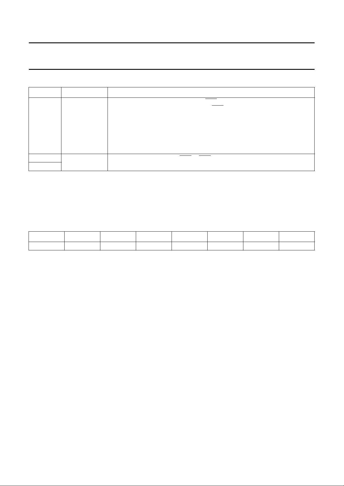
3 ORDERING INFORMATION
PACKAGE
TYPE NUMBER
NAME DESCRIPTION VERSION
P90CL301BFH LQFP80 plastic low profile quad flat package; 80 leads;
body 12 × 12 × 1.4 mm
1996 Dec 11 3
TEMPERATURE
RANGE (°C)
SOT315-1 −40 to +85
Philips Semiconductors Preliminary specification
Low voltage 16-bit microcontroller P90CL301BFH (C100)
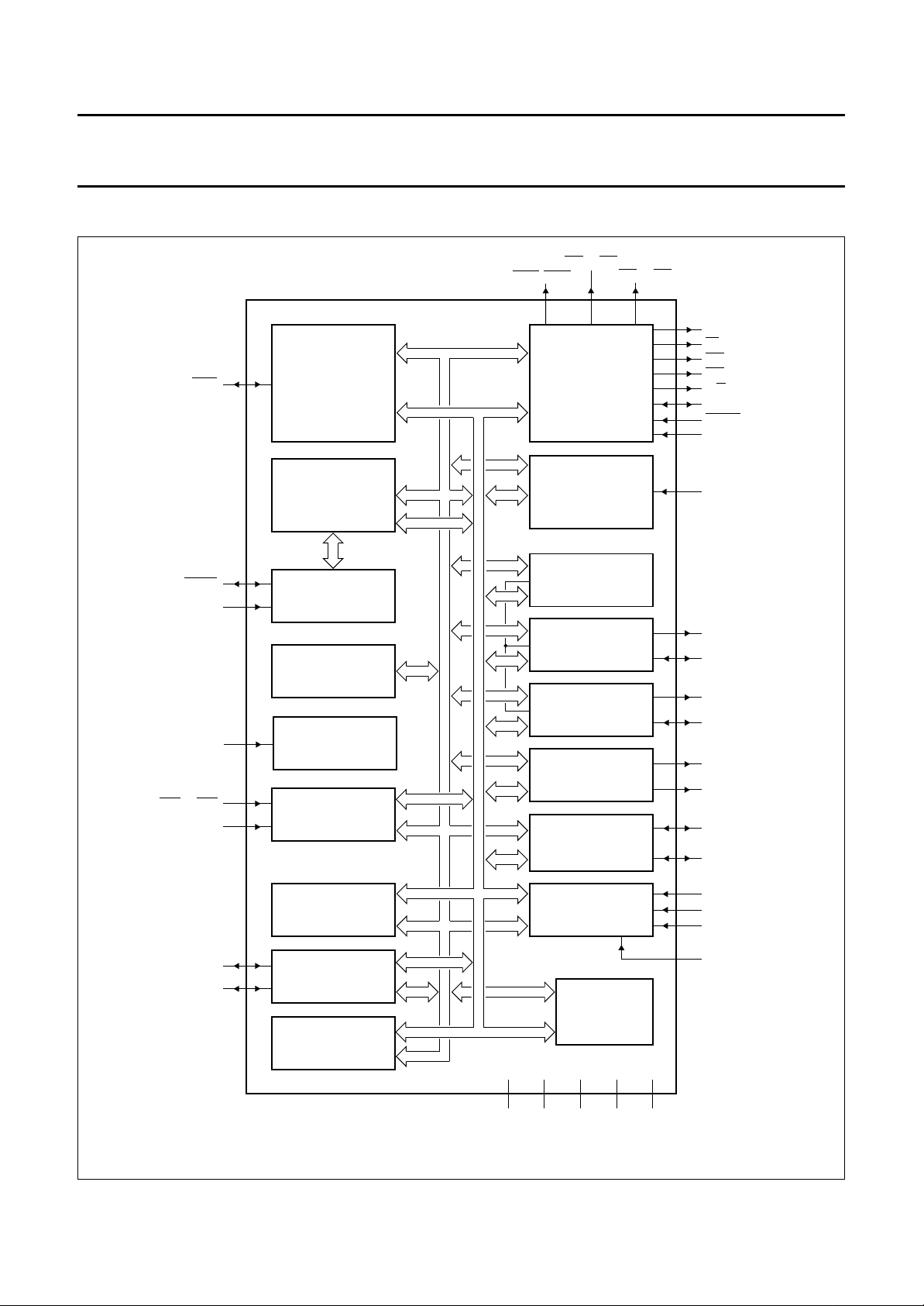
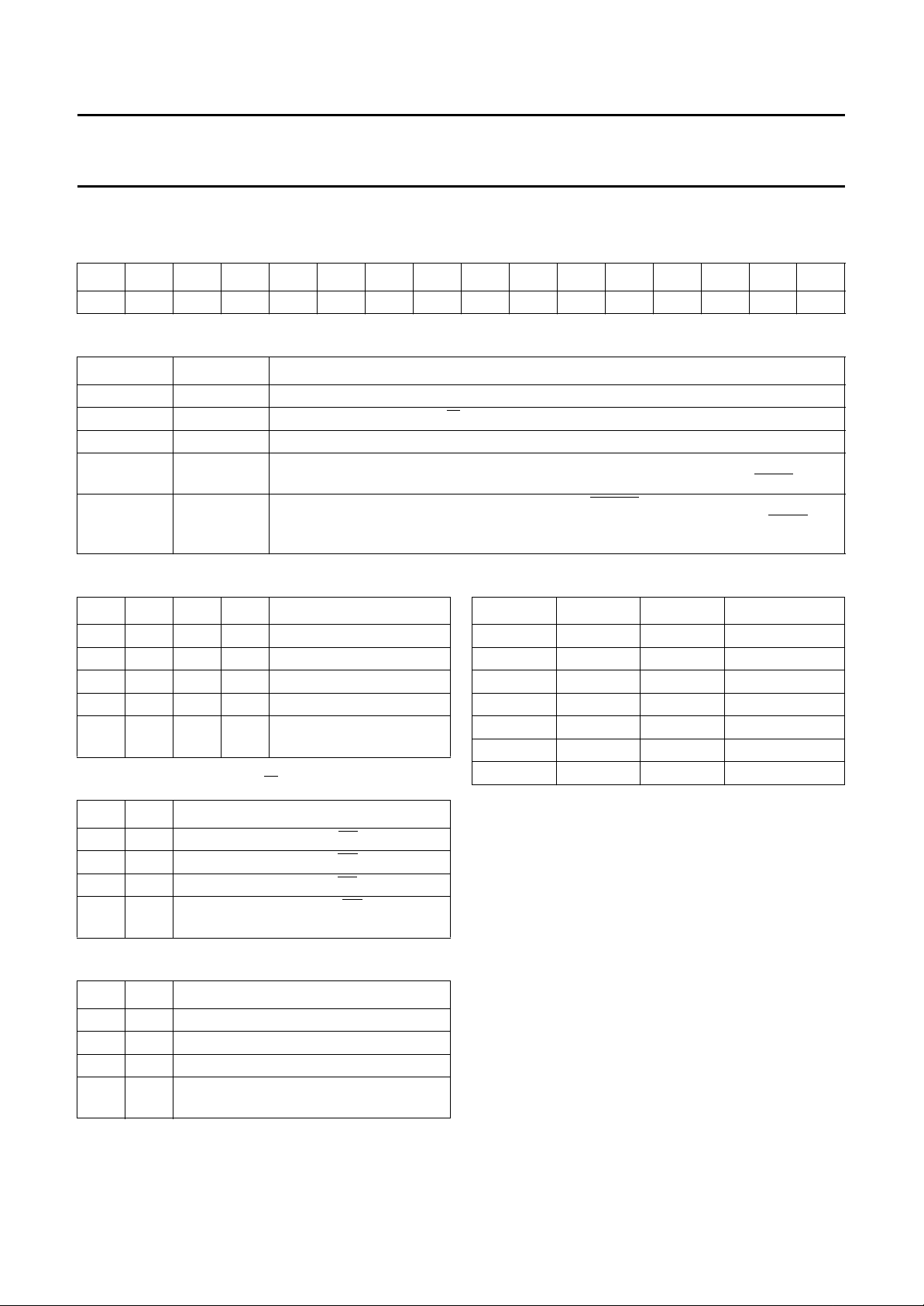
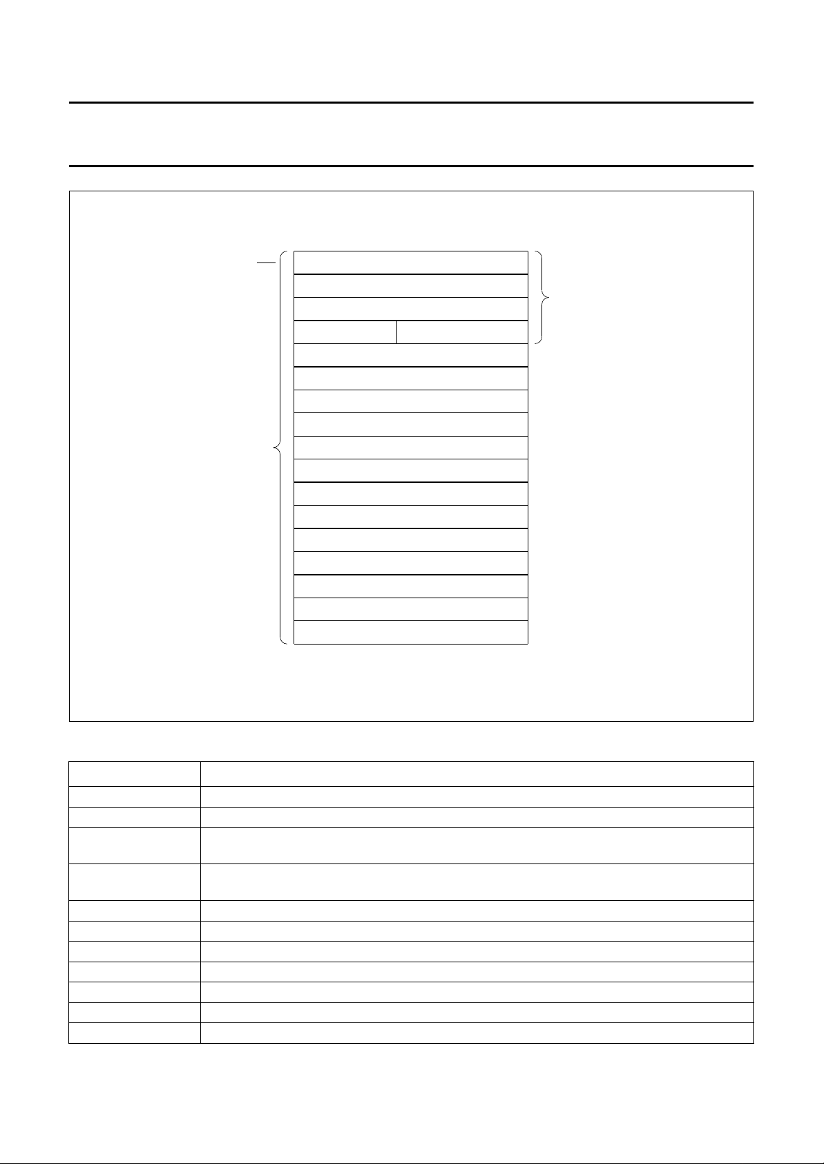
4 BLOCK DIAGRAM
andbook, full pagewidth
INT0 to INT6
HALT
RESET
RESETIN
XTAL1
NMIN
CPU 68000
WATCHDOG
TIMER
RESET
SYSTEM CTRL
CLOCK
INTERRUPTS
D15 to D0
A31 to A0
CSBT/ONCE
2 × 16-BIT TIMERS
6 CHANNELS
GENERATOR
CS0 to CS2
BUS
INTERFACE
BAUD RATE
UART0
UART1
PWM
2
I
C-BUS
INTERFACE
CS3 to CS6
A23 to A1
AS
LDS
UDS
R/W
D15 to D0
DTACK
BSIZE
CP0 to CP5
TX0
RX0
TX1
RX1
PWM0
PWM1
SCL
SDA
RAM
512 BYTES
SP0 to SP7
P0 to P15
PORT
TEST ROM
data bus
D15 to D0
Fig.1 P90CL301BFH block diagram.
1996 Dec 11 4
address bus
A31 to A0
V
V
DD1
DD2
8-BIT ADC
UART QUEUE
V
V
SS1
DD3
V
SS2
V
DDA
V
SSA
ADC0 to ADC3
V
ref(A)
MGD780
Philips Semiconductors Preliminary specification
Low voltage 16-bit microcontroller P90CL301BFH (C100)
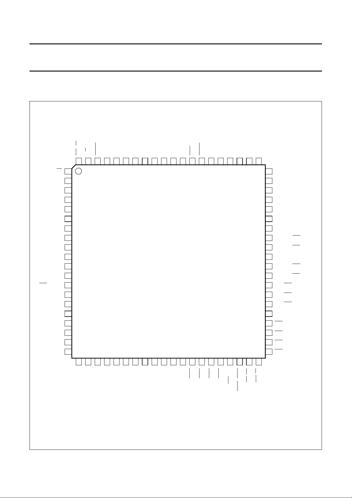
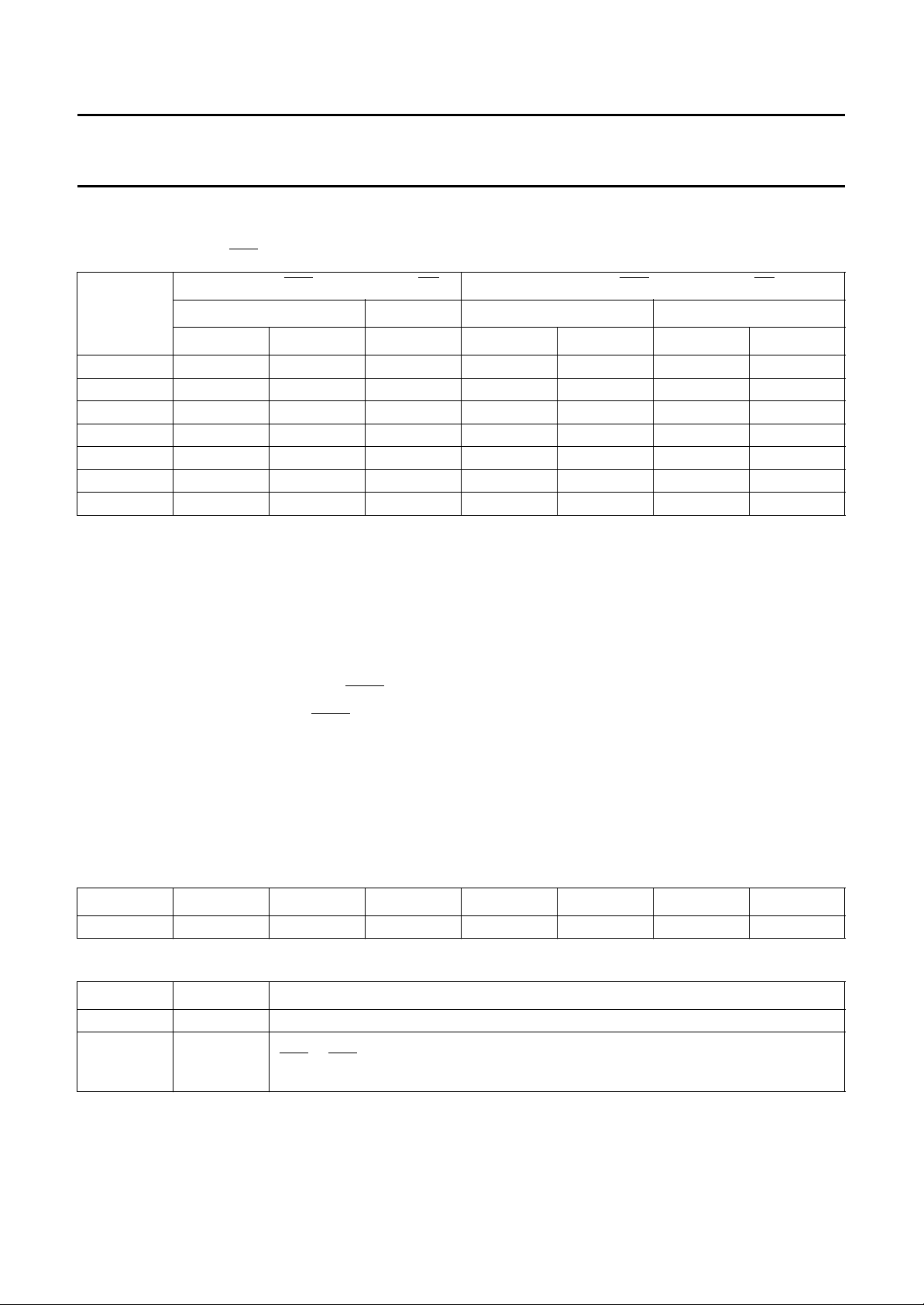
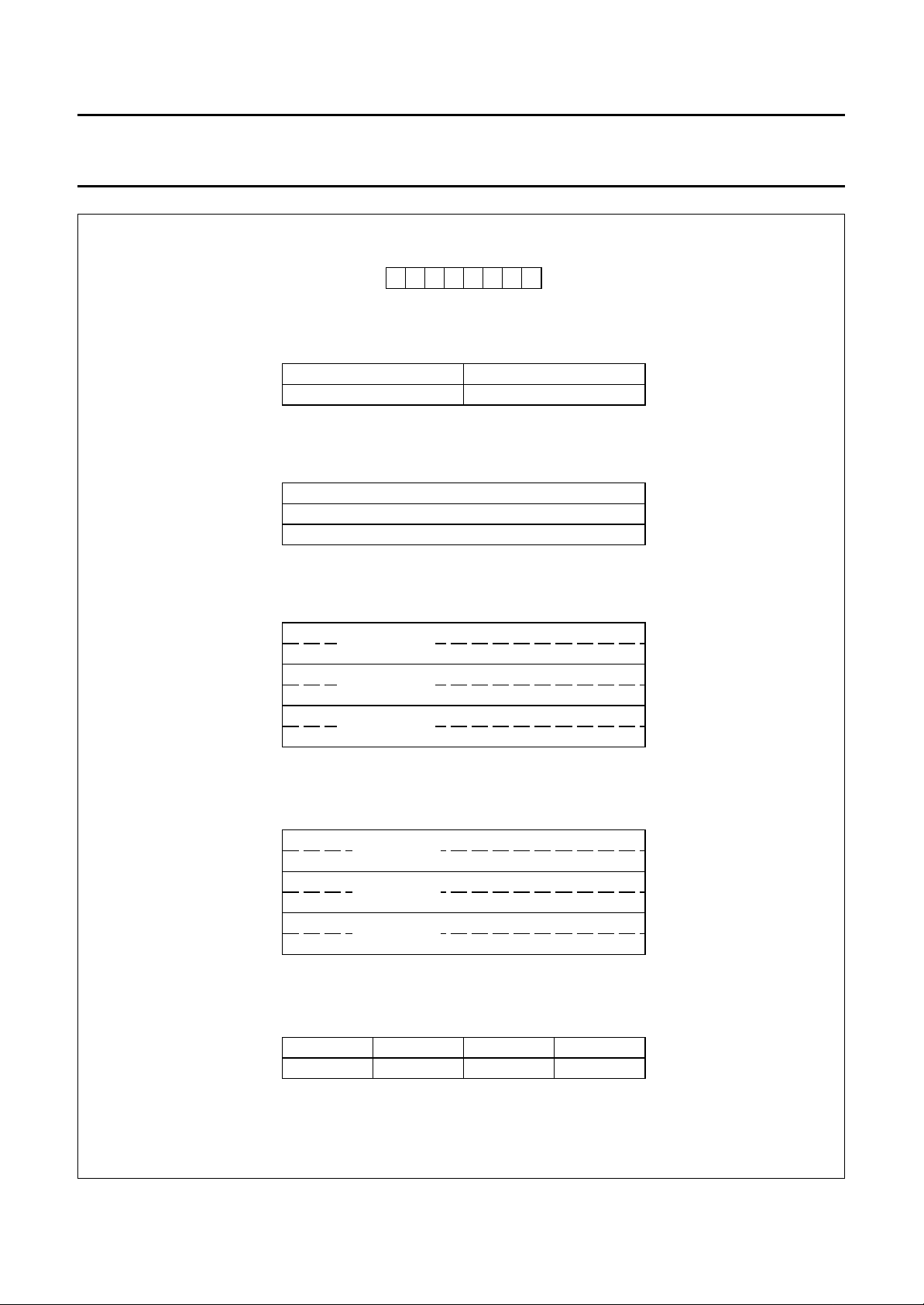
5 PINNING INFORMATION
5.1 Pinning
dbook, full pagewidth
D7
D6
D5
D4
D3
D2
D1
D0
V
DD3
XTAL1
V
SS1
UDS/A0/AD0
A1/AD1
A2/AD2
A3/AD3
A4/AD4
A5/AD5
A6/AD6
A7/AD7
LDS [DS]
R/W / TROM
DTACK
D8/P0
D9/P1
D10/P2
D11/P3
D12/P4
D13/P5
D14/P6
80
79
78
77
76
75
74
73
72
71
1AS
2
3
4
5
6
7
8
9
10
11
12
13
14
15
16
17
18
19
20
21
22
23
24
25
26
A8
A9
A10
A11
A12
A13
27
A14
28
A15
P90CL301BFH
29
30
A16
A17
D15/P7
V
70
31
A18
DD1
69
32
DD2
V
HALT
RESET
68
67
33
34
A19/PCS0
A20/PCS1
SSA
RESETIN
V
66
65
35
36
A21/PCS2
A22/PCS3
P12/ADC0
P13/ADC1
64
63
37
38
CS6/A23
CSBT/ONCE
ref(A)
P14/ADC2
V
62
61
39
40
CS4/RD
CS5/WR
P15/ADC3
60
V
59
DDA
BSIZE
58
57
P11/SDA
56
P10/SCL
55
P9/PWM1 (CP1)
54
P8/PWM0 (CP0)
SP0/RX1/INT0
53
52
SP1/TX1/INT1 (CLK0)
51
V
SS2
50
SP2/RX0/INT2 (CP2)
49
SP3/TX0/INT3 (CP3)
48
SP4/INT4 (CP4)
47
SP5/INT5 (CP5)
46
SP6/INT6 (CLK1)
NMIN/SP7
45
44
CS0/FC0
43
CS1/FC1
CS2/FC2
42
CS3/ALE
41
MGD773
Fig.2 Pinning diagram of the P90CL301BFH (LQFP80).
1996 Dec 11 5
Philips Semiconductors Preliminary specification
Low voltage 16-bit microcontroller P90CL301BFH (C100)
5.2 Pin description
Table 1 Pin description for the P90CL301BFH
SYMBOL
AS 1 address strobe
D7 to D0 2 to 9 lower 8-bits of data bus
V
DD3
XTAL1 11 external clock input
V
SS1
UDS/A0/AD0 13 upper data strobe or LSB of address bus or LSB of 8051 address/data
A1/AD1 to A7/AD7 14 to 20 lower 7-bits of the 68000 address bus or lower 7-bits of the 8051 bus
A8 to A18 21 to 31 upper 11-bits of the 68000 address bus
V
DD2
A19/
PCS0 to A22/PCS3 33 to 36 upper 4-bits of the address bus or 8051 bus chip-select
CS6/A23 37 chip-select 6 or address bit 23
CSBT/ONCE 38 chip-select boot or ONCE mode forced input
CS5/WR 39 chip-select 5 or 8051 bus write strobe
CS4/RD 40 chip-select 4 or 8051 bus read strobe
CS3/ALE 41 chip-select 3 or 8051 bus address latch
CS2/FC2 to CS0/FC0 42 to 44 chip-select 2 to 0 or data bus function code 2 to 0
NMIN/SP7 45 Non-Maskable Interrupt or second port pin (bit 7)
INT6 (CLK1) 46 second port pin (bit 6) external interrupt input 6 (external clock of timer 1)
SP6/
INT5 (CP5) 47 second port pin (bit 5) or external interrupt input 5 (Timer 1 capture input 5)
SP5/
INT4 (CP4) 48 second port pin (bit 4) or external interrupt input 4 (Timer 1 capture input 4)
SP4/
SP3/TX0/
SP2/RX0/
V
SS2
SP1/TX1/
SP0/RX1/
P8/PWM0 (CP0) 54 port pin (bit 8) or PWM0 output (Timer 0 capture input 0)
P9/PWM1 (CP1) 55 port pin (bit 9) or PWM1 output (Timer 0 capture input 1)
P10/SCL 56 port pin (bit 10) or I
P11/SDA 57 port pin (bit 11) or I
BSIZE 58 data bus size; 8 or 16-bit wide
V
DDA
P15/ADC3 60 port pin (bit 15) or ADC input 3
V
ref(A)
P14/ADC2 to P12/ADC0 62 to 64 port pin (bit 14 to bit 12) or ADC inputs 2 to 0
V
SSA
RESETIN 66 external Power-on-reset input
(1)
PIN DESCRIPTION
10 supply voltage; third pin
12 ground; first pin
32 supply voltage; second pin
INT3 (CP3) 49 second port pin (bit 3) or Transmit data for UART0 or external interrupt input 3
(Timer 1 capture input 3)
INT2 (CP2) 50 second port pin (bit 2) or Receive data for UART0 or external interrupt input 2
(Timer 0 capture input 2)
51 ground; second pin
INT1 (CLK0) 52 second port pin (bit 1) or transmit data for UART1 or external interrupt input 1
(external clock of Timer 0)
INT0 53 second port pin (bit 0) or receive data for UART1 or external interrupt input 0
2
C-bus Serial Clock.
2
C-bus Serial Data.
59 ADC supply voltage
61 ADC reference voltage
65 ADC ground
1996 Dec 11 6
Philips Semiconductors Preliminary specification
Low voltage 16-bit microcontroller P90CL301BFH (C100)
SYMBOL
RESET 67 reset (bidirectional)
HALT 68 halt (bidirectional)
V
DD1
D15/P7 to D8/P0 70 to 77 upper 8-bits of data bus or 8-bit Port 7 to Port 0; the selected function after reset
DTACK 78 data transfer acknowledge
R/
W / TROM 79 read/write bus control or Test-ROM forced input
LDS [DS] 80 lower data strobe [word data strobe]
Note
1. The following notation is used to describe the multiple pin definitions:
a) Function1/Function2/Function3: multiplexed functions on the same pin. During and after reset the Function1 is
selected.
b) Function1 (Function2): function done in parallel.
c) Function1 [Function2]: equivalent function.
(1)
PIN DESCRIPTION
69 supply voltage; first pin
is defined by pin BSIZE
1996 Dec 11 7

Philips Semiconductors Preliminary specification
Low voltage 16-bit microcontroller P90CL301BFH (C100)
6 SYSTEM CONTROL
6.1 Memory organization
The maximum external address space of the controller is
16 Mbytes. It can be partitioned into five address spaces.
These address spaces are designated as either User or
Supervisor space and as either Program or Data space or
as interrupt acknowledge.
For slow memories the CPU can be programmed to insert
a number of wait states. This is done via the eight
Chip-select Control Registers CS0N to CS7N; further to
be denoted as CSnN, where n = 0 to 7. The number of
inserted wait states can vary from 0 to 6, or wait states are
inserted until the
address decoding circuitry. If DTACK is asserted
continuously, the P90CL301BFH will run without wait
states using bus cycles of three or four clock periods
depending on the state of the FBC bit in the SYSCON
register.
6.1.1 M
The memory address space is divided as shown in
Table 2; short addressing space with A31 to A15 = 1.
Table 2 Memory address space
ADDRESS (HEX) DESCRIPTION
0000 0000 to 00FF FFFF external 16 Mbytes
0100 0000 to 8000 FFFF not used
8001 0000 to 8001 FFFF off-chip 64 kbytes on 8051
8002 0000 to FFFF 7FFF not used
FFFF 8000 to FFFF 8AFF internal registers
FFFF 8B00 to FFFF 8FFF not used
FFFF 9000 to FFFF 91FF internal 512 bytes RAM
FFFF 9200 to FFFF BFFF not used
FFFF C000 to FFFF C0FF internal 256 bytes
FFFF C100 to FFFF FFFF not used
DTACK is pulled LOW by the external
EMORY MAP
memory
bus
Test-ROM
6.2 Programmable chip-select
In order to reduce the external components associated
with memory interface, the P90CL301BFH provides
8 programmable chip-selects. A specific chip-selectCSBT
provides default reset values to support a bootstrap
operation.
Each chip-select can be programmed with:
• A base address (A23 to A19)
• A memory bank width of 512 kbytes, 1, 2, 4 or 8 Mbytes
memory size
• A number of wait states (0 to 6 states, or wait for
DTACK) to adapt the bus cycle to the memory cycle
time.
Chip-selects can be synchronized with read, write, or both
read and write, either Address strobe or Data strobe. They
can also be programmed to address low byte, high byte or
word.
Each chip-select is controlled by a control register CSnN
(n = 0 to 7). The control registers are described in
Table 3 to 7.
The RESET instruction does not affect the contents of the
CSnN registers.
Register CS7N corresponds to register CSBT (address
FFFF 8A0EH). After reset CSBT is programmed with a
block size of 8 Mbytes with:
• A19 to A23 at logic 0
• M19 to M22 at logic 1
• 6 wait states
• read only mode.
The other chip-selects are held HIGH and will be activated
after initialization of their control registers.
When programmed in reduced access mode (read only,
write only, low byte, high byte), the wait states are
generated internally and if there is any access-violation
when the bit WD in the SYSCON register is set to a logic 1
(time-out), the processor will execute a bus error after the
time-out delay.
1996 Dec 11 8
Philips Semiconductors Preliminary specification
Low voltage 16-bit microcontroller P90CL301BFH (C100)
6.2.1 CHIP SELECT CONTROL REGISTERS (CS0N TO CS7N)
Table 3 Chip Select Control Registers CS0N to CS7N (address FFFF 8A00H to FFFF 8A0CH)
1514131211109876543210
M22 M21 M20 M19 RW1 RW0 MD1 MD0 A23 A22 A21 A20 A19 WS2 WS1 WS0
Table 4 Description of CS0N to CS7N bits
BIT SYMBOL DESCRIPTION
15 to 12 M22 to M19 Address mask for block size selection; see Table 5.
11 to 10 RW1 to RW0 Read/Write bus control (R/
9 to 8 MD1 to MD0 MODE selection; see Table 7.
7 to 3 A23 to A19 Decoded base address; this should be a multiple of the block size (other codes are
reserved for test or reset state); after reset: A23 to A19 = 11111 except for
2 to 0 WS2 to WS0 Wait states 0 to 6 (see Table 8); 7 wait states for
external address decoding circuitry . The default value after reset is ‘110B’ for CSBT and
‘111B’ for the other chip-selects.
W); see Table 6.
CSBT.
DTACK to be pulled LOW by the
Table 5 Address mask for block size selection
M22 M21 M20 M19 BLOCK SIZE
0000512kbytes
00011Mbyte
00112Mbytes
01114Mbytes
11118Mbytes; default value
after a CPU reset
Table 6 Read/Write bits (R/
RW1 RW0 FUNCTION
0 0 Read only with length of
0 1 Write only with length of
1 0 Write only with length of
1 1 Read/write with length of
value after a CPU reset
Table 7 Mode selection
MD1 MD0 FUNCTION
0 0 Alternate function
0 1 Low byte access only
1 0 High byte access only
1 1 Word access; default value after a CPU
reset
W)
AS
DS
AS
AS; default
Table 8 Wait states selection
WS2 WS1 WS0 WAIT STATES
000 0
001 1
010 2
011 3
100 4
101 5
110 6
Note
1. The default value after a CPU reset.
(1)
1996 Dec 11 9
Philips Semiconductors Preliminary specification
Low voltage 16-bit microcontroller P90CL301BFH (C100)
Table 9 Number of clock periods per bus cycle
Number of clock periods per bus cycle, dependent on the programmed length of FBC (Fast Bus Cycle bit in the
SYSCON register) and CSn (chip-select).
LENGTH OF
WAIT
STATES
READ WRITE R/W READ WRITE READ WRITE
03443444
14444545
25555656
36666767
47777878
58888989
6999910910
6.3 Dynamic bus port sizing
The memory bus size can be selected to be 16 or 8-bit
wide depending on the ports width of external memories
and peripherals. It is possible via the register BSREG to
define for each chip-select the bus width to 16-bit or 8-bit
used for the transfer of data to or from external memory.
The 7-bit register BSREG defines the bus size associated
with each chip-select function (except for CSBT).
The bus size of the chip-select boot CSBT (CS7N) is
hardware defined by the pin BSIZE.The state of the pin
BSIZE is latched at the end of the reset sequence.
CSn = LENGTH OF AS LENGTH OF CSn = LENGTH OF DS
FBC = 1 FBC = 0 FBC = 1 FBC = 0
corresponding bit of the register BSREG is used to define
the sequence of bus transfer in 16 or 8-bit mode. Several
chip-selects with different bus sizes should not address
the same memory segment. For each case the number of
bus cycles necessary to transfer a byte, word or long word
is a function of the bus size. For example, a word read on
a 8-bit bus will take 2 bus cycles and the high byte is read
first. The 8-bit port uses the pins D7 to D0.
See Table 11 and 12 and also Section 6.2 for more
detailed information on the programmable chip-selects
and the dynamic bus sizing.
When an address generated by the CPU is identified by a
chip-select block as belonging to it’s address segment, the
6.3.1 B
Table 10 Bus Size Register (address FFFF A811H)
Table 11 Description of BSREG bits
1996 Dec 11 10
US SIZE REGISTER (BSREG)
76543210
−BS6 BS5 BS4 BS3 BS2 BS1 BS0
BIT SYMBOL DESCRIPTION
7 − Reserved.
6 to 0 BS6 to BS0 Bus size for the data transfer with respect to the corresponding chip-select
CS6 to CS0). If BSn = 0, then the bus size is in 16-bit mode; the default value after a
(
CPU reset. If BSn = 1, then the bus size is in 8-bit mode. Where n = 0 to 6.
Philips Semiconductors Preliminary specification
Low voltage 16-bit microcontroller P90CL301BFH (C100)
Table 12 Bus size depending on BSIZE, CSBTX and BSn (n = 0 to 6)
BUS SIZE OF
CS0 TO CS6
PIN BSIZE BIT CSBTX
BSn = 0 BSn = 1
0 0 16 bit 8 bit 16 16 no
0 1 16 bit 8 bit 16 8 yes
1 0 note 2 8 bit 8 8 yes
1 1 16 bit 8 bit 8 16 no
Notes
1. Depending on bit BSn in register BSREG.
2. The default value after reset of bits BSn in register BSREG is logic 0 which corresponds to 16-bit mode for
CS6. In this case, it is recommended to set BSn to logic 1 in the boot routine. Afterwards if CSBTX is set to logic 1,
BSn can be reset to logic 0 by software for further transfers in 16-bit mode.
6.4 System Control Register (SYSCON)
(1)
BUS SIZE OF CSBTX
AT
BOOT
AFTER
BOOT
PORT PL AVAILABLE
(P0 TO P7)
CS0 to
The P90CL301BFH uses a System Control Register (SYSCON) for adjusting system parameters.
Table 13 System Control Register (address FFFF 8000H)
15 14 13 12 11 10 9 8 7
(1)
(1)
6
54 3 21
(2)
WDSC BPE CSBTX STBY PCLK3 PCLK2 PDE GF PCLK1 PCLK0 IM WD FBC PD IDL DOFF
Notes
1. The default values after a CPU reset: PCLK1 = 1 and PCLK0 = 1; all other SYSCON bits are a logic 0.
2. All bits are reset by the RESET instruction, except the IDL bit which is only reset by a CPU reset.
0
1996 Dec 11 11
Philips Semiconductors Preliminary specification
Low voltage 16-bit microcontroller P90CL301BFH (C100)
Table 14 Description of SYSCON bits
BIT SYMBOL DESCRIPTION
15 WDSC Bus error Watchdog short cycle. WDSC = 0 for normal mode; the bus error Watchdog
counts 2048 periods before activating the bus error sequence. WDSC = 1 for Bus error
Watchdog short cycle; the Watchdog counts 16 periods before activating the bus error
sequence.
14 BPE Bus pull-up enable. If BPE = 0, the Address and Data bus internal pull-ups are switched
off. If BPE = 1, the Address and Data bus internal pull-ups are switched on.
13 CSBTX Invert bus size for chip select boot and mode of port P0 to P7. CSBTX = 0 for normal
mode; bus size is defined by the pin BSIZE. If CSBTX = 1, the chip select boot is defined
by the inverted value of the pin BSIZE. The mode change should be executed from the
internal RAM or from a memory activated by any other chip select than
details see also Section 6.3.
12 STBY CPU Standby mode. STBY = 0, for normal mode. STBY = 1, for Standby mode; only the
CPU clock is switched off, the peripheral clocks are still running (see Fig.4).
11, 7
and 6
PCLK3, PCLK1
and PCLK0
Prescaler for primary peripheral clock (FCLK) and the UART clock in mode 0.
1
⁄
The CPU clock = CLK; FCLK =
× CLK. See Table 15 for the divisor values.
divisor
10 PCLK2 Prescaler for secondary peripheral clock FCLK2 (derived from the primary peripheral
clock FCLK), used for the ADC; the maximum value of the FCLK2 clock is dependent on
the supply voltage V
; see Section 19. If PCLK2 = 0, then FCLK is divided by 2;
DD
if PCLK2 = 1, then FCLK is divided by 4.
9 PDE If PDE = 0, then bits A22 to A19 are in normal operation; If PDE =1, then bits A22 to A19
are used as 8051 peripheral chip-select
PCS3 to PCS0.
8GFGeneral purpose flag bit; reset to a logic 0 after CPU reset.
5 IM For IM = 0, level 7 is loaded into the Status Register during interrupt processing to
prevent the CPU from being interrupted by another interrupt source. For IM = 1, the
current interrupt level is loaded into the Status Register allowing nested interrupts.
4 WD For WD = 0, the time-out for bus error detection is switched off. If the time-out is not
used, the Watchdog Timer can be used to stop a non-acknowledged bus transfer.
For WD = 1, the time-out for bus error detection is activated. If no
by the addressed device after 128 × 16 internal clock cycles the on-chip bus error signal
is activated.
3 FBC FBC = 0, normal bus cycle; FBC = 1, fast bus cycle. An external read bus cycle can take
a minimum of 3 clock periods; the minimum write cycle is still 4 clock periods; in order to
get this access time
DTACK should be asserted on time.
2 PD PD = 0, for normal mode; PD = 1, for Power-down mode (see Section 6.8).
1 IDL IDL = 0, for normal mode; IDL = 1, for Idle mode (see Section 6.8).
0 DOFF DOFF = 0, for normal mode. DOFF = 1, for delay counter off; if set at wake-up from
Power-down the delay counter waiting period is skipped.
CSBT. For further
DT ACK has been sent
1996 Dec 11 12
Philips Semiconductors Preliminary specification
Low voltage 16-bit microcontroller P90CL301BFH (C100)
Table 15 Selection of prescaler divisor values
PCLK3 PCLK1 PCLK0 DIVISOR (D) DIVISOR FOR UART IN MODE 0
000 2 6
001 3 6
010 4 6
0 1 1 5 (default value after a CPU reset) 6
101 6 12
110 8 12
1 1 1 10 12
RESET pin can also be pulled LOW internally by a
6.5 Reset operation
The reset circuitry of the P90CL301BFH is connected to
the pins RESET, HALT, RESETIN and to the internal
Watchdog Timer. A Schmitt trigger is used at the input pin
for noise rejection. After Power-on a CPU reset is
accomplished by holding theRESET pin and the HALT pin
LOW for at least 50 oscillator clocks after the oscillator has
stabilized.
For further information on the clock generation, see
Section 6.6. The CPU responds by reading the reset
vectors; the long word at address 000000H is loaded into
the Supervisor stack and the long word data at address
000004H is loaded into the program counter PC. The
interrupt level is set to 7 in the Status Register and
execution starts at the PC location. By pulling the
pin LOW and keeping HALT HIGH, only the peripherals
are reset.
RESET
The
pull-down transistor activated by an overflow of the
Watchdog Timer. When the CPU executes a RESET
instruction, the RESET pin is pulled LOW. When the CPU
is internally halted (at double bus fault), the HALT pin is
pulled LOW and only a CPU reset can restart the
processor.
The internal signal RESET_AS (Reset Asynchronous)
resets the core and all registers.
When an internal Watchdog Timer overflow occurs, an
internal CPU reset is generated which resets all registers
except the SYSCON, PCON, PRL and PRH registers and
pulls the RESET pin LOW during 12 clock cycles.
When VDD is turned on and its rise time does not exceed
10 ms, an automatic reset can be performed by
connecting the RESETIN pin to VDD via an external
capacitor. The external capacitor is charged via an internal
pull-down resistor.
1996 Dec 11 13
Philips Semiconductors Preliminary specification
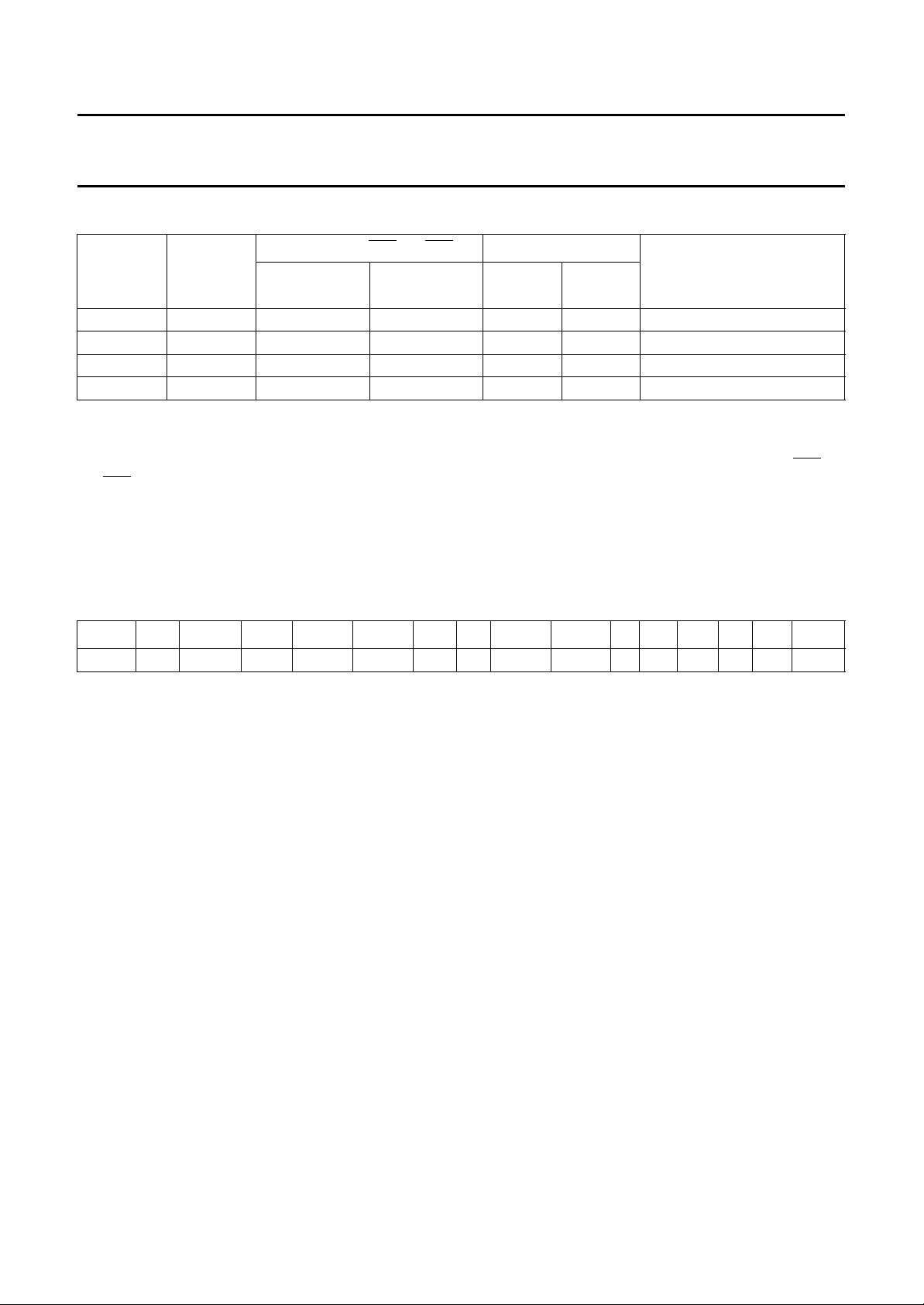
Low voltage 16-bit microcontroller P90CL301BFH (C100)
handbook, full pagewidth
peripheral
reset
RESET_AS
CPU-reset
LATCH
LATCH
CPU HALT
CLK
CLK
Watchdog reset
Fig.3 Reset circuitry.
instruction RESET
Watchdog reset
double bus fault
RESET
HALT
V
DD
external reset
capacitor
R
stin
RESETIN
MBG330
1996 Dec 11 14
Philips Semiconductors Preliminary specification
Low voltage 16-bit microcontroller P90CL301BFH (C100)
6.6 Clock generation
An external clock can be used with the P90CL301BFH.
The duty cycle of the external clock should be 50/50 ±5%
over the full temperature and voltage range.
For peripherals like Watchdog Timer, I2C-bus, PWM,
Timer and baud rate generator, a programmable prescaler
generates a peripheral clock FCLK.
handbook, full pagewidth
SYSCON
(IDL)
SYSCON
(PCLK3)
XTAL1
Idle mode
1/512
CLK
1/21
The prescaler is controlled by the System Control Register
(SYSCON). The internal clock is divided by a factor 2, 3, 4,
5, 6, 8 or 10 (function of bits PCLK0, PCLK1 and PCLK3;
see Table 15).
For the ADC a secondary peripheral clock FCLK2 is
derived from the peripheral clock by dividing it either by
4 or 2 (function of the bit PCLK2; see Table 14).
CPU
mode 0 clock
SYSCON
(PCLK2)
1/4 1/2
FCLK2
SYSCON
(PCLK0, 1)
ADC
1/2 1/3 1/4 1/5
FCLK
BRGSCON
I2C-BUS INTERFACES1CON
PWM0/PWM1
WATCHDOG
BCON
1 1/4
TIMER 0/TIMER 1PRESCALER
Fig.4 P90CL301BFH internal clock generation.
UART1
UART0
MGD781
1996 Dec 11 15
Philips Semiconductors Preliminary specification
Low voltage 16-bit microcontroller P90CL301BFH (C100)
6.7 Interrupt controller
An interrupt controller handles all internal and external
interrupts. It delivers the interrupt with the highest priority
level to the CPU. The following interrupt requests are
generated by the on-chip peripherals:
• I2C-bus
• UARTs: received data / transmitted data
• Timers: two flags for the timers T0 and T1
• ADC: analog-to-digital conversion completed.
The external interrupt requests are generated with the pins
NMIN and the seven external interrupts
6.7.1 I
The interrupt priority levels are programmable with a value
between 0 and 7. Level 7 has the highest priority, level 0
disables the corresponding interrupt source. In case of
interrupt requests of equal priority level at the same time a
hardware priority mechanism gives priority order as shown
in Table 16.
The execution of interrupt routines can be interrupted by
another interrupt request of a higher priority level. In 68070
mode (SYSCON bit IM = 1) when an interrupt is serviced
by the CPU, the corresponding level is loaded into the
Status Register. This prevents the current interrupt from
getting interrupted by any other interrupt request on the
same or a lower priority level. If IM is reset, priority level 7
will always be loaded into the Status Register and so the
current interrupt cannot be interrupted by an interrupt
request of a level less than 7.
Each on-chip peripheral unit including the eight interrupt
lines generate only auto-vectored interrupts. No
acknowledge is necessary. For external interrupts the
vectors 25 to 31 are used, for on-chip peripheral circuits a
second table of 7 vectors are used (57 to 63); see
Section 7.3.2.
NTERRUPT ARBITRATION
INT0 to INT6.
Table 16 Priority order
SIGNAL PRIORITY ORDER
NMIN highest
INT6
INT5
INT4
INT3
INT2
INT1
INT0
2
I
C-bus
ADC
UART1 receiver
UART1 transmitter
UART0 receiver
UART0 transmitter
Timer 1
Timer 0 lowest
6.7.2 EXTERNAL LATCHED INTERRUPTS
NMIN and INT0 to INT6 are 8 external interrupt inputs.
These pins are connected to the interrupt function only
when the corresponding bit in the SPCON control register
is set (see Section 8.2; Table 29). Seven interrupt inputs
INT0 to INT6 are edge sensitive on HIGH-to-LOW
transition and their priority levels are programmable.
The interrupt NMIN is non-maskable (except if it is
programmed as a port) and is also edge sensitive on
HIGH-to-LOW transition. The priority level of NMIN is fixed
to 7.
The external interrupts are controlled by the registers
LIR0 to LIR3; see Tables 17 and 18.
6.7.2.1 Latched Interrupt Registers (LIR0 to LIR3)
Table 17 Latched Interrupt Registers
ADDRESS REGISTER 7 6 5 43210
FFF 8101H LIR0 PIR1 IPL1.2 IPL1.1 IPL1.0 PIR0 IPL0.2 IPL0.1 IPL0.0
FFF 8103H LIR1 PIR3 IPL3.2 IPL3.1 IPL3.0 PIR2 IPL2.2 IPL2.1 IPL2.0
FFF 8105H LIR2 PIR5 IPL5.2 IPL5.1 IPL5.0 PIR4 IPL4.2 IPL4.1 IPL4.0
FFF 8107H LIR3 PIR7 1 1 1 PIR6 IPL6.2 IPL6.1 IPL6.0
1996 Dec 11 16
Philips Semiconductors Preliminary specification
Low voltage 16-bit microcontroller P90CL301BFH (C100)
Table 18 Description of LIR0 to LIR3 bits
BIT SYMBOL DESCRIPTION
7 and 3 PIRn Pending interrupt request. n = 0 to 7;
PIRn = 1, pending interrupt request for pin INTn. PIRn = 0 (default value after a CPU
reset), no pending interrupt. When a valid interrupt request has been detected this bit
is set. It is automatically reset by the interrupt acknowledge cycle from the CPU. It
can be reset by software by writing a logic 0, however writing a logic 1 has no effect
on the flag. To reset only one flag, a logic 0 should be written to the bit address and a
logic 1 to the other interrupt requests. The use of BCLR instruction should be
avoided (PIR7 is cleared when the pin NMIN is set HIGH)
6to4
2to0
IPLm.2 to IPLm.0
Interrupt priority level of pins
m=0to6.
INT0 to INT6 (fixed to ‘111B’ for NMIN in LIR3);
6.7.2.2 Pending Interrupt Flag Register (PIFR)
An additional register PIFR contains copies of the PIR flags. The PIF flags are set at the same time as the PIR flags when
an interrupt is activated, but these flags are not reset automatically during the interrupt acknowledge cycle. They can only
be cleared by software and keep a trace of the interrupt event. The detection of an external interrupt is indicated by the
corresponding PIF-bit being set to a logic 1.
INT7 corresponds to the interrupt NMIN;
Table 19 Pending Interrupt Flag Register (address FFFF 810F)
76543210
PIF7 PIF6 PIF5 PIF4 PIF3 PIF2 PIF1 PIF0
6.7.3 NOTE ON SIMULTANEOUS INTERRUPTS
If an internal interrupt is immediately followed by an
external interrupt (i.e. both interrupts occurring within 12
clock cycles) and both these interrupts have the same
interrupt level, then the CPU might hang up during the
acknowledge cycle of the internal interrupt.
In the interrupt controller a flag WIN is set for each interrupt
as soon as the interrupt is activated and will be reset when
an interrupt of higher priority occurs or during the
acknowledge cycle. The WIN flag is used to determine
which PIR flag should be reset.
A conflict occurs if within the interval starting at the CPU
sampling of the first internal interrupt and ending at the
acknowledge cycle, a second external interrupt resets the
WIN flag of the first interrupt (external interrupts have
higher priority than internal).
When the CPU acknowledges the first internal interrupt the
auto-vector acknowledge signal cannot be asserted as its
WIN flag was reset, and the CPU hangs up.
This situation can be solved by using the bus time-out
counter controlled by the System Control Register
(SYSCON) with the bits WD and WDSC set. In the case of
hang-up an internal bus error condition will be asserted
after 16 clocks and the CPU will execute the exception
SPURIOUS INTERRUPT at vector 60H. In the exception
service routine the interrupt flags PIR should be polled to
detect which interrupts caused the conflict, the
corresponding PIR flags should be cleared by software
and a call to the interrupt routines executed.
1996 Dec 11 17

Philips Semiconductors Preliminary specification
Low voltage 16-bit microcontroller P90CL301BFH (C100)
6.8 Power reduction modes
The P90CL301BFH supports three power reduction
modes. A Power-down mode where the clock is frozen, a
Standby mode where only the CPU is stopped, and an Idle
mode where the external clock is divided by 512
(see Fig.4).
6.8.1 P
OWER-DOWN MODE
The Power-down operation freezes the oscillator. It can
only be activated by setting the PD bit in the SYSCON
register and thereafter execute the STOP instruction.
The instruction flow to enter the Power-down mode is:
BSET #PD, SYSCON
STOP #$2700.
In this state all the register contents are preserved.
The CPU remains in this state until an internal reset occurs
or a LOW level is present on any of the external interrupt
pins INT0 to INT6 or NMIN. If the wake-up is done via an
external interrupt, the processor will first execute an
external interrupt of level 7. If the IPL level in the LIR
register is set to 7, a second interrupt of level 7 will be
executed. It is preferable to set the IPL to 0.
In Power-down mode VDD may be reduced to minimize
power consumption. However, the supply voltage must not
be reduced until Power-down mode is active, and must be
restored before a external reset or an interrupt is activated.
In case of an external reset, the pin should be held active
until the external oscillator has restarted and stabilized.
In case of an external interrupt wake-up, anyINTn or NMIN
pin should go LOW and the corresponding bit ESn
(n = 0 to 7) in register SPCON should be set. If the DOFF
bit in the SYSCON is not set, an internal delay counter
ensures that the internal clock is not active before
1536 clock cycles. After that time the oscillator is stable
and normal exception processing can be executed.
The PD bit is cleared automatically during the wake-up.
6.8.2 S
TANDBY MODE
When the STBY bit in the SYSCON register is set, the
CPU clock is stopped and the status of the processor is
frozen, however, the clocks of all other on-chip peripherals
are still running at the nominal frequency; these
peripherals are:
• Timers
• External and internal interrupts
• UARTs and baud rate generator
• I2C-bus interface
• Watchdog Timer
• PWMs
• ADC.
The CPU exits this mode when an internal or external
interrupt is activated, and proceeds with the normal
program execution.
For minimum power consumption internal pull-ups on
address and data buses can be switched on by setting the
control bit BPE in the SYSCON register. The pull-ups
should be switched off in normal mode if not needed.
6.8.3 I
DLE MODE
In the Idle mode the crystal or external clock is divided by
a factor 512. The current is reduced drastically but the
controller continues to operate. This mode is entered by
setting the bit IDL in the SYSCON register. The next
instruction will be executed at a slower speed. To return to
normal mode the IDL bit should be reset.
It should be noted that all peripheral functions are also
slowed down, and some cannot be used normally, for
example UART, I2C-bus, ADC and PWM.
The Power-down mode can also be entered from the Idle
mode. After a wake-up the controller restarts in Idle mode.
In order to have a fast start-up the DOFF bit should be set,
switching off the delay counter and enabling the immediate
clocking and restart of the controller.
For minimum power consumption during Power-down
mode, the address and data pins should be pulled HIGH
externally or bit BPE in register SYSCON should be set
(i.e. internal pull-ups enabled).
1996 Dec 11 18

Philips Semiconductors Preliminary specification
Low voltage 16-bit microcontroller P90CL301BFH (C100)
7 CPU FUNCTIONAL DESCRIPTION
7.1 General
The CPU of the P90CL301BFH is software compatible
with the Motorola MC68000, hence programs written for
the MC68000 will run on the P90CL301BFH without
modifications. However, for certain applications the
following differences between processors should be
noted:
• Differences exist in the address/bus error exception
processing since the P90CL301BFH can provide full
error recovery.
• The timing is different for the P90CL301BFH due to a
new internal architecture and technology.
The instruction execution timing is different for the same
reasons.
Table 20 Format of the Status Register and description of the bits; r = reserved
15 14 13 12 11 10 9 8 7 6 5 4 3 2 1 0
T − S −−12 11 10 −−− XNZVC
Trace mode r Supervisor r Interrupt mask r Extend Negative Zero Overflow Carry
7.2 Programming model and data organization
The programming model is identical to that of the
MC68000 (see Fig.5), with seventeen 32-bit registers, a
32-bit Program Counter and a 16-bit Status Register.
The eight data registers (D0 to D7) are used for byte, word
and long-word operations. The Address Registers
(A0 to A6) and the System Stack Pointer A7 can be used
as software stack pointers and base address registers. In
addition, these registers can be used for word and
long-word address operations. All seventeen registers can
be used as index registers.
The P90CL301BFH supports 8, 16 and 32-bit integers as
well as BCD data and 32-bit addresses. Each data type is
arranged in the memory as shown in Fig.6.
1996 Dec 11 19
Philips Semiconductors Preliminary specification
Low voltage 16-bit microcontroller P90CL301BFH (C100)
31 16 15 8 7 0
dbook, full pagewidth
DO
D1
D2
D3
D4
D5
D6
D7
Eight
Data
Registers
31 16 15 0
USER STACK POINTER
SUPERVISOR STACK POINTER
31 0
15 8 7 0
USER
BYTE
MCD504
SYSTEM
BYTE
A0
A1
A2
A3
A4
A5
A6
A7
Seven
Address
Registers
Two Stack
Pointers
Program
Counter
Status
Register
Fig.5 Programming model.
1996 Dec 11 20
Philips Semiconductors Preliminary specification
Low voltage 16-bit microcontroller P90CL301BFH (C100)
bit
(a) Bit data (1 Byte = 8 bits).
15 14 13 12 11 10 9 8 7 6 5 4 3 2 1 0bit
MSB BYTE 0
BYTE 2
1514131211109876543210bit
MSB WORD 0
1514131211109876543210bit
MSB HIGH ORDER
LONG WORD 0
LONG WORD 1
LONG WORD 2
LSB
(b) Integer data (1 Byte = 8 bits).
WORD 1
WORD 2
(c) Word data (16 bits).
276543 10
LOW ORDER LSB
HIGH ORDER
LOW ORDER
HIGH ORDER
LOW ORDER
BYTE 1
BYTE 3
LSB
(d) Long-word data (32 bits).
1514131211109876543210bit
MSB HIGH ORDER
1514131211109876543210bit
MSB LSB
ADDRESS 0
ADDRESS 1
ADDRESS 2
(e) Addresses (1 address =32 bits).
BCD 0 BCD 1
BCD 4 BCD 5
(f) BCD data (2 BCD digits = 1 Byte).
Fig.6 Memory data organization.
1996 Dec 11 21
LOW ORDER LSB
HIGH ORDER
LOW ORDER
HIGH ORDER
LOW ORDER
BCD 2 BCD 3
BCD 6 BCD 7
MCD505

Philips Semiconductors Preliminary specification
Low voltage 16-bit microcontroller P90CL301BFH (C100)
7.3 Processing states and exception processing
The P90CL301BFH operates with a maximum internal
clock frequency of 27 MHz down to static operation. Each
clock cycle is divided into 2 states. A non-access machine
cycle has 3 clock cycles or 6 states (S0 to S5). A minimum
bus cycle normally consists of 3 clock cycles (6 states).
When DTACK is not asserted, indicating that data transfer
has not yet been terminated, wait states (WS) are inserted
in multiples of 2.
The CPU is always in one of the four processing states:
• Normal
• Exception
• Halt
• Stopped.
The Normal processing state is associated with instruction
execution; the memory references fetch instructions or
load/save results. A special case of the Normal state is the
Stopped state which is entered by the processor when a
STOP instruction is executed. In this state the CPU does
not make any further memory references.
The Exception state is associated with interrupts, trap
instruction, tracing and other exceptional conditions.
The exception may be generated internally by an
instruction or by any unusual condition arising during the
execution of an instruction. Externally, exception
processing can be forced by an interrupt or by reset.
The halted processing state is an indication of a
catastrophic hardware failure. For example, if during
exception processing of a bus error another bus error
occurs, the CPU assumes that the system is unusable and
halts. Only an external reset can restart a halted
processor. Note that a CPU in the stopped state is not in
the halted state or vice versa.
The Supervisor can work in the User or Supervisor state
determined by the state of bit S in the Status Register.
Accesses to the on-chip peripherals are achieved in the
Supervisor state.
7.3.1 REFERENCE CLASSIFICATION
When the processor makes a reference, it classifies the
kind of reference being made, using the encoding of the
three function code internal lines. This allows external
translation of addresses, control of access, and
differentiation of special processor states, such as
interrupt acknowledge. Table 21 shows the classification
of references.
Table 21 Reference classification
FUNCTION CODE
FC2 FC1 FC0
0 0 0 unassigned
0 0 1 User Data
0 1 0 User Program
0 1 1 unassigned
1 0 0 unassigned
1 0 1 Supervisor Data
1 1 0 Supervisor Program
1 1 1 interrupt acknowledge
7.3.2 E
Exception vectors are memory locations from where the
CPU fetches the address of a routine that will handle that
exception. All exception vectors are 2 words long, except
for the reset vector which consists of 4 words, containing
the PC and the SSP. All exception vectors are in the
Supervisor Data space.
A vector number is an 8-bit number which, multiplied by 4,
gives the address of an exception vector. Vector numbers
are generated internally. The memory map for the
exception vectors is shown in the Table 22.
XCEPTION VECTORS
REFERENCE CLASS
All exception processing is performed in the Supervisor
state once the current contents of the Status Register has
been saved. Then the exception vector number is
determined and copies of the Status Register, the program
counter and the format/vector number are saved on the
Supervisor stack using the Supervisor Stack Pointer
(SSP). Finally the contents of the exception vector location
is fetched and loaded into the Program Counter (PC).
1996 Dec 11 22
Philips Semiconductors Preliminary specification
Low voltage 16-bit microcontroller P90CL301BFH (C100)
Table 22 Exception vector assignment
VECTOR NO. DECIMAL HEX ASSIGNMENT
0 0 000 reset: initial SSP
− 4 004 reset: initial PC
2 8 008 bus error
3 12 00C address error
4 16 010 illegal instruction
5 20 014 zero divide
6 24 018 CHK instruction
7 28 01C TRAPV instruction
8 32 020 privilege violation
9 36 024 trace
10 40 028 line 1010 emulator
11 44 02C line 1111 emulator
(1)
12
(1)
13
14 56 038 format error
15 60 03C uninitialized interrupt vector
16 to 23
(1)
24 96 060 spurious interrupt
25 100 064 level 1 external interrupt auto-vector
26 104 068 level 2 external interrupt auto-vector
27 108 06C level 3 external interrupt auto-vector
28 112 070 level 4 external interrupt auto-vector
29 116 074 level 5 external interrupt auto-vector
30 120 078 level 6 external interrupt auto-vector
31 124 07C level 7 external interrupt auto-vector
32 to 47 128 to 191 080 to 0BF TRAP instruction vectors
48 to 56
(1)
57 228 0E4 level 1 on-chip interrupt auto-vector
58 232 0E8 level 2 on-chip interrupt auto-vector
59 236 0EC level 3 on-chip interrupt auto-vector
60 240 0F0 level 4 on-chip interrupt auto-vector
61 244 0F4 level 5 on-chip interrupt auto-vector
62 248 0F8 level 6 on-chip interrupt auto-vector
63 252 0FC level 7 on-chip interrupt auto-vector
64 to 255 256 to 1023 100 to 3FF reserved
48 030 unassigned, reserved
52 034 unassigned, reserved
64 to 95 040 to 05C unassigned, reserved
192 to 227 0C0 to 0E3 reserved
Note
1. Vectors 12, 13, 16 to 23 and 48 to 56 are reserved for future enhancements.
1996 Dec 11 23

Philips Semiconductors Preliminary specification
Low voltage 16-bit microcontroller P90CL301BFH (C100)
7.3.3 INSTRUCTION TRAPS
Traps are exceptions caused by instructions arising from
CPU recognition of abnormal conditions during instruction
execution or from instructions whose normal behaviour is
to cause traps.
Some instructions are used specifically to generate traps.
The TRAP instruction always forces an exception and is
useful for implementing system calls for User Programs.
The TRAPV and CHK instructions force an exception if the
User Program detects a run-time error, possibly an
arithmetic overflow or a subscript out of bounds.
The signed divide (DIVS) and unsigned divide (DIVU)
instructions will force an exception if a divide-by-zero
operation is attempted.
7.3.4 I
Illegal instruction is the term used to refer to any word that
is not the first word of a legal instruction. During execution,
if such an instruction is fetched an illegal exception occurs.
Words with bits 15 to 12 equal to ‘1010’ or ‘1111’ are
defined as unimplemented instructions and separate
exception vectors are allocated to these patterns for
efficient emulation. This facility means the operating
system can detect program errors, or can emulate
unimplemented instructions in software.
LLEGAL AND UNIMPLEMENTED INSTRUCTIONS
The trace facility uses the T-bit in the Supervisor part of the
Status Register. If the T-bit is cleared, tracing is disabled
and instructions are executed normally. If the T-bit is set at
the beginning of the execution of an instruction, a trace
exception will be generated once the instruction has been
executed. If the instruction is not executed, either because
of an interrupt, or because the instruction is illegal or
privileged, the trace exception does also not occur if the
instruction is aborted by a reset, bus error, or address error
exception. If the instruction is executed, and an interrupt is
pending, the trace exception is processed before the
interrupt. If the execution of an instruction forces an
exception, the forced exception is processed before the
trace exception.
As an extreme illustration of the above rules, consider the
arrival of an interrupt during the execution of a TRAP
instruction, while tracing is enabled. First the trap
exception is processed, followed by the trace exception,
and finally the interrupt handling routine.
7.5 Stack format
The stack format for exception processing is similar to the
MC68010 although the instruction stored is not the same,
due to the different architecture. To handle this format the
P90CL301BFH differs from the MC68000 in that:
7.3.5 P
To provide system security, various instructions are
privileged and any attempt to execute one of the privileged
instruction while the CPU is in the User state provokes an
exception. The privileged instructions are:
• STOP
• RESET
• RTE
• MOVE to SR
• AND (word) immediate to SR
• EOR (word) immediate to SR
• OR (word) immediate to SR
• MOVE to USP.
7.4 Tracing
The CPU includes a facility to trace instructions one by one
to assist in program development. In the trace state, after
each instruction is executed, an exception is forced so that
the debugging program can monitor execution of the
program under test.
RIVILEGE VIOLATIONS
• The stack format is changed.
• The minimum number of words put into or restored from
stack is 4 (MC68010 compatible, not 3 as with the
MC68000).
• The RTE instruction decides (with the aid of the 4 format
bits) whether or not more information has to be restored
as follows:
– The P90CL301BFH long format is used for bus errors
and address error exceptions.
– All other exceptions use the short format.
• If another format code, other than those listed above, is
detected during the restored action, a FORMAT ERROR
occurs.
If the user wants to finish the instruction in which the bus
or address error occurred, the P90CL301BFH format must
be used on RTE. If no changes to the stack are required
during exception processing, the stack format is
transparent to the user.
1996 Dec 11 24
Philips Semiconductors Preliminary specification
Low voltage 16-bit microcontroller P90CL301BFH (C100)
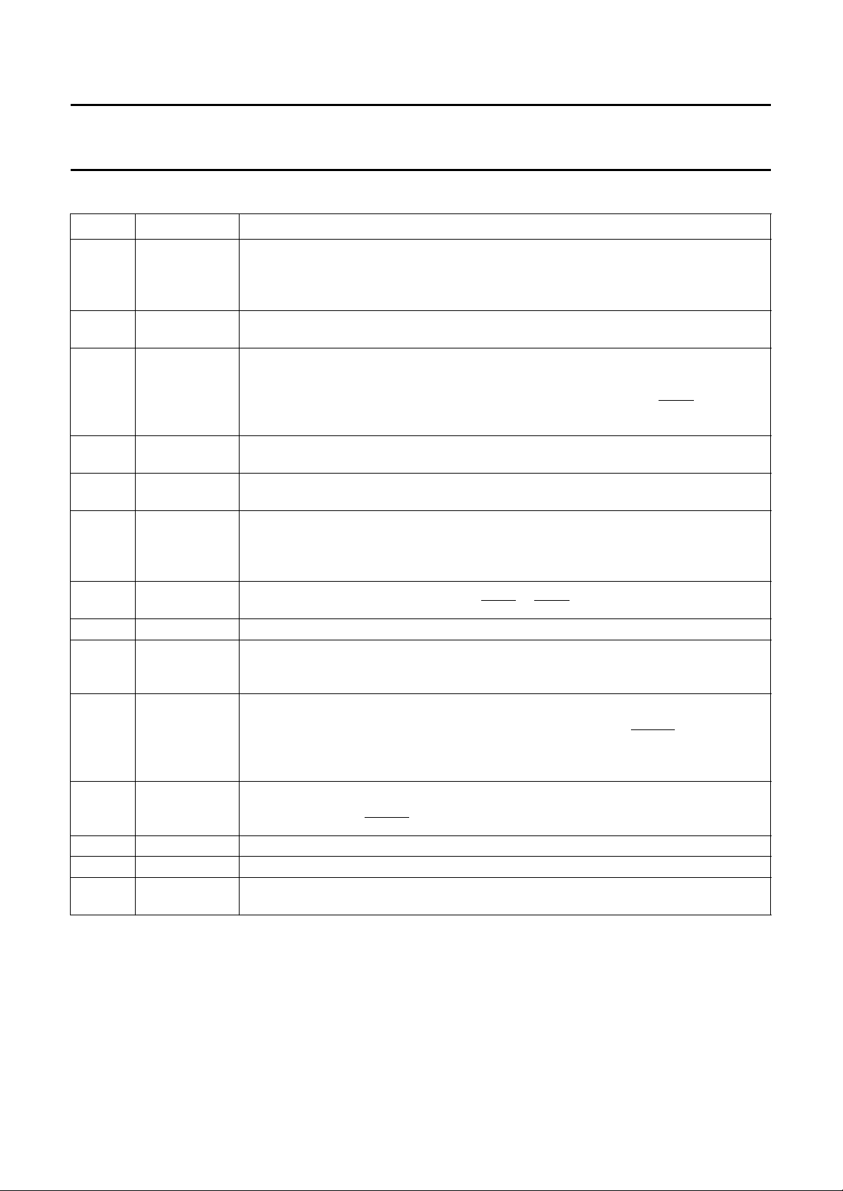
book, full pagewidth
SP
Long
Stack
Format
SR
PCH
PCL
FORMAT (4 bits) BASE VECTOR ADDRESS
SSW
MM
INTERNAL INFORMATION
INTERNAL INFORMATION
TPDH
TPDL
TPFH
TPFL
DBINH
DBINL
IR
IRC
INTERNAL INFORMATION
MBG426
Short
Stack
Format
Fig.7 Stack format; see Table 23.
Table 23 Description of the stack format
SYMBOL DESCRIPTION
SR Status Register.
PCH/PCL Program Counter High/Low Word.
FORMAT Indicating either a short stack (only the first four words), or the long for bus and address error
exceptions.
BASE VECTOR
ADDRESS
The base vector address of the exception in the vector table; e.g. 8 for a bus error and 12 for
an address error.
SSW Special Status Word.
MM Current Move Multiple Mask.
TPDH/TPDL In the event of faulty write cycle, the data can be found here.
TPFH/TPFL The address used during the faulty bus cycle.
DBINH/DBINL Data that has been read prior to the faulty bus cycle can in some cases be found here.
IR Holds the present instruction executed.
IRC Holds either the present instruction executed or the prefetched instruction.
1996 Dec 11 25

Philips Semiconductors Preliminary specification
Low voltage 16-bit microcontroller P90CL301BFH (C100)
7.6 CPU interrupt processing
The general interrupt handling mechanism is described in
Section 6.7. An interrupt controller handles all interrupts,
resolves the priority problem and passes the highest level
interrupt to the CPU.
The CPU interrupt handling follows the same basic rules
as in the MC68000. However, some remarks must be
made:
• Interrupts with a priority level equal to or lower than the
current priority level will not be accepted.
• During the acknowledge cycle of an interrupt, the IPL
bits of the Status Register are set to the priority of the
acknowledged interrupt or to 7. An exception occurs
when bit IM = 0 (SYSCON bit 5). In this case level 7 is
loaded into the Status Register (see Section 6.4;
Table 14).
If the priority level of the pending interrupt is greater than
the current processor priority then:
• The exception processing sequence is started
• A copy of the Status Register is saved
• The privilege level is set to Supervisor state
• Tracing is suppressed
• The priority level of the processor is set to that of the
interrupt being acknowledged or to 7 depending on the
IM flag in the System Control Register.
As all P90CL301BFH interrupts are auto-vectored, the
processor internally generates a vector number
corresponding to the interrupt level number.
The processor starts normal exception processing by
saving the format word, program counter and Status
Register on the Supervisor stack. The value of the vector
in the format word is an internally generated vector number
multiplied by 4 (format is all zeros). The program counter
value is the address of the instruction that would have
been executed if the interrupt had not been present. Then
the interrupt vector contents are fetched and loaded into
the program counter. The interrupt handling routine starts
with normal instruction execution.
7.7 Bus arbitration
HALT pin is held LOW with RESET HIGH the CPU
If the
will stop after completion of the current bus cycle. As long
as HALT is LOW, all control signals are inactive and all
3-state lines are placed in the high-impedance state. If the
HALT pin is held LOW during the transfer of a word in 8-bit
mode, the CPU will continue the transfer of the two bytes
before it halts.
The processor then gets the vector number from the
interrupting device, classifies it as an interrupt
acknowledge and displays the interrupt level number
being acknowledged on the internal address bus.
1996 Dec 11 26

Philips Semiconductors Preliminary specification
Low voltage 16-bit microcontroller P90CL301BFH (C100)
8 PORTS
For general purpose input/output operations the following
ports can be used:
• 16-bit bidirectional port lines P15 to P0 composed of two
8-bit ports PL (P7 to P0) and PH (P15 to P8)
• 8-bit port lines SP7 to SP0.
All port pins are multiplexed with other functions, but each
one can be individually switched to the port function by
setting the corresponding bit in the Port P Control Register
(PCON) for ‘port Pn’ and Port SP Control Register
(SPCON) for ‘port SPn’.
The port P7 to P0 is multiplexed with the data bus
D15 to D8 and is selected by the pin BSIZE.
8.1 Port P Control Register (PCON)
The port Pn is controlled via the Port P Control Register (PCON). The register PCON is only reset by an external reset,
and not by the RESET instruction. The port latches are accessed through the registers PRL and PRH.
Table 24 Port P Control Register (address FFFF 8503H)
76543210
E15 E14 E13 E12 E11 E10 E9 E8
Each port pin consists of a latch, an output driver with
pull-ups and an input buffer.
To use the port as input the port latch should be written
with a logic 1. This means only a weak pull-up is on and
can be overwritten by an external source logic 0.
When outputting a logic 1, a strong pull-up is turned on
only for 1 clock period, and then only the weak pull-up
maintains the HIGH level. In read mode, two different
internal addresses correspond to the port latch or the port
pin.The port values are read via register PPL and PPH.
After reset all ports are initialized as input, and the pins are
connected to the port latch with exception for the pin
NMIN/SP7 which is connected to the interrupt block.
Table 25 Description of PCON bits
BIT SYMBOL DESCRIPTION
7 to 0 E15 to E8 If En = 0, then ‘port Pn’ is enabled; if En = 1, then the alternate function is enabled;
n = 8 to 15. The default value after reset is logic 0.
8.1.1 P
Table 26 Port P Latch least significant byte (PRL; address FFFF 8505H)
Table 27 Port Latches High most significant byte (PRH; address FFFF 8509H)
ORT PLATCHES
76543210
P7 P6 P5 P4 P3 P2 P1 P0
76543210
P15 P14 P13 P12 P11 P10 P9 P8
1996 Dec 11 27
Philips Semiconductors Preliminary specification
Low voltage 16-bit microcontroller P90CL301BFH (C100)
8.2 Port SP Control Register (SPCON)
The special ports SPn (SP0 to SP7) consist of 8 I/O lines and are controlled via the two registers SPCON and SPR. The
registers SPCON and SPR are reset by a peripheral reset. The port latch is accessed through the register SPR.
8.2.1 P
Table 28 Port SP Control Register (address FFFF 8109H)
Table 29 Description of SPCON bits
8.2.2 P
Table 30 Port SP latch (FFFF 810BH)
8.2.3 ALTERNATIVE FUNCTIONS FOR PORTS P AND SP
Table 31 Alternative functions for P0 to P15 and
Functions within brackets are parallel functions.
ORT SP CONTROL REGISTER (SPCON)
76543210
ES7 ES6 ES5 ES4 ES3 ES2 ES1 ES0
BIT SYMBOL DESCRIPTION
7 to 0 ES7 to ES0 If ESn = 0, then ‘port SPn’ is enabled; if ESn = 1, then the alternate function is enabled;
n = 0 to 7. The default value after reset is logic 0, except for ES7 which is set at reset.
ORT SP LATCH (SPR)
76543210
SP7 SP6 SP5 SP4 SP3 SP2 SP1 SP0
SP0 to SP7 pins
PORT PIN ALTERNATE FUNCTION
P0 D8
P1 D9
P2 D10
P3 D11
P4 D12
P5 D13
P6 D14
P7 D15
P8 PWM0 (CP0)
P9 PWM1 (CP1)
P10 SCL
P11 SDA
PORT PIN ALTERNATE FUNCTION
P12 ADC0
P13 ADC1
P14 ADC2
P15 ADC3
SP0 RX1/
SP1 TX1/
SP2 RX0/
SP3 TX0/
SP4
SP5
SP6
SP7 NMIN
INT0
INT1 (CLK0)
INT2 (CP2)
INT3 (CP3)
INT4 (CP4)
INT5 (CP5)
INT6 (CLK1)
1996 Dec 11 28
 Loading...