

Philips p90ce201 DATASHEETS

INTEGRATED CIRCUITS
DATA SH EET
P90CE201
16-bit microcontroller
Product specification
File under Integrated Circuits, IC21
August 1993

Philips Semiconductors Product specification
16-bit microcontroller P90CE201
CONTENTS
1 FEATURES
2 GENERAL DESCRIPTION
3 ORDERING INFORMATION
4 PINNING INFORMATION
4.1 Pinning
4.2 Pin description
5 CPU FUNCTIONAL DESCRIPTION
5.1 General
5.2 5.2 Programming model and data organization
5.3 Internal and external operation
5.4 Processing states and exception processing
5.5 Stack format
5.6 CPU interrupt processing
6 SYSTEM CONTROL
6.1 Memory mapping
6.2 Interrupt controller
6.3 System Control Registers
6.4 Reset
6.5 Clock circuitry
7 INSTRUCTION SET
7.1 Addressing modes
7.2 Instruction timing
8I
8.1 General
8.2 I2C-bus interface registers
9 UART SERIAL INTERFACE
9.1 General
9.2 Operating modes
9.3 UART registers
2
C-BUS INTERFACE
10 8-BIT GENERAL PORT
10.1 8-bit General Port registers
11 8-BIT AUXILIARY PORT
11.1 8-bit Auxiliary Port registers
12 WATCHDOG TIMER
13 TIMERS
13.1 General
13.2 Timer operating modes
13.3 Timer registers
14 ELECTROMAGNETIC COMPATIBILITY
(EMC) IMPROVEMENTS
15 ELECTRICAL SPECIFICATIONS
15.1 Limiting values
15.2 DC Characteristics
15.3 AC Characteristics
16 REGISTER MAP
17 PACKAGE OUTLINE
18 SOLDERING
18.1 Introduction
18.2 Reflow soldering
18.3 Wave soldering
18.4 Repairing soldered joints
19 DEFINITIONS
20 LIFE SUPPORT APPLICATIONS
21 PURCHASE OF PHILIPS I2C COMPONENTS
August 1993 2

Philips Semiconductors Product specification
16-bit microcontroller P90CE201
1 FEATURES
• CMOS technology
• Full 68000 software compatibility
• 32-bit internal structure
• 16-bit internal data transfer
• 8-bit access to external ROM/RAM
• External addressing range 16 Mbytes for ROM and
16 Mbytes for RAM
• Unused address pins can be used as quasi-bidirectional
ports
• On-chip address decoder for ROM/RAM
• 8 edge triggered programmable interrupts that can also
be used as quasi-bidirectional ports
• Reset control
• Built-in clock generator
2
• 2 fully independent fast I
• UART serial interface (4 modes)
• 3 fully independent 16-bit timers
• Watchdog timer
• 8-bit quasi-bidirectional port, 4-bits with high drive
capability
• EMC optimized layout and pinning
• 64-pin QFP package
C-bus serial interfaces
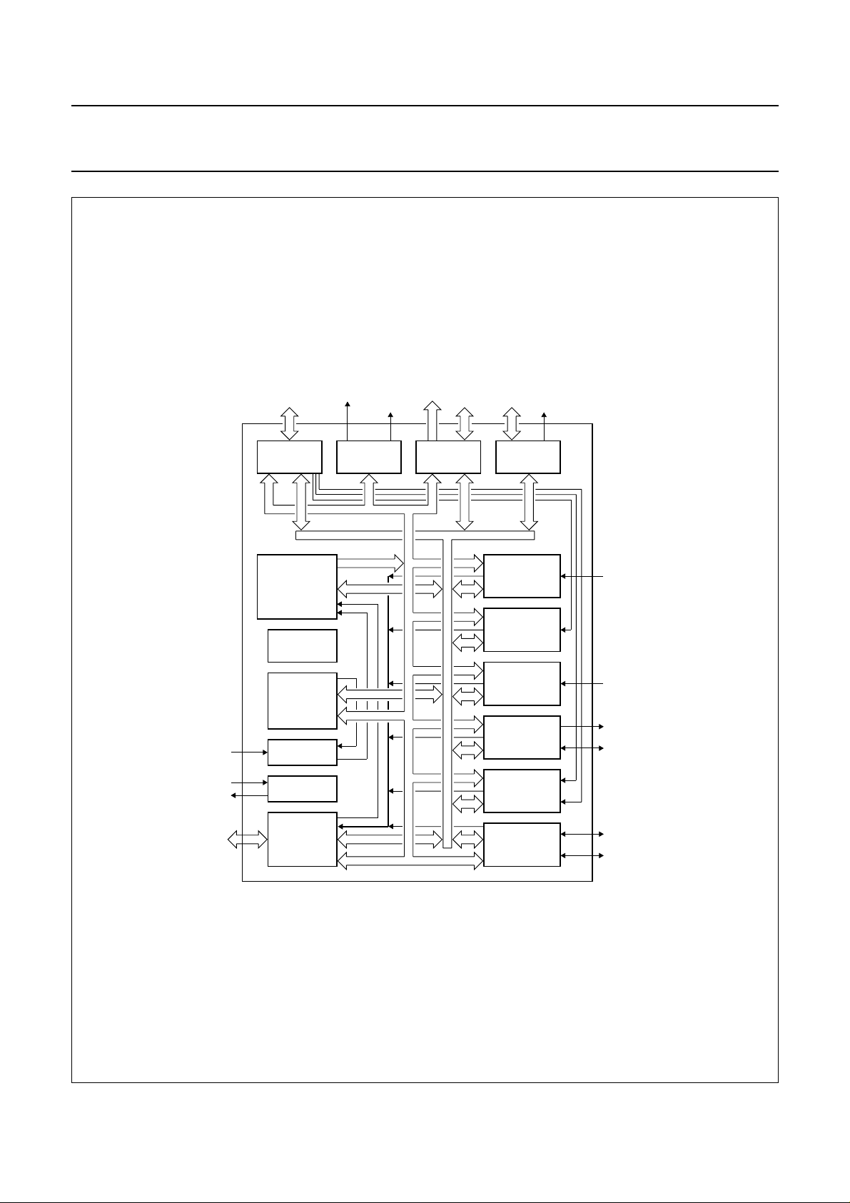
2 GENERAL DESCRIPTION
The P90CE201 is a member of the P9XCXXX family of
highly integrated 16-bit microcontrollers for use in a wide
variety of applications. It is fully software compatible with
the 68070/68000. The complete set of system functions
available on the chip results in reduced system cost.
Additionally, its modular design concept permits future
extension to the family.
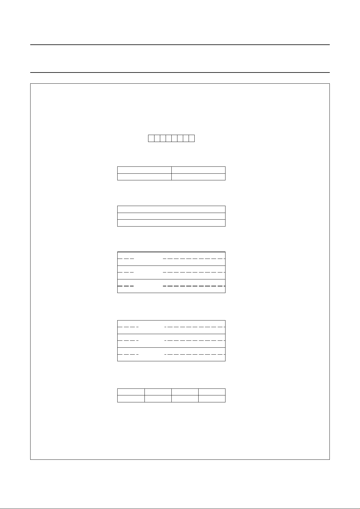
3 ORDERING INFORMATION
EXTENDED
TYPE NUMBER
P90CE201AEB 64 QFP plastic SOT319
Note
1. SOT319-2; 1996 November 28.
August 1993 3
PINS PIN POSITION MATERIAL CODE
PACKAGE CLOCK
FREQUENCY
(1)
TEMPERATURE RANGE
(MHz)
24.0 −25 to 85
(°C)
Philips Semiconductors Product specification
16-bit microcontroller P90CE201
RESET
XTAL1
XTAL2
GP0-GP7
(1)
PORT
CPU
SYSTEM
CONTROL
WATCHDOG
TIMER
RESET
LOGIC
CLOCK
CSRAMN
ADDRESS
DECODER
CSROMN
OCA (31 : 0)
A0-A15
ADDRESS
BUFFER
A16-A23
D0-D7
INTERFACE
OCD (15 : 0)
TIMER 0
TIMER 1
TIMER 2
UART
I C 1
R/WN
DATA
T0
T2
TXD
RXD
2
INTN0 INTN7
INTERRUPT
CONTROLLER
1. The General Port lines GP5, GP6 and GP7 have alternate functions for Timer 1, SCL1 and SDA1
respectively; see Table 1.
Fig.1 Block diagram
August 1993 4
2
I C 2
SCL2
SDA2
MLB015

Philips Semiconductors Product specification
16-bit microcontroller P90CE201
4 PINNING INFORMATION
4.1 Pinning
DD2
V
RESET
T0
27
T2
LP0/INTN0
56
55
28
29
A7
A13
54
53
52
V
51
SS2
CSRAMN
50
49
D3
48
D2
47
D4
46
D1
45
D5
44
D0
43
D6
42
A0
D7
41
40
A1
39
A2
38
A10
A3
37
CSROMN
36
35
A4
34
A11
33
A5
30
31
32
A8
A6
MLB003
A9
handbook, full pagewidth
RXD
SDA2
SCL2
GP7/SDA1
GP6/SCL1
GP0
GP1
GP2
GP3
GP4
GP5/T1
A23/AP7
A22/AP6
A21/AP5
A20/AP4
XTAL2
XTAL1
V
DD1
V
SS1
TXD
LP6/INTN6
LP7/INTN7
64
63
62
1
2
3
4
5
6
7
8
9
10
11
12
13
14
15
16
17
18
19
20
21
R/WN
A19/AP3
LP5/INTN5
61
22
23
A18/AP2
A16/AP0
LP4/INTN4
60
P90CE201
24
A17/AP1
LP2/INTN2
LP3/INTN3
59
58
25
26
A15
A14
LP1/INTN1
57
A12
Fig.2 Pin configuration for QFP64.
August 1993 5

Philips Semiconductors Product specification
16-bit microcontroller P90CE201
4.2 Pin description Table 1 QFP64 package.
MNEMONIC TYPE PIN NO. FUNCTION
RXD I/O 1 Receive Data. RXD is the data input for the UART interface.
SDA2 I/O 2 Serial Data 2 (open drain). SDA2 is the data signal for the second
SCL2 I/O 3 Serial Clock 2 (open drain). SCL2 is the clock signal for the second
GP7/SDA1
GP6/SCL1
GP0
GP1
GP2
GP3
GP4
GP5/T1
A23/AP7
to
I/O 4
5
6
7
8
9
10
11
I/O 12 to 15, 21,
22, 24, 23
A16/AP0
A15 to A0 O 25, 26, 28, 27,
34, 38, 32, 30,
29, 31, 33, 35,
37, 39, 40, 42
XTAL2 O 16 Oscillator output. Not connected if an external clock generator is used.
XTAL1 I 17 Oscillator input. XTAL1 can also be used as an external clock input if
V
V
DD1
SS1
− 18 Supply voltage. For internal logic, address bus, data bus, RWN,
− 19 Ground. For internal logic, address bus, data bus, RWN, CSRAMN,
R/WN O 20 Read (active HIGH)/Write (active LOW). This controls the direction of
CSROMN O 36 Chip Select ROM (active LOW). This signal selects external ROM.
D0 to D7 O 44, 46, 48, 49,
47, 45, 43, 41
CSRAMN O 50 Chip Select RAM (active LOW). This signal enables external RAM.
V
V
SS2
DD2
− 51 Ground. For all other periphery pins (quiet port).
− 52 Supply voltage. For all other periphery pins (quiet port).
RESET I 53 Reset (active HIGH). Input pin for an external reset.
T0 I 54 Timer 0. Input pin for cycle and event counting using Timer 0.
T2 I 55 Timer 2. Input pin for cycle and event counting using Timer 2.
2
I
C-bus serial interface.
2
C-bus serial interface.
I
General Purpose Port (active HIGH, 3-state). The alternative functions
are as follows. SCL1 is the clock signal for the first I
2
C-bus serial
interface. SDA1 is the data signal for the first I2C-bus serial interface.
T1 is the input pin for Timer 1.
Address Bus. Upper 8-bits of the address bus (A23 to A16). The unused
address bits can be selected as a quasi-bidirectional port (AP).
Address Bus. Lower 16-bits of the address bus.
an external clock generator is used.
CSRAMN, CSROMN, XTAL1 and XTAL2.
CSROMN, XTAL1 and XTAL2.
data flow.
Data Bus. 8-bit data bus.
August 1993 6

Philips Semiconductors Product specification
16-bit microcontroller P90CE201
MNEMONIC TYPE PIN NO. FUNCTION
LP0/INTN0
LP1/INTN1
LP2/INTN2
LP3/INTN3
LP4/INTN4
LP5/INTN5
LP6/INTN6
LP7/INTN7
TXD O 64 Transmit Data. TXD is the data output for the UART serial interface.
I/O 56
57
58
59
60
61
62
63
Latched Interrupt inputs (active LOW). A LOW level of ≥ 1 clock pulse
will be stored as a pending interrupt request. Priority levels are
programmable. Unused interrupt inputs can be used as a
quasi-bidirectional port (LP).
August 1993 7

Philips Semiconductors Product specification
16-bit microcontroller P90CE201
5 CPU FUNCTIONAL DESCRIPTION
5.1 General
The CPU of the P90CE201 is software compatible with the
68000, consequently programs written for the 68000 will
run on the P90CE201 unchanged. However, for certain
applications the following differences between the
processors should be noted:
• The initialization of the System Control Registers.
• Differences exist in the address error exception
processing since the P90CE201 can provide full error
recovery.
• The timing is different because of the P90CE201’s new
architecture and technology. The instruction execution
timing is completely different for the same reason.
31 16 15 8 7 0
handbook, full pagewidth
5.2 5.2 Programming model and data organization
The programming model is identical to that of the 68000
and is shown in Fig.3. It contains seventeen 32-bit
registers, a 32-bit Program Counter and a 16-bit Status
Register. The first eight registers (D0 to D7) are used as
data registers for byte, word and long-word operations.
The second group of registers (A0 to A6) and the System
Stack Pointer (A7) can be used as software stack pointers
and base address registers. In addition, these registers
can be used for word and long-word address operations.
All seventeen registers can be used as Index Registers.
The P90CE201 supports 8, 16 and 32-bit integer data,
BCD data 32-bit addresses. Each data type is arranged in
memory as shown in Fig.4.
DO
D1
D2
Eight
D3
Data
D4
Registers
D5
D6
D7
31 16 15 0
USER STACK POINTER
SUPERVISOR STACK POINTER
31 0
MCD504
Fig.3 Programming model.
August 1993 8
15 8 7 0
SYSTEM
BYTE
USER
BYTE
A0
A1
A2
A3
A4
A5
A6
A7
Seven
Address
Registers
Two Stack
Pointers
Program
Counter
Status
Register
Philips Semiconductors Product specification
16-bit microcontroller P90CE201
bit
(a) Bit data (1 Byte = 8 bits).
15 14 13 12 11 10 9 8 7 6 5 4 3 2 1 0bit
MSB BYTE 0
BYTE 2
(b) Integer data (1 Byte = 8 bits).
1514131211109876543210bit
MSB WORD 0
(c) Word data (16 bits).
1514131211109876543210bit
MSB HIGH ORDER
LONG WORD 0
LONG WORD 1
LONG WORD 2
(d) Long-word data (32 bits).
276543 1 0
LSB
WORD 1
WORD 2
BYTE 1
BYTE 3
LOW ORDER LSB
HIGH ORDER
LOW ORDER
HIGH ORDER
LOW ORDER
LSB
1514131211109876543210bit
MSB HIGH ORDER
1514131211109876543210bit
MSB LSB
ADDRESS 0
ADDRESS 1
ADDRESS 2
(e) Addresses (1 address =32 bits).
BCD 0 BCD 1
BCD 4 BCD 5
(f) BCD data (2 BCD digits = 1 Byte).
LOW ORDER LSB
HIGH ORDER
LOW ORDER
HIGH ORDER
LOW ORDER
Fig.4 Memory data organization.
August 1993 9
BCD 2 BCD 3
BCD 6 BCD 7
MCD505

Philips Semiconductors Product specification
16-bit microcontroller P90CE201
handbook, full pagewidth
T – S – – 121110 – – – X N Z V C
Trace
Mode
Supervisor
State
Interrupt
Mask
Fig.5 Status Register.
5.3 Internal and external operation
The P90CE201 operates with an internal clock frequency
of half the oscillator frequency (f
/2). Each internal clock
OSC
cycle is divided into 2 states. A non-access machine cycle
has 3 clock cycles or 6 states (S0 to S5). A minimum bus
cycle normally consists of 3 clock cycles (6 states). When
data transfer has not yet been terminated, wait states (SW)
are inserted in multiples of 2. For external memory access,
2 wait states (bus states SB) are added automatically.
5.4 Processing states and exception processing
The CPU is always in one of three processing states:
normal, exception or halted.
The normal processing state is that associated with
instruction execution; the memory references are to fetch
instructions and operands and to store results. A special
case of the normal state is the stopped state which the
processor enters when a STOP instruction is executed. In
this state the CPU makes no further memory references.
048101315BIT
Carry
Overflow
Zero
Negative
Extend
MCD506
The halted processing state is an indication of a
catastrophic hardware failure. For example, if during
exception processing of a bus error another bus error
occurs, the CPU assumes that the system is unusable and
halts. Only an external reset can restart a halted
processor. Note that a CPU in the stopped state is not in
the halted state or vice versa.
The processor can work in the “user” or “supervisor” state
determined by the state of the S-bit in the Status Register.
Accesses to the on-chip peripherals are achieved in the
supervisor state.
All exception processing is performed in the supervisor
state once the current content of the Status Register has
been copied. The exception vector number is then
determined and copies of the Status Register, the
Program Counter value and the format/vector number are
saved on the supervisor stack using the Supervisor Stack
Pointer. Finally, the contents of the exception vector
location is fetched and loaded into the Program Counter.
The exception processing state is associated with
interrupts, trap instructions, tracing and other exceptional
conditions. The exception may be generated internally by
an instruction or by an unusual condition arising during the
execution of an instruction. Externally, exception
processing can be forced by an interrupt or a reset.
August 1993 10

Philips Semiconductors Product specification
16-bit microcontroller P90CE201
5.4.1 EXCEPTION VECTORS
Exception vectors are memory locations from which the
CPU fetches the address of a routine that will handle that
exception. All exception vectors are 2 words long (see Fig.6)
except for the reset vector which is made up of 4 words,
containing the Program Counter (PC) and the
Supervisor Stack Pointer (SSP). All exception vectors are
contained in the supervisor data space.
A vector number is an 8-bit number that, when multiplied
by 4, gives the address of an exception vector. Vector
numbers are generated internally. The memory map for
the exception vectors is given in Table 2.
handbook, halfpage
Word 0
Word 1
NEW PROGRAM COUNTER (HIGH)
NEW PROGRAM COUNTER (LOW)
MCD509
Fig.6 Exception vector format.
August 1993 11

Philips Semiconductors Product specification
16-bit microcontroller P90CE201
Table 2 Exception vector assignment.
VECTOR NO. DEC HEX ASSIGNMENT
0 0 000 Reset: initial SSP
1 4 004 Reset: initial PC
2 8 008 Bus error
3 12 00C Address error
4 16 010 Illegal instruction
5 20 014 Zero divide
6 24 018 CHK instruction
7 28 01C TRAPV instruction
8 32 020 Privilege violation
9 36 024 Trace
10 40 028 Line 1010 emulator
11 44 02C Line 1111 emulator
12 48 030 Unassigned, reserved
13 (note 1) 52 034 Unassigned, reserved
14 56 038 Format error
15 60 03C Uninitialized interrupt vector
16 to 23 (note 1) 64 − 92 040 − 05C Unassigned, reserved
24 96 060 Spurious interrupt
25 100 064 Level 1 on-chip interrupt autovector
26 104 068 Level 2 on-chip interrupt autovector
27 108 06C Level 3 on-chip interrupt autovector
28 112 070 Level 4 on-chip interrupt autovector
29 116 074 Level 5 on-chip interrupt autovector
30 120 078 Level 6 on-chip interrupt autovector
31 124 07C Level 7 on-chip interrupt autovector
32 to 47 128 − 188 080 − 0BC TRAP instruction vectors
48 to 63 (note 1) 192 − 252 0C0 − 0FC Unassigned, reserved
64 to 255 256 − 1020 100 − 3FC User interrupt vectors
Note
1. Vectors 12, 13, 16 to 23 and 48 to 63 are reserved for future enhancements. No user peripheral devices should be
assigned to these numbers.
August 1993 12

Philips Semiconductors Product specification
16-bit microcontroller P90CE201
5.4.2 MULTIPLE EXCEPTIONS
As two or more exceptions can occur simultaneously,
exceptions are grouped in order of priority; as is shown in
Table 3.
5.4.3 I
NSTRUCTION TRAPS
Traps are exceptions caused by instructions arising either
from CPU recognition of abnormal conditions during
instruction execution or from instructions whose normal
behaviour is to cause traps.
Some instructions are used specifically to generate traps.
The TRAP instruction always forces an exception, and is
useful for implementing system calls for user programs.
The TRAPV and CHK instructions force an exception if the
user program detects a run-time error, possibly an
arithmetic overflow or a subscript out of bounds. The
signed divide (DIVS) and unsigned divide (DIVU)
instructions will force an exception if a divide-by-zero
operation is attempted.
5.4.4 I
LLEGAL AND UNIMPLEMENTED INSTRUCTIONS
Illegal instruction is the term used to refer to any word that
is not the first word of a legal instruction. During instruction
execution, if such an instruction is fetched, an illegal
instruction exception occurs. Words with bits 15 to 12
equal to 1010 or 1111 are defined as unimplemented
instructions and separate exception vectors are allocated
to these patterns for efficient emulation. This facility allows
the operating system to detect program errors, or to
emulate unimplemented instructions in software.
• STOP
• RESET
• RTE
• MOVE TO SR
• AND (word) immediate to SR
• EOR (word) immediate to SR
• OR (word) immediate to SR
• MOVE USP.
5.4.6 T
RACING
The CPU includes a facility to trace instructions one by one
to assist in program development. In the trace state, after
each instruction is executed, an exception is forced so that
a debugging program can monitor execution of the
program under test.
The trace facility uses the T-bit in the supervisor part of the
Status Register. If the T-bit is cleared, tracing is disabled
and instructions execute normally. If the T-bit is set at the
beginning of the execution of an instruction, a trace
exception will be generated after that instruction is
executed. If the instruction is not executed, either because
of an interrupt, or because the instruction is illegal or
privileged, the trace exception does not occur. Also, the
trace exception does not occur if the instruction is aborted
by a reset, bus error, or address error exception. If the
instruction is executed and an interrupt is pending, the
trace exception is processed before the interrupt. If the
execution of an instruction forces an exception, the forced
exception is processed before the trace exception.
5.4.5 P
RIVILEGE VIOLATIONS
To provide system security, various instructions are
privileged and any attempt to execute one of the privileged
and any attempt to execute one of the privileged
instructions while the CPU is in the user state causes an
As an extreme illustration of the above rules, consider the
arrival of an interrupt during the execution of a TRAP
instruction while tracing is enabled. First the trap exception
is processed, then the trace exception, and finally the
interrupt is processed. Instruction execution resumes in
the interrupt handling routine.
exception. The privileged instructions are:
Table 3 Exception grouping and priority.
GROUP EXCEPTION PROCESSING
0 RESET, ADDRESS ERROR
Exception processing begins at the next machine cycle.
BUS ERROR
1 TRACE, INTERRUPT,
Exception processing begins before the next instruction.
ILLEGAL, PRIVILEGE
2 TRAP, TRAPV, CHK, ZERO,
DIVIDE, FORMAT ERROR
Exception processing is started through normal instruction
execution.
August 1993 13

Philips Semiconductors Product specification
16-bit microcontroller P90CE201
5.5 Stack format
The stack format for exception processing is similar to the 68010 (rather than the 68000) although the information stored
is not the same due to the different architecture. To handle this format the P90CE201 differs from the 68000 in that:
• The stack format has changed.
• The minimum number of words put into, or restored from, the stack is 4 (68010 compatible; not 3 as with the 68000).
• The RTE instruction decides (with the aid of the 4 format bits) whether or not more information has to be restored. The
P90CE201 long format is used for bus error and address error exceptions; all other exceptions use the short format.
• If another format code, other than one of the two listed above, is detected during the restore action, a Format Error
occurs.
If the user wants to finish the instruction in which the bus or address error occurred, the P90CE201 format must be used
on RTE. If no changes to the stack are required during exception processing, the stack format is transparent to the user.
5.5.1 L
handbook, 4 columns
ONG AND SHORT STACK FORMATS
SP
Long
Stack
Format
FORMAT (4 bits) VECTOR NUMBER
SR
PCH
PCL
SSW
MM
INTERNAL INFORMATION
INTERNAL INFORMATION
TPDH
TPDL
TPFH
TPFL
DBINH
DBINL
IR
IRC
INTERNAL INFORMATION
Short
Stack
Format
MCD512
SR Status Register.
PCH/PCL Program Counter High/Low Word.
FORMAT Indicating either a short stack
(only the first 4 words), or the long
stack format for bus and address
error exceptions. See Fig.9.
VECTOR NUMBER The vector number of the
exception in the vector table; e.g.
2 for a bus error and 3 for an
address error. See Fig.9.
SSW Special Status Word; see Fig.8.
MM Current Move Multiple Mask.
TDPH/TDPL In the event of a faulty write cycle,
the data can be found here.
TPFH/TPFL The address used during the faulty
bus cycle.
DBINH/DBINL Data that has been read prior to
the faulty cycle can in some cases
be found here.
IR Holds the current instruction
being executed.
IRC Holds either the present
instruction being executed or the
prefetched instruction.
Fig.7 Stack format.
August 1993 14

Philips Semiconductors Product specification
16-bit microcontroller P90CE201
5.5.2 THE SPECIAL STATUS WORD (SSW)
handbook, full pagewidth
15 14 13 12 11 10 9 8 7 6 5 4 3 2 1 0bit
RR
IF DF RM HB BY RW HW LC
*
***
Fig.8 Special Status Word.
Table 4 Description of SSW.
SYMBOL BIT FUNCTION
RR SSW.15 Rerun. By default this bit is a logic 0. If set to a logic 1, the CPU will not re-run the
faulty bus cycle on return from exception (RTE).
− SSW.14 Undefined, reserved
IF SSW.13 The faulty cycle was an instruction fetch.
DF SSW.12 The faulty cycle was a data fetch.
RM SSW.11 The error occurred during a read-modify-write cycle.
HB SSW.10 High Byte
BY SSW.9 The faulty cycle was a byte transfer.
RW SSW.8 Read/Write cycle
HW SSW.7 High Word
LC SSW.6 The faulty cycle was during a long-word access.
− SSW.5 Undefined, reserved
− SSW.4 Undefined, reserved
− SSW.3 Undefined, reserved
FC2
FC1
FC0
SSW.2
SSW.1
SSW.0
Function Code. These three bits hold the internal function code during the faulty
bus cycle. The function codes are the same as for the 68000 and affect the status
of the CPU during the faulty bus cycle. See Table 5.
FC
FC
FC
1
2
0
MCD513
Table 5 Internal function codes.
FC2 FC1 FC0 ADDRESS SPACE
0 0 0 Reserved
0 0 1 User data
0 1 0 User program
0 1 1 Reserved
1 0 0 Reserved
1 0 1 Supervisor data
1 1 0 Supervisor program
1 1 1 Interrupt acknowledge
August 1993 15

Philips Semiconductors Product specification
16-bit microcontroller P90CE201
1514131211109876543210bit
VECTOR NUMBERFORMAT CODE 0 0 0 0
FORMAT CODE
either 0000
or 1111
INFORMATION STACKED
Short Format (4 words)
68070 Format (17 words)
Fig.9 Vector number and format code.
5.6 CPU interrupt processing
An Interrupt Controller handles all interrupts, solves any
priority problems and passes the highest level interrupt to
the CPU. The general interrupt handling mechanism and
the Interrupt Controller are described in section 6.2.
The CPU interrupt handling follows the same basic rules
as in the 68000. However, the following changes have
been made to simplify system development:
• Interrupts with a priority level equal to or less than the
priority level actually running will not be accepted.
• During the acknowledge cycle of an interrupt, the IPL
bits of the Status Register are set to the priority level of
the acknowledged interrupt. An exception to this is when
the IM bit in SYSCON2 is a logic 0. In this case level 7
is loaded into the Status Register. See section 6.1.2.
MCD514
The processor then starts normal exception processing by
saving the format word, Program Counter, and Status
Register in the supervisor stack. The value of the vector in
the format word is either supplied externally by the
requesting device or is an internally generated vector
number multiplied by four (format is all zeros). The
Program Counter value is the address of the instruction
that would have been executed if the interrupt had not
been present. Then the interrupt vector contents are
fetched and loaded into the Program Counter. The
interrupt handling routine starts with normal instruction
execution.
Priority level 7 is a special case; it can only be detected if
the priority level was set to a lower value in between.
If the priority of the interrupt pending is greater than the
current processor priority then:
• The exception processing sequence is started.
• A copy of the Status Register is saved.
• The privilege level is set to supervisor state.
• Tracing is suppressed.
• The priority level of the processor is set to that of the
interrupt being acknowledged.
The processor then gets the vector number from the
interrupting device, classifies it as an interrupt
acknowledge, and displays the interrupt level number
being acknowledged on the address bus.
If autovectoring is requested by the interrupting device, the
processor internally generates a vector number that
corresponds to the interrupt level number.
August 1993 16

Philips Semiconductors Product specification
16-bit microcontroller P90CE201
6 SYSTEM CONTROL
6.1 Memory mapping
The P90CE201 accesses the external ROM and RAM via
8 data lines and up to 24 address lines. Data access to or
from the memories is bytewise. The data will be split or
restructured internally to match the internal 16-bit data
format. The upper byte (bits 15 to 8) of the data is taken
from the even address, the lower byte (bits 7 to 0) from the
odd address (MSB address + 1).
For external memory control the device provides the R/WN
signal together with chip enable signals for ROM
(CSROMN) and RAM (CSRAMN). CSROMN is activated
in the internal address range 0H to FFFFFFH. The
CSRAMN signal is activated in the internal address range
1000000H to 1FFFFFFH. In the external world RAM and
ROM are wired in parallel with a maximum address range
of 16 Mbytes each. If the larger memory of RAM or ROM
is smaller than 16 Mbytes the unused address pins can be
used as port pins. The advantages of this addressing
scheme are:
• Maximum flexibility for RAM and ROM sizes.
• The full physical memory size can be used without any
restrictions.
• The minimum number of address pins are used.
The validity of data is signalled to the CPU by the internal
signal DTACKN. This signal is generated internally after a
programmable delay (wait states). By programming the
number of wait cycles the user can adapt the program
execution times to his memory access times. After reset
the delay for the DTACKN signal is set to its maximum
value. Programming the number of wait cycles is
described in section 6.3.2.
handbook, full pagewidth
A0 A23
D0 D7
CSRxMN
(Additional
Wait States)
S0 S1 S2 S3 SB SB S4 S5 S0 S1 S2 S3 SB SB S4 S5 S0 S1
PHI1
R/WN
Fig.10 External memory interface timing - Word access.
August 1993 17
byte readbyte write
MLB004

Philips Semiconductors Product specification
16-bit microcontroller P90CE201
handbook, full pagewidth
PHI1
A0 A23
D0 D7
R/WN
CSRxMN
(Additional
Wait States)
S0 S1 S2 S3 SB SB S4 S5 S0 S1 S2 S3 SB SB S4 S5 S0 S1
byte readbyte write
MLB005
Fig.11 External memory interface timing - Byte access.
August 1993 18

Philips Semiconductors Product specification
16-bit microcontroller P90CE201
6.2 Interrupt controller
An interrupt controller handles all internal and external
interrupts. It passes the interrupt with the highest level
priority to the CPU.
The following interrupt requests are generated by the
on-chip peripherals.
• I2C1
• I2C2
• UART receiver
• UART transmitter
• Timer 2
• Timer 1
• Timer 0.
The following interrupt requests are sent via external pins.
• INTN0 to INTN7
6.2.1 I
NTERRUPT ARBITRATION
The priority level of all interrupts are programmable and
each may be allocated a value between 0 and 7. Level 7
has the highest priority, level 0 disables the corresponding
interrupt source. In the event of interrupt requests of equal
priority level occurring at the same time, then a hardware
mechanism gives the following order.
• INTN7
• INTN6
• INTN5
• INTN4
• INTN3
• INTN2
• INTN1
• INTN0
• Timer 2
• Timer 1
• Timer 0
• UART receiver
• UART transmitter
• I2C2
• I2C1.
The execution of interrupt routines may be interrupted by
another higher priority level interrupt request (nested
interrupts). In the 68070 mode (SYSCON2.7 = 1), when an
interrupt is serviced by the CPU, the corresponding level is
loaded into the Status Register. This prevents the current
interrupt from getting interrupted by another interrupt
request with the same or lower priority level. If
SYSCON2.7 = 0, priority level 7 will always be loaded into
the Status Register and therefore the current interrupt
cannot be interrupted by any other interrupt request.
6.2.2 A
CKNOWLEDGE AND INTERRUPT VECTORS
When the CPU is ready to service a particular interrupt
request, it initiates an “interrupt acknowledge cycle” in
order to obtain the interrupt vector from the requesting
device. When the device recognizes that its interrupt
request has been accepted it either provides an 8-bit
interrupt vector together with an internal DTACKN signal
(vector mode), or it asserts an internal AVN signal and the
interrupt vector is calculated from the interrupt level.
6.2.3 E
XTERNAL LATCHED INTERRUPTS
INTN7 to INTN0 are 8 external interrupt inputs; each
triggered on the falling edge of the input. Their priority
levels as well as their interrupt vectors are programmable.
As an alternative function INTN7 to INTN0 may be used as
I/O ports. When an interrupt pin is programmed as a port,
the corresponding bit in the Port Control Register LPCRH
(or LPCRL) is used for port I/O. A read from either of these
two registers reads the value from the corresponding bit in
the Port Control Register. A read from the Port Pad Control
Register LPPH (or LPPL) reads the value from the
corresponding port input pin. A write to LPCRH (or LPCRL)
or to LPPH (or LPPL) writes the value to the corresponding
port register, from where it is driven to the corresponding
port pin.
The port function is configured as a quasi-bidirectional
port. A bit is set to input mode by writing a logic 1 to the
corresponding Port Control Register bit. This drives a
“weak” logic 1 to the corresponding output pin, which can
be overwritten by an external signal.
In the following register descriptions “n” represents the
external interrupt number (0 to 7), its associated registers
are identified using the same number.
August 1993 19

Philips Semiconductors Product specification
16-bit microcontroller P90CE201
6.2.4 LATCHED INTERRUPT REGISTER n (LIRn)
bit 7 bit 6 bit 5 bit 4 bit 3 bit 2 bit 1 bit 0
INTNC1 INTNC0 AVN − PIR IPL2 IPL1 IPL0
Fig.12 Latched Interrupt Register n (LIRn).
Table 6 Description of LIRn bits.
SYMBOL BIT FUNCTION
INTNC1
INTNC0
AVN LIRn.5 Autovector. When AVN = 0; INTNn is an autovectored interrupt and the processor
− LIRn.4 Not used; reserved
PIR LIRn.3 Pending Interrupt Request. If PIR = 1; then a valid interrupt request has been
IPL2
IPL1
IPL0
LIRn.7
LIRn.6
LIRn.2
LIRn.1
LIRn.0
Interrupt Control. These two bits enable/disable the external interrupt INTNn, or
select the pin as an I/O port. See Table 7.
calculates the appropriate vector from a fixed vector table. This is also the default
value. When AVN = 1; INTNn is a vectored interrupt and the peripheral must provide
an 8-bit vector number.
detected. It is automatically reset by the interrupt acknowledge cycle from the
CPU. If PIR = 0; there is no pending interrupt request; this is also the default value.
PIR can be set or reset by software by writing a logic 1 or logic 0 respectively to PIRn.
Interrupt Priority Level. These three bits select the interrupt priority level for the
external interrupt INTNn. See Table 8.
Table 7 Interrupt INTNn control.
INTNC1 INTNC0 INTERRUPT CONTROL
0 0 Interrupt disabled; this is also the default value.
0 1 interrupt enabled
1 0 Interrupt pin is selected as an I/O port.
1 1 Reserved
Table 8 Selection of interrupt priority level.
IPL2 IPL1 IPL0 PRIORITY LEVEL
0 0 0 Interrupt inhibited; this is also the default value.
0 0 1 Level 1
0 1 0 Level 2
0 1 1 Level 3
1 0 0 Level 4
1 0 1 Level 5
1 1 0 Level 6
1 1 1 Level 7
August 1993 20

Philips Semiconductors Product specification
16-bit microcontroller P90CE201
6.2.5 LATCHED INTERRUPT VECTOR n (LIVn)
bit 7 bit 6 bit 5 bit 4 bit 3 bit 2 bit 1 bit 0
IV.7 IV.6 IV.5 IV.4 IV.3 IV.2 IV.1 IV.0
Fig.13 Latched Interrupt Vector n (LIVn).
Table 9 Description of LIVn bits.
SYMBOL BIT FUNCTION
IV.7 to IV.0 LIVn.7 to LIVn.0 8-bit interrupt vector number. The default value of this register is 0FH.
6.2.6 L
6.2.7 LATCHED PORT CONTROL REGISTER LOW (LPCRL)
ATCHED PORT CONTROL REGISTER HIGH (LPCRH)
bit 7 bit 6 bit 5 bit 4 bit 3 bit 2 bit 1 bit 0
INTN7 − INTN6 − INTN5 − INTN4 −
Fig.14 Latched Port Control Register High (LPCRH).
bit 7 bit 6 bit 5 bit 4 bit 3 bit 2 bit 1 bit 0
INTN3 − INTN2 − INTN1 − INTN0 −
Fig.15 Latched Port Control Register Low (LPCRL).
August 1993 21

Philips Semiconductors Product specification
16-bit microcontroller P90CE201
6.2.8 LATCHED PORT PIN REGISTER HIGH (LPPH)
bit 7 bit 6 bit 5 bit 4 bit 3 bit 2 bit 1 bit 0
INTN7 − INTN6 − INTN5 − INTN4 −
Fig.16 Latched Port Pin Register High (LPPH).
6.2.9 L
ATCHED PORT PIN REGISTER LOW (LPPL)
bit 7 bit 6 bit 5 bit 4 bit 3 bit 2 bit 1 bit 0
INTN3 − INTN2 − INTN1 − INTN0 −
Fig.17 Latched Port Pin Register Low (LPPL).
August 1993 22

Philips Semiconductors Product specification
16-bit microcontroller P90CE201
6.3 System Control Registers
The P90CE201 has two System Control Registers SYSCON1 and SYSCON2 which allow system parameters to be
selected.
6.3.1 S
handbook, full pagewidth
YSTEM CONTROL REGISTER 1 (SYSCON1)
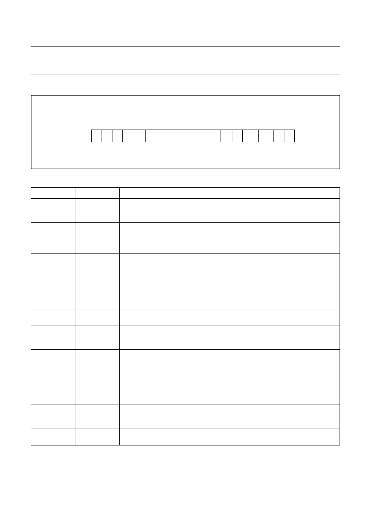
15 14 13 12 11 10 9 8 7 6 5 4 3 2 1 0bit
Fig.18 System Control Register 1 (SYSCON1).
Table 10 Description of SYSCON1 bits.
SYMBOL BIT FUNCTION
− SYSCON1.15
These eight bits are not used.
to
SYSCON1.8
NROD2
NROD1
NROD0
SYSCON1.7
SYSCON1.6
SYSCON1.5
These three bits select the access time for the ROM area. After a reset operation
these bits are logic 0’s. See Table 11.
− SYSCON1.4 not used
− SYSCON1.3 not used
NRAD2
NRAD1
NRAD0
SYSCON1.2
SYSCON1.1
SYSCON1.0
These three bits select the access time for the RAM area. After a reset operation
these bits are logic 0’s. See Table 11
NRAD1NROD2 NROD1 NROD0 NRAD0NRAD2
MLB011
Table 11 Selection of memory access times for ROM and RAM areas.
NROD2 NROD1 NROD0
NRAD2 NRAD1 NRAD0 24 20 16 12
ADD WAIT
STATES
f
XTAL
(MHz)
0 0 0 8 185 235 310 435 ns
0 0 1 4 101 135 185 268 ns
0 1 0 2 60 85 122 185 ns
0 1 1 0 18 35 60 101 ns
Notes
1. 1 internal clock cycle contains 2 wait states.
2. All other states are undefined and reserved.
August 1993 23
UNIT
Philips Semiconductors Product specification
16-bit microcontroller P90CE201
6.3.2 SYSTEM CONTROL REGISTER 2 (SYSCON2)
handbook, full pagewidth
2
I C2
CON
2
I C1
CON
915 14 13 12 11 10bit
T2
PSBPCLK1PSBPCLK
SEL
254 3876
2
TOPSTOED
IM WD
0
I C1
PO
TOED
0
1
1
T1PST1
PO
MLB012
0
Fig.19 System Control Register 2 (SYSCON2).
Table 12 Description of SYSCON2 bits.
SYMBOL BIT FUNCTION
− SYSCON2.15
These three bits are not used.
to
SYSCON2.13
I2C2CON SYSCON2.12 This bit along with the three bits CR0, CR1 and CR2 held in the Serial Control
Register (S2CON), are used to select the bitrate of the I2C-bus 2 interface.
If I2C2CON = 0; the interface operates with a high bitrate. If I2C2CON = 1; the
interface operates with a low bitrate.
2
I
C1CON SYSCON2.11 This bit along with the three bits CR0, CR1 and CR2 held in the Serial Control
Register (S1CON), are used to select the bitrate of the I
2
C-bus 1 interface.
If I2C1CON = 0; the interface operates with a high bitrate. If I2C1CON = 1; the
interface operates with a low bitrate.
T2SEL SYSCON2.10 This bit selects the frequency of the clock for Timer 2. If T2SEL = 0; the timer
operates at a frequency of f
/2. If T2SEL = 1; the timer operates at a frequency
XTAL
of BPCLK/4.
PSBPCLK1
PSBPCLK0
SYSCON2.9
SYSCON2.8
These two bits control the prescaler for the basic peripheral clock. See Table 13.
IM SYSCON2.7 If IM = 0; level 7 is loaded into the Status Register during interrupt processing to
prevent the CPU from being interrupted by another interrupt source. If IM = 1; the
current interrupt level is loaded into the Status Register allowing nested interrupts.
WD SYSCON2.6 This bit enables or disables the Watchdog timer for bus error (internal) detection.
If WD = 0; the timer is disabled. If WD = 1; the timer is enabled for bus error
detection. If no acknowledge has been sent by the addressed device after 128 × 16
internal clock cycles the on-chip bus error signal is activated.
2
I
C1PO SYSCON2.5 The state of this bit determines whether general port pins GP.7/SDA1 and
GP.6/SCL1 are used as port pins or in their I2C-bus function. When I2C1P0 = 0; the
port function is selected. When I2C1P0 = 1; the I2C-bus is selected.
T0PS SYSCON2.4 This bit enables or disables the prescaler for Timer 0. If T0PS = 0; the prescaler is
T0ED1
T0ED0
SYSCON2.3
SYSCON2.2
disabled and the timer operates at a frequency of f
is enabled and the timer operates at a frequency of f
These two bits select which transition at the external input will trigger an increment
of Timer 0. See Table 14.
/2. If T0PS = 1; the prescaler
XTAL
/32.
XTAL
August 1993 24
 Loading...