

Philips p8xce528 DATASHEETS

INTEGRATED CIRCUITS
DATA SH EET
P8xCE528
8-bit microcontroller with EMC and
FEEPROM
Preliminary specification
File under Integrated Circuits, IC20
September 1993

Philips Semiconductors Preliminary specification
8-bit microcontroller with EMC and
FEEPROM
FEATURES
• 80C51 central processing unit
• 32K x 8 ROM resp. FEEPROM, expandable externally
to 64 kbytes
• ROM/FEEPROM code protection
• 512 x 8 RAM, expandable externally to 64 kbytes
• Four 8-bit I/O ports
• Full-duplex UART compatible with the standard 80C51
and the 8052
• Two standard 16-bit timer/counters
• An additional 16-bit timer (functionally equivalent to the
timer 2 of the 8052)
• On-chip Watchdog Timer (WDT) with an on-chip
oscillator
• Bit-level I2C-bus hardware serial I/O Port
• 7-source and 7-vector interrupt structure with 2 priority
levels
• Up to 3 external interrupt request inputs
• Two programmable power reduction modes (Idle and
Power-down)
• Termination of Idle mode by any interrupt, external or
WDT (watchdog) reset
• Wake-up from Power-down by external interrupt,
external or WDT reset
• Software enable/disable of ALE output pulse
• Electro-Magnetic Compatibility (EMC) improvements
• XTAL frequency range: 3.5 MHz to 16 MHz
• 4.5 to 5.5 V supply voltage range
• Extended Temperature range (−40 to +85 °C)
GENERAL DESCRIPTION
The P83CE528; P80CE528; P89CE528 (hereafter
generically referred to as P8xCE528) single-chip 8-bit
microcontroller is manufactured in an advanced CMOS
process and is a derivative of the PCB80C51
microcontroller family.
P8xCE528
This device provides architectural enhancements that
make it applicable in a variety of applications in general
control systems, especially in those systems which need a
large ROM and RAM capacity on chip.
The P8xCE528 contains a non-volatile 32K x 8 read-only
program memory (P83CE528) or FEEPROM (P89CE528),
a volatile 512 x 8 read/write data memory, four 8-bit I/O
ports, two 16-bit timer/event counters (identical to the
timers of the 80C51), a 16-bit timer (identical to the timer 2
of the 8052), a multi-source, two-priority-level, nested
interrupt structure, two serial interfaces (UART and
bit-level I
a watchdog timer (WDT) with a separate on-chip oscillator.
For systems that require extra capability, the P8xCE528
can be expanded using standard TTL compatible
memories and logic.
In addition, the P8xCE528 has two software selectable
modes of power reduction - Idle mode and Power-down
mode. The Idle mode freezes the CPU while allowing the
RAM, timers, serial ports and interrupt system to continue
functioning. The Power-down mode saves the RAM
contents but freezes the oscillator, causing all other chip
functions to be inoperative.
The device also functions as an arithmetic processor
having facilities for both binary and BCD arithmetic plus
bit-handling capabilities. The instruction set consists of
over 100 instructions: 49 one-byte, 45 two-byte and 17
three-byte. With a 16 MHz crystal, 58% of the instructions
are executed in 0.75 µs and 40% in 1.5 µs. Multiply and
divide instructions require 3 µs.
2
C-bus), an on-chip oscillator and timing circuits,
The P8xCE528 has the same instruction set as the 80C51.
Three versions of the derivative exist:
• P83CE528: 32 kbytes mask programmable ROM
• P80CE528: ROMless version of the P83CE528
• P89CE528: 32 kbytes FEEPROM (Flash Electrically
Erasable Program Memory).
September 1993 2
Philips Semiconductors Preliminary specification
8-bit microcontroller with EMC and
FEEPROM
ELECTROMAGNETIC COMPATIBILITY (EMC)
Primary attention is paid to the reduction of
electro-magnetic emission of the microcontroller
P8xCE528. The following features reduce the
electro-magnetic emission and additionally improve the
electromagnetic susceptibility:
• Two supply voltage pins (V
(V
SS1;2;3;4
) are provided on the package as follows:
– one VDD and one VSS as a pair of pins placed
mid-centre on one side of the package
– a second pair of VDD and VSS pins placed mid-centre
on the opposite side of the package
– two more VSS pins, one placed on each of the other
two sides of the package.
• Separated VDD pins for the internal logic and the port
buffers.
• Internal decoupling capacitance improves the EMC
radiation behaviour and the EMC immunity.
• External capacitors are to be located as close as
possible between pins V
and V
; ceramic chip capacitors are recommended
SS3
DD1
(100 nF).
) and four ground pins
DD1;2
and V
as well as V
SS1
DD2
P8xCE528
Recommendation on ALE
For applications that require no external memory or
temporarily no external memory: the ALE output signal
(pulses at a frequency of f
software control (bit 5 in the PCON SFR: `RFI`); if
disabled, no ALE pulse will occur. ALE pin will be pulled
down internally, switching an external address latch to a
quiet state. The MOVX instruction will still toggle ALE as a
normal MOVX. ALE will retain its normal HIGH value
during Idle mode and a LOW value during Power-down
mode while in the `RFI` reduction mode.
Additionally during internal access (EA = 1) ALE will toggle
normally when the address exceeds the internal program
memory size. During external access (EA = 0) ALE will
always toggle normally, whether the flag `RFI` is set or not.
/6) can be disabled under
osc
ORDERING INFORMATION
EXTENDED
TYPE NUMBER
PINS PIN POSITION MATERIAL CODE
PACKAGE
TEMPERATURE
RANGE (°C)
FREQUENCY
(MHz)
ROMless
P80CE528EBB 44 QFP plastic SOT307-2 0 to +70 3.5 to 16
P80CE528EFB 44 QFP plastic SOT307-2 −40 to +85 3.5 to 16
P80CE528EBA 44 PLCC plastic SOT187-2 0 to +70 3.5 to 16
P80CE528EFA 44 PLCC plastic SOT187-2 −40 to +85 3.5 to 16
ROM
P83CE528EBB 44 QFP plastic SOT307-2 0 to +70 3.5 to 16
P83CE528EFB 44 QFP plastic SOT307-2 −40 to +85 3.5 to 16
P83CE528EBA 44 PLCC plastic SOT187-2 0 to +70 3.5 to 16
P83CE528EFA 44 PLCC plastic SOT187-2 −40 to +85 3.5 to 16
FEEPROM
P89CE528EBA 44 PLCC plastic SOT187-2 0 to +70 3.5 to 16
P89CE528EFA 44 PLCC plastic SOT187-2 −40 to +85 3.5 to 16
September 1993 3

Philips Semiconductors Preliminary specification
8-bit microcontroller with EMC and
FEEPROM
RST
T2 T2EX
shared with Port 1
T0 T1
counter inputs
shared with Port 3
TIMER
WATCHDOG
16-BIT
TIMER
TWO 16-BIT
COUNTERS
TIMER/EVENT
2
I C
BIT-LEVEL
INTERFACE
SHIFT
SERIAL PORT
SYNCHRONOUS
PROGRAMMABLE
FULL DUPLEX UART
MLB074
SDA SCL
shared with Port 1
RXD
shared with Port 3
TXD
P8xCE528
reference
frequency
SS
V
DD
V
XTAL2 XTAL1
DATA
(256 x 8
MEMORY
AUX RAM)
DATA
MEMORY
(256 x 8 RAM)
(1)
MEMORY
PROGRAM
FEEPROM)
(32K x 8 ROM/
AND
TIMING
OSCILLATOR
(2)
1K x 8
BOOT ROM
CPU
P83CE528
P80CE528
P89CE528
PROGRAMMABLE I/O
CONTROL
EXPANSION
64 kBYTE BUS
internal
interrupts
and I/O pins
address/data bus
control parallel ports,
(1) not present in P80CE528
(2) only present in P89CE528
INT1
INT0
external interrupts
shared with Port 3
Fig.1 Block diagram.
September 1993 4

Philips Semiconductors Preliminary specification
8-bit microcontroller with EMC and
FEEPROM
XTAL1
XTAL2
EA
PSEN
P8xCE528
V
SS
V
DD
RST
Port 0
address and
data bus
T2
T2EX
RXD / data
TXD / clock
INT0
alternative
functions
(1) Only P89CE528 with alternative function.
INT1
T0
T1
WR
RD
Port 3
ALE
WE
(1)
P8xCE528
Fig.2 Functional diagram.
MLB357
Port 1
Port 2
SCL
SDA
address bus
September 1993 5

Philips Semiconductors Preliminary specification
8-bit microcontroller with EMC and
P8xCE528
FEEPROM
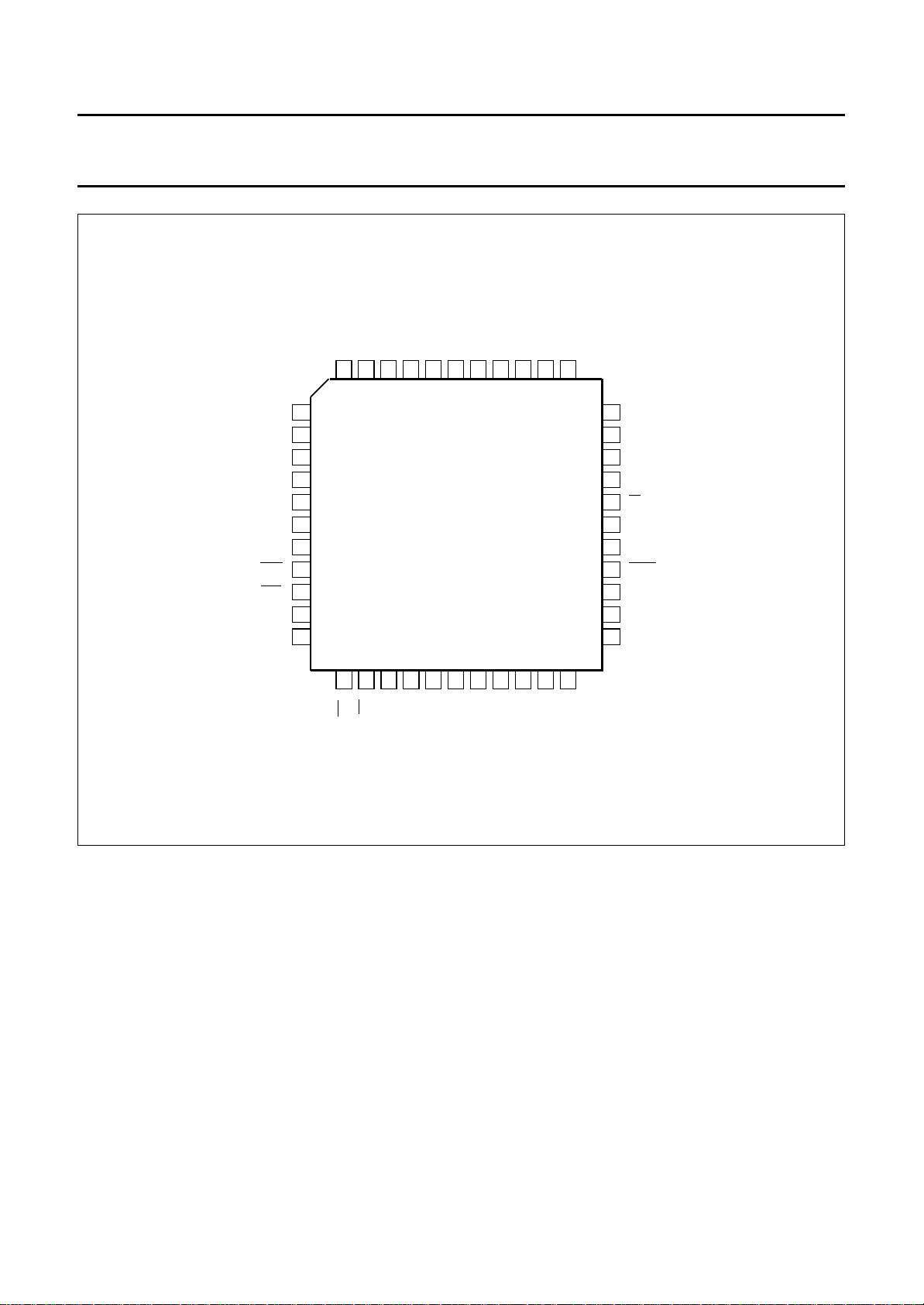
PINNING
Pin description: 44-lead QFP; (SOT307-2).
SYMBOL PIN DESCRIPTION
P1.0 to P1.7 40 to 44
1 to 3
P1.0/T2 40 Timer/event counter 2 external event counter input (falling edge
P1.1/T2EX 41 Timer/event counter 2 capture/reload trigger or external interrupt 2
P1.6/SCL 2 I
P1.7/SDA 3 I
RST 4 RESET: a HIGH level on this pin for two machine cycles while the
P3.0 to P3.7 5, 7 to 13 Port 3: 8-bit quasi-bidirectional I/O Port with internal pull-ups.
Port 1: 8-bit quasi-bidirectional I/O Port. Port 1 can sink/source one
TTL (= 4 LSTTL) input. It can drive CMOS inputs without external
pull-ups, except P1.6 and P1.7 which have open drain outputs.
Port 1 alternative functions:
triggered).
input (falling edge triggered).
2
C-bus Serial Port clock line.
2
C-bus Serial Port data line.
oscillator is running, resets the device. An internal pull-down resistor
permits power-on reset using only a capacitor connected to V
a WDT overflow this pin is pulled HIGH while the internal reset signal is
active.
DD
. After
Port 3 can sink/source one TTL (= 4 LSTTL) input. It can drive CMOS
inputs without external pull-ups.
Port 3 alternative functions:
P3.0/RXD/data 5 Serial Port data input (asynchronous) or data input/output
(synchronous).
P3.1/TXD/clock 7 Serial Port data output (asynchronous) or clock output (synchronous).
INT0 8 External interrupt 0 or gate control input for timer/event counter 0.
P3.2/
INT1 9 External interrupt 1 or gate control input for timer/event counter 1.
P3.3/
P3.4/T0 10 External input for timer/event counter 0.
P3.5/T1 11 External input for timer/event counter 1.
WR 12 External data memory write strobe.
P3.6/
RD 13 External data memory read strobe.
P3.7/
The generation or use of a Port 3 pin as an alternative function is
carried out automatically by the P8xCE528 provided the associated
Special Function Register (SFR) bit is set HIGH.
XTAL2 14 Crystal pin 2: output of the inverting amplifier that forms the oscillator.
This pin left open-circuit when an external oscillator clock is used (see
Figures 15 and 16).
XTAL1 15 Crystal pin 1: input to the inverting amplifier that forms the oscillator,
and input to the internal clock generator. Receives the external
oscillator clock signal when an external oscillator is used (see Figures
15 and 16).
V
SS1;2;3;4
16, 28, 39, 6 Ground: circuit ground potential. All pins must be connected.
September 1993 6

Philips Semiconductors Preliminary specification
8-bit microcontroller with EMC and
P8xCE528
FEEPROM
SYMBOL PIN DESCRIPTION
P2.0 to P2.7 18 to 25 Port 2: 8-bit quasi-bidirectional I/O Port with internal pull-ups. During
access to external memories (RAM/ROM) that use 16-bit addresses
(MOVX @DPTR) Port 2 emits the high-order address byte (A8 to A15).
Port 2 can sink/source one TTL (= 4 LSTTL) input. It can drive CMOS
inputs without external pull-ups.
PSEN 26 Program Store Enable output: read strobe to the external program
memory via Port 0 and Port 2. It is activated twice each machine cycle
during fetches from external program memory. When executing out of
external program memory two activations of PSEN are skipped during
each access to external data memory. PSEN is not activated (remains
HIGH) during no fetches from external program memory. PSEN can
sink/source 8 LSTTL inputs. It can drive CMOS inputs without external
pull-ups.
WE 27 Address Latch Enable output: latches the LOW byte of the address
ALE/
during access to external memory in normal operation. It is activated
every six oscillator periods except during an external data memory
access. ALE/WE can sink/source 8 LSTTL inputs. It can drive CMOS
inputs without an external pull-up (note 1).
EA 29 External Access input: when during RESET, EA is held at a TTL
HIGH level, the CPU executes out of the internal program ROM,
provided the program counter is less than 32768. When EA is held at a
TTL LOW level during RESET, the CPU executes out of external
program memory via Port 0 and Port 2. EA is not allowed to float. EA is
latched during RESET and don't care after RESET.
P0.0 to P0.7 30 to 37 Port 0: 8-bit open drain bidirectional I/O Port. It is also the multiplexed
low-order address and data bus during accesses to external memory
(AD0 to AD7). During these accesses internal pull-ups are activated.
Port 0 can sink/source 8 LSTTL inputs.
V
DD1;2
V
V
DD1
DD2
17 Power supply pin for ports, ALE, PSEN and on-chip oscillator.
38 Power supply pin for internal logic.
Power supply: +5 V power supply pin during normal operation and
power reduction modes. Both pins must be connected.
To avoid a latch-up effect at power-on, the voltage on any pin (at any
time) must not be higher than V
respectively.
+0.5 V or lower than VSS−0.5 V
DD
Note
1. To prohibit the toggling of ALE/WE pin (RFI noise reduction) the bit RFI in the PCON register (PCON.5) must be set
by software. This bit is cleared on RESET and can be cleared by software. When set, ALE/WE pin will be pulled down
internally, switching an external address latch to a quiet state. The MOVX instruction will still toggle ALE/WE as a
normal MOVX. ALE/WE will retain its normal HIGH value during Idle mode and a LOW value during Power-down
mode while in the `RFI` mode. Additionally during internal access (EA = 1) ALE/WE will toggle normally when the
address exceeds the internal program memory size. During external access (EA = 0) ALE/WE will always toggle
normally, whether the flag ‘RFI’ is set or not.
September 1993 7
Philips Semiconductors Preliminary specification
8-bit microcontroller with EMC and
FEEPROM
handbook, full pagewidth
P1.5
P1.6/SCL
P1.7/SDA
RST
P3.0/data/RXD
V
SS4
P3.1/clock/TXD
P3.2/INT0
P3.3/INT1
P3.4/T0
P3.5/T1
1
2
3
4
5
6
7
8
9
10
11
P1.4
44
P1.3
43
P1.2
42
P1.0/T2
P1.1/T2EX
41
40
P83CE528
P80CE528
V
SS3
39
V
38
DD2
P0.1/AD1
P0.0/AD0
37
36
P0.3/AD3
P0.2/AD2
35
34
33
32
31
30
29
28
27
26
25
24
23
P0.4/AD4
P0.5/AD5
P0.6/AD6
P0.7/AD7
EA
V
SS2
ALE
PSEN
P2.7/A15
P2.6/A14
P2.5/A13
P8xCE528
12
13
P3.7/RD
P3.6/WR
14
XTAL2
15
V
XTAL1
16
SS1
17
V
DD1
18
19
P2.0/A8
P2.1/A9
20
21
P2.2/A10
P2.3/A11
22
P2.4/A12
MLB075
Fig.3 Pin configuration: 44-lead QFP; (SOT307-2).
September 1993 8
Philips Semiconductors Preliminary specification
8-bit microcontroller with EMC and
FEEPROM
handbook, full pagewidth
P1.4
P1.3
P1.2
6
5
4
7
P1.5
V
RST
SS4
8
9
10
11
12
13
14
15
16
17
P1.6/SCL
P1.7/SDA
P3.0/data/RXD
P3.1/clock/TXD
P3.2/INT0
P3.3/INT1
P3.4/T0
P3.5/T1
P1.0/T2
P1.1/T2EX
3
2
P83CE528
P80CE528
P89CE528
V
SS3
1
V
44
DD2
P0.0/AD0
P0.1/AD1
43
42
P0.2/AD2
P0.3/AD3
41
40
39
38
37
36
35
34
33
32
31
30
29
P0.4/AD4
P0.5/AD5
P0.6/AD6
P0.7/AD7
EA
V
SS2
ALE/WE
PSEN
P2.7/A15
P2.6/A14
P2.5/A13
P8xCE528
(1)
(1) Only P89CE528 with alternative function.
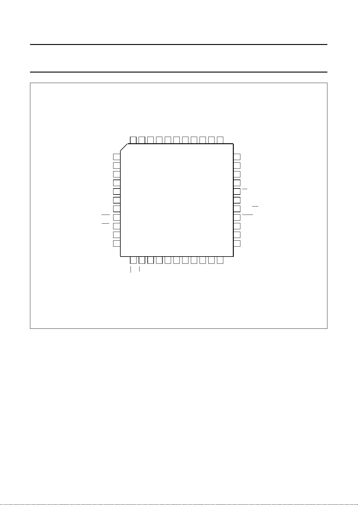
Fig.4 Pin configuration: 44-lead PLCC; (SOT187CG).
18
19
P3.7/RD
P3.6/WR
20
XTAL2
21
V
XTAL1
22
SS1
23
V
DD1
24
25
P2.0/A8
P2.1/A9
26
27
P2.3/A11
P2.2/A10
28
P2.4/A12
MLB076
September 1993 9

Philips Semiconductors Preliminary specification
8-bit microcontroller with EMC and
FEEPROM
FUNCTIONAL DESCRIPTION
General
The P8xCE528 is a stand-alone high-performance
microcontroller designed for use in real time applications
such as instrumentation, industrial control, medium to
high-end consumer applications and specific automotive
control applications.
In addition to the 80C51 standard functions, the device
provides a number of dedicated hardware functions for
these applications. The P8xCE528 is a control-oriented
CPU with on-chip program and data memory. It can be
extended with external program memory up to 64 kbytes.
It can also access up to 64 kbytes of external data
memory. For systems requiring extra capability, the
P8xCE528 can be expanded using standard memories
and peripherals.
The P8xCE528 has two software selectable modes of
reduced activity for further power reduction: Idle and
Power-down. The Idle mode freezes the CPU while
allowing the RAM, timers, serial ports and interrupt system
to continue functioning. The Power-down mode saves the
RAM contents but freezes the oscillator causing all other
chip functions to be inoperative except the WDT if it is
enabled. The Power-down mode can be terminated by an
external reset, a WDT overflow, and in addition, by either
of the two external interrupts.
Memory Organization
The central processing unit (CPU) manipulates operands
in three memory spaces; these are the 64 kbyte external
data memory (of which the lower 256 bytes reside in the
internal AUX-RAM), 512 byte internal data memory
(consisting of 256 bytes standard RAM and 256 bytes
AUX-RAM) and the 64 kbyte internal and external program
memory.
P8xCE528
ROGRAM MEMORY
P
The program memory of the P8xCE528 consists of 32
kbyte of ROM respectively FEEPROM (‘Flash Memory’)
on-chip, externally expandable up to 64 kbyte. If theEA pin
was HIGH during RESET, the P8xCE528 executes out of
the internal program memory unless the address exceeds
7FFFH. Locations 8000H through 0FFFFH are then
fetched from the external program memory. If the EA pin
was LOW during RESET, the P8xCE528 fetches all
instructions from the external program memory. The EA
input level is latched during RESET and is don't care after
RESET. Figure 5 illustrates the program memory address
space.
By setting a mask programmable security bit (ROM)
respectively software programmable security byte
(FEEPROM) the internal memory content is protected i.e.
it cannot be read out by any test mode or by any instruction
in the external program memory space. The MOVC
instructions are the only ones which have access to
program code in the internal or external program memory.
The EA input is latched during RESET and is don't care
after RESET. This implementation prevents reading from
internal program code by switching from external program
memory to internal program memory during MOVC
instruction or an instruction that handles immediate data.
Table 1lists the access to the internal and external
program memory by the MOVC instructions when the
security feature has been activated. If the security feature
is not activated, there are no restrictions for the MOVC
instructions.
September 1993 10

Philips Semiconductors Preliminary specification
8-bit microcontroller with EMC and
FEEPROM
Table 1 Internal and external program memory access with activated security feature
INSTRUCTION
ACCESS TO INTERNAL
PROGRAM MEMORY
MOVC in internal program memory YES YES
MOVC in external program memory NO YES
handbook, full pagewidth
64K
EXTERNAL
ACCESS TO EXTERNAL
PROGRAM MEMORY
64K
P8xCE528
32767
0
32768
INTERNAL
(EA = 1)
PROGRAM MEMORY
EXTERNAL
(EA = 0)
OVERLAPPED SPACE
255
INDIRECT ONLY
127
DIRECT AND
0
INDIRECT
MAIN RAM
INTERNAL DATA MEMORY
SFRs
Fig.5 Memory map and address Space.
AUXILIARY
RAM
MLB077
256
EXTERNAL
DATA MEMORY
September 1993 11

Philips Semiconductors Preliminary specification
8-bit microcontroller with EMC and
FEEPROM
INTERNAL DATA MEMORY
The internal data memory is divided into three physically
separated parts: 256 byte of Main RAM, 256 byte of
AUX-RAM, and a 128 byte special function area (SFR) see
Table 2. These parts can be addressed as follows:
• Main RAM 0 to 127 can be addressed directly and
indirectly as in the 80C51. Address pointers are R0 and
R1 of the selected register bank.
• Main RAM 128 to 255 can only be addressed indirectly.
Address pointers are R0 and R1 of the selected register
bank.
• AUX-RAM 0 to 255 is indirectly addressable in the same
way as the external Data Memory locations 0 to 255 with
the MOVX instructions. Address pointers are R0 and R1
of the selected register bank and DPTR. When
executing from internal program memory, an access to
AUX-RAM 0 to 255 will not affect the Ports P0, P2, P3.6
and P3.7.
• The SFRs can only be addressed directly in the address
range from 128 to 255 (Figure 6 illustrates the SFRs
memory map).
P8xCE528
An access to external Data Memory locations higher than
255 will be performed with the MOVX DPTR instructions in
the same way as in the 80C51 structure, i.e. with P0 and
P2 as data/address bus and P3.6 and P3.7 as write and
read strobe signals. Note that it is impossible to access the
external Data Memory with R0, R1 or DPTR < 256 as
address pointer.
Four 8-bit register banks occupy locations 0 through 31 in
the lower RAM area. Only one of these banks may be
enabled at a time. The next 16 bytes, locations 32 through
47, contain 128 directly addressable bit locations. The
stack can be located anywhere in the internal 256 byte
RAM. The stack depth is only limited by the available
internal RAM space of 256 bytes. All registers except the
Program Counter and the four 8-bit register banks reside
in the SFR address space.
Table 2 Internal data memory access
LOCATION ADDRESSED
Main RAM 0 to 127 DIRECT and INDIRECT
AUX-RAM 0 to 255 INDIRECT only with MOVX
Main RAM 128 to 255 INDIRECT only
SFR 128 to 255 DIRECT only
September 1993 12

Philips Semiconductors Preliminary specification
8-bit microcontroller with EMC and
FEEPROM
Addressing
The P8xCE528 has five modes for addressing:
• Register
• Direct
• Register-Indirect
• Immediate
• Base-Register plus Index-Register-Indirect.
The first three methods can be used for addressing
destination operands. Most instructions have a
`destination/source` field that specifies the data type,
addressing methods and operands involved. For
operations other than MOVs, the destination operand is
also a source operand.
Access to memory addresses is as follows:
• Register in one of the four 8-bit register banks through
Register, Direct or Register-Indirect addressing.
• 512 bytes of internal RAM through Direct or
Register-Indirect addressing. Bytes 0 to 127 of internal
RAM may be addressed directly/indirectly. Bytes 128 to
255 of internal RAM share their address location with the
SFRs and so may only be addressed indirectly as data
RAM. Bytes 0 to 255 of AUX-RAM can only be
addressed indirectly via MOVX.
• SFR through Direct addressing at address locations 128
to 255 (see Figure 6).
• External data memory through Register-Indirect
addressing.
• Program memory look-up tables through Base-Register
plus Index-Register-Indirect addressing.
I/O Facilities
P8xCE528
function of Port 1. Port lines P1.0 and P1.1 may be used
as inputs for Timer 2, P1.1 may also be used as an
additional (third) external interrupt request input. Port lines
P1.6 and P1.7 may be selected as the SCL and SDA lines
of Serial Port SIO1 (I
active while the device is disconnected from VDD, these
pins are provided with open drain drivers. Pins P1.6 and
P1.7 do not have pull-up devices when used as ports.
Ports 0, 1, 2, and 3 perform the following alternative
functions:
• Port 0: provides the multiplexed low-order address and
data bus used for expanding the P8xCE528 with
standard memories and peripherals.
• Port 1: pins can be configured individually to provide:
external interrupt request input (external interrupt 2);
external inputs for Timer/counter 2; SCL and SDA for
the I2C-bus interface.
• Port 2: provides the high-order address bus when
expanding the P8xCE528 with external program
memory and/or external data memory.
• Port 3: pins can be configured individually to provide:
external interrupt request inputs (external interrupt 0/1);
external inputs for Timer/counter 0 and
Timer/counter 1; Serial Port receiver input and
transmitter output; control-signals to read and write
external data memory.
Bits which are not used for the alternative functions may be
used as normal bidirectional I/O pins. The generation or
use of a Port 1 or Port 3 pin as an alternative function is
carried out automatically by the P8xCE528 provided the
associated SFR bit is HIGH. Otherwise the port pin is held
at a logical LOW level.
2
C-bus). Because the I2C-bus may be
The P8xCE528 has four 8-bit ports. Ports 0-3 are the same
as in the 80C51, with the exception of the additional
September 1993 13
Philips Semiconductors Preliminary specification
8-bit microcontroller with EMC and
FEEPROM
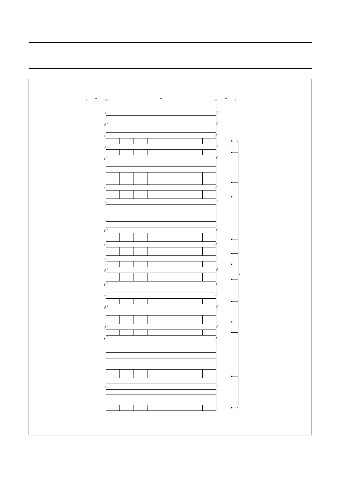
REGISTER
MNEMONIC
(1)
F7 F6 F5 F4 F3 F2 F1 F0 F0HB
E7 E6 E5 E4 E3 E2 E1 E0
SCI/
SDI/
SCO
SDO
DE
DF
CYD7ACD6FOD5RSID4RSOD3OVD2FID1P
BIT MNEMONIC /
BIT ADDRESS (HEX)
CLHDOBBDCRBFDBWBFDASTRD9ENS
DIRECT BYTE
ADDRESS (HEX)
FFHT3
FBHFMCON
E0HACC
DAHS1INT
D9HS1BIT
D8
D8HS1SCS
D0
D0HPSW
CDHTH2
CCHTL2
CBHRCAP2H
CAHRCAP2L
P8xCE528
TL1
PCON
DPH
DPL
SP
TF2CFEXF2CERCLKCDTCLKCCEXEN2CBTR2
- - -BFPS1BEPT2BDPSBCPT1BBPX1BAPT0B9PX0
B7 B6 B5 B4 B3 B2 B1 B0
EAAFES1AEET2ADESACET1ABEX1AAET0A9EX0
SM09FSM19ESM29DREN9CTB89BRB89ATI99RI
97 96 95 94 93 92 91 90
TF18FTR18ETF08DTR08CIE18BIT18AIE089IT0
87 86 85 84 83 82 81 80
(1) Only in P89CE528
CA
C/T2
C9
CP/RL2
C8
B8
A8
98
88
MLB384
C8HT2CON
B8HIP
B0HP3
A8HIE
A5HWDCON
A0HP2 A7 A6 A5 A4 A3 A2 A1 A0
99HSBUF
98HSCON
90HP1
8DHTH1
8CHTH0
8BH
8AHTL0
89HTMOD
88HTCON
87H
83H
82H
81H
80HP0
SFRs containing
directly addressable
bits
September 1993 14
Fig.6 Special Function Registers (SFR) memory map.
Philips Semiconductors Preliminary specification
8-bit microcontroller with EMC and
FEEPROM
strong pull-up
2 oscillator
periods
input data
Q
INPUT
BUFFER
from port latch
read port pin
P8xCE528
+5 V
p2
p1
n
p3
I/O PIN
PORT
1, 2, & 3
MLA759
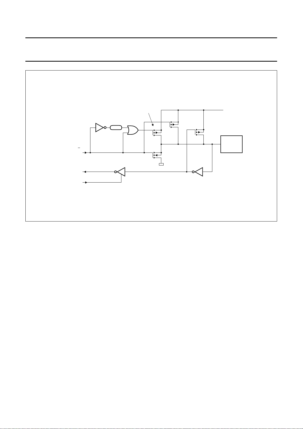
Fig.7 I/O buffers in the P8xCE528 (Ports 1, 2 and 3 except P1.6 and P1.7).
September 1993 15

Philips Semiconductors Preliminary specification
8-bit microcontroller with EMC and
FEEPROM
Timers/Counters
The P8xCE528 contains three 16-bit timer/counters, Timer
0, Timer 1 and Timer 2, and one 8-bit timer, the Watchdog
Timer T3. Timer 0, Timer 1 and Timer 2 may be
programmed to carry out the following functions:
• Measure time intervals and pulse durations
• Count events
• generate interrupt requests.
IMER 0 AND TIMER 1
T
Timers 0 and 1 each have a control bit in TMOD SFR that
selects the timer or counter function of the corresponding
timer. In the timer function, the register is incremented
every machine cycle. Thus, one can think of it as counting
machine cycles. Since a machine cycle consists of 12
oscillator periods, the count rate is 1/12 of the oscillator
frequency.
In the counter function, the register is incremented in
response to a HIGH-to-LOW transition at the
corresponding external input pin, T0 or T1. In this function,
the external input is sampled during S5P2 of every
machine cycle. When the samples show a HIGH in one
cycle and a LOW in the next cycle, the counter is
incremented. Thus, it takes two machine cycles (24
oscillator periods) to recognize a HIGH-to-LOW transition.
There are no restrictions on the duty cycle of the external
input signal, but to ensure that a given level is sampled at
least once before it changes, it should be held for at least
one full machine cycle.
P8xCE528
When Timer 0 is in Mode 3, Timer 1 can be programmed
to operate in Modes 0, 1 or 2 but cannot set an interrupt
request flag and generate an interrupt. However, the
overflow from Timer 1 can be used to pulse the Serial Port
baud-rate generator. With a 16 MHz crystal, the counting
frequency of these timer/counters is as follows:
• In the timer function, the timer is incremented at a
frequency of 1.33 MHz (oscillator frequency divided by
12).
• In the counter function, the frequency handling range for
external inputs is 0 Hz to 0.66 MHz (f
Both internal and external inputs can be gated to the timer
by a second external source for directly measuring pulse
duration.
When configured as a counter, the register is incremented
on every falling edge on the corresponding input pin, T0 or
T1. The incremented register value can be read earliest
during the second machine cycle after that one, in which
the incrementing pulse occurred.
The timers are started and stopped under software control.
Each one sets its interrupt request flag when it overflows
from all logic 1s to all logic 0s (respectively, the automatic
reload value), with the exception of Mode 3 as previously
described.
CLK
/24).
Timer 0 and Timer 1 can be programmed independently to
operate in one of four modes:
• Mode 0: 8-bit timer or 8-bit counter each with
divide-by-32 prescaler
• Mode 1: 16-bit time interval or event counter
• Mode 2: 8-bit time interval or event counter with
automatic reload upon overflow
• Mode 3:
– Timer 0: one 8-bit time interval or event counter and
one 8-bit time interval counter
– Timer 1: stopped.
September 1993 16

Philips Semiconductors Preliminary specification
8-bit microcontroller with EMC and
P8xCE528
FEEPROM
TMOD: TIMER/COUNTER MODE CONTROL REGISTER
This register is located at address 89H.
TMOD SFR (89H).
bit-7 6 5 4 3 2 1 0
GATE C/
Table 3 Description of TMOD bits
MNEMONIC BIT FUNCTION
TIMER 1
GATE TMOD.7 Timer 1 gating control: when set, Timer/counter 1 is enabled only while
T TMOD.6 Timer or counter selector: cleared for timer operation (input from internal system
C/
M1 TMOD.5 Operating mode: see Table 4.
M0 TMOD.4 Operating mode: see Table 4.
TM1M0GATEC/TM1M0
TIMER 1 TIMER 0
INT1 pin is
HIGH and TR1 control bit is set. When cleared, Timer/counter 1 is enabled whenever
TR1 control bit is set.
clock). Set for counter operation (input from T1 input pin).
TIMER 0
GATE TMOD.3 Timer 0 gating control: when set, Timer/counter 0 is enabled only while
HIGH and TR0 control bit is set. When cleared, Timer/counter 0 is enabled whenever
TR0 control bit is set.
T TMOD.2 Timer or counter selector: cleared for timer operation (input from internal system
C/
clock). Set for counter operation (input from T0 input pin).
M1 TMOD.1 Operating mode: see Table 4.
M0 TMOD.0 Operating mode: see Table 4.
Table 4 TMOD M1 and M0 operating modes
M1 M0 FUNCTION
008-bit timer/counter: `THX` with `TLX` as 5-bit prescaler.
0116-bit timer/counter: `THX` and `TLX` are cascaded, there is no prescaler.
108-bit autoload timer/counter: `THX` holds a value which is to be reloaded into
`TLX` each time it overflows.
11Timer 0: TL0 is an 8-bit timer/counter controlled by the standard Timer 0 control
bits. TH0 is an 8-bit timer controlled by Timer 1 control bits.
11Timer 1: Timer/counter 1 stopped.
INT0 pin is
September 1993 17

Philips Semiconductors Preliminary specification
8-bit microcontroller with EMC and
P8xCE528
FEEPROM
TCON: TIMER/COUNTER CONTROL REGISTER
This register is located at address 88H.
TCON SFR (88H).
bit-7 6 543210
TF1 TR1 TF0 TR0 IE1 IT1 IE0 IT0
Table 5 Description of TCON bits
MNEMONIC BIT FUNCTION
TF1 TCON.7 Timer 1 overflow flag: set by hardware on timer/counter overflow. Cleared when
interrupt is processed.
TR1 TCON.6 Timer 1 run control bit: set/cleared by software to turn timer/counter ON/OFF.
TF0 TCON.5 Timer 0 overflow flag: set by hardware on timer/counter overflow. Cleared when
interrupt is processed.
TR0 TCON.4 Timer 0 run control bit: set/cleared by software to turn timer/counter ON/OFF.
IE1 TCON.3 Interrupt 1 edge flag: set by hardware when external interrupt is detected. Cleared
when interrupt is processed.
IT1 TCON.2 Interrupt 1 type control bit: set/cleared by software to specify falling edge/LOW level
triggered external interrupt.
IE0 TCON.1 Interrupt 0 edge flag: set by hardware when external interrupt is detected. Cleared
when interrupt is processed.
IT0 TCON.0 Interrupt 0 type control bit: set/cleared by software to specify falling edge/LOW level
triggered external interrupt.
IMER 2
T
Timer 2 is functionally similar to the Timer 2 of the 8052AH. Timer 2 is a 16-bit timer/counter which is formed by two
SFRs, TL2 and TH2. Another pair of SFRs, RCAP2L and RCAP2H, form a 16-bit capture register or a 16-bit reload
register. Like timers 0 and 1, Timer 2 can operate either as timer or as event counter. This is selected by bit C/T2 in the
T2CON SFR. The timer has three operating modes: capture, autoload and baud rate generator, which are selected by
bits in the T2CON SFR (see Table 6).
Table 6 Timer 2 operating modes
RCLK + TCLK CP/
0 0 1 16-bit automatic reload
0 1 1 16-bit capture
1 X 1 Baud rate generator
X X 0 OFF
RL2 TR2 MODE
September 1993 18

Philips Semiconductors Preliminary specification
8-bit microcontroller with EMC and
P8xCE528
FEEPROM
T2CON: TIMER 2CONTROL REGISTER
This register is located at address C8H.
T2CON SFR (C8H).
bit-7 6 5 4 3 2 1 0
TF2 EXF2 RCLK TCLK EXEN2 TR2 C/
Table 7 Description of T2CON bits
MNEMONIC BIT FUNCTION
TF2 T2CON.7 Timer 2 overflow flag: set by a Timer 2 overflow and must be cleared by software. TF2
will not be set when either RCLK = 1 or TCLK = 1.
EXF2 T2CON.6 Timer 2 external flag: set when either a capture or reload is caused by a negative
transition on T2EX and EXEN2 = 1. When Timer 2 interrupt is enabled, EXF2 = 1 will
cause the CPU to vector to Timer 2 interrupt routine.
RCLK T2CON.5 Receive clock flag: when set, causes the Serial Port to use T imer 2 overflow pulses for
its receive clock in Modes 1 and 3. RCLK = 0 causes Timer 1 overflows to be used for
the receive clock.
TCLK T2CON.4 Transmit clock flag: when set, causes the Serial Port to use Timer 2 overflow pulses
for its transmit clock in Modes 1 and 3. TCLK = 0 causes Timer 1 overflows to be used
for the transmit clock.
EXEN2 T2CON.3 Timer 2 external enable flag: when set, allows a capture or reload to occur as a result
of a negative transition on T2EX if Timer 2 is not being used to clock the Serial Port.
EXEN2 = 0 causes Timer 2 to ignore events at T2EX.
TR2 T2CON.2 Start/stop control: a logic 1 starts Timer 2. A logic 0 stops Timer 2.
T2 T2CON.1 Timer/counter select: 0 = internal timer (OSC/12). 1 = external event counter (falling
C/
edge triggered).
RL2 T2CON.0 Capture/reload flag: when set, capture will occur on negative transitions at T2EX if
CP/
EXEN2 = 1. When cleared, reloads will occur upon either Timer 2 overflows or
negative transitions at T2EX if EXEN2 = 1. When either RCLK = 1 or TCLK = 1, this
bit is ignored and the timer is forced to reload upon overflow.
T2 CP/RL2
September 1993 19
Philips Semiconductors Preliminary specification
8-bit microcontroller with EMC and
FEEPROM
CAPTURE MODE
In the capture mode (see Figure 8) there are two options
which are selected by bit EXEN2 in T2CON. If
EXEN2 = 0, then Timer 2 is a 16-bit timer/counter which
on overflow sets bit TF2 (Timer 2 overflow bit). TF2 can be
used to generate an interrupt. If EXEN2 = 1, Timer 2
operates as above, with the added feature that a
HIGH-to-LOW transition at the external input T2EX causes
the current value in Timer 2 registers (TL2 and TH2) to be
captured into registers RCAP2L and RCAP2H,
respectively. The HIGH-to-LOW transition of T2EX also
causes bit EXF2 in T2CON to be set. EXF2 can be used to
generate an interrupt.
UTOMATIC RELOAD MODE
A
In the automatic reload mode (see Figure 9) there are two
options which are selected by bit EXEN2 in T2CON. If
EXEN2 = 0, then a Timer 2 overflow sets TF2 and causes
the Timer 2 registers to be reloaded with the 16-bit value
in registers RCAP2L and RCAP2H, which are preset by
software.
If EXEN2 = 1, Timer 2 operates as above, with the added
feature that a HIGH-to-LOW transition at the external input
T2EX triggers the 16-bit reload and sets EXF2.
P8xCE528
B
AUD RATE GENERATOR MODE
The baud rate generator mode (see Figure 10) is selected
by RCLK = 1 and/or TCLK = 1 in T2CON. Overflows of
either Timer 2 or Timer 1 can be used independently for
generating baud rates for transmit and receive. The baud
rate generation by Timer 1 and/or Timer 2 is used for the
Serial Port in Mode 1 and Mode 3. The baud rate
generation mode is similar to the automatic reload mode,
in that a rollover in TH2 causes the Timer 2 registers to be
reloaded with the 16-bit value in registers RCAP2L and
RCAP2H, which are preset by software. The baud rate for
the Serial Port in Modes 1 and 3 are determined by Timer
2 overflow rate as follows:
Baud rate
Timer 2 can be configured for either timer or counter
operation. In timer operation a prescaler divides the
oscillator frequency by 2 (by 12 in the previous modes) and
the baud rate is given by the formula:
Baud Rate
In this mode an overflow of Timer 2 does not set TF2. If
EXEN2 = 1, a HIGH-to-LOW transition at pin T2EX sets
EXF2 and can be used to generate an interrupt.
Timer 2 overflow rate
=
------------------------------------------------------- -
=
---------------------------------------------------------------------------------------------------32 65536 RCAP2H, RCAP2L()–[]×
16
oscillator frequency
handbook, full pagewidth
12OSC
T2 PIN
T2EX PIN
C/T2 = 0
C/T2 = 1
transition
detector
control
TR2
control
EXEN2
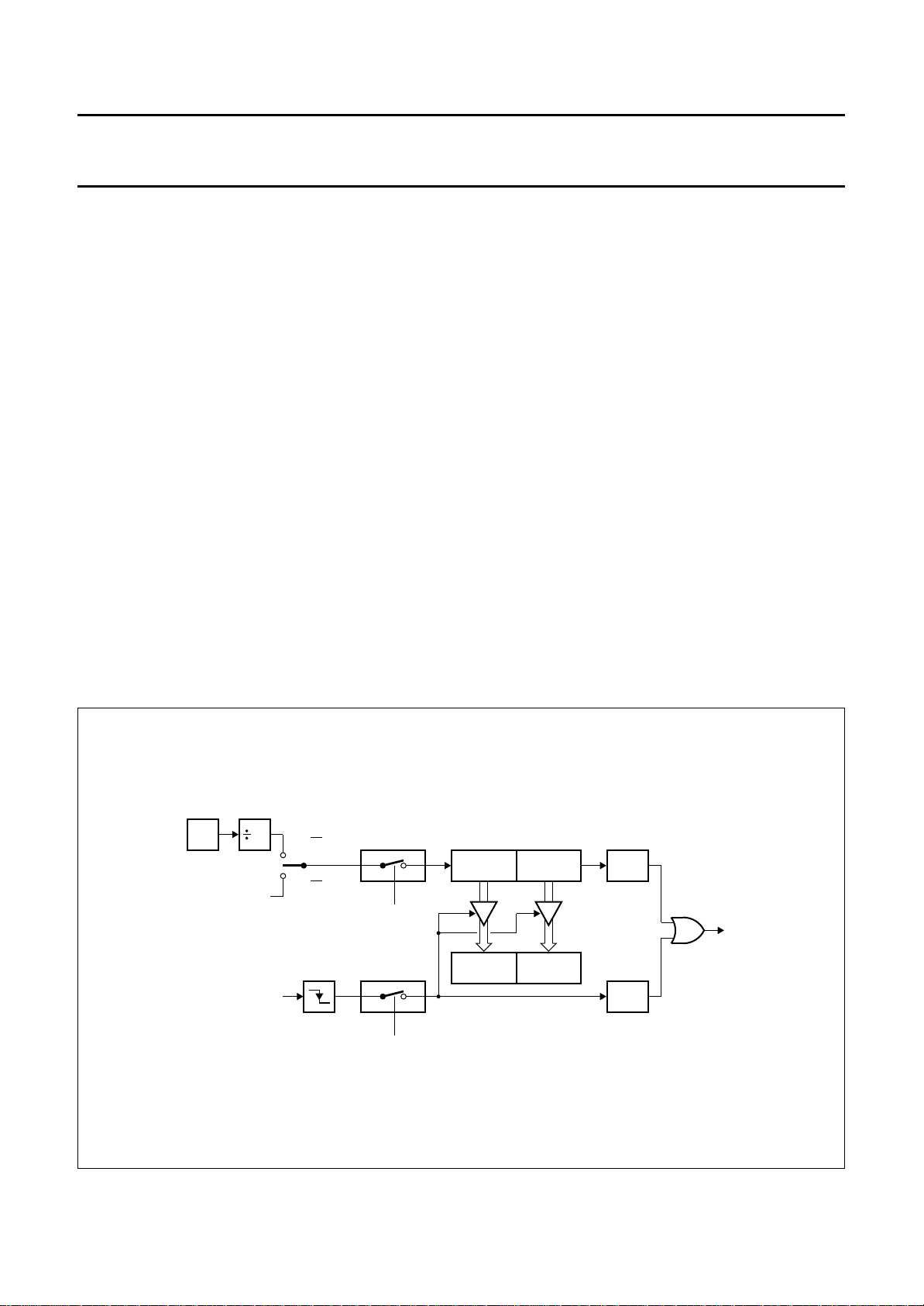
Fig.8 Timer 2 in capture mode.
September 1993 20
TL2
(8 BITS)
RCAP2L RCAP2H
TH2
(8 BITS)
TF2
EXF2
MBC468 - 1
timer 2
interrupt

Philips Semiconductors Preliminary specification
8-bit microcontroller with EMC and
FEEPROM
handbook, full pagewidth
T2EX PIN
T2 PIN
12OSC
C/T2 = 0
C/T2 = 1
transition
detector
TR2
control
EXEN2
control
reload
TL2
(8 BITS)
RCAP2L RCAP2H
TH2
(8 BITS)
TF2
EXF2
P8xCE528
timer 2
interrupt
MBC469 - 1
handbook, full pagewidth
(note: divided by 2
not by 12)
2OSC
T2 PIN
T2EX PIN
C/T2 = 0
C/T2 = 1
transition
detector
Fig.9 Timer 2 in automatic reload mode.
TIMER 1
overflow
10
10
control
TR2
control
EXEN2
TL2
(8 BITS)
RCAP2L RCAP2H
EXF2
TH2
(8 BITS)
"TIMER 2"
interrupt
(additional external
interrupt)
2
10
SMOD
RCLK
16
RX CLOCK
TCLK
TX CLOCK
16
MBC470 - 1
September 1993 21
Fig.10 Timer 2 in baud rate generator mode.

Philips Semiconductors Preliminary specification
8-bit microcontroller with EMC and
FEEPROM
Watchdog Timer T3
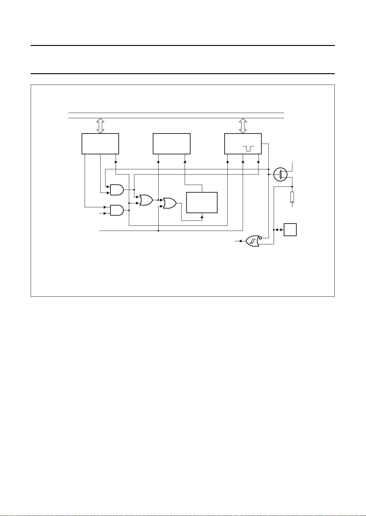
The Watchdog Timer (WDT) see Figure 11, consists of an
11-bit prescaler and an 8-bit timer formed by SFR T3. The
prescaler is incremented by an on-chip oscillator with a
fixed frequency of 1 MHz. The maximum tolerance of this
frequency is −50% and +100%. The 8-bit timer increments
every 2048 cycles of the on-chip oscillator. When a timer
overflow occurs, the microcontroller is reset and a
reset-output-pulse of 16 x 2048 cycles of the on-chip
oscillator is generated at pin RST. The internal RESET
signal is not inhibited when the external RST pin is kept
LOW by e.g. an external reset circuit. The RESET signal
drives Ports 1, 2 and 3 outputs into the HIGH state and
Port 0 into high impedance, no matter if the XTAL-clock is
running or not.
The WDT is controlled by WDCON SFR with the direct
address location A5H. WDCON can be read and written by
software. A value of A5H in WDCON halts the on-chip
oscillator and clears both the prescaler and Timer T3. After
RESET, WDCON contains A5H. Every value other than
A5H in WDCON enables the WDT. When the WDT is
enabled it runs independent of the XTAL-clock.
Timer T3 can be read on the fly. Timer T3 can be written
only if WDCON has previously been loaded with 5AH,
otherwise T3 and the prescaler are not affected. A
successful write operation to T3 also clears the prescaler
and clears WDCON.
P8xCE528
To prevent an overflow of the WDT, the user program has
to reload T3 within periods that are shorter than the
programmed Watchdog time interval. This time interval is
determined by the 8-bit reload value that is written into
register T3.
Watchdog time interval
The advantages of this implementation are:
• Only an internal reset connection to the microcontroller
core.
• The Power-down mode and the Watchdog (WDT)
function can be used concurrently.
• The WDT also monitors the XTAL oscillator. In case of a
failure the port outputs are forced to a defined HIGH
state.
• Interference will not disable the WDT because it is
unlikely that it will force WDCON to A5H.
• Tolerances of the on-chip oscillator can be adjusted by
testing the T3 value and adapting the reload value.
• The WDT can be enabled and disabled under control of
the user software. This gives the possibility to use both
the Watchdog function and the Power-down function.
• The direct address A5H of WDCON and its disable value
A5H will not unintentionally be present at a random
location in the field of program code, except for
immediate data, because the opcode A5H is not used in
the instruction set.
256 T3()–[]2048×
=
------------------------------------------------------------------------on-chip oscillator frequency
September 1993 22
Philips Semiconductors Preliminary specification
8-bit microcontroller with EMC and
FEEPROM
handbook, full pagewidth
WDCON
(1) (1)
WR - T3
RD - T3
(1)
this signal is active if WDCON
contains this hex value
clear input
A5H5AH
clear
11 - BIT
PRESCALER
ON - CHIP -
OSCILLATOR
halt
write
internal
RESET
8 - BIT TIMER
T3
read clear
over-flow
P8xCE528
IBS
V
DD
R
RST
V
SS
RST
MBC471 - 1
Fig.11 Watchdog Timer T3.
Full Duplex Serial Port (UART)
The Serial Port is functionally similar to the implementation in the 8052AH, with the possibility of two different baud rates
for receive and transmit with Timer 1 and Timer 2 as baud rate generators. It is full duplex, meaning it can receive and
transmit simultaneously. It is also receive-buffered, meaning it can commence reception of a second byte before a
previously received byte has been read from the receive register. However, if the first byte still has not been read by the
time the reception of the second byte is complete, one of the bytes will be lost. The Serial Port receive and transmit
registers are both accessed as SBUF SFR. Writing to SBUF loads the transmit register, and reading SBUF accesses the
physically separate receive register.
HE SERIAL PORT OPERATING MODES
T
The Serial Port can operate in one of four modes (see Table 8):
September 1993 23

Philips Semiconductors Preliminary specification
8-bit microcontroller with EMC and
P8xCE528
FEEPROM
Table 8 The Serial Port operating modes
MODE DESCRIPTION
Mode 0 Serial data enters and exits through RXD. TXD outputs the shift clock. 8 bits are transmitted/received:
8 data bits (LSB first). The baud rate is fixed at 1/12 the oscillator frequency.
Mode 1 10 bits are transmitted (through TXD) or received (through RXD): a start bit (0), 8 data bits (LSB first),
and a stop bit (1). On receive, the stop bit is stored in RB8 in SCON SFR. The baud rate is variable.
Mode 2 11 bits are transmitted (through TXD) or received (through RXD): a start bit (0), 8 data bits (LSB first), a
programmable 9th data bit, and a stop bit (1). On transmit, the 9th data bit (TB8 in SCON) usually
represents the parity bit (P, in the PSW). On receive, the 9th data bit is stored in RB8 (SCON), while the
stop bit is ignored. The baud rate is programmable to either 1/32 or 1/64 of the oscillator frequency.
Mode 3 11 bits are transmitted (through TXD) or received (through RXD): a start bit (0), 8 data bits (LSB first), a
programmable 9th data bit, and a stop bit (1). In fact, Mode 3 is the same as Mode 2 in all respects
except the baud rate. The baud rate in Mode 3 is variable.
Note: in all four modes, transmission is initiated by any instruction that uses SBUF as a destination register.
In Mode 0, reception is initiated by the condition RI = 0 and REN = 1.
Reception is initiated by incoming start bit if REN = 1 in the other modes.
September 1993 24
 Loading...