

Philips p80c528, p83c524, p83c528 DATASHEETS

INTEGRATED CIRCUITS
DATA SH EET
P83C524; P80C528; P83C528
8-bit microcontrollers
Product specification
File under Integrated Circuits, IC20
1997 Dec 15

Philips Semiconductors Product specification
8-bit microcontrollers
CONTENTS
1 FEATURES
2 GENERAL DESCRIPTION
3 QUICK REFERENCE DATA
4 ORDERING INFORMATION
5 BLOCK DIAGRAM
6 FUNCTIONAL DIAGRAM
7 PINNING INFORMATION
7.1 Pinning
7.2 Pin description
8 FUNCTIONAL DESCRIPTION
8.1 General
8.2 Instruction Set Execution
9 MEMORY ORGANIZATION
9.1 Program Memory
9.2 Internal Data Memory
9.3 Addressing
10 I/O FACILITIES
11 TIMERS/COUNTERS
11.1 Timer 0 and Timer 1
11.1.1 Timer/Counter Mode Control register (TMOD)
11.1.2 Timer/Counter Control Register (TCON)
11.2 Timer 2
11.2.1 Timer 2 Control Register (T2CON)
11.2.2 Capture Mode
11.2.3 Automatic Reload Mode
11.2.4 Baud Rate Generator Mode
11.3 Watchdog Timer T3
12 SERIAL PORT (UART)
12.1 Serial Port Control Register (SCON)
12.2 SM0 and SM1 operating modes (SCON)
13 BIT-LEVEL I2C INTERFACE
13.1 I2C Interrupt Register (S1INT)
13.2 Single-bit Data Register with I2C Auto-clock
(S1BIT)
13.2.1 Reading or Writing the S1BIT SFR
13.3 Control and Status Register for the I2C-bus
(S1SCS)
14 INTERRUPT SYSTEM
14.1 Interrupt Enable Register (IE)
14.2 Interrupt Priority Register (IP)
14.3 Interrupt Vectors
P83C524; P80C528;
P83C528
15 IDLE AND POWER-DOWN OPERATION
15.1 Power Control Register (PCON)
15.2 Idle Mode
15.3 Power-down Mode
15.4 Wake-up from Power-down Mode
16 OSCILLATOR CIRCUIT
17 RESET CIRCUIT
17.1 Power-on reset
18 INSTRUCTION SET
19 LIMITING VALUES
20 DC CHARACTERISTICS
21 AC CHARACTERISTICS
21.1 AC Characteristics 16 MHz version
21.2 AC Characteristics 24 MHz version
22 I2C CHARACTERISTICS (BIT-LEVEL)
23 XTAL1 CHARACTERISTICS
24 SERIAL PORT CHARACTERISTICS
25 TIMING DIAGRAMS
25.1 Timing symbol definitions
26 PACKAGE OUTLINES
27 SOLDERING
27.1 Introduction
27.2 DIP
27.2.1 Soldering by dipping or by wave
27.2.2 Repairing soldered joints
27.3 PLCC and QFP
27.3.1 Reflow soldering
27.3.2 Wave soldering
27.3.3 Repairing soldered joints
28 DEFINITIONS
29 LIFE SUPPORT APPLICATIONS
30 PURCHASE OF PHILIPS I2C COMPONENTS
1997 Dec 15 2

Philips Semiconductors Product specification
8-bit microcontrollers P83C524; P80C528; P83C528
1 FEATURES
• 80C51 CPU
• 32 kbytes on-chip ROM, expandable externally to
64 kbytes Program Memory address space
• P83C524:
– 16 kbytes on-chip ROM, expandable externally from
32 kbytes to 64 kbytes Program Memory address
space (address space 16 k to 32 k not usable)
• P80C528:
– ROMless version of P83C528
• P83C528:
– 32 kbytes on-chip ROM, expandable externally from
32 kbytes to 64 kbytes Program Memory address
space
• EPROM versions are available: see separate data sheet
P87C524 and P87C528
• 512 bytes on-chip RAM, expandable externally to
64 kbytes Data Memory address space
• Four 8-bit I/O ports
• Full-duplex UART compatible with the standard 80C51
and the 8052
• Two standard 16-bit timer/counters
• An additional 16-bit timer (functionally equivalent to the
timer 2 of the 8052)
• On-chip Watchdog Timer (WDT) with an own oscillator
• Bit-level I2C-bus hardware serial I/O Port
• 7-source and 7-vector interrupt structure with 2 priority
levels
• Up to 3 external interrupt request inputs
• Two programmable power reduction modes (Idle and
Power-down)
• Termination of Idle mode by any interrupt, external or
WDT (watchdog) reset
• Wake-up from Power-down by external interrupt,
external or WDT reset
• ROM code protection
• XTAL frequency range: 3.5 MHz to 16 MHz and
3.5 MHz to 24 MHz
• All packaging pin-outs fully compatible to the standard
8051/8052.
2 GENERAL DESCRIPTION
The P83C524 and P83C528 single-chip 8-bit
microcontrollers are manufactured in an advanced CMOS
process and are derivatives of the PCB80C51
microcontroller family. These devices provide architectural
enhancements that make them applicable in a variety of
applications in general control systems, especially in those
systems which need a large ROM and RAM capacity on
chip.
The P83C524 and P83C528 contain a non-volatile
16 k × 8 respectively 32 k × 8 read-only program memory,
a volatile 512 bytes × 8 read/write data memory, four 8-bit
I/O ports, two 16-bit timer/event counters (identical to the
timers of the 80C51), a 16-bit timer (identical to the timer 2
of the 8052), a multi-source, two-priority-level, nested
interrupt structure, two serial interfaces (UART and
bit-level I2C-bus), a watchdog timer (WDT) with a separate
oscillator, an on-chip oscillator and timing circuits. For
systems that require extra capability, the P83C524 and
P83C528 can be expanded using standard TTL
compatible memories and logic.
The device also functions as an arithmetic processor
having facilities for both binary and BCD arithmetic plus
bit-handling capabilities. The P83C524 and P83C528
have the same instruction set as the PCB80C51 which
consists of over 100 instructions: 49 one-byte, 46 two-byte
and 16 three-byte. With a 16 MHz crystal, 58% of the
instructions are executed in 750 ns and 40% in 1.5 µs.
Multiply and divide instructions require 3 µs.
1997 Dec 15 3
Philips Semiconductors Product specification
8-bit microcontrollers P83C524; P80C528; P83C528
3 QUICK REFERENCE DATA
SYMBOL PARAMETER CONDITION MIN. MAX. UNIT
P83C524, P80C528, P83C528 (see characteristics tables for extended temperature range versions)
V
DD
I
DD
I
ID
I
PD
P
tot
T
stg
T
amb
4 ORDERING INFORMATION
supply voltage range 4.5 5.5 V
supply current: operating modes 16 MHz VDD= 5.5 V, f
supply current: Idle mode 16 MHz VDD= 5.5 V, f
= 16 MHz − 33 mA
CLK
= 16 MHz − 6mA
CLK
supply current: Power-down mode 2V ≤ VPD≤ VDD max. − 100 µA
total power dissipation − 1W
storage temperature range −65 +150 °C
operating ambient temperature range −40 +85 °C
EXTENDED
TYPE NUMBER
NAME DESCRIPTION VERSION
PACKAGE
TEMPERATURE
RANGE (°C)
FREQ.
(MHZ)
ROMless
P80C528EBP DIP40 plastic dual in-line package;
P80C528EFP −40 to +85
40 leads (600 mil)
SOT129-1 0 to +70 3.5 to 16
P80C528IBP 0 to +70 3.5 to 24
P80C528IFP −40 to +85
P80C528EBA PLCC44 plastic leaded chip carrier; 44 leads SOT187-2 0 to +70 3.5 to 16
P80C528EFA −40 to +85
P80C528IBA 0 to +70 3.5 to 24
P80C528IFA −40 to +85
P80C528EBB QFP44 plastic quad flat package;
P80C528EFB −40 to +85
P80C528IBB 0 to +70 3.5 to 24
44 leads (lead length 1.3 mm);
body 10 × 10 × 1.75 mm
SOT307-2 0 to +70 3.5 to 16
P80C528IFB −40 to +85
ROM
P83C524EBP DIP40 plastic dual in-line package;
P83C524EFP −40 to +85
40 leads (600 mil)
SOT129-1 0 to +70 3.5 to 16
P83C524IBP 0 to +70 3.5 to 24
P83C524IFP −40 to +85
P83C524EBA PLCC44 plastic leaded chip carrier; 44 leads SOT187-2 0 to +70 3.5 to 16
P83C524EFA −40 to +85
P83C524IBA 0 to +70 3.5 to 24
P83C524IFA −40 to +85
P83C524EBB QFP44 plastic quad flat package;
P83C524EFB −40 to +85
P83C524IBB 0 to +70 3.5 to 24
44 leads (lead length 1.3 mm);
body 10 × 10 × 1.75 mm
SOT307-2 0 to +70 3.5 to 16
P83C524IFB −40 to +85
1997 Dec 15 4
Philips Semiconductors Product specification
8-bit microcontrollers P83C524; P80C528; P83C528
EXTENDED
TYPE NUMBER
P83C528EBP DIP40 plastic dual in-line package;
P83C528EFP −40 to +85
P83C528IBP 0 to +70 3.5 to 24
P83C528IFP −40 to +85
P83C528EBA PLCC44 plastic leaded chip carrier; 44 leads SOT187-2 0 to +70 3.5 to 16
P83C528EFA −40 to +85
P83C528IBA 0 to +70 3.5 to 24
P83C528IFA −40 to +85
P83C528EBB QFP44 plastic quad flat package;
P83C528EFB −40 to +85
P83C528IBB 0 to +70 3.5 to 24
P83C528IFB −40 to +85
NAME DESCRIPTION VERSION
40 leads (600 mil)
44 leads (lead length 1.3 mm);
body 10 × 10 × 1.75 mm
PACKAGE
TEMPERATURE
RANGE (°C)
SOT129-1 0 to +70 3.5 to 16
SOT307-2 0 to +70 3.5 to 16
FREQ.
(MHZ)
1997 Dec 15 5

This text is here in white to force landscape pages to be rotated correctly when browsing through the pdf in the Acrobat reader.This text is here in
_white to force landscape pages to be rotated correctly when browsing through the pdf in the Acrobat reader.This text is here inThis text is here in
white to force landscape pages to be rotated correctly when browsing through the pdf in the Acrobat reader. white to force landscape pages to be ...
1997 Dec 15 6
frequency
reference
counters
5 BLOCK DIAGRAM
8-bit microcontrollers P83C524; P80C528; P83C528
Philips Semiconductors Product specification
XTAL2 XTAL1
OSCILLATOR
AND
TIMING
CPU
internal
interrupts
INT1
INT0
external interrupts
RAM
PROGRAM
PROGRAM
MEMORY
MEMORY
(32 Kx 8 ROM
(32 K x 8 ROM/
or 16 K x 8 ROM)
EPROM)
64K-BYTE BUS
EXPANSION
CONTROL
control parallel ports,
DATA
MEMORY
(256 x 8 RAM)
PROGRAMMABLE I/O
address/data bus
and I/O pins
AUX - RAM
DATA
MEMORY
(256 x 8 RAM)
P83C524
P80C528
P83C528
T0 T1
TWO 16-BIT
TIMER/EVENT
COUNTERS
PROGRAMMABLE
SERIAL PORT
FULL DUPLEX UART
SYNCHRONOUS
SHIFT
serial in
shared with Port 3
serial out
T2 T2EX
16-BIT
TIMER
BIT-LEVEL
2
I C
INTERFACE
SDA SCL
RST
WATCHDOG
TIMER
MBC455
Fig.1 Block diagram.
handbook, full pagewidth
Philips Semiconductors Product specification
8-bit microcontrollers P83C524; P80C528; P83C528
6 FUNCTIONAL DIAGRAM
handbook, full pagewidth
alternative
functions
RXD / data
TXD / clock
INT0
INT1
WR
RD
T0
T1
XTAL1
XTAL2
PSEN
Port 3
EA
ALE
V
SS
V
DD
P83C524
P80C528
P83C528
P83C528
RST
Port 0
Port 1
Port 2
address and
data bus
T2
T2EX
SCL
SDA
address bus
Fig.2 Functional diagram.
1997 Dec 15 7
MBC454 - 1

Philips Semiconductors Product specification
8-bit microcontrollers P83C524; P80C528; P83C528
7 PINNING INFORMATION
7.1 Pinning
handbook, halfpage
T2EX P1.1
RXD / data P3.0
TXD / clock P3.1
T2 P1.0
P1.2
P1.3
P1.4
P1.5
SCL P1.6
SDA P1.7
RST
INT0 P3.2
INT1 P3.3
T0 P3.4
T1 P3.5
WR P3.6
RD P3.7
1
2
3
4
5
6
7
8
9
10
11
12
13
15
16
17
P83C524
P80C528
P83C528
P83C528
40
39
38
37
36
35
34
33
32
31
30
29
28
2714
26
25
24
V
DD
P0.0 AD0
P0.1 AD1
P0.2 AD2
P0.3 AD3
P0.4 AD4
P0.5 AD5
P0.6 AD6
P0.7 AD7
EA
ALE
PSEN
P2.7 A15
P2.6 A14
P2.5 A13
P2.4 A12
P2.3 A11
18
XTAL2
19
XTAL1
20
V
SS
Fig.3 Pin configuration DIP40 (SOT129-1).
1997 Dec 15 8
MBC453
23
22
21
P2.2 A10
P2.1 A9
P2.0 A8

Philips Semiconductors Product specification
8-bit microcontrollers P83C524; P80C528; P83C528
DD
V
P1.0 / T2
n.c.
P0.0 / AD0
P0.1 / AD1
P0.2 / AD2
42
41
36
35
26
27
21
20
P2.3 / A11
P2.2 / A10
P0.3 / AD3
40
34
39
38
33
37
32
36
31
35
30
34
29
33
28
32
27
31
26
30
25
29
24
23
MBC452
28
22
P2.4 / A12
P0.4 / AD4
P0.5 / AD5
P0.6 / AD6
P0.7 / AD7
EA
n.c.
ALE
PSEN
P2.7 / A15
P2.6 / A14
P2.5 / A13
handbook, full pagewidth
P1.5
SCL / P1.6
SDA / P1.7
RST
RXD / data / P3.0
n.c.
TXD / clock / P3.1
INT0 / P3.2
INT1 / P3.3
T0 / P3.4
T1 / P3.5
P1.3
P1.2
5
4
42
43
19
20
13
14
XTAL2
RD / P3.7
P1.1 / T2EX
1
3
2
39
41
40
P83C524
P80C528
P83C528
P83C528
21
22
23
SS
n.c.
16
15
17
V
XTAL1
44
43
37
38
24
25
18
19
P2.0 / A8
P2.1 / A9
P1.4
6
7
8
1
9
2
10
3
11
4
12
5
13
6
14
7
15
8
16
9
17
10
11
44
18
12
WR / P3.6
Fig.4 Pin configuration QFP44 (SOT307-2).
1997 Dec 15 9

Philips Semiconductors Product specification
8-bit microcontrollers P83C524; P80C528; P83C528
DD
V
P1.0 / T2
n.c.
P0.0 / AD0
P0.1 / AD1
P0.2 / AD2
handbook, full pagewidth
P1.4
6
P1.3
5
P1.1 / T2EX
P1.2
4
3
1
2
44
43
P0.3 / AD3
42
41
40
P1.5
SCL / P1.6
SDA / P1.7
RST
RXD / data / P3.0
n.c.
TXD / clock / P3.1
INT0 / P3.2
INT1 / P3.3
T0 / P3.4
T1 / P3.5
7
8
9
10
11
12
13
14
15
16
17
18
19
RD / P3.7
WR / P3.6
20
XTAL2
P83C524
P80C528
P83C528
P83C528
21
22
SS
V
XTAL1
23
n.c.
24
25
P2.0 / A8
P2.1 / A9
26
27
P2.3 / A11
P2.2 / A10
39
38
37
36
35
34
33
32
31
30
29
MBC452
28
P2.4 / A12
P0.4 / AD4
P0.5 / AD5
P0.6 / AD6
P0.7 / AD7
EA
n.c.
ALE
PSEN
P2.7 / A15
P2.6 / A14
P2.5 / A13
Fig.5 Pin configuration PLCC44 (SOT187-2).
1997 Dec 15 10
Philips Semiconductors Product specification
8-bit microcontrollers P83C524; P80C528; P83C528
7.2 Pin description Table 1 Pin description for P83C524, P80C528 and P83C528; see note 1
SYMBOL
DESCRIPTION
SOT 129-1 SOT 187-2 SOT 307-2
PIN
P1.0−P1.7 1 to 8 2−9
(1 n.c.)
1−3,
40−44
(39 n.c.)
Port 1: 8-bit quasi-bidirectional I/O Port. Port 1 can sink/source
one TTL (= 4 LSTTL) input. It can drive CMOS inputs without
external pull-ups, except P1.6 and P1.7 which have open drain
outputs.
Port 1 alternative functions:
T21240P1.0 Timer/event counter 2 external event counter input
(falling edge triggered)
T2EX 2 3 41 P1.1 Timer/event counter 2 capture/reload trigger or external
interrupt 2 input (falling edge triggered)
SCL 7 8 2 P1.6 I
SDA 8 9 3 P1.7 I
2
C-bus Serial Port clock line
2
C-bus Serial Port data line.
RST 9 10 4 RESET: a HIGH level on this pin for two machine cycles while the
oscillator is running, resets the device. An internal pull-down
resistor permits power-on reset using only a capacitor connected
. After a WDT overflow this pin is pulled HIGH while the
to V
DD
internal reset signal is active.
P3.0−P3.7 10−17 11, 13−19
(12 n.c.)
5, 7−13
(6 n.c.)
Port 3: 8-bit quasi-bidirectional I/O Port with internal pull-ups.
Port 3 can sink/source one TTL (= 4 LSTTL) input. It can drive
CMOS inputs without external pull-ups.
Port 3 alternative functions:
RXD/data 10 11 5 P3.0 Serial Port data input (asynchronous) or data
input/output (synchronous)
TXD/clock 11 13 7 P3.1 Serial Port data output (asynchronous) or clock output
(synchronous)
INT0 12 14 8 P3.2 external interrupt 0 or gate control input for timer/event
counter 0
INT1 13 15 9 P3.3 external interrupt 1 or gate control input for timer/event
counter 1
T0 14 16 10 P3.4 external input for timer/event counter 0
T1 15 17 11 P3.5 external input for timer/event counter 1
WR 16 18 12 P3.6 external data memory write strobe
RD 17 19 13 P3.7 external data memory read strobe.
The generation or use of a Port 3 pin as an alternative function is
carried out automatically by the P83C528 provided the associated
Special Function Register (SFR) bit is set HIGH.
XTAL2 18 20 14 Crystal input 2: output of the inverting amplifier that forms the
oscillator. This pin left open-circuit when an external oscillator
clock is used (see Figures 22 and 23).
1997 Dec 15 11

Philips Semiconductors Product specification
8-bit microcontrollers P83C524; P80C528; P83C528
SYMBOL
DESCRIPTION
SOT 129-1 SOT 187-2 SOT 307-2
XTAL1 19 21 15 Crystal input 1: input to the inverting amplifier that forms the
oscillator, and input to the internal clock generator. Receives the
external oscillator clock signal when an external oscillator is used
(see Figures 22 and 23).
PIN
V
SS
P2.0-P2.7 21−28 24−31
20 22 16 Ground: circuit ground potential.
(23 n.c.)
18−25
(17 n.c.)
Port 2: 8-bit quasi-bidirectional I/O Port with internal pull-ups.
During access to external memories (RAM/ROM) that use 16-bit
addresses (MOVX @DPTR) Port 2 emits the high-order address
byte (A8 to A15). Port 2 can sink/source one TTL (= 4 LSTTL)
input. It can drive CMOS inputs without external pull-ups.
PSEN 29 32 26 Program Store Enable output: read strobe to the external
program memory via Port 0 and Port 2. It is activated twice each
machine cycle during fetches from external program memory.
When executing out of external program memory two activations of
PSEN are skipped during each access to external data memory.
PSEN is not activated (remains HIGH) during no fetches from
external program memory .PSEN can sink/source 8 LSTTL inputs.
It can drive CMOS inputs without external pull-ups.
ALE 30 33 27 Address Latch Enable output: latches the LOW byte of the
address during access to external memory in normal operation. It
is activated every six oscillator periods except during an external
data memory access. ALE can sink/source 8 LSTTL inputs. It can
drive CMOS inputs without an external pull-up.
EA 31 35
(34 n.c.)29(28 n.c.)
External Access input: when during RESET, EA is held at a TTL
HIGH level, the CPU executes out of the internal program ROM,
provided the program counter is less than 32768. When EA is held
at a TTL LOW level during RESET, the CPU executes out of
external program memory via Port 0 and Port 2. EA is not allowed
to float.
P0.0-P0.7 32−39 36−43 30−37 Port 0: 8-bit open drain bidirectional I/O Port. It is also the
multiplexed low-order address and data bus during accesses to
external memory (AD0 to AD7). During these accesses internal
pull-ups are activated. Port 0 can sink/source 8 LSTTL inputs.
V
DD
40 44 38 Power supply: +5 V power supply pin during normal operation,
Idle mode and Power-down mode.
Note
1. To avoid a 'latch-up' effect at power-on, the voltage on any pin (at any time) must not be higher than VDD+0.5 V or
lower than VSS−0.5 V respectively.
1997 Dec 15 12

Philips Semiconductors Product specification
8-bit microcontrollers P83C524; P80C528; P83C528
8 FUNCTIONAL DESCRIPTION
8.1 General
The P83C524, P80C528 and P83C528 are stand-alone
high-performance microcontrollers designed for use in real
time applications such as instrumentation, industrial
control, medium to high-end consumer applications and
specific automotive control applications.
In addition to the 80C51 standard functions, the devices
provide a number of dedicated hardware functions for
these applications. The P83C524 and P83C528 are
control-oriented CPUs with on-chip program and data
memory. They can be extended with external program
memory up to 64 kbytes. They can also access up to
64 kbytes of external data memory. For systems requiring
extra capability, the P83C524 and P83C528 can be
expanded using standard memories and peripherals.
The P83C524, P80C528 and P83C528 have two software
selectable modes of reduced activity for further power
reduction: Idle and Power-down. The Idle mode freezes
the CPU while allowing the RAM, timers, serial ports and
interrupt system to continue functioning. The Power-down
mode saves the RAM contents but freezes the oscillator
causing all other chip functions to be inoperative except
the WDT if it is enabled. The Power-down mode can be
terminated by an external reset, a WDT overflow, and in
addition, by either of the two external interrupts.
9.1 Program Memory
The program memory address space of the P83C528
comprises an internal and an external memory portion.
The P83C528 has 32 kbyte of program memory on-chip.
The program memory can be externally expanded up to 64
kbyte. If the EA pin is held HIGH, the P83C528 executes
out of the internal program memory unless the address
exceeds 7FFFH. Locations 8000H through 0FFFFH are
then fetched from the external program memory. If the EA
pin is held LOW, the P83C528 fetches all instructions from
the external program memory. Fig.6 illustrates the
program memory address space.
By setting a mask programmable security bit the ROM
content is protected i.e. it cannot be read out by any test
mode or by any instruction in the external program
memory space. The MOVC instructions are the only ones
which have access to program code in the internal or
external program memory. The EA input is latched during
RESET and is 'don't care' after RESET. This
implementation prevents reading from internal program
code by switching from external program memory to
internal program memory during MOVC instruction or an
instruction that handles immediate data. Table 2 lists the
access to the internal and external program memory by the
MOVC instructions when the security bit has been set to a
logical one. If the security bit has been set to a logical 0
there are no restrictions for the MOVC instructions.
8.2 Instruction Set Execution
The P83C524, P80C528 and P83C528 use the powerful
instruction set of the 80C51. Additional SFRs are
incorporated to control the on-chip peripherals. The
instruction set consists of 49 single-byte, 46 two-byte and
16 three-byte instructions. When using a 16 MHz
oscillator, 64 instructions execute in 750 ns and 45
instructions execute in 1.5 s. Multiply and divide
instructions execute in 3 µs (see Chapter 18).
9 MEMORY ORGANIZATION
The central processing unit (CPU) manipulates operands
in three memory spaces; these are the 64 kbyte external
data memory (of which the lower 256 bytes reside in the
internal AUX-RAM), 512 byte internal data memory
(consisting of 256 bytes standard RAM and 256 bytes
AUX-RAM) and the 64 kbyte internal and external program
memory.
handbook, halfpage
32767
(1)
16383
00
(1) Only for P83C524.
64 K
32768
INTERNAL
(EA = 1)
(EA = 1)
PROGRAM MEMORY
EXTERNAL
32767
Fig.6 Program Memory Address Space.
EXTERNAL
(EA = 0)
(EA = 0)
MBC456 - 1
1997 Dec 15 13
Philips Semiconductors Product specification
8-bit microcontrollers P83C524; P80C528; P83C528
Table 2 Internal and external program memory access with security bit set
INSTRUCTION
MOVC in internal program memory YES YES
MOVC in external program memory NO YES
9.2 Internal Data Memory
The internal data memory is divided into three physically
separated parts: 256 byte of RAM, 256 byte of AUX-RAM,
and a 128 byte special function area (SFR). These parts
can be addressed as follows (see Table 3 and Fig.11):
• RAM 0 to 127 can be addressed directly and indirectly
as in the 80C51. Address pointers are R0 and R1 of the
selected register bank.
• RAM 128 to 255 can only be addressed indirectly.
Address pointers are R0 and R1 of the selected register
bank.
• AUX-RAM 0 to 255 is indirectly addressable as the
external data memory locations 0 to 255 with the MOVX
instructions. Address pointers are R0 and R1 of the
selected register bank and DPTR. When executing from
internal program memory, an access to AUX-RAM 0 to
255 will not affect the ports P0, P2, P3.6 and P3.7.
• the SFRs can only be addressed directly in the address
range from 128 to 255.
ACCESS TO INTERNAL
PROGRAM MEMORY
An access to external data memory locations higher than
255 will be performed with the MOVX DPTR instructions in
the same way as in the 80C51 structure, i.e. with P0 and
P2 as data/address bus and P3.6 and P3.7 as write and
read timing signals (see Figures 7, 8, 9 and 10). Note that
the external data memory cannot be accessed with R0 and
R1 as address pointer.
Fig.11 shows the internal and external data memory
address space. Fig.12 shows the Special Function
Register (SFR) memory map. Four 8-bit register banks
occupy locations 0 through 31 in the lower RAM area. Only
one of these banks may be enabled at a time. The next 16
bytes, locations 32 through 47, contain 128 directly
addressable bit locations.
The stack can be located anywhere in the internal 256 byte
RAM. The stack depth is only limited by the available
internal RAM space of 256 bytes. All registers except the
Program Counter and the four 8-bit register banks reside
in the SFR address space.
ACCESS TO EXTERNAL
PROGRAM MEMORY
Table 3 Internal data memory access
LOCATION ADDRESSED
RAM 0 to 127 DIRECT and INDIRECT
RAM 128 to 255 INDIRECT only
AUX-RAM 0 to 255 INDIRECT only with MOVX
Special Function Register (SFR) 128 to 255 DIRECT only
1997 Dec 15 14
Philips Semiconductors Product specification
8-bit microcontrollers P83C524; P80C528; P83C528
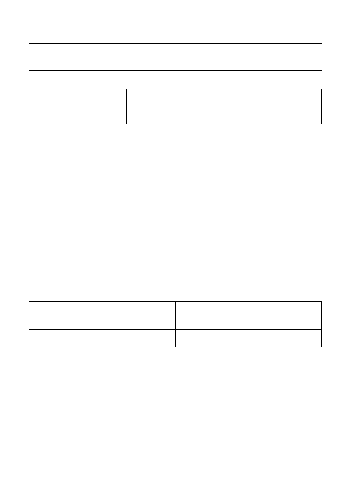
handbook, full pagewidth
S1 S2 S3 S4 S5 S6 S1 S2 S3 S4 S5 S6
ALE
PSEN
RD
WR
P2 P2 OUT
P0 P0 OUT
one machine cycle
a. Without a MOVX.
handbook, full pagewidth
S1 S2 S3 S4 S5 S6 S1 S2 S3 S4 S5 S6
cycle 1 cycle 2
one machine cycle
MBC457
ALE
PSEN
RD
WR
P2 P2 OUT
P0 P0 OUT
b. With a MOVX to the AUX-RAM (read and write).
Fig.7 Internal program memory execution.
1997 Dec 15 15
MBC458
Philips Semiconductors Product specification
8-bit microcontrollers P83C524; P80C528; P83C528
handbook, full pagewidth
ALE
PSEN
RD
WR
P2
P0
handbook, full pagewidth
cycle 1 cycle 2
S1 S2 S3 S4 S5 S6 S1 S2 S3 S4 S5 S6
P2 OUT DPH OUT
P0 OUT
DPL
OUT
DATA
IN
P2 OUT
MBC459
a. With a MOVX to the External Data Memory (read).
cycle 1 cycle 2
S1 S2 S3 S4 S5 S6 S1 S2 S3 S4 S5 S6
ALE
PSEN
RD
WR
P2
P0
P2 OUT DPH OUT
P0 OUT
DPL
OUT
DATA OUT
b. With a MOVX to the External Data Memory (write).
Fig.8 Internal program memory execution (continued).
P2 OUT
MBC460
1997 Dec 15 16

Philips Semiconductors Product specification
8-bit microcontrollers P83C524; P80C528; P83C528
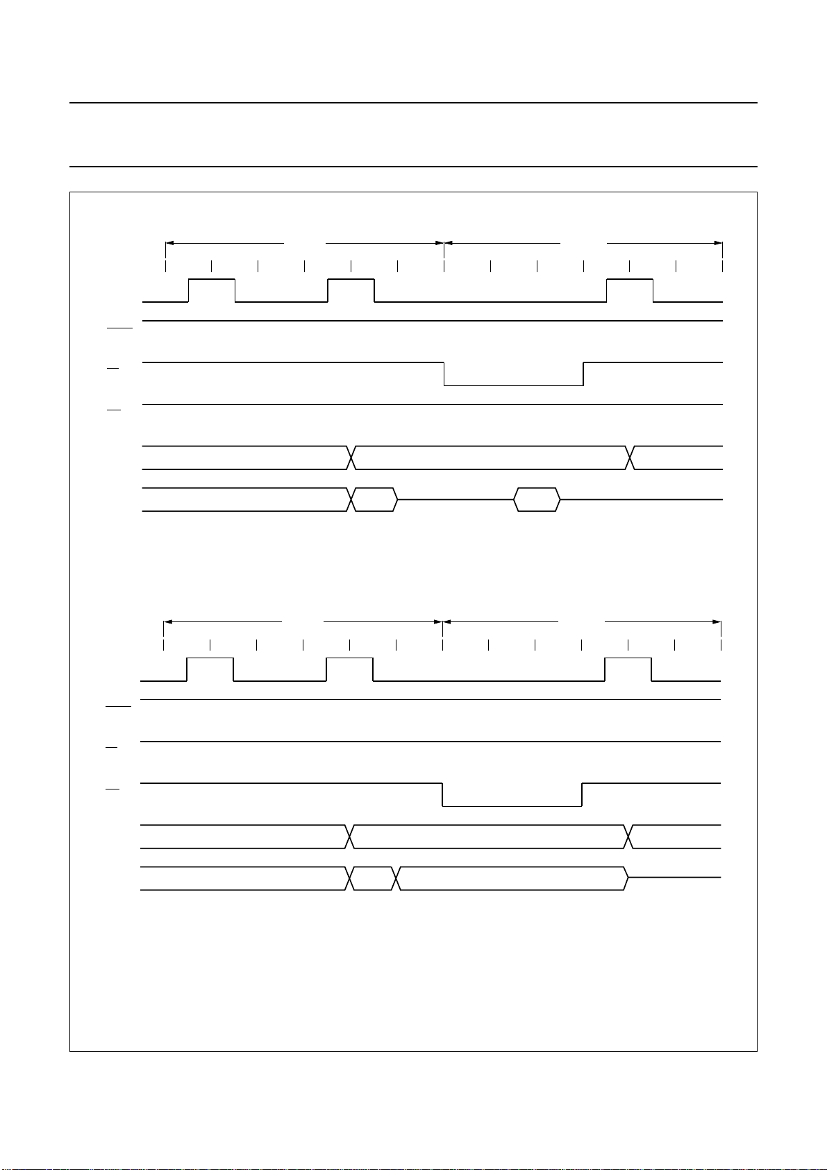
handbook, full pagewidth
ALE
PSEN
RD
WR
P2 PCH OUT
P0
handbook, full pagewidth
ALE
one machine cycle
S1 S2 S3 S4 S5 S6 S1 S2 S3 S4 S5 S6
PCH OUT PCH OUT PCH OUT PCH OUT
INST
IN
PCL
OUT
INST
IN
PCL
OUT
INST
IN
PCL
OUT
one machine cycle
INST
IN
PCL
OUT
a. Without a MOVX.
cycle 1
S1 S2 S3 S4 S5 S6 S1 S2 S3 S4 S5 S6
cycle 2
MBC461
PSEN
RD
WR
P2 PCH OUT
P0
P2
P0
INST
IN
PCH OUT PCH OUT ADDRH OUT PCH OUT
INST
IN
PCH OUT ADDRH OUT PCH OUT
PCL
OUT
PCL
OUT
INST
IN
INST
IN
ADDRL
OUT
ADDRL
OUT
(read)
DATA OUT
(write)
b. With a MOVX to the AUX-RAM (read and write).
Fig.9 External program memory execution.
PCL
OUT
PCL
OUT
MBC462
1997 Dec 15 17

Philips Semiconductors Product specification
8-bit microcontrollers P83C524; P80C528; P83C528
handbook, full pagewidth
ALE
PSEN
RD
WR
P2 PCH OUT
P0
handbook, full pagewidth
INST
cycle 1
S1 S2 S3 S4 S5 S6 S1 S2 S3 S4 S5 S6
PCH OUT DPH OUT PCH OUT
IN
PCL
OUT
INST
IN
DPL
OUT
DATA
IN
cycle 2
PCL
OUT
a. With a MOVX to the External Data Memory (read).
cycle 1
S1 S2 S3 S4 S5 S6 S1 S2 S3 S4 S5 S6
cycle 2
MBC463
ALE
PSEN
RD
WR
P2 PCH OUT
P0
INST
IN
PCH OUT DPH OUT PCH OUT
PCL
OUT
INST
IN
DPL
OUT
b. With a MOVX to the External Data Memory (write).
Fig.10 External program memory execution (continued).
1997 Dec 15 18
DATA OUT
PCL
OUT
MBC464
Philips Semiconductors Product specification
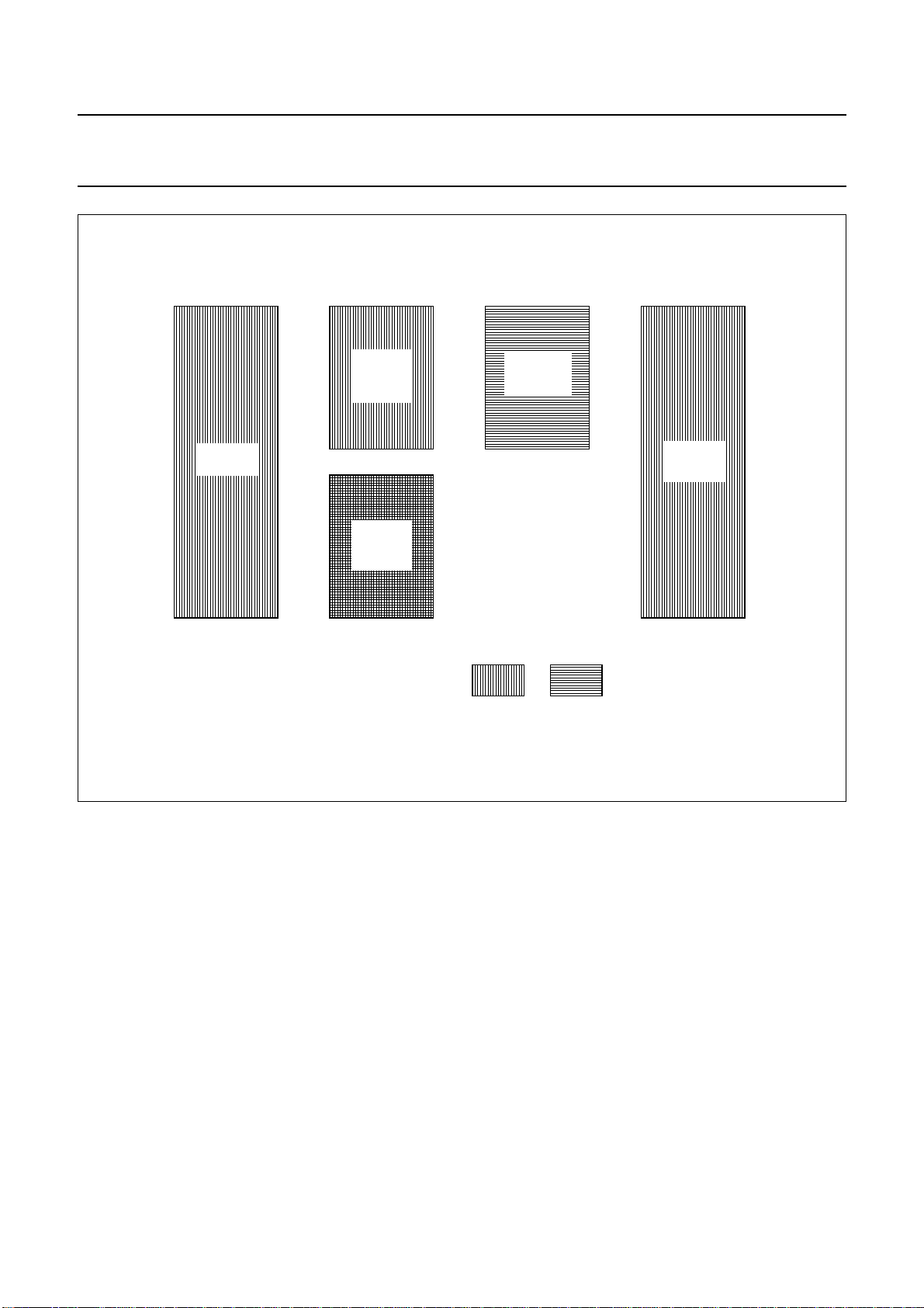
8-bit microcontrollers P83C524; P80C528; P83C528
SHARED
ADDRESS LOCATION
handbook, full pagewidth
FF
00
AUX - RAM
256 BYTES
FF FF
UPPER
128 BYTES
INTERNAL
RAM
80
7F
LOWER
128 BYTES
INTERNAL
RAM
00
register
indirect
addressing
FUNCTION
REGISTERS
80
DATA MEMORY
SPECIAL
FFFF
0100
direct byte
addressing
EXTERNAL
DATA
MEMORY
MBC466 - 1
Fig.11 Internal and external data memory address space.
1997 Dec 15 19

Philips Semiconductors Product specification
8-bit microcontrollers P83C524; P80C528; P83C528
handbook, full pagewidth
REGISTER
MNEMONIC
BIT MNEMONIC /
BIT ADDRESS (HEX)
F7 F6 F5 F4 F3 F2 F1 F0 F0HB
E7 E6 E5 E4 E3 E2 E1 E0
SCI/
SDI/
SCO
SDO
DF
CYD7ACD6FOD5RSID4RSOD3OVD2FID1P
TF2CFEXF2CERCLKCDTCLKCCEXEN2CBTR2
- - -BFPS1BEPT2BDPSBCPT1BBPX1BAPT0B9PX0
B7 B6 B5 B4 B3 B2 B1 B0
EAAFES1AEET2ADESACET1ABEX1AAET0A9EX0
CLHDOBBDCRBFDBWBFDASTRD9ENS
DE
CA
C/T2
C9
CP/RL2
DIRECT BYTE
ADDRESS (HEX)
FFHT3
E0HACC
DAHS1INT
D9HS1BIT
D8
D8HS1SCS
D0
D0HPSW
CDHTH2
CCHTL2
CBHRCAP2H
CAHRCAP2L
C8HT2CON
C8
B8
B8HIP
B0HP3
A8
A8HIE
A5HWDCON
SM09FSM19ESM29DREN9CTB89BRB89ATI99RI
97 96 95 94 93 92 91 90
TL1
TF18FTR18ETF08DTR08CIE18BIT18AIE089IT0
PCON
DPH
DPL
SP
87 86 85 84 83 82 81 80
Fig.12 Special Function Register (SFR) memory map.
1997 Dec 15 20
98
88
MBC465 - 1
A0HP2 A7 A6 A5 A4 A3 A2 A1 A0
99HSBUF
98HSCON
90HP1
8DHTH1
8CHTH0
8BH
8AHTL0
89HTMOD
88HTCON
87H
83H
82H
81H
80HP0

Philips Semiconductors Product specification
8-bit microcontrollers P83C524; P80C528; P83C528
9.3 Addressing
The P83C528 has five modes for addressing:
• Register
• Direct
• Register-Indirect
• Immediate
• Base-Register plus Index-Register-Indirect.
The first three methods can be used for addressing
destination operands. Most instructions have a
'destination/source' field that specifies the data type,
addressing methods and operands involved. For
operations other than MOVs, the destination operand is
also a source operand.
Access to memory addresses is as follows:
• Register in one of the four 8-bit register banks through
Register, Direct or Register-Indirect addressing.
• 512 bytes of internal RAM through Direct or
Register-Indirect addressing. Bytes 0-127 of internal
RAM may be addressed directly/indirectly. Bytes
128-255 of internal RAM share their address location
with the SFRs and so may only be addressed indirectly
as data RAM. Bytes 0-255 of AUX-RAM can only be
addressed indirectly via MOVX.
• SFR through Direct addressing at address locations
128-255.
• External data memory through Register-Indirect
addressing.
• Program memory look-up tables through Base-Register
plus Index-Register-Indirect addressing.
1997 Dec 15 21
Philips Semiconductors Product specification
h
8-bit microcontrollers P83C524; P80C528; P83C528
10 I/O FACILITIES
The P83C528 has four 8-bit ports. Ports 0-3 are the same
as in the 80C51, with the exception of the additional
function of Port 1. Port lines P1.0 and P1.1 may be used
as inputs for Timer 2, P1.1 may also be used as an
additional (third) external interrupt request input. Port lines
P1.6 and P1.7 may be selected as the SCL and SDA lines
of Serial Port SIO1 (I2C). Because the I2C-bus may be
active while the device is disconnected from VDD, these
pins are provided with open drain drivers. Pins P1.6 and
P1.7 do not have pull-up devices when used as ports.
Ports 0, 1, 2, and 3 perform the following alternative
functions:
• Port 0: provides the multiplexed low-order address and
data bus used for expanding the P83C528 with standard
memories and peripherals.
• Port 1: pins can be configured individually to provide:
external interrupt request input (external interrupt 2);
external inputs for Timer/counter 2; SCL and SDA for
the I2C interface.
• Port 2: provides the high-order address bus when
expanding the P83C528 with external program memory
and/or external data memory.
• Port 3: pins can be configured individually to provide:
external interrupt request inputs (external interrupt 0/1);
external inputs for Timer/counter 0 and
Timer/counter 1; Serial Port receiver input and
transmitter output control-signals to read and write
external data memory.
Bits which are not used for the alternative functions may be
used as normal bidirectional I/O pins. The generation or
use of a Port 1 or Port 3 pin as an alternative function is
carried out automatically by the P83C528 provided the
associated SFR bit is HIGH. Otherwise the port pin is held
at a logical LOW level.
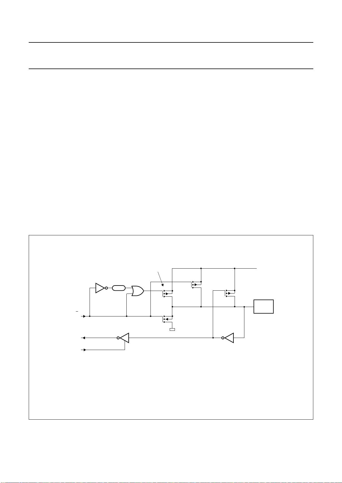
andbook, full pagewidth
2 oscillator
periods
from port latch
read port pin
Q
input data
strong pull-up
INPUT
BUFFER
p2
p1
n
p3
I1
+5 V
I/O PIN
PORT
MLA513
Fig.13 I/O buffers in the P83C528 (Ports 1, 2 and 3 except P1.6 and P1.7).
1997 Dec 15 22

Philips Semiconductors Product specification
8-bit microcontrollers P83C524; P80C528; P83C528
11 TIMERS/COUNTERS
The P83C528 contains three 16-bit timer/counters, Timer
0, Timer 1 and Timer 2, and one 8-bit timer, the Watchdog
Timer T3. Timer 0, Timer 1 and Timer 2 may be
programmed to carry out the following functions:
• measure time intervals and pulse durations
• count events
• generate interrupt requests.
11.1 Timer 0 and Timer 1
Timers 0 and 1 each have a control bit in TMOD SFR that
selects the timer or counter function of the corresponding
timer. In the timer function, the register is incremented
every machine cycle. Thus, one can think of it as counting
machine cycles. Since a machine cycle consists of 12
oscillator periods, the count rate is
frequency.
In the counter function, the register is incremented in
response to a HIGH-to-LOW transition at the
corresponding external input pin, T0 or T1. In this function,
the external input is sampled during S5P2 of every
machine cycle. When the samples show a HIGH in one
cycle and a LOW in the next cycle, the counter is
incremented. Thus, it takes two machine cycles (24
oscillator periods) to recognize a HIGH-to-LOW transition.
There are no restrictions on the duty cycle of the external
input signal, but to ensure that a given level is sampled at
least once before it changes, it should be held for at least
one full machine cycle.
1
⁄12 of the oscillator
When Timer 0 is in Mode 3, Timer 1 can be programmed
to operate in Modes 0, 1 or 2 but cannot set an interrupt
request flag and generate an interrupt. However, the
overflow from Timer 1 can be used to pulse the Serial Port
transmission-rate generator. With a 16 MHz crystal, the
counting frequency of these timer/counters is as follows:
• in the timer function, the timer is incremented at a
frequency of 1.33 MHz (oscillator frequency divided by
12).
• in the counter function, the frequency handling range for
external inputs is 0 Hz to 0.66 MHz.
Both internal and external inputs can be gated to the timer
by a second external source for directly measuring pulse
duration.
The timers are started and stopped under software control.
Each one sets its interrupt request flag when it overflows
from all logic 1's to all logic 0's (respectively, the automatic
reload value), with the exception of Mode 3 as previously
described.
Timer 0 and Timer 1 can be programmed independently to
operate in one of four modes:
Mode 0 8-bit timer/counter with divide-by-32 prescaler
Mode 1 16-bit timer/counter
Mode 2 8-bit timer/counter with automatic reload
Mode 3 Timer 0: one 8-bit timer/counter and one 8-bit
timer. Timer 1: stopped.
1997 Dec 15 23
 Loading...