
查询OM6213供应商
INTEGRATED CIRCUITS
DATA SH EET
OM6213
48 × 84 pixels matrix LCD driver
Product specification
File under Integrated Circuits, IC17
2001 Nov 07

Philips Semiconductors Product specification
48 × 84 pixels matrix LCD driver OM6213
CONTENTS
1 FEATURES
2 APPLICATIONS
3 GENERAL DESCRIPTION
4 ORDERING INFORMATION
5 BLOCK DIAGRAM
6 PINNING
7 PIN FUNCTIONS
7.1 ROW 0 to ROW 47 row driver outputs
7.2 COL 0 to COL 83 column driver outputs
7.3 V
7.4 V
7.5 V
and V
SS1
DD1
LCDOUT, VLCDIN
to V
SS2
: positive power supply rails
DD3
: negative power supply rails
and V
LCDSENSE
: LCD power
supplies
7.6 V
OS0
to V
OS4
7.7 T1 to T7: test pads
7.8 SDIN: serial data line
7.9 SCLK: serial clock line
7.10 D/C: mode select
7.11 SCE: chip enable
7.12 OSC: oscillator
7.13 RES: reset
8 BLOCK DIAGRAM FUNCTIONS
8.1 Oscillator
8.2 Address counter (AC)
8.3 Display Data RAM (DDRAM)
8.4 Timing generator
8.5 Display address counter
8.6 LCD row and column drivers
8.7 V
generator
LCD
9 INITIALIZATION
10 ADDRESSING
10.1 Data structure
11 INSTRUCTIONS
11.1 Reset function
11.2 Function set
11.2.1 PD
11.2.2 V
11.2.3 H
11.3 Display Control
11.3.1 D, E
11.4 Set Y address of RAM
11.5 Set X address of RAM
11.6 Temperature Control
11.7 Bias value:
11.8 V
generator
LCD
12 TEMPERATURE COMPENSATION
13 LIMITING VALUES
14 HANDLING
15 DC CHARACTERISTICS
16 AC CHARACTERISTICS
17 SERIAL INTERFACE
18 RESET
19 APPLICATION INFORMATION
20 MODULE MAKER PROGRAMMING
20.1 V
calibration
LCD
20.2 Charge pump multiplication factor
20.3 Bias system selected when BS[2:0] = 100
20.4 V
temperature coefficient selected when
LCD
TC[1:0] = 01 (TC1)
20.5 Seal bit
20.6 Module Maker parameter programming
20.7 Example of V
calibration flow
LCD
21 CHIP INFORMATION
22 BONDING PAD LOCATIONS
23 DEVICE PROTECTION DIAGRAM
24 TRAY INFORMATION
25 DEFINITIONS
26 LIFE SUPPORT APPLICATIONS
2001 Nov 07 2

Philips Semiconductors Product specification
48 × 84 pixels matrix LCD driver OM6213
1 FEATURES
• Single-chip LCD controller/driver
• 48 row, 84 column outputs
• Display data RAM 48 × 84 bits
• On-chip:
– Generation of LCD supply voltage (external supply
also possible)
– Generation of intermediate LCD bias voltages
– Oscillator requires noexternal components (external
clock also possible).
• External reset (RES) input pin
• Serial interface maximum 4.0 Mbit/s
• CMOS compatible inputs
• Mux rate: 1 : 48
• Logic supply voltage range V
• Supply voltage range for high voltage part V
to VSS: 2.5 to 3.3 V
DD1
DD2
to VSS:
2.5 to 3.3 V
• Display supply voltage range V
to VSS: 4.5 to 9.0 V
LCD
• Low power consumption (typically 120 µA), suitable for
battery operated systems
• Temperature compensation of V
• Temperature range: T
amb
LCD
= −40 to +85 °C
• 5 Module Maker programmable parameters.
2 APPLICATIONS
• Telecommunications equipment.
3 GENERAL DESCRIPTION
The OM6213 is a low power CMOS LCD controller driver,
designed to drive a graphic display of 48 rows and
84 columns. All necessary functions for the display are
provided in a single chip, including on-chip generation of
LCD supply and bias voltages, resulting in a minimum of
external components and low power consumption. The
OM6213 interfaces to microcontrollers via a serial bus
interface.
4 ORDERING INFORMATION
PACKAGE
TYPE NUMBER
NAME DESCRIPTION VERSION
OM6213U TRAY chip with bumps in tray −
2001 Nov 07 3
Philips Semiconductors Product specification
48 × 84 pixels matrix LCD driver OM6213
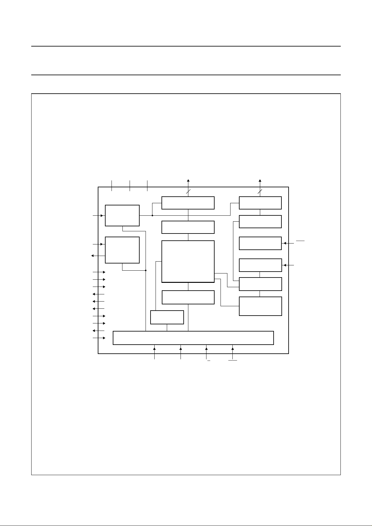
5 BLOCK DIAGRAM
V
handbook, full pagewidth
DD1
V
DD2VDD3
COL 0 to COL 83
ROW 0 to ROW 47
V
LCDIN
V
LCDSENSE
V
LCDOUT
V
V
V
OS
SS1
SS2
[
4:0
T1
T2
T3
T4
T5
T6
T7
]
BIAS
VOLTAGE
GENERATOR
V
LCD
GENERATOR
COLUMN DRIVERS
DATA LATCHES
DISPLAY DATA RAM
(DDRAM)
48 × 84 bits
ADDRESS COUNTER
DATA
REGISTER
SDIN SCLK
84
I/O BUFFER
OM6213
D/C
ROW DRIVERS
SHIFT REGISTER
OSCILLATOR
GENERATOR
SCE
48
RESET
TIMING
DISPLAY
ADDRESS
COUNTER
RES
OSC
MGT840
Fig.1 Block diagram.
2001 Nov 07 4

Philips Semiconductors Product specification
48 × 84 pixels matrix LCD driver OM6213
6 PINNING
SYMBOL PAD DESCRIPTION
V
V
V
V
V
V
V
V
OS4
OS3
OS2
OS1
OS0
DD1
DD3
DD2
3V
4V
5V
6V
7V
13 to 18 supply voltage 1
19 to 22 supply voltage 3
23 to 30 supply voltage 2
offset pad 0 input
LCD
offset pad 1 input
LCD
offset pad 2 input
LCD
offset pad 3 input
LCD
offset pad 4 input
LCD
SCLK 31 serial clock input
T7 32 to 35 test 7 alternative HV-gen
programming input
SDIN 36 to 39 serial data input and HV-gen
programming input
D/
C 40 data/command input
SCE 41 chip enable input (active
LOW)
OSC 42 oscillator input
V
SS2
43 to 50 ground 2
T4 51 test 4 input
T5 52 test 5 input
T6 53 test 6 output
V
SS1
54 to 61 ground 1
SYMBOL PAD DESCRIPTION
T1 62 test 1 output
T2 63 test 2 output
T3 64 test 3 output
V
LCDIN
65 to 70 V
supply voltage input and
LCD
HV-gen programming input
V
LCDOUT
V
LCDSENSE
71 to 77 V
78 V
generator output
LCD
generator regulation
LCD
input
RES 79 reset input (active LOW)
ROW 11 to
89 to 100 LCD row driver outputs
ROW 0
ROW 12 to
101 to 112 LCD row driver outputs
ROW 23
COL 0 to
113 to 196 LCD column driver outputs
COL 83
ROW 47 to
197 to 208 LCD row driver outputs
ROW 36
ROW 24 to
209 to 220 LCD row driver outputs
ROW 35
1,8 to 12,
dummy pads
81 to 88,
221 and
222
7 PIN FUNCTIONS
7.1 ROW 0 to ROW 47 row driver outputs
These pads output the row signals.
7.2 COL 0 to COL 83 column driver outputs
These pads output the column signals.
7.3 V
V
SS1
SS1
andV
and V
mustbe connected together, jointly referred
SS2
: negative power supply rails
SS2
to as VSS. When a pin has to be connected externally to
VSS, V
7.4 V
V
DD1
analog supply; jointly referred to as V
should be used.
SS1
DD1
to V
: positive power supply rails
DD3
provides the logic supply. V
DD2
and V
DD2
. V
DD3
DD2
provide the
and V
DD3
must be connected together.
2001 Nov 07 5
7.5 V
LCDOUT, VLCDIN
and V
LCDSENSE
: LCD power
supplies
If the internal V
be connected together. If not (the internal V
generator is used, then all 3 pins must
LCD
LCD
generator
is disabled and an external voltage is supplied at pin
V
), V
LCDIN
LCDOUT
must be connected to V
switch-off the charge pump if an external V
is used. V
7.6 V
LCDIN
OS0
Five input pins for on-glass V
connected to V
V
, which corresponds to logic 1. All five pins define a
DD1
must be left open-circuit and V
LCDIN.VPR
must be set to logic 0to
generator
LCD
is also used for HV-gen programming.
to V
OS4
offset. Each pin must be
LCD
, which corresponds to logic 0, or to
SS1
LCDSENSE
5-bit two’s complement number ranging from −16 to +15
decimal (from 10000 to 01111). The default value, with all
pins connected to V
, is 0 decimal (00000). The register
SS1
is refreshed by each set bias system command or when
exiting the Power-down mode.

Philips Semiconductors Product specification
48 × 84 pixels matrix LCD driver OM6213
7.7 T1 to T7: test pads
In the application, T4, T5 and T7 must be connected to
VSS. T1, T2, T3 and T6 must be left open-circuit.
7.8 SDIN: serial data line
Data line and HV-gen programming input.
7.9 SCLK: serial clock line
Input for the clock signal. 0 to 4.0 Mbits/s.
7.10 D/C: mode select
Input to select either command/address or data input.
7.11 SCE: chip enable
The enable pin allows data to be clocked in; this signal is
active LOW.
7.12 OSC: oscillator
If the on-chip oscillator is used, this input must be
connected to V
connected to pin OSC. If pin OSC is left at V
. If an external clock is used, it must be
DD1
, the
SS1
internal clock isdisabled, the deviceis not clocked and the
display may be left in a DC state. To avoid this, it is
advisable to enter the Power-down mode before stopping
the clock.
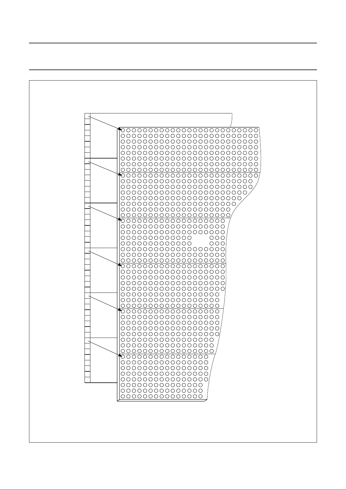
8.3 Display Data RAM (DDRAM)
The OM6213 contains a 48 × 84 bit static RAM which
storesthe display data.The RAM is dividedinto 6 banks of
84 bytes (6 × 8 × 84 bits). During RAM access, data is
transferred to the RAM via the serial interface. There is a
direct correspondence between the X address and the
column output number.
8.4 Timing generator
The timing generator produces the various signals
required to drive the internal circuitry. Internal chip
operation is not affected by operations on the data bus.
8.5 Display address counter
The display is generated by continuously shifting rows of
RAM data to the dot matrix LCD via the column outputs.
The display status (all dots on/off and normal/inverse
video) is set by bits D and E in the command ‘Display
control’ (see Table 2).
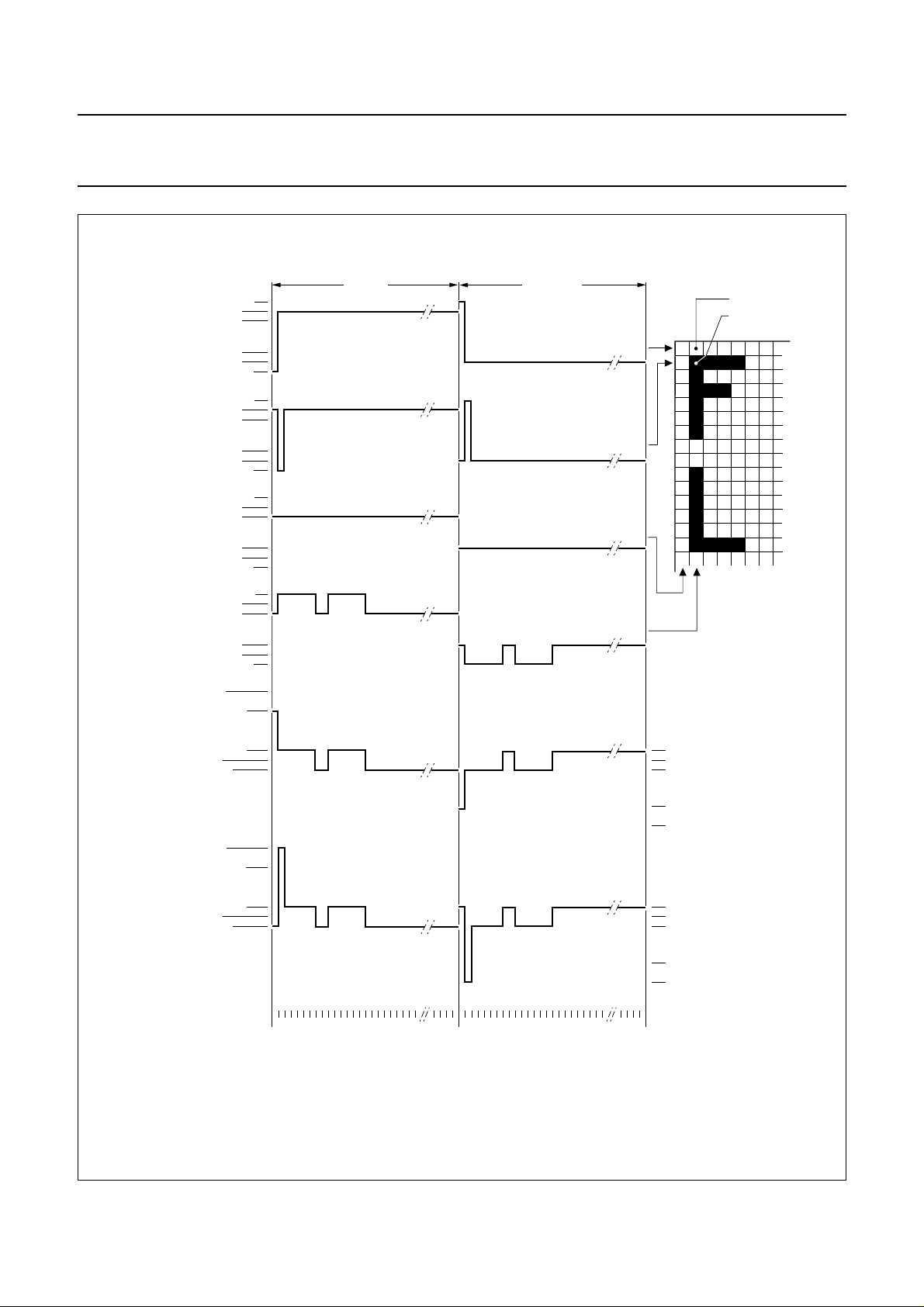
8.6 LCD row and column drivers
The OM6213 contains 48 rows and 84 column drivers,
which connect the appropriate LCD bias voltages in
sequence to the display in accordance with the data to be
displayed. Figure 2 shows typical waveforms. Unused
outputs should be left unconnected.
7.13 RES: reset
This signal will reset the device and must be applied to
properly initialize the chip; this signal is active LOW.
8 BLOCK DIAGRAM FUNCTIONS
8.1 Oscillator
The on-chip oscillator provides the clock signal for the
display system. No external components are required and
the OSC input must be connected to V
. If an external
DD1
clock signal is used, it must be connected to pin OSC.
8.2 Address counter (AC)
The address counter assigns addresses to the display
data RAM for writing. The X address X[6:0] and the
Y addressY[2:0] are set separately. Afterawrite operation
the address counter is automatically incremented by 1
according to the V flag.
8.7 V
generator
LCD
The voltage multiplier (i.e. charge pump) generates the
V
voltage. The multiplication factor is Module Maker
LCD
programmable (default value 4).
2001 Nov 07 6
Philips Semiconductors Product specification
48 × 84 pixels matrix LCD driver OM6213
ROW 0
R0 (t)
ROW 1
R1 (t)
COL 0
C0 (t)
COL 1
C1 (t)
V
V3 − V
LCD
V
V
V
V
V
V
V
V
V
V
V
V
V
V
V
V
V
V
V
V
V
V
V
V
SS1
LCD
2
3
4
5
SS1
LCD
2
3
4
5
SS1
LCD
2
3
4
5
SS1
LCD
2
3
4
5
SS1
frame n frame n + 1
V
state1
V
state2
(t)
(t)
V
state1
V
state2
(t) = C1(t) − R0(t)
V
state1
V
(t) = C1(t) − R1(t)
state2
V
− V
LCD
0 V
V3 − V
V
LCD
V3 − V
V
LCD
0 V
V3 − V
2
SS1
− V
2
2
2
012345678... ... 47 012345678... ... 47
(t)
(t)
V4 − V
0 V
V
SS1
V4 − V
− V
LCD
V4 − V
0 V
V
SS1
V4 − V
− V
LCD
MGT841
5
− V
LCD
5
− V
LCD
5
5
Fig.2 Typical LCD driver waveforms.
2001 Nov 07 7
Philips Semiconductors Product specification
48 × 84 pixels matrix LCD driver OM6213
DDRAM
bank 0
top of LCD
R0
bank 1
R8
bank 2
bank 3
bank 4
bank 5
R16
LCD
R24
R32
R40
Fig.3 DDRAM to display mapping.
2001 Nov 07 8
R47
MGT842
Philips Semiconductors Product specification
48 × 84 pixels matrix LCD driver OM6213
9 INITIALIZATION
Immediately following power-on, all internal registers and
the RAM content are undefined. A reset (RES)pulse must
be applied. It should be noted that the device may be
damaged if not properly reset.
Reset is accomplished by applying an external RES pulse
(active LOW) at pad RES. When reset occurs within the
specified time, all internal registers are reset, however the
RAM is still undefined. The state after reset is described in
Section “Reset function”.
RES input must be ≤ 0.3V
V
(or higher) according to t
DD(min)
DD1
after V
VHRL
reaches
DD1
timing (see
Fig.16).
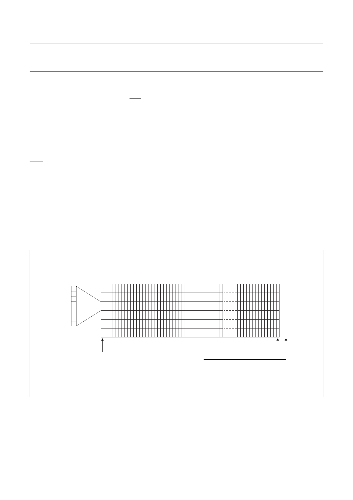
10 ADDRESSING
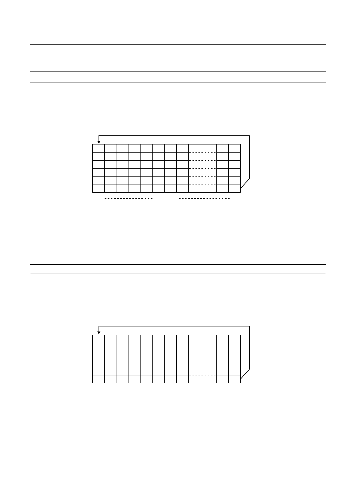
Data is downloaded in bytes into the RAM matrix of the
OM6213 as indicated in Figs.3, 4, 5 and 6. The display
RAM has a matrix of 48 × 84 bits. The columns are
addressed by the address pointer.
10.1 Data structure
The address ranges are: X=0to83 (1010011) and
Y = 0 to 5 (101). Addresses outside these ranges are not
allowed.
In vertical addressing mode (V = 1) the Y address
increments after each byte (see Fig.5). After the last
Y address (Y = 5) Y wraps around to 0 and X increments
to address the next column.
In horizontal addressing mode (V = 0) the X address
increments after each byte; see Fig.6. After the last
X address (X = 83) X wrapsaround to 0 andY increments
to address the next row.
After the very last address (X = 83 and Y = 5) the address
pointers wrap around to address (X = 0 and Y = 0).
handbook, full pagewidth
LSB
MSB
0 83X address
Y address
Fig.4 RAM format, addressing.
0
5
MGT843
2001 Nov 07 9
Philips Semiconductors Product specification
48 × 84 pixels matrix LCD driver OM6213
handbook, full pagewidth
06
17
2
3
4
5
083X address
0
Y address
5503
MGT844
Fig.5 Sequence of writing data bytes into RAM with vertical addressing (V = 1).
handbook, full pagewidth
012
84 85 86
168 169 170
252 253 254
336 337 338
420 421 422
083X address
Fig.6 Sequence of writing data bytes into RAM with horizontal addressing (V = 0).
2001 Nov 07 10
0
Y address
5503
MGT845

Philips Semiconductors Product specification
48 × 84 pixels matrix LCD driver OM6213
11 INSTRUCTIONS
The instruction format is divided into two modes. If D/C
(mode select) isset LOW the current byte is interpretedas
command byte (see Table 1). If D/C is set HIGH the
following bytes are stored in the DDRAM. After every data
byte the address counter is incremented automatically.
The level of the D/C signal is read during the last bit of the
data byte.
Instructions can be sent in any order to the OM6213 (the
exception being that the temperature control command
mustbefollowed by at least onebyteofdata or command).
TheMSBis transmitted first (see Fig.7).Figure 8showsan
example of a command stream, used to set-up the LCD
driver.
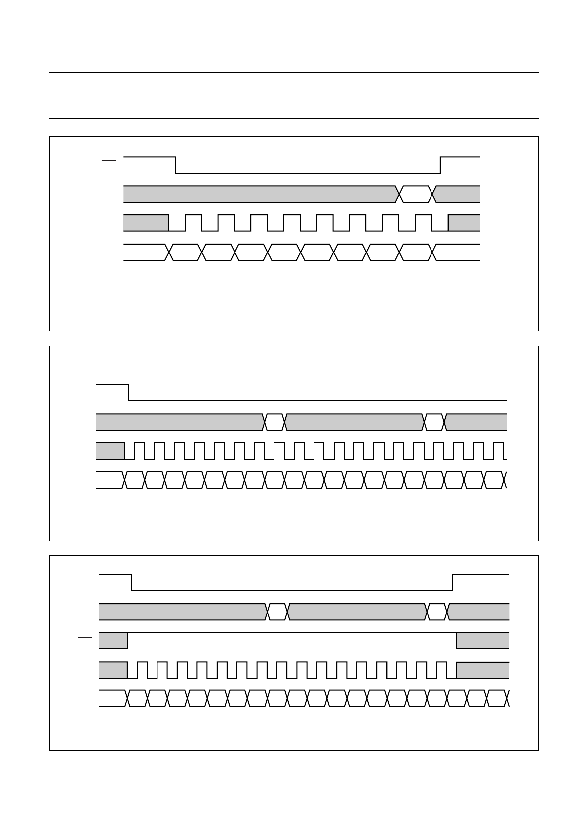
The serial interfaceis initialized whenSCE is HIGH. In this
state SCLK clock pulses have no effect and no power is
consumedby the serialinterface. A negativeedge on SCE
enablestheserial interface and indicates the startofadata
transmission.
Figures 9 and 10 show the serial bus protocol.
• When SCE is HIGH, SCLK clocks are ignored. During
the HIGH time of SCE the serial interface is initialized
(see Fig.11).
• SDIN is sampled at the positive edge of SCLK
• D/C indicates whether the byte is a command (D/C=0)
or RAM data (D/C = 1). It is read with the eighth SCLK
pulse.
• If SCE stays LOW after the last bit of a command/data
byte,the serial interfaceexpects bit DB7 ofthe next byte
at the next rising edge of SCLK (see Fig.11)
• A reset pulse with RES interrupts the transmission. The
data being written into the RAM may be corrupted. The
registers are cleared. If SCE is LOW after the rising
edge of RES, the serial interface is ready to receive the
D/C bit of a command/data byte (see Fig.12).
• Instructions (except the temperature control command)
are executed on the SCLK positive edge which latches
DB0 and D/C
• The temperature control command is executed on the
SCLK positive edge which latches DB0 and D/C of the
next command or the next write to the DDRAM
(whichever occurs first).This command requires 2 bytes
to be executed.
handbook, full pagewidth
handbook, halfpage
MSB (DB7) LSB (DB0)
Fig.7 General format of data stream.
bias systemfunction set (H = 1)
datadata
MGT639
set V
PR
temperature control
Fig.8 Serial data stream, example.
X addressY addressdisplay controlfunction set (H = 0)
MGT846
2001 Nov 07 11
Philips Semiconductors Product specification
48 × 84 pixels matrix LCD driver OM6213
handbook, full pagewidth
handbook, full pagewidth
SCE
D/C
SCLK
SDIN
SCE
D/C
DB7 DB6 DB5 DB4 DB3 DB2 DB1 DB0
MGT641
Fig.9 Serial bus protocol; transmission of one byte.
SCLK
SDIN DB7 DB6 DB5 DB4 DB3 DB2 DB1 DB0 DB7DB7 DB6 DB5 DB4 DB3 DB2 DB1 DB0
Fig.10 Serial bus protocol; transmission of several bytes.
handbook, full pagewidth
SCE
D/C
RES
SCLK
SDIN DB7 DB6 DB5 DB4 DB3 DB2 DB1 DB0 DB7DB7 DB6 DB5 DB4 DB3 DB2 DB1 DB0
Fig.11 Serial bus reset function (SCE).
DB6 DB5
MGT642
DB6 DB5
MGT643
2001 Nov 07 12
 Loading...