
INTEGRATED CIRCUITS
DATA SH EET
OM5193H
Disk drive spindle and VCM with
servo controller
Product specification
File under Integrated Circuits, IC11
1998 Nov 02

Philips Semiconductors Product specification
Disk drive spindle and VCM with
servo controller
CONTENTS
1 FEATURES
1.1 Servo control
1.2 Motor control
1.2.1 Spindle motor driver
1.2.2 Voice coil motor driver
1.3 Miscellaneous items
2 APPLICATIONS
3 GENERAL DESCRIPTION
3.1 Overview
3.2 Servo controller
3.3 Spindle and voice coil motor
3.4 Safety functions
4 QUICK REFERENCE DATA
5 ORDERING INFORMATION
6 BLOCK DIAGRAMS
7 PINNING
8 FUNCTIONAL DESCRIPTION
8.1 Serial interface
8.2 Commutation and sleep mode
8.3 Commutation control
8.3.1 Blanks, Watchdog and Start-up delays
8.3.2 Comdelim delay
8.4 10-bit ADC with 7 analog inputs
8.4.1 Input channels
8.4.2 Input ranges
8.4.3 Conversion modes
8.4.4 Programming register#0
8.4.5 Converter clock frequency values
8.5 10-bit VCM DAC
8.6 Reference voltage
8.7 Stand-alone op-amps
8.8 Analog switch
8.9 Charge pump voltage
8.10 Spindle driver
8.11 VCM driver
8.12 Park the VCM
8.13 Precharge the VCM
8.14 Brake the motor
8.15 Power-on reset
8.16 Thermal monitor and shutdown
8.17 Power supply isolation
8.17.1 External isolation diode
8.17.2 External power FET
8.18 Thermal behaviour
OM5193H
9 LIMITING VALUES
10 HANDLING
11 THERMAL CHARACTERISTICS
12 CHARACTERISTICS
13 APPLICATION INFORMATION
14 PACKAGE OUTLINE
15 SOLDERING
15.1 Introduction
15.2 Reflow soldering
15.3 Wave soldering
15.4 Repairing soldered joints
16 DEFINITIONS
17 LIFE SUPPORT APPLICATIONS
1998 Nov 02 2

Philips Semiconductors Product specification
Disk drive spindle and VCM with
servo controller
1 FEATURES
1.1 Servo control
• 10-bit VCM Digital-to-Analog Converter (DAC)
• 7-channel 10-bit Analog-to-Digital Converter (ADC)
• Programmable spindle commutation control logic
• 3-wire serial interface
• Two stand-alone operational amplifiers (op-amps) with
outputs connected to the ADC
• Analog multiplexer with two inputs used to select VCM
seek mode or track-following mode.
1.2 Motor control
1.2.1 S
• 3-phase output motor driver
• 1.9 A maximum available start-up current
• Total R
• Back ElectroMotive Force (BEMF) processing for
sensorless motor commutation
• Linear current control
• External current sense resistor
• External current control loop compensation
• Adjustable slew rate control
• Short-circuit brake
• Adjustable brake-after-park delay time.
1.2.2 V
• 1.5 A maximum current capability
• Total R
• Linear class AB output with low cross-over distortion
delay
• Precision current control loop with external current
sense resistor
• Programmable seek and track-following mode with
adjustable current loop gain
• External current control loop compensation
• Precharge during brake mode
• 20 kHz current control loop bandwidth
• Parking function
• Adjustable park voltage with limiter.
PINDLE MOTOR DRIVER
= 0.6 Ω (typical) at 25 °C
ds(on)
OICE COIL MOTOR DRIVER
= 0.8 Ω (typical) at 25 °C
ds(on)
OM5193H
1.3 Miscellaneous items
• Precision low voltage 5 and 12 V power monitor with
hysteresis
• Precision internal voltage reference for servo and power
control circuits
• Thermal sense circuit with over-temperature shutdown
sensor
• Internal charge pump voltage generator
• Automatic brake-after-park at power-down, thermal
shutdown or sleep mode
• Sleep mode: low power consumption mode.
2 APPLICATIONS
• 12 V hard disk drive products.
3 GENERAL DESCRIPTION
3.1 Overview
The OM5193H is a combination of a voice coil motor and
a spindle motor driver with embedded servo controller
designed for use in disk drives. Configuration and control
registers are set via a 3-wire serial port running up to
30 MHz to interface commonly to a microcontroller or a
digital signal processor.
The device operates at 5 and 12 V power supplies and
integrates safety functions such as power stages
overvoltage protection, power and temperature monitor,
over-temperature shutdown and dynamic
brake-after-park.
The device is contained in a QFP80 package with 18 pins
connected to the leadframe thus providing low thermal
resistance.
3.2 Servo controller
The servo controller includes the following circuits:
• 3-wire serial interface
• Spindle commutation logic
• A 10-bit ADC with 7 inputs selected by an internal
multiplexer
• A 10-bit VCM DAC with 1.5, 2.5 and 3.5 V voltage
references
• Two low-offset stand-alone op-amps
• Analog multiplexer with 2 inputs.
1998 Nov 02 3

Philips Semiconductors Product specification
Disk drive spindle and VCM with
servo controller
The serial interface is used:
• To adjust the timing parameters for proper spindle
commutation sequence
• To accurately adjust head positioning via the 10-bit VCM
DAC
• To set VCM seek or track-following mode via the
low-impedance switch
• To select and process analog signals via a 7-channel
multiplexer connected to the 10-bit ADC.
The spindle commutation logic circuit ensures proper
spindle start-up (no reverse rotation) and commutation
sequence for the spindle driver by processing BEMF
sensing circuit output signals.
The two stand-alone op-amps, with the inputs connected
to the read channel IC, provide servo track signals
processed by the microcontroller to perform accurate
track-following mode.
3.3 Spindle and voice coil motor
OM5193H
3.4 Safety functions
The OM5193H is protected against transient voltage
spikes that are generated by the inductive loads of spindle
and VCM.
Power supplies and temperature are monitored in order to
guarantee data reliability and self-protection of the device
in case of power loss or temperatures beyond maximum
rating.
Park and brake functions secure heads and disk media in
case of power-down or high temperature failure. This
function is also activated by the sleep mode.
An internal temperature monitor is available to monitor the
chip temperature and thus prevents over-temperature
shutdown. Internally connected to the ADC channel 4, it
can be used by the microcontroller as an early
‘temperature-too-high’ warning during a long VCM seek
sequence.
The OM5193H drives a 3-phase brushless, sensorless DC
spindle motor and a voice coil motor.
Spindle and voice coil motor power stages with low R
and high current capability are suitable for mid-end and
low-end 12 V disk drives. Power stages are designed in
such a way that external Schottky diodes are not needed.
Spindle current is sensed by an external resistor and
monitored by the external signal SPCC (SPindle Current
Control). Spindle speed is regulated by the microcontroller
via the ZCROSS signal (Zero CROSSing detection
frequency output). BEMF comparators provide the digital
zero crossing signals. These are processed by the
commutation logic circuit to properly switch-on and
switch-off spindle power drivers thus ensuring the rotation
of the motor.
The control of the heads positioning is accomplished by
the internal 10-bit VCM DAC. Seek and track-following
VCM current loop gain is set by external resistors. VCM
zero current is referenced to the 2.5 V internal voltage
reference.
An internal precharge of the actuator (magnetic latch)
during brake mode guarantees total control of the current
when VCM starts running without current spikes.
ds(on)
1998 Nov 02 4

Philips Semiconductors Product specification
Disk drive spindle and VCM with
OM5193H
servo controller
4 QUICK REFERENCE DATA
SYMBOL PARAMETER MIN. TYP. MAX. UNIT
Supply voltage
V
DDA1
V
DDD
V
DDA2
Drivers
I
SPOUT
I
VCMRUN
5 ORDERING INFORMATION
TYPE
NUMBER
OM5193H QFP80 plastic quad flat package; 80 leads (lead length 1.95 mm);
5 V analog supply voltage 4.5 5.0 5.5 V
5 V digital supply voltage 4.5 5.0 5.5 V
12 V analog supply voltage 10.8 12.0 13.2 V
spindle start-up current −−1.9 A
VCM current −−1.5 A
PACKAGE
NAME DESCRIPTION VERSION
SOT318-2
body 14 × 20 × 2.8 mm
1998 Nov 02 5
Philips Semiconductors Product specification
Disk drive spindle and VCM with
OM5193H
servo controller
6 BLOCK DIAGRAMS
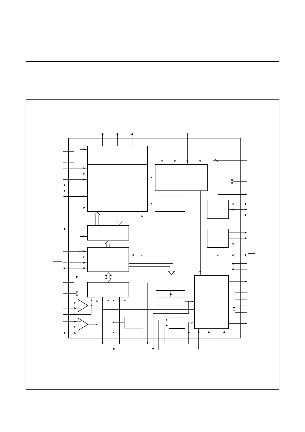
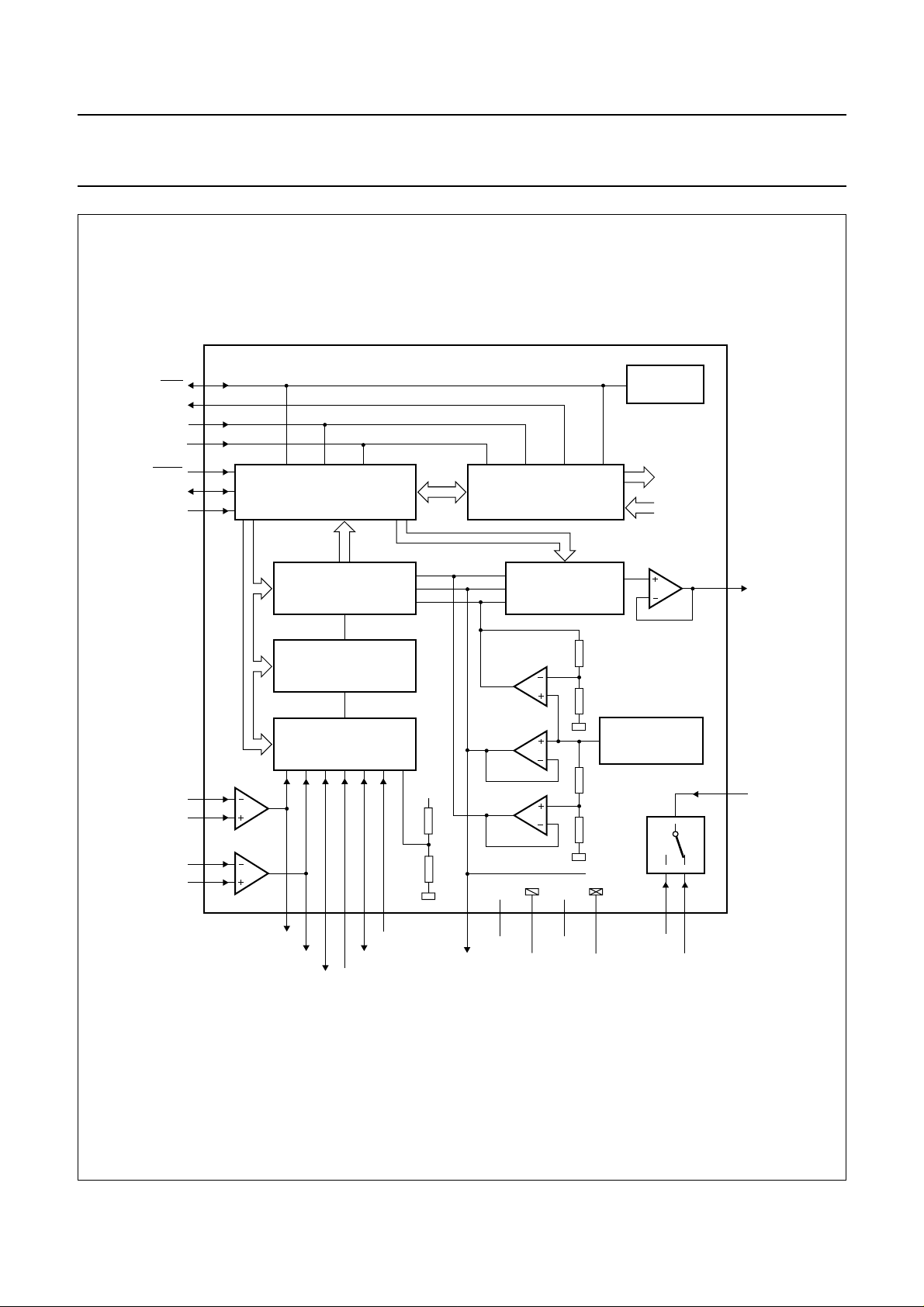
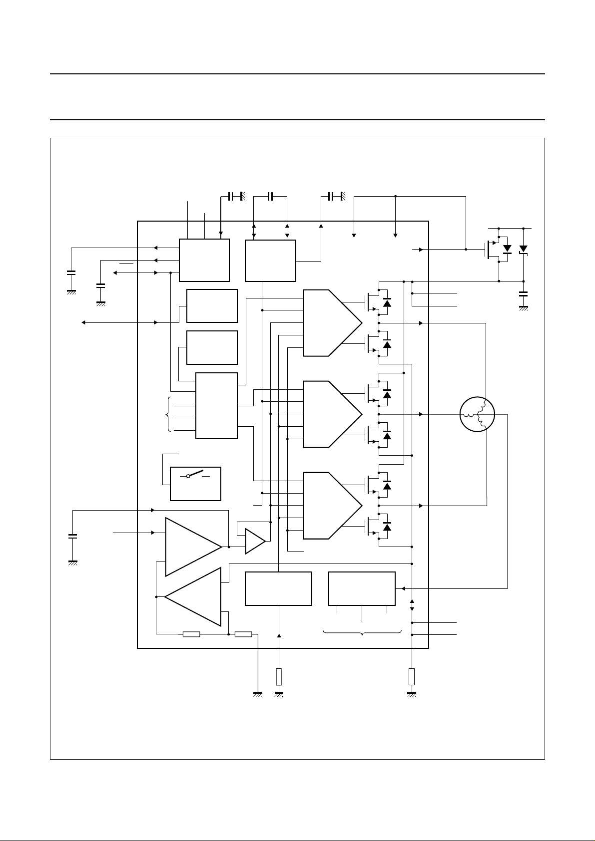
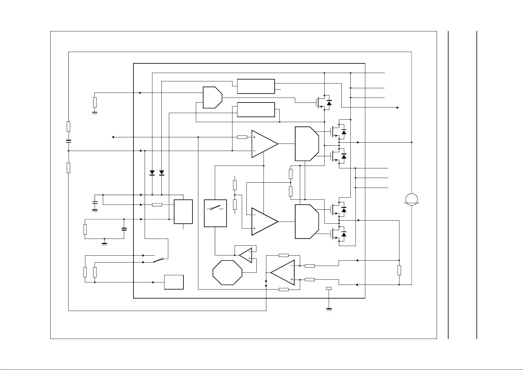
Figures 1, 2, 3 and 4 provide block diagrams of the OM5193H servo and motor control (top level diagram, servo
controller, spindle motor driver and voice coil motor driver).
handbook, full pagewidth
CLAMP1
CLAMP2
CLAMP3
SLEW
SPCCOUT
SPCC
MOTSENSE3
MOTSENSE2
MOTSENSE1/
SPSENSEH
GNDS/SPSENSEL
ZCROSS
CLOCK
SCLOCK
SDEN
SDATA
SCANTEST
V
DDA1
V
DDA2
AGND
INTINN
INTIN
ADC[0]/INTOUT
PESAMPN
PESAMP
ADC[1]/DIFOUT
CT
10
55
56
12
14
13
73
76
2
11
9
25
24
23
21
22
26
44
15
39
37
38
28
35
36
29
CLAMP
A2
A1
MOTA
72
SPINDLE
CONTROL
COMA
COMB
COMC
COMMUTATION
LOGIC
SERIAL
INTERFACE
7-CHANNEL
10-BIT ADC
0 1 2 3 4 5 6
30 31 32 33 34 40 42 41 43 53 52
ADC[2]/SOUT
ADC[3]
MOTB
74
POWER
STAGE
ACROSS
BCROSS
CCROSS
THERMAL
MONITOR
ADC[5]
ADC[4]/TEMP
BRAKEDELAY
MOTC
BRAKEPOWER
3 48 50 49 51
PARK AND BRAKE
THERMAL
SHUTDOWN
OM5193H
10-BIT
VCM DAC
0.5V
DDA1
DACOUT
REF2V5
BANDGAP
VCM
SWITCH
SEEKSELECT
TRACKFWSELECT
PARKVOLT
BRAKEADJH
VCMIN
VCMSENSEL
VCM
CONTROL
VCMSENSEH
1, 4 to 7,
58 to 61, 64 to 67,
70, 75, 78 to 80
18
CHARGE
PUMP
POWER-ON
RESET
POWER
STAGE
CLAMP
20
27
16
17
18
46
47
45
19
57
77
69
71
68
63
54
62
MGM972
8
HEATSINK
V
DDD
DGND
SWITCHGATE
BSTCP1
BSTCP2
CAPY
CHK5
CHK12
CPOR
POR
PWRBIAS1
PWRBIAS2
NIVCM
GNDVCM1
GNDVCM2
GNDVCM3
GNDV
IVCM
Fig.1 Block diagram, top level.
1998 Nov 02 6
Philips Semiconductors Product specification
Disk drive spindle and VCM with
servo controller
handbook, full pagewidth
POR
ZCROSS
CLOCK
SCANTEST
SDEN
SDATA
SCLOCK
19
25
24
26
21
22
23
SERIAL INTERFACE COMMUTATION LOGIC
10-BIT ADC
10-BIT VCM DAC
POWER-ON
RESET
COMA
COMB
COMC
ACROSS
BCROSS
CCROSS
OM5193H
34
DACOUT
INTINN
INTIN
PESAMPN
PESAMP
37
A2
38
35
A1
36
ADC[0]/INTOUT
ADC[1]/DIFOUT
ADC[2]/SOUT
RANGE
ADAPTER
INPUT
MULTIPLEXER
30 31 32 33
29
28
ADC[5]
ADC[4]/TEMP
ADC[3]
V
DDA1
V
ref3V5
V
ref2V5
V
ref1V5
V
ref2V5
40 39
V
REF2V5
44
DDA1
AGND DGND
V
20
DDD
OM5193H
2.5 V BANDGAP
VCM switch
for VCM
27
SEEKSELECT
TRACKFWSELECT
VCMIN
414342
MGM973
Fig.2 Block diagram, servo controller.
1998 Nov 02 7
Philips Semiconductors Product specification
Disk drive spindle and VCM with
servo controller
handbook, full pagewidth
C
CHK5
C
CHK12
POR
V
DDA1
46CHK5
47CHK12
19
32ADC[4]/TEMP
POWER-ON
C
CPOR
V
DDA2
CPOR BSTCP1 BSTCP2 CAPY PWRBIAS1 PWRBIAS2
44 15 45 16
RESET
THERMAL
MONITOR
THERMAL
SHUTDOWN
C
CAPX
CHARGE
PUMP
C
CAPY
17 18 7757
OM5193H
PREDRIVER
8
SWITCH GATE
10
CLAMP1
55
CLAMP2
56
CLAMP3
72
MOTA
OM5193H
V
DDA2POWER
C
SPCCOUT
SPCCOUT
SPCC
from
commu-
tation
logic
14
13
COMA
COMB
COMC
V
(from VCM)
ref
SPINDLE
SWITCH
CONTROL
AMPLIFIER
SENSE
AMPLIFIER
GNDS/SPSENSEL
DECODER
V
CAPY
SLOPE
CURRENT
CONTROL
1211
SLEW
R
SLEW
PREDRIVER
PREDRIVER
I
(from VCM)
brake
COMPARATOR
ACROSS
to commutation logic
BEMF
BCROSS
MOTSENSE1/
CCROSS
SPSENSEH
74
MOTB
3
MOTC
9
CT
MOTSENSE2
76
MOTSENSE3
73
2
R
SPSENSE
MGM974
Fig.3 Block diagram, spindle motor driver.
1998 Nov 02 8
This text is here in white to force landscape pages to be rotated correctly when browsing through the pdf in the Acrobat reader.This text is here in
a
_white to force landscape pages to be rotated correctly when browsing through the pdf in the Acrobat reader.This text is here inThis text is here in
white to force landscape pages to be rotated correctly when browsing through the pdf in the Acrobat reader. white to force landscape pages to be ...
1998 Nov 02 9
VCMIN
51
PARK
40
43
48
49
BRAKE
50
AFTER
PARK
I
brake
(to spindle)
SWITCH
V
(to spindle)
ref
R
VCMCOMPRC
C
VCMCOMPRC
R
FEEDBACK
C
BRAKEP
R
R
PARKVOLT
BRAKEPOWER
BRAKEDELAY
BRAKED
C
BRAKED
PARKVOLT
REF2V5
BRAKEADJH
ndbook, full pagewidth
POWER-DOWN
PRECHARGE
12 V
GND
ERROR
ERROR
ERROR
master
slave
V
CAPY
PRE
DRIVER
PRE
DRIVER
OM5193H
10
CLAMP1
55
CLAMP2
56
CLAMP3
8
SWITCHGATE
62
IVCM
71
GNDVCM1
68
GNDVCM2
63
GNDVCM3
69
NIVCM
Philips Semiconductors Product specification
Disk drive spindle and VCM with
servo controller
M
TRACKFWSELECT
R
VCMTRACKFW
SEEKSELECT
R
VCMSEEK
DACOUT
42
41
34
VCM switch
BANDGAP
VCM
DAC
Fig.4 Block diagram, voice coil motor driver.
SENSE
30
ADC[2]/SOUT GNDV
54
53
VCMSENSEL
R
52
VCMSENSEH
VCMSENSE
MGM975
OM5193H

Philips Semiconductors Product specification
Disk drive spindle and VCM with
OM5193H
servo controller
7 PINNING
SYMBOL PIN I/O DESCRIPTION
HEATSINK 1 − dissipation pin; internally connected to the leadframe
MOTSENSE1/SPSENSEH 2 analog I/O sense line of the spindle/spindle sense amplifier input
MOTC 3 analog output spindle motor power output
HEATSINK 4 − dissipation pin; internally connected to the leadframe
HEATSINK 5 − dissipation pin; internally connected to the leadframe
HEATSINK 6 − dissipation pin; internally connected to the leadframe
HEATSINK 7 − dissipation pin; internally connected to the leadframe
SWITCHGATE 8 analog output isolation FET driver
CT 9 analog input centre tap of the spindle
CLAMP1 10 supply power stage supply voltage
GNDS/SPSENSEL 11 ground spindle ground connection/spindle sense amplifier ground
SLEW 12 analog input spindle motor slope control
SPCC 13 analog input spindle current control
SPCCOUT 14 analog input compensation point of the spindle current control loop
V
DDA2
BSTCP1 16 analog I/O booster capacitor 1
BSTCP2 17 analog I/O booster capacitor 2
CAPY 18 analog output DC-to-DC converter output (19 V)
POR 19 digital I/O power-on reset signal; active LOW
V
DDD
SDEN 21 digital input serial interface data enable; active LOW
SDATA 22 digital I/O serial interface data line
SCLOCK 23 digital input serial interface clock line
CLOCK 24 digital input clock input
ZCROSS 25 digital output zero crossing detection signal
SCANTEST 26 digital input scantest mode control; at LOW-level in normal conditions
DGND 27 ground servo digital ground
ADC[0]/INTOUT 28 analog I/O ADC channel 0 input/output of the A2 amplifier
ADC[1]/DIFOUT 29 analog I/O ADC channel 1 input/output of the A1 amplifier
ADC[2]/SOUT 30 analog I/O ADC channel 2 input/VCM sense amplifier output
ADC[3] 31 analog input ADC channel 3 input
ADC[4]/TEMP 32 analog I/O ADC channel 4 input/temperature monitor, thermal shutdown
ADC[5] 33 analog input ADC channel 5 input
DACOUT 34 analog output 10-bit VCM DAC output
PESAMPN 35 analog input inverting input of the A1 amplifier.
PESAMP 36 analog input non-inverting input of the A1 amplifier
INTINN 37 analog input inverting input of the A2 amplifier
INTIN 38 analog input non-inverting input of the A2 amplifier
AGND 39 ground servo analog ground
REF2V5 40 analog output 2.5 V bandgap reference voltage
15 supply 12 V analog supply voltage
20 supply 5 V digital supply voltage
1998 Nov 02 10

Philips Semiconductors Product specification
Disk drive spindle and VCM with
OM5193H
servo controller
SYMBOL PIN I/O DESCRIPTION
SEEKSELECT 41 analog input input for the seek mode
TRACKFWSELECT 42 analog input input for the track-following mode
VCMIN 43 analog input VCM control input
V
DDA1
CPOR 45 analog input set the
CHK5 46 analog output set the V
CHK12 47 analog output set the V
BRAKEPOWER 48 analog input brake power capacitor
BRAKEADJH 49 analog input adjust current consumption during park mode
BRAKEDELAY 50 analog input set the brake-after-park delay time
PARKVOLT 51 analog input set the park voltage
VCMSENSEH 52 analog input positive input of the VCM sense amplifier
VCMSENSEL 53 analog input negative input of the VCM sense amplifier
GNDV 54 ground VCM ground connection
CLAMP2 55 supply power stage supply voltage
CLAMP3 56 supply power stage supply voltage
PWRBIAS1 57 analog input power stages isolation bias; externally connected to the clamp
HEATSINK 58 − dissipation pin; internally connected to the leadframe
HEATSINK 59 − dissipation pin; internally connected to the leadframe
HEATSINK 60 − dissipation pin; internally connected to the leadframe
HEATSINK 61 − dissipation pin; internally connected to the leadframe
IVCM 62 analog output inverted output of the VCM (master stage)
GNDVCM3 63 ground VCM power stage ground
HEATSINK 64 − dissipation pin; internally connected to the leadframe
HEATSINK 65 − dissipation pin; internally connected to the leadframe
HEATSINK 66 − dissipation pin; internally connected to the leadframe
HEATSINK 67 − dissipation pin; internally connected to the leadframe
GNDVCM2 68 ground VCM power stage ground
NIVCM 69 analog output non-inverted VCM output (slave stage)
HEATSINK 70 − dissipation pin; internally connected to the leadframe
GNDVCM1 71 ground VCM power stage ground
MOTA 72 analog output spindle motor power output
MOTSENSE3 73 analog output sense line of the spindle
MOTB 74 analog output spindle motor power output
HEATSINK 75 − dissipation pin; internally connected to the leadframe
MOTSENSE2 76 analog output sense line of the spindle
PWRBIAS2 77 analog input power stages isolation bias; externally connected to the clamp
HEATSINK 78 − dissipation pin; internally connected to the leadframe
HEATSINK 79 − dissipation pin; internally connected to the leadframe
HEATSINK 80 − dissipation pin; internally connected to the leadframe
44 supply 5 V analog supply voltage
POR delay time
POR threshold
DDA1
POR threshold
DDA2
1998 Nov 02 11

Philips Semiconductors Product specification
Disk drive spindle and VCM with
servo controller
handbook, full pagewidth
PWRBIAS2
HEATSINK
78
77
HEATSINK
MOTSENSE1/
SPSENSEH
MOTC
HEATSINK
HEATSINK
HEATSINK
HEATSINK
SWITCHGATE
CT
CLAMP1
GNDS/SPSENSEL
SLEW
SPCC
SPCCOUT
V
DDA2
BSTCP1
BSTCP2
CAPY
POR
V
DDD
SDEN
SDATA
SCLOCK
CLOCK
10
11
12
13
14
15
16
17
18
19
20
21
22
23
24
1
2
3
4
5
6
7
8
9
HEATSINK
HEATSINK
80
79
MOTSENSE2
HEATSINK
MOTB
76
75
74
MOTSENSE3
73
OM5193H
MOTA
72
GNDVCM1
HEATSINK
71
70
NIVCM
69
GNDVCM2
HEATSINK
68
67
HEATSINK
HEATSINK
66
65
OM5193H
HEATSINK
64
GNDVCM3
63
IVCM
62
HEATSINK
61
HEATSINK
60
HEATSINK
59
HEATSINK
58
PWRBIAS1
57
CLAMP3
56
CLAMP2
55
GNDV
54
VCMSENSEL
53
VCMSENSEH
52
PARKVOLT
51
BRAKEDELAY
50
BRAKEADJH
49
BRAKEPOWER
48
CHK12
47
CHK5
46
CPOR
45
V
44
DDA1
VCMIN
43
TRACKFWSELECT
42
SEEKSELECT
41
25
26
27
28
29
30
31
32
ZCROSS
SCANTEST
DGND
ADC[0]/INTOUT
ADC[1]/DIFOUT
ADC[3]
ADC[2]/SOUT
ADC[4]/TEMP
Fig.5 Pin configuration.
1998 Nov 02 12
33
ADC[5]
34
35
DACOUT
PESAMPN
36
37
INTINN
PESAMP
38
INTIN
39
AGND
40
MGM976
REF2V5
Philips Semiconductors Product specification
Disk drive spindle and VCM with
servo controller
8 FUNCTIONAL DESCRIPTION
8.1 Serial interface
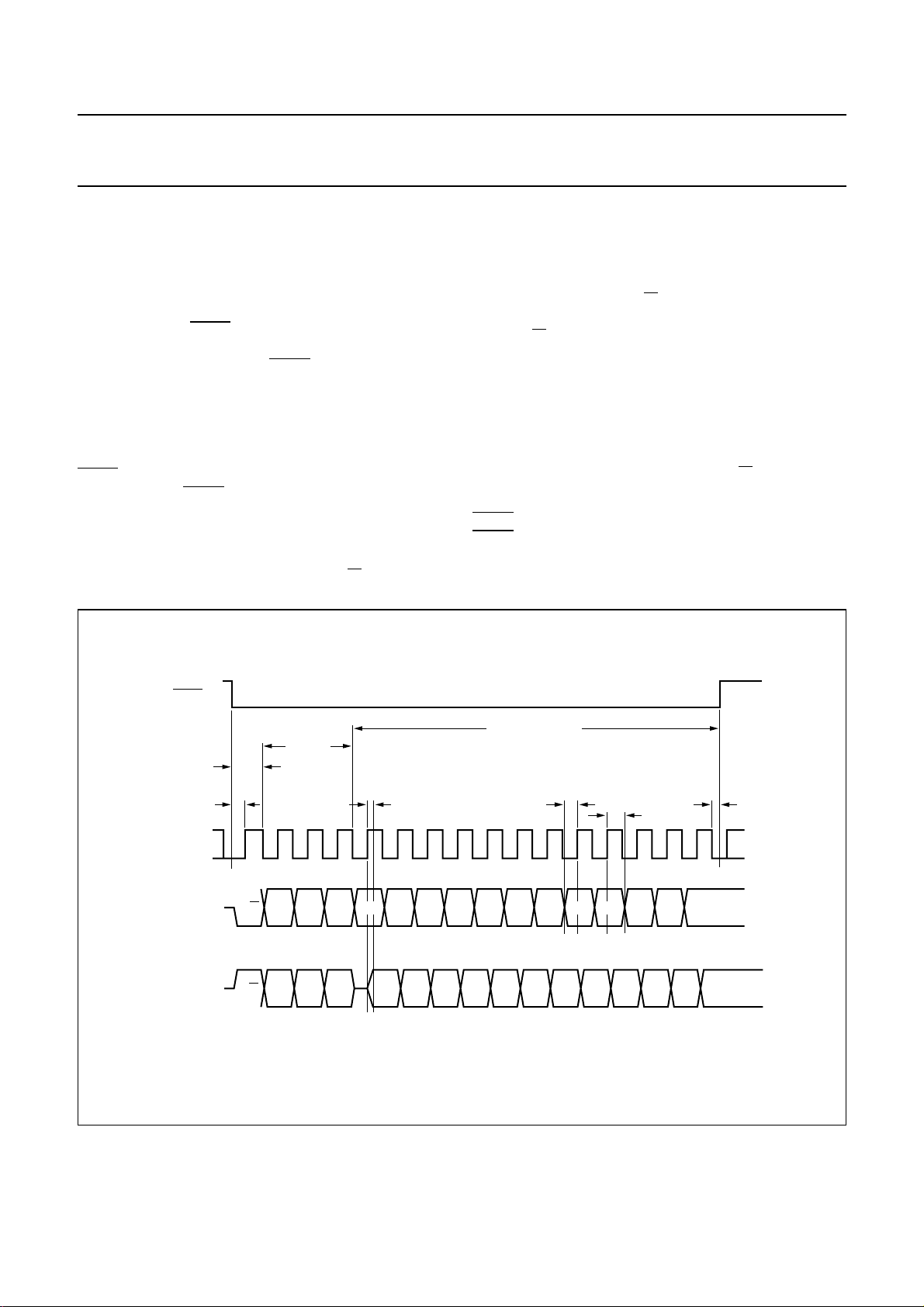
The serial interface is a 3-wire bidirectional port for writing
and reading data to and from the internal registers of the
OM5193H. Each read or write will be composed of 16 bits.
For data transfer
presented at the SDATA pin, and a serial clock is applied
to the SCLOCK pin. After the SDEN pin goes LOW, the
first 16 pulses applied to the SCLOCK pin shift the data
presented at the SDATA pin into an internal shift register
on the rising edge of each clock pulse. An internal counter
prevents more than 16 bits from being shifted into the
register. The data in the shift register is latched when
SDEN goes HIGH. If less than 16 clock pulses are
provided before SDEN goes HIGH, the data transfer is
aborted.
All transfers are shifted into the serial port with the MSB
first. The first 4 bits of the transfer contain address and
instruction information. The MSB is the R/W bit which
SDEN is brought LOW, serial data is
OM5193H
determines if the transfer is a read (logic 1) or a
write (logic 0).
The remaining 3 bits determine the internal register to be
accessed. The other 12 bits contain the programming
data. In the read mode (R/
the register contents of the selected address. In the write
mode (R/W = 0), the OM5193H loads the selected register
with the data presented on the SDATA pin. During sleep
mode, the serial port remains active and register
programmed data is retained.
SCLOCK is driven by the microcontroller. When the
microcontroller drives the SDATA line, the data is valid on
the rising edge of SCLOCK. When the OM5193H is driving
the SDATA line (in read mode after the R/W bit and 3 bits)
the data is valid on the falling edge of SCLOCK.
SDEN marks the end of the serial transfer. When the
SDEN pin goes HIGH, the shift register data is latched into
the addressed register of the OM5193H.
W = 1), the OM5193H outputs
handbook, full pagewidth
SDEN
SCLOCK
SDATA
Write to the OM5193H
SDATA
Write to, then read from the OM5193H
send/receive data
address
direction
325476981110 1312 14 1615 1
t
st
R/W
R/W
A1A2 D11A0 D9D10 D7D8 D5D6 D3D4 D2 D0D1
write registers read back data
A1A2 D11A0 D9D10 D7D8 D5D6 D3D4 D2 D0D1
t
ren
t
su
t
hd
t
ex
MGM977
Fig.6 Serial port timing information.
1998 Nov 02 13
Philips Semiconductors Product specification
Disk drive spindle and VCM with
OM5193H
servo controller
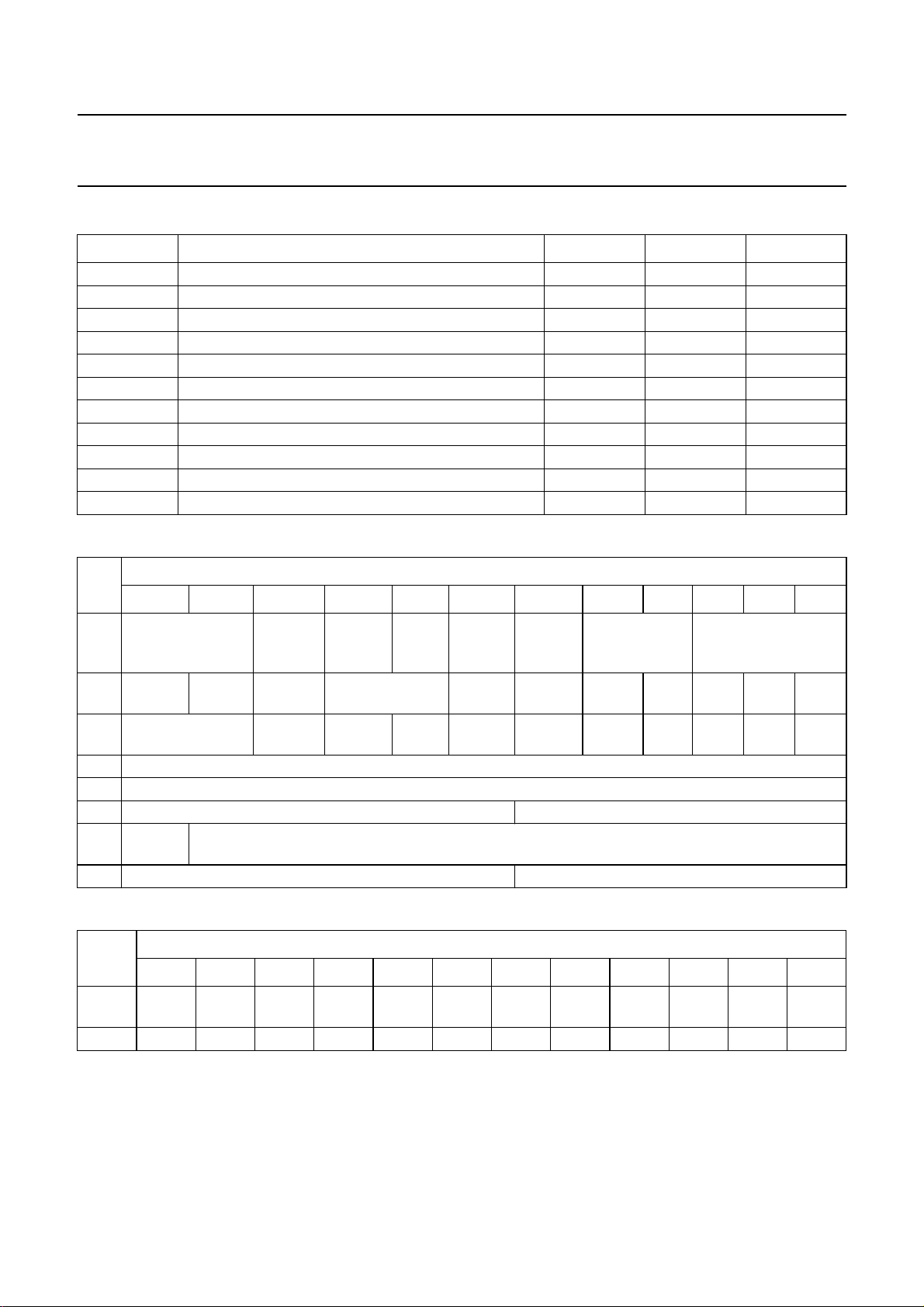
Table 1 Timing information for the serial interface
SYMBOL PARAMETER MIN. MAX. UNIT
f
clk
t
st
t
su
t
hd
t
rd
t
ren
t
rhd
t
rsu
t
exW
t
exR
T
bpa
Table 2 Writeable registers of the serial interface
REG
0 not used
1 reverse
break
2 not used
3 not used
4 not used
5 Watchdog Blank 1
6 high
Clock_N
7 Start-up Blank 2
clock frequency − 30 MHz
chip select to first active clock edge
1
⁄2T
clk
− ns
data to clock set-up time 12 − ns
clock to data hold time 12 − ns
time data line is driven after 5th negative clock − 5ns
time from positive clock for data line to be driven 0 − ns
receive data hold time 0 − ns
receive data set-up time 12 − ns
last active clock to chip select; inactive on write 0 − ns
last active clock to chip select; inactive on read 10 − ns
time between successive serial port accesses 5 − clock cycles
BITS
11 10 9 8 7 6 5 4 3210
auto
Conv.
select
range
Select
test
Mode_N
not used ADC MUX address
not used sleep_N spindiv manual
DAC
(7)
DAC
(6)
DAC
(5)
DAC
(4)
run/
comC comB comA
stop
DAC
(3)
DAC
(2)
DAC
(1)
not
used
opamp
Select_N
seek/
trackfw
DAC
(9)
increm.
Channel
DAC
(8)
Comdelim
DAC
(0)
Table 3 Readable registers of the serial interface
BITS
REG
11109876543210
0 ADC
status
ADC
(9)
ADC
(8)
ADC
(7)
ADC
(6)
ADC
(5)
ADC
(4)
ADC
(3)
ADC
(2)
ADC
(1)
1 Ccross Bcross Across
1998 Nov 02 14
ADC
(0)

Philips Semiconductors Product specification
Disk drive spindle and VCM with
OM5193H
servo controller
Table 4 Address of registers
R/W A2 A1 A0 REG. DESCRIPTION
00000ADC channel and programmable options
10000ADC status and value
00011commutation, sleep, and VCM switch controls
10011commutation state in manual mode
0010210-bit DAC
00113not used
01004not used
01015Blank 1 and Watchdog delays
01106commutation delay limit (11 bits), internal clock divider factor
01117Start-up and Blank 2 delays
8.2 Commutation and sleep mode
Spindle control and sleep mode are controlled by writing or
reading on register#1.
• Register#1 (0, 1 and 2) control the spindle
commutations in manual mode when run/stop, manual
and sleep bits are correctly set. The commutation
sequence is described in Section “Spindle driver” (see
also Table 16 and Fig.12).
• Register#1 (3) is the run/stop bit. After the power is
turned on and POR is HIGH, the motor will not start
spinning until register#1 (3) has been set to logic 1.
The motor stops spinning when this bit is set to logic 0.
• Register#1 (4) is the manual commutation mode bit.
When this bit is set to logic 1 and register#1 (3) set to
logic 1, the commutation logic in the OM5193H will be
disabled so that the spindle will not automatically go to
the next commutation.
When register#1 (3 and 4) are set to logic 1, the
microcontroller is expected to generate the different
commutation states for the motor. The OM5193H will
still provide the coil status which will be available by
reading register#1. The different waveforms are shown
in Section “Spindle driver” (see also Fig.12). Note that
depending on the coil status acquisition moment,
transient states (due to the flyback pulses) can be read.
When register#1 (4) is set to logic 0, the manual mode
is disabled and the OM5193H will automatically
commutate the motor each time a zero crossing is
detected. The time between the zero crossing and the
next commutation is half the time between the two
preceding zero crossings. This is explained in the
detailed description in Section “Commutation control”.
• Register#1 (5) is the spindiv bit. This bit together with
register#6 (11) enables the selection of a divider factor
for both converter clock and spindle clock. Clock
configurations are described in Section “Commutation
control” (see also Table 6).
• Register#1 (6) is the sleep mode bit. When it is set to
logic 0, the OM5193H will enter the low power mode.
Then the commutation control generates (101) output
codes on commutation signals to set spindle and VCM
head into sleep mode. This causes the OM5193H to go
into the brake-after-park mode. The only operating
circuits are the power monitor, the voltage reference
generator, the VCM precharge circuit and the serial
interface. The OM5193H is in sleep mode when
LOW.
When the power is first turned on, the POR signal goes
HIGH after the POR delay. The OM5193H is then
automatically set in sleep mode and thus in low power
consumption mode. The VCM DAC output is in
high-impedance mode, the spindle is in the brake mode
and the VCM is in the precharge mode. Only after POR
is HIGH and register#1 (6) is set to logic 1, OM5193H is
ready to be functional. When register#1 (6) goes HIGH,
the VCM DAC outputs the 2.5 V reference voltage.
• Register#1 (11) is dedicated to brake the spindle motor
without going in ‘brake-after-park’ mode.
The commutation sequence is shifted in order to
efficiently brake the motor. This brake, called reverse
brake, is activated when register#1 (11) bit is set to
logic 1. Note that there is no action on the VCM input
signal when the reverse brake is used. When this bit is
set to logic 0, the spindle motor starts again with normal
spindle commutations.
POR is
1998 Nov 02 15

Philips Semiconductors Product specification
Disk drive spindle and VCM with
OM5193H
servo controller
Reading register#1 will read the state of the 3 coils coming
from the spindle control block (ACROSS, BCROSS and
CCROSS). The 3 input lines will be in bits 0, 1, and 2.
The different waveforms are shown in Section “Spindle
Table 5 Writing register#1
BIT
0 0 comA drives COMA when in manual commutation
1 0 comB drives COMB when in manual commutation
2 0 comC drives COMC when in manual commutation
3 0 run/stop 0 = motor to brake-after-park mode
4 0 manual 0 = automatic commutation mode with run/stop = 1
5 0 spindiv 0 = the internal spindle clock frequency is controlled by register#6 (11)
6 0 sleep_N 0 = sleep mode: low power mode, serial interface active, power stages in
70− not used
80− not used
9 1 seek/trackfw 0 = VCMIN connected to SEEKSELECT
10 1 − not used
11 0 reverse break 1 = active brake control
DEFAULT
VALUE
NAME DESCRIPTION
1 = motor spinning; VCM active
1 = manual commutation mode with run/stop = 1
(bit highClock_N)
1 = an additional divider by 4 is added on the internal spindle clock
brake-after-park mode
1 = fully functional mode: sleep_N has higher priority than run/stop if both are
active
1 = VCMIN connected to TRACKFWSELECT
0 = normal commutations as defined by bits above
driver” (see also Fig.12). Note that depending on the coil
status acquisition moment, transient states (due to the
flyback pulses) can be read.
8.3 Commutation control
The commutation logic block generates the six different
states to rotate the spindle motor. The spindle driver block
provides the BEMF zero crossing information.
The commutation block interprets the zero crossing
information and determines the commutation delay time
and the next coil state. The commutation block must take
into account the following situations:
• Start-up
• No start
• Reverse rotating
• Run
• Manual commutation.
1998 Nov 02 16
The commutation logic keeps the motor spinning by
commutating the motor after each detected zero crossing.
It measures the time between two successive BEMF zero
crossings and then determines the next commutation.
The delay (commutation delay) between a zero crossing
and the next commutation is half the time between the two
preceding zero crossings. The commutation delay
(Comdelim) can be limited to guarantee a faster lock after
the motor has gone out of lock. A maximum commutation
delay can be set via the serial port. The time is a function
of both the external clock frequency, the individual register
prescalers and the time programmed into the registers.
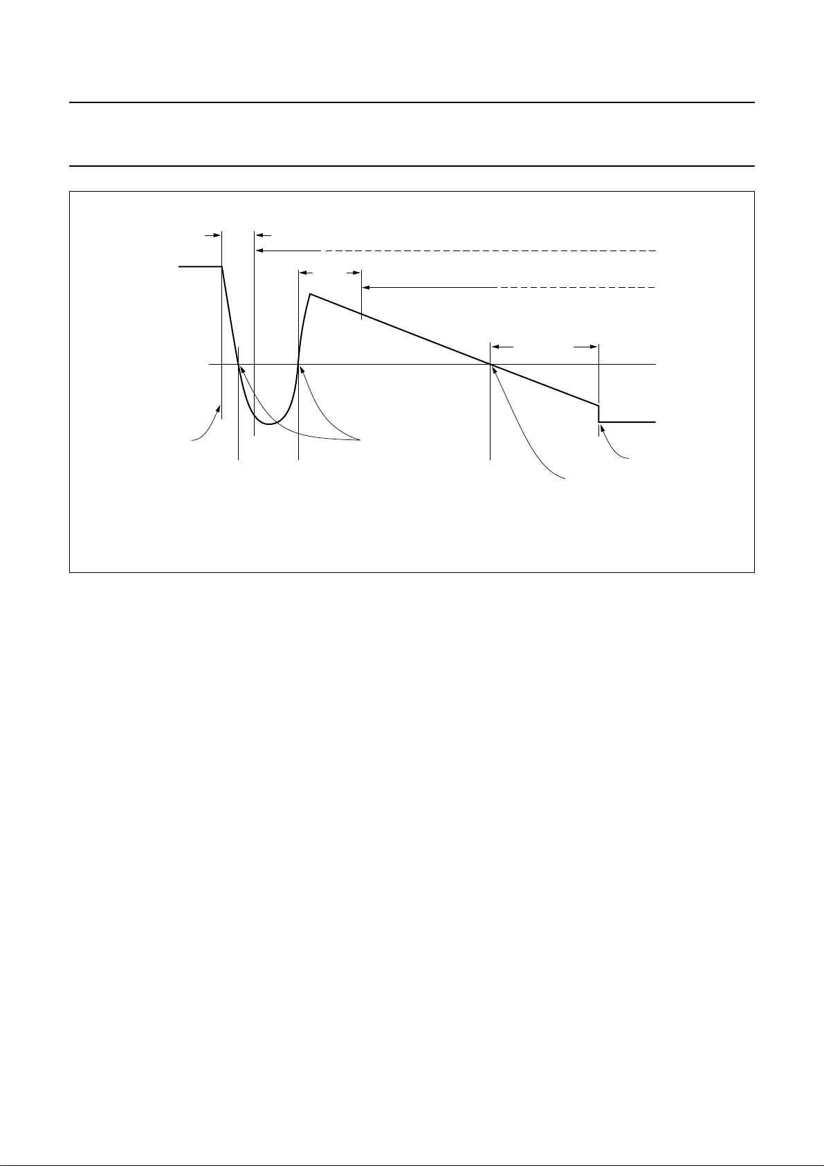
Figure 7 shows a typical motor commutation timing
diagram.
Philips Semiconductors Product specification
Disk drive spindle and VCM with
servo controller
handbook, full pagewidth
Blank 1
centre tap
commutation
Zc
1
flyback pulse
Watchdog
Zc
2
Blank 2
Start-up
false zero crossings
Zc
3
Commutation
delay
OM5193H
commutation
true zero crossing
MGM978
Fig.7 A typical motor commutation diagram.
• Blank 1
After a commutation occurs, the leading edge of the
flyback pulse has a zero crossing (Zc1). Blank 1 timer is
used to ignore this zero crossing by masking it while the
timer initialized at Blank 1 value is counting. The state
associated to Blank 1 down-counter will end when the
counter reaches the zero value.
• Blank 2
The Blank 2 timer starts counting as soon as the second
zero crossing occurs (Zc2). After the second flyback
pulse zero crossing, all extra zero crossings are ignored
during the Blank 2 time. This allows the ringing of the
coil voltage without causing a commutation advance.
The state associated to Blank 2 down-counter will end
when the counter reaches the zero value.
• Watchdog
The Watchdog timer makes sure the motor is running in
forward direction. If the motor is rotating in reverse
direction, the BEMF voltage is inverted and the second
crossing of the flyback pulse (Zc2) will not occur until the
true BEMF zero crossing is detected. Therefore, if the
Watchdog timer expires before a zero crossing occurs,
the motor is assumed to be rotating backwards.
The commutation is advanced by one step to correct
this condition. The Watchdog time must be set to a value
that is greater than the flyback pulse duration, measured
when the spindle motor stands still.
The state associated to the Watchdog timer will start
when the one associated to Blank 1 timer is finished and
will end when Zc2 occurs or when the Watchdog counter
expires.
• Start-up
If the motor is not spinning, the BEMF zero crossings will
not occur. The Start-up timer detects this if it expires
before the true zero crossing (Zc3) has occurred. It will
advance the commutation by one step if this happens.
The state associated to Start-up timer will start when the
one associated to Blank 2 timer is finished and will end
when Zc3 occurs or when Start-up expires.
• Comdelim
The timer associated to Comdelim value allows to
control the maximum commutation delay (between zero
crossing and next commutation). When the true zero
crossing is detected (Zc3), the timer will count until it
expires and then will commutate the motor to the next
step. This commutation delay time is equal to half the
measured value between 2 zero crossings.
The Comdelim value should be set to the maximum
allowable delay value. If ∆Zc
is lower than the
meas
programmed Comdelim value, the next timer value will
be ∆Zc
divided by 2. If ∆Zc
meas
is higher than the
meas
programmed Comdelim value, the next timer value will
be the programmed Comdelim value divided by 2.
1998 Nov 02 17
 Loading...