

Philips OM4085T Datasheet

INTEGRATED CIRCUITS
DATA SH EET
OM4085
Universal LCD driver for low
multiplex rates
Product specification
Supersedes data of 1996 Nov 14
File under Integrated Circuits, IC12
1997 Feb 25

Philips Semiconductors Product specification
Universal LCD driver for low multiplex
rates
FEATURES
• Single-chip LCD controller/driver
• Selectable backplane drive configuration: static
or 2, 3 or 4 backplane multiplexing
• Selectable display bias configuration: static,1⁄2or1⁄
• Internal LCD bias generation with voltage-follower
buffers
• 24 segment drives: up to twelve 8-segment numeric
characters; up to six 15-segment alphanumeric
characters; or any graphics of up to 96 elements
• 24 × 4-bit RAM for display data storage
• Auto-incremented display data loading across device
subaddress boundaries
• Display memory bank switching in static and duplex
drive modes
• Versatile blinking modes
• LCD and logic supplies may be separated
• 2.0 to 6 V power supply range
• Low power consumption
• Power saving mode for extremely low power
consumption in battery-operated and telephone
applications
2
C-bus interface
• I
• TTL/CMOS compatible
• Compatible with any 4-bit, 8-bit or 16-bit
microprocessors/microcontrollers
• May be cascaded for large LCD applications
(up to 1536 segments possible)
• Cascadable with the 40 segment LCD driver PCF8576C
• Optimized pinning for single plane wiring in both single
and multiple OM4085 applications
• Space-saving 40 lead plasticvery small outline package
(VSO40; SOT158-1)
• No external components required (even in multiple
device applications)
• Manufactured in silicon gate CMOS process.
3
OM4085
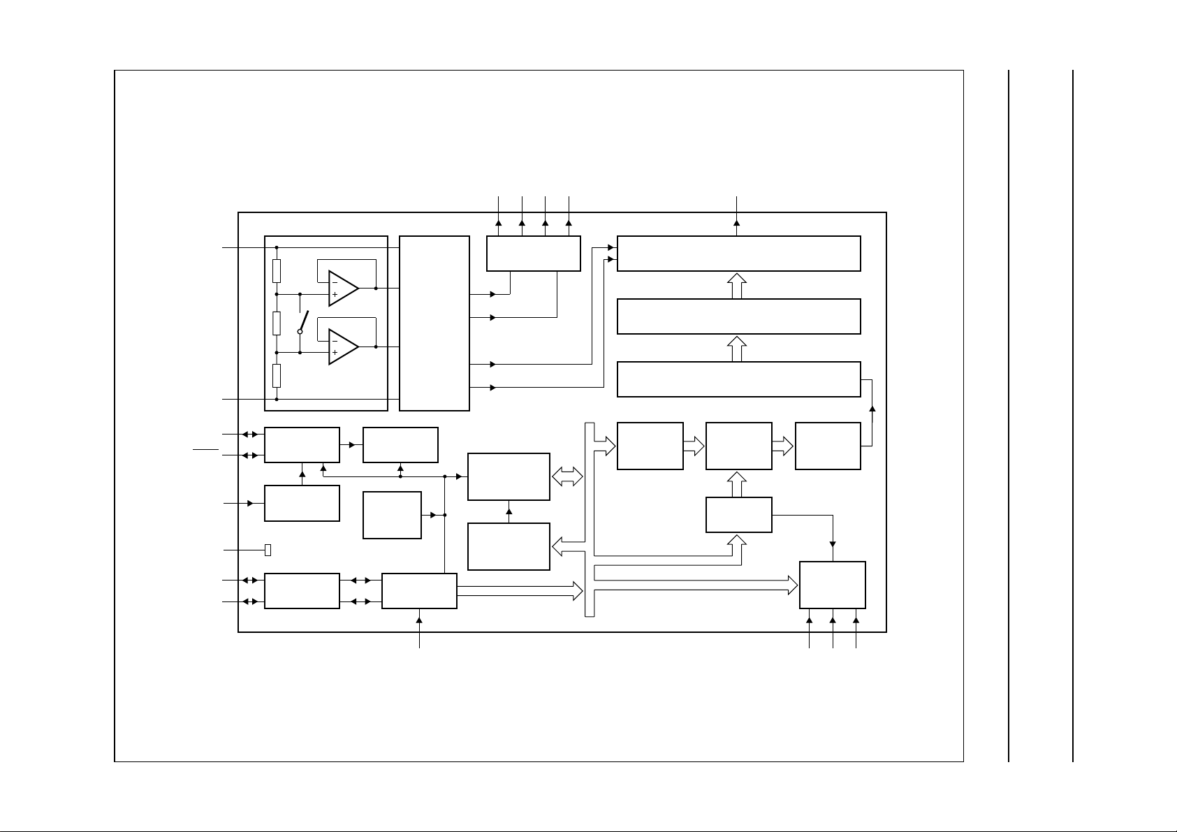
GENERAL DESCRIPTION
The OM4085 is a peripheral device which interfaces to
almost any Liquid Crystal Display (LCD) having low
multiplex rates. It generates the drive signals for any static
or multiplexed LCD containing up to four backplanes and
up to 24 segments and can easily be cascaded for larger
LCD applications. The OM4085 is compatible with most
microprocessors/microcontrollers and communicates via a
two-line bidirectional I
are minimized by a display RAM with auto-incremented
addressing, by hardware subaddressing and by display
memory switching (static and duplex drive modes).
2
C-bus. Communication overheads
ORDERING INFORMATION
TYPE NUMBER
NAME DESCRIPTION VERSION
OM4085T VSO40 plastic very small outline package; 40 leads SOT158-1
1997 Feb 25 2
PACKAGE
This text is here in white to force landscape pages to be rotated correctly when browsing through the pdf in the Acrobat reader.This text is here in
_white to force landscape pages to be rotated correctly when browsing through the pdf in the Acrobat reader.This text is here inThis text is here in
white to force landscape pages to be rotated correctly when browsing through the pdf in the Acrobat reader. white to force landscape pages to be ...
1997 Feb 25 3
handbook, full pagewidth
BLOCK DIAGRAM
Universal LCD driver for low multiplex
rates
Philips Semiconductors Product specification
V
DD
V
LCD
CLK
SYNC
OSC
V
SS
SCL
SDA
5
12
4
3
6
11
2
1
R
R
LCD BIAS
R
GENERATOR
TIMING BLINKER
OSCILLATOR
INPUT
FILTERS
POWER-
RESET
LCD
VOLTAGE
SELECTOR
ON
2
I C-BUS
CONTROLLER
10
BP014BP215BP116BP3
13
BACKPLANE
OUTPUTS
OM4085
DISPLAY
CONTROLLER
COMMAND
DECODER
INPUT
BANK
SELECTOR
S0 to S23
17 to 40
DISPLAY SEGMENT OUTPUTS
DISPLAY LATCH
SHIFT REGISTER
DISPLAY
RAM
24 × 4 BITS
DATA
POINTER
OUTPUT
BANK
SELECTOR
SUBADDRESS
COUNTER
9
SA0
Fig.1 Block diagram.
A07A18A2
MGD866
OM4085
Philips Semiconductors Product specification
Universal LCD driver for low multiplex
rates
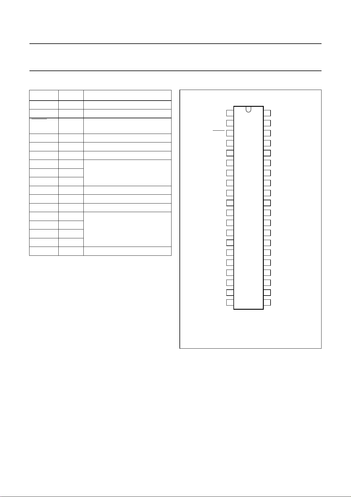
PINNING
SYMBOL PIN DESCRIPTION
2
SDA 1 I
SCL 2 I
SYNC 3 cascade synchronization
CLK 4 external clock input/output
V
DD
5 positive supply voltage
OSC 6 oscillator input
A0 7
A2 9
SA0 10 I
V
V
SS
LCD
11 logic ground
12 LCD supply voltage
BP0 13
BP2 14
BP1 15
BP3 16
S0 to S23 17 to 40 LCD segment outputs
C-bus data input/output
2
C-bus clock input/output
input/output
2
I
C-bus subaddress inputsA1 8
2
C-bus slave address bit 0 input
LCD backplane outputs
handbook, halfpage
SDA
SCL
SYNC
CLK
V
DD
OSC
A0
A1
A2
SA0
V
SS
V
LCD
BP0
BP2
BP1
BP3
S0
S1
S2
S3
1
2
3
4
5
6
7
8
9
10
11
12
13
14
15
16
17
18
19
20
OM4085
MGD865
OM4085
40
S23
39
S22
38
S21
37
S20
36
S19
35
S18
34
S17
33
S16
32
S15
31
S14
30
S13
29
S12
28
S11
27
S10
26
S9
25
S8
24
S7
23
S6
22
S5
21
S4
1997 Feb 25 4
Fig.2 Pin configuration.
Philips Semiconductors Product specification
Universal LCD driver for low multiplex
rates
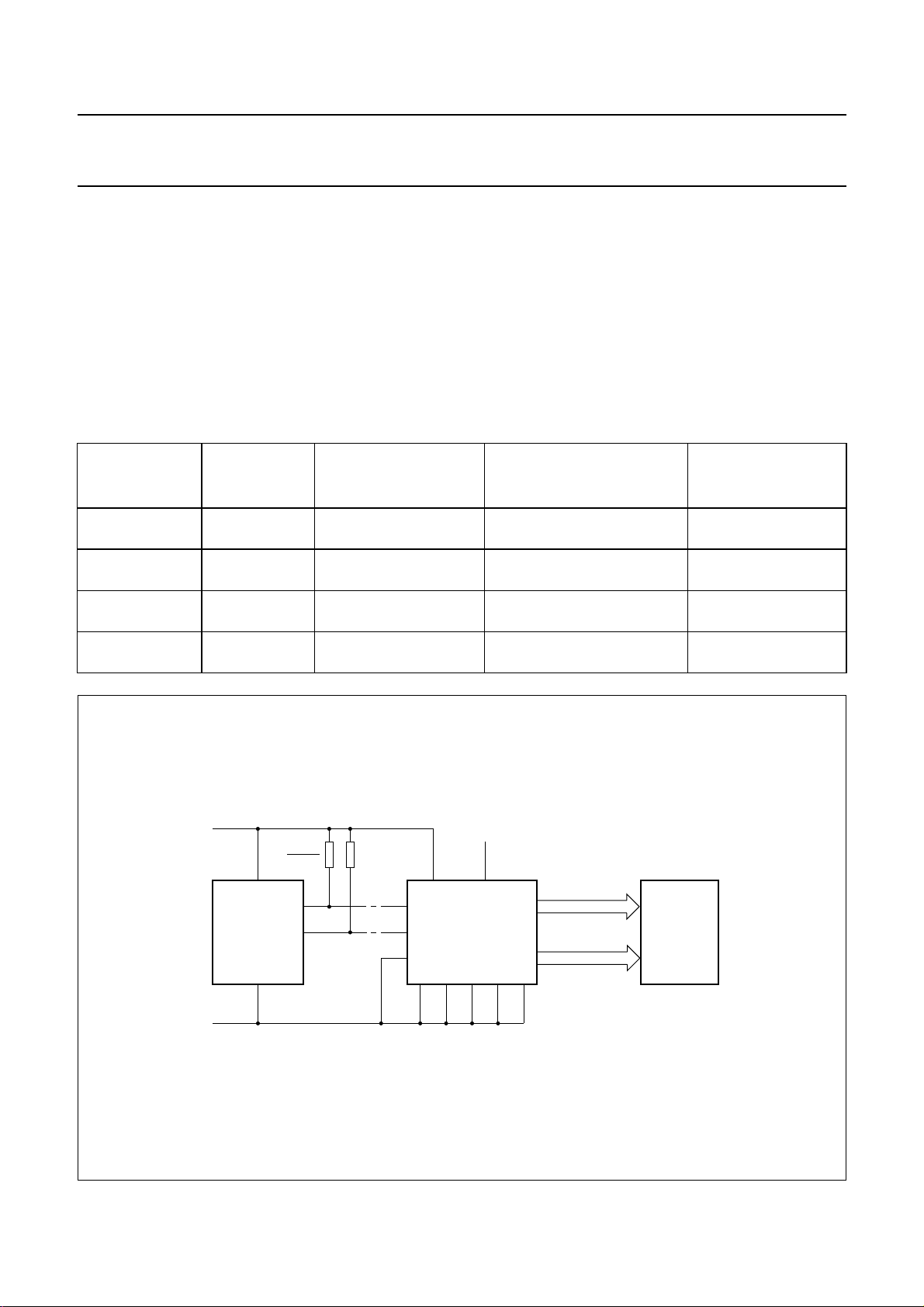
FUNCTIONAL DESCRIPTION
The OM4085 is a versatile peripheral device designed to
interface any microprocessor to a wide variety of LCDs.
It can directly drive any static or multiplexed LCD
containing up to 4 backplanes and up to 24 segments.
The display configurations possible with the OM4085
depend on the number of active backplane outputs
required; a selection of display configurations is given in
Table 1.
Table 1 Selection of display configurations
ACTIVE
BACKPLANE
OUTPUTS
4 96 12 digits + 12 indicator
3 72 9 digits + 9 indicator
2 48 6 digits + 6 indicator
1 24 3 digits + 3 indicator
NUMBER OF
SEGMENTS
7-SEGMENT NUMERIC
symbols
symbols
symbols
symbols
OM4085
All of the display configurations given in Table 1 can be
implemented in the typical system shown in Fig.3.
The host microprocessor/microcontroller maintains the
two-line I
OM4085. The internal oscillator is selected by tying OSC
(pin 6) to VSS. The appropriate biasing voltages for the
multiplexed LCD waveforms are generated internally.
The only other connections required to complete the
system are to the power supplies (VDD, VSSand V
to the LCD panel chosen for the application.
2
C-bus communication channel with the
14-SEGMENT
ALPHANUMERIC
6 characters + 12 indicator
symbols
4 characters + 16 indicator
symbols
3 characters + 6 indicator
symbols
1 character + 10 indicator
symbols
DOT MATRIX
96 dots (4 × 24)
72 dots (3 × 24)
48 dots (2 × 24)
24 dots
LCD
) and
handbook, full pagewidth
V
DD
V
SS
R ≤
2 C
HOST
MICRO-
PROCESSOR/
MICRO-
CONTROLLER
t
rise
bus
SDA
SCL
OSC
V
DD
512
1 17 to 40
OM4085
2
6
78
A0 A1 A2 SA0
Fig.3 Typical system configuration.
1997 Feb 25 5
V
LCD
13 to 16
91011
V
24 segment drives
4 backplanes
SS
LCD PANEL
(up to 96
elements)
MBH951
Philips Semiconductors Product specification
Universal LCD driver for low multiplex
rates
Power-on reset
At power-on the OM4085 resets to a defined starting
condition as follows:
1. All backplane outputs are set to V
2. All segment outputs are set to V
3. The drive mode ‘1 : 4 multiplex with1⁄3bias’ is selected
4. Blinking is switched off
5. Input and output bank selectors are reset (as defined
in Table 5)
6. The I2C-bus interface is initialized
7. The data pointer and the subaddress counter are
cleared.
2
Data transfers on the I
C-bus should be avoided for 1 ms
following power-on to allow completion of the reset action.
LCD bias generator
The full-scale LCD voltage (V
VDD− V
. The LCD voltage may be temperature
LCD
op
compensated externally through the V
Fractional LCD biasing voltages are obtained from an
internal voltage divider of three series resistors connected
between VDD and V
. The centre resistor can be
LCD
switched out of circuit to provide a1⁄2bias voltage level for
the 1 : 2 multiplex configuration.
DD
DD
) is obtained from
supply to pin 12.
LCD
OM4085
LCD voltage selector
The LCD voltage selector coordinates the multiplexing of
the LCD according to the selected LCD drive
configuration. The operation of the voltage selector is
controlled by MODE SET commands from the command
decoder. The biasing configurations that apply to the
preferred modes of operation, together with the biasing
− V
characteristics as functions of V
op=VDD
resulting discrimination ratios (D), are given in Table 2.
A practical value of V
is determined by equating V
op
with a defined LCD threshold voltage (Vth), typically when
the LCD exhibits approximately 10% contrast. In the static
drive mode a suitable choice is V
ratios of 1 : 3 and 1 : 4 with
≥ 3Vth. Multiplex drive
op
1
⁄2bias are possible but the
discrimination and hence the contrast ratios are smaller
( for 1 : 3 multiplex or for
3 1.732=
21 3⁄ 1.528=
1 : 4 multiplex). The advantage of these modes is a
reduction of the LCD full scale voltage V
6V
1
⁄2bias):
op(mrs)
1
⁄2bias):
off rms()
2.449V
==
op
=3V
off rms()
2.309V
off(rms)
1 : 3 multiplex (
V
op
1 : 4 multiplex (
Vop343⁄ V
==
These compare with V
op
off rms()
when1⁄3bias is used.
and the
LCD
off(rms)
as follows:
Table 2 Preferred LCD drive modes: summary of characteristics
LCD DRIVE MODE
LCD BIAS
CONFIGURATION
V
off rms()
----------------------V
op
V
on rms()
---------------------- V
op
D
=
Static (1 BP) static (2 levels) 0 1 ∞
1 : 2 MUX (2 BP)
1 : 2 MUX (2 BP)
1 : 3 MUX (3 BP)
1 : 4 MUX (4 BP)
1
⁄2(3 levels)
1
⁄3(4 levels)
1
⁄3(4 levels)
1
⁄3(4 levels)
2 4 0.354=⁄
1
⁄3= 0.333
1
⁄3= 0.333
1
⁄3= 0.333
10 4⁄ 0.791=
53⁄ 0.745=
52.236=
52.236=
33 9⁄ 0.638= 33 3⁄ 1.915=
33⁄ 0.577= 31.732=
1997 Feb 25 6
V
on rms()
----------------------V
off rms()
Philips Semiconductors Product specification
Universal LCD driver for low multiplex
OM4085
rates
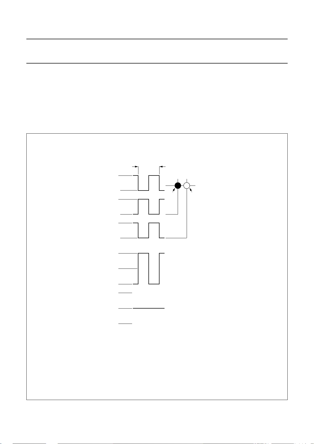
LCD drive mode waveforms
The static LCD drive mode is used when a single backplane is provided in the LCD. Backplane and segment drive
waveforms for this mode are shown in Fig.4.
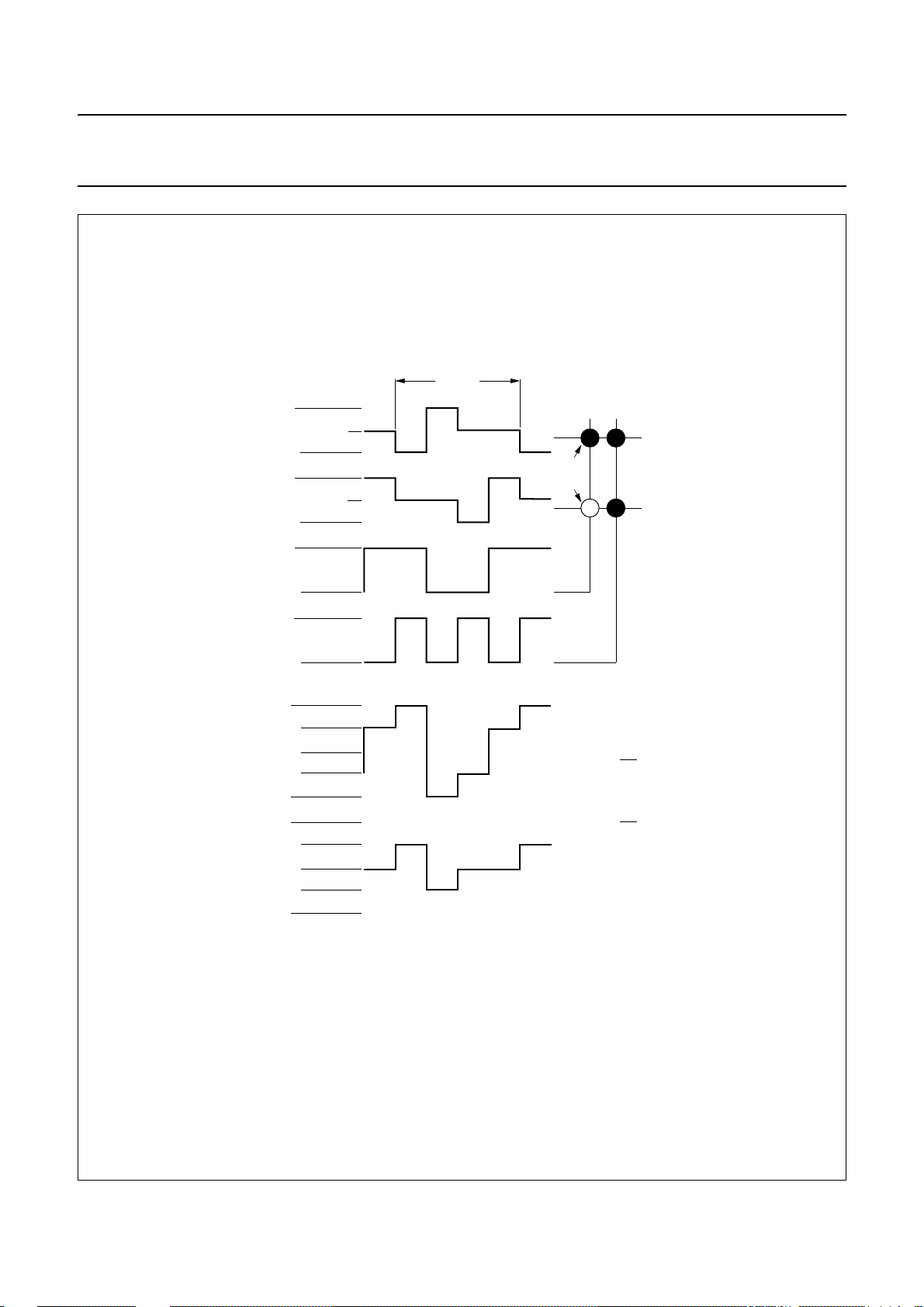
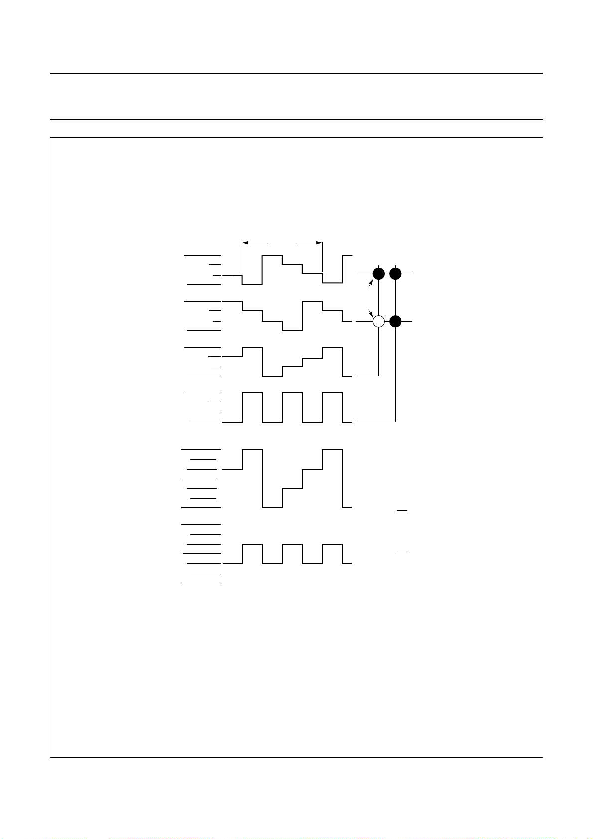
When two backplanes are provided in the LCD the 1 : 2 multiplex drive mode applies. The OM4085 allows use of
1
⁄2or1⁄3bias in this mode as shown in Figs 5 and 6.
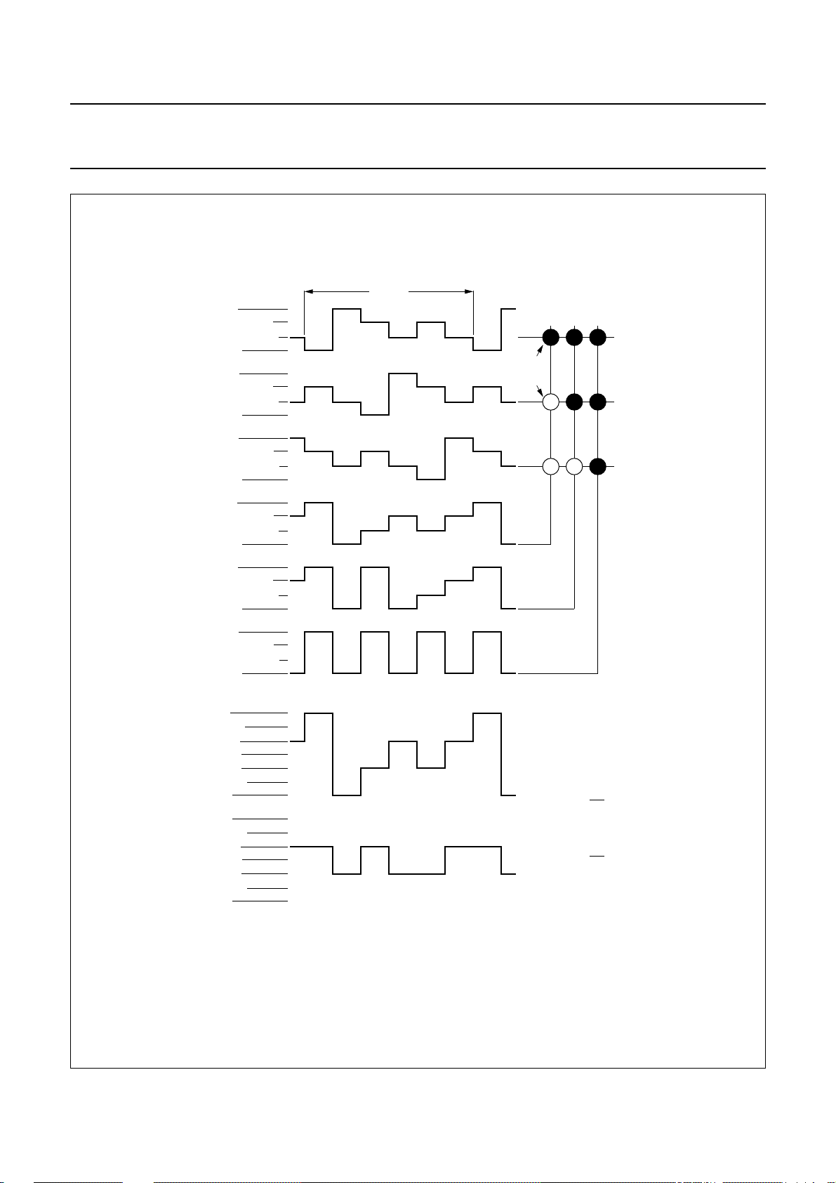
The backplane and segment drive waveforms for the 1 : 3 multiplex drive mode (three LCD backplanes) and for the 1 : 4
multiplex drive mode (four LCD backplanes) are shown in Figs 7 and 8 respectively.
T
handbook, full pagewidth
S
BP0
S
n + 1
V
DD
V
LCD
V
DD
n
V
LCD
V
DD
V
LCD
(a) waveforms at driver
frame
LCD segments
state 1
(on)
state 2
(off)
V
op
state 1
state 2 0
−V
−V
0
op
V
op
op
(b) resultant waveforms
at LCD segment
At any instant (t):
V
(t) = V
state 1
V
= V
on(rms)
V
(t) = V
state 2
V
= 0 V
off(rms)
Fig.4 Static drive mode waveforms: Vop=VDD− V
(t) − V
S
n
op
S
n + 1
(t) − V
LCD
BP0
MGG392
.
(t)
BP0
(t)
1997 Feb 25 7
Philips Semiconductors Product specification
Universal LCD driver for low multiplex
rates
handbook, full pagewidth
V
DD
(V
+ V
BP0
BP1
S
n
S
n + 1
state 1
DD
V
LCD
V
DD
(V
DD
V
LCD
V
DD
V
LCD
V
DD
V
LCD
V
op
Vop/2
−Vop/2
−V
op
V
op
Vop/2
)/2
LCD
+ V
)/2
LCD
(a) waveforms at driver
0
T
frame
LCD segments
state 1
state 2
At any instant (t):
V
(t) = V
state 1
V
=
on(rms)
V
(t) = V
state 2
V
=
off(rms)
(t) − V
S
n
V
op
√10 = 0.791V
4
(t) − V
S
n
V
op
√2 = 0.354V
4
BP0
BP1
OM4085
(t)
op
(t)
op
−Vop/2
−V
op
0
(b) resultant waveforms
at LCD segment
state 2
Fig.5 Waveforms for 1 : 2 multiplex drive mode with1⁄2bias: Vop=VDD− V
1997 Feb 25 8
MGG394
LCD
.
Philips Semiconductors Product specification
Universal LCD driver for low multiplex
rates
andbook, full pagewidth
BP0
BP1
S
n + 1
state 1 0
state 2 0
V
DD
V
− Vop/3
DD
V
− 2Vop/3
DD
V
LCD
V
DD
V
− Vop/3
DD
V
− 2Vop/3
DD
V
LCD
V
DD
V
− Vop/3
S
DD
n
V
− 2Vop/3
DD
V
LCD
V
DD
V
− Vop/3
DD
V
− 2Vop/3
DD
V
LCD
V
op
2Vop/3
Vop/3
−Vop/3
−2Vop/3
−V
op
V
op
2Vop/3
Vop/3
−Vop/3
−2Vop/3
−V
op
(a) waveforms at driver
(b) resultant waveforms
at LCD segment
T
frame
LCD segments
state 1
state 2
At any instant (t):
V
(t) = V
state 1
V
on(rms)
V
state 2
V
off(rms)
V
=
(t) = V
V
=
(t) − V
S
n
op
√5 = 0.745V
3
(t) − V
S
n
op
= 0.333V
3
BP0
BP1
MGG393
OM4085
(t)
op
(t)
op
Fig.6 Waveforms for 1 : 2 multiplex drive mode with1⁄3bias: Vop=VDD− V
1997 Feb 25 9
LCD
.
Philips Semiconductors Product specification
Universal LCD driver for low multiplex
rates
handbook, full pagewidth
V
DD
V
BP0
BP1
BP2
S
S
n + 1
S
n + 2
state 1 0
state 2 0
DD
V
DD
V
LCD
V
DD
V
DD
V
DD
V
LCD
V
DD
V
DD
V
DD
V
LCD
V
DD
V
DD
n
V
DD
V
LCD
V
DD
V
DD
V
DD
V
LCD
V
DD
V
DD
V
DD
V
LCD
V
op
2Vop/3
Vop/3
−Vop/3
−2Vop/3
−V
op
V
op
2Vop/3
Vop/3
−Vop/3
−2Vop/3
−V
op
− Vop/3
− 2Vop/3
− Vop/3
− 2Vop/3
− Vop/3
− 2Vop/3
− Vop/3
− 2Vop/3
− Vop/3
− 2Vop/3
− Vop/3
− 2Vop/3
T
(a) waveforms at driver
(b) resultant waveforms
at LCD segment
frame
LCD segments
state 1
state 2
At any instant (t):
V
state 1
V
on(rms)
V
state 2
V
off(rms)
(t) = V
V
=
(t) = V
=
(t) − V
S
n
op
√33 = 0.638V
9
(t) − V
S
n
V
op
= 0.333V
3
BP0
BP1
MGG395
OM4085
(t)
op
(t)
op
Fig.7 Waveforms for 1 : 3 multiplex drive mode: Vop=VDD− V
1997 Feb 25 10
LCD
.
Philips Semiconductors Product specification
Universal LCD driver for low multiplex
rates
handbook, full pagewidth
V
DD
V
− Vop/3
BP0
BP1
BP2
BP3
S
n
S
n + 1
Sn + 2
S
n + 3
state 1 0
state 2 0
DD
V
DD
V
LCD
V
DD
V
DD
V
DD
V
LCD
V
DD
V
DD
V
DD
V
LCD
V
DD
V
DD
V
DD
V
LCD
V
DD
V
DD
V
DD
V
LCD
V
DD
V
DD
V
DD
V
LCD
V
DD
V
DD
V
DD
V
LCD
V
DD
V
DD
V
DD
V
LCD
V
op
2Vop/3
Vop/3
−Vop/3
−2Vop/3
−V
op
V
op
2Vop/3
Vop/3
−Vop/3
−2Vop/3
−V
op
− 2Vop/3
− Vop/3
− 2Vop/3
− Vop/3
− 2Vop/3
− Vop/3
− 2Vop/3
− Vop/3
− 2Vop/3
− Vop/3
− 2Vop/3
− Vop/3
− 2Vop/3
− Vop/3
− 2Vop/3
(a) waveforms at driver
(b) resultant waveforms
at LCD segment
T
frame
LCD segments
state 1
state 2
At any instant (t):
V
state 1
V
on(rms)
V
state 2
V
off(rms)
(t) = V
V
=
(t) = V
V
=
(t) − V
S
n
op
√3 = 0.577V
3
(t) − V
S
n
op
= 0.333V
3
MGG396
OM4085
(t)
BP0
op
(t)
BP1
op
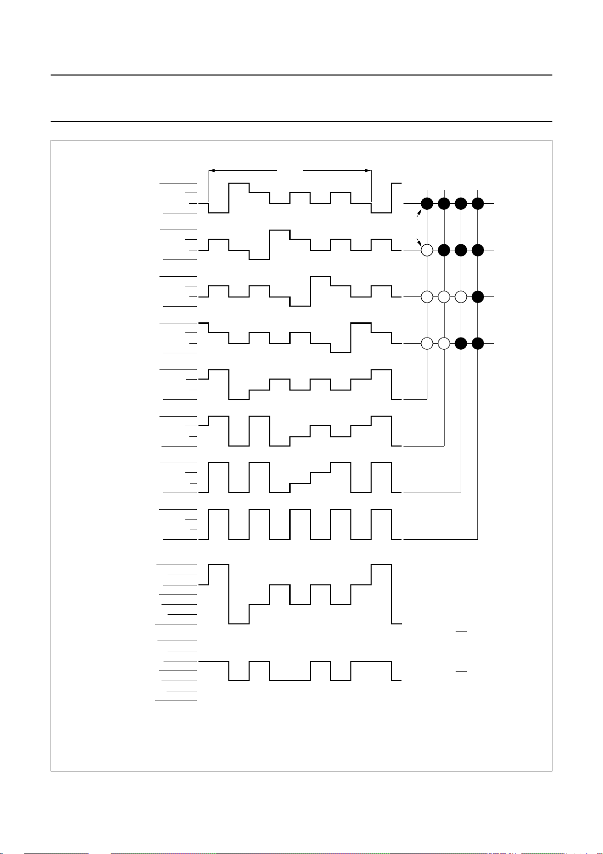
Fig.8 Waveforms for 1 : 4 multiplex drive mode: Vop=VDD− V
1997 Feb 25 11
LCD.
 Loading...