

Philips OM4068P-F1 Datasheet

DATA SH EET
Product specification
File under Integrated Circuits, IC12
1998 Jun 18
INTEGRATED CIRCUITS
OM4068
LCD driver for low multiplex rates
1998 Jun 18 2
Philips Semiconductors Product specification
LCD driver for low multiplex rates
OM4068
FEATURES
• Single-chip LCD controller/driver
• Static/duplex/triplex drive modes with up to
32/64/96 LCD segments drive capability per device
• Selectable backplane drive configuration: static or
2 or 3 backplane multiplexing
• Selectable display bias configuration drive: static,1⁄2 or
1
⁄
3
• 32 segment drivers
• Serial data input (word length 32 to 96 bits)
• On-chip generation of intermediate LCD bias voltages
• 2 MHz fast serial bus interface
• CMOS compatible
• Compatible with any 4-bit, 8-bit or 16-bit
microprocessors/microcontrollers
• May be cascaded for large LCD applications
• Logic supply voltage range (V
DD
− VSS) of 2.5 to 5.5 V
• Display supply voltage range (V
LCD
− VSS) of
3.5 to 6.5 V
• Low power consumption, suitable for battery operated
systems
• No external components needed by the oscillator
• Manufactured in silicon gate CMOS process.
APPLICATIONS
• Telecom equipment
• Portable instruments
• Alarm systems
• Automotive equipment.
GENERAL DESCRIPTION
The OM4068 is a low-power CMOS LCD driver, designed
to drive Liquid Crystal Displays (LCDs) with low multiplex
rates. It generates the drive signals for any static or
multiplexed LCD containing up to three backplanes and up
to 32 segment lines and can be easily cascaded for larger
LCD applications. All necessary functions for the display
are provided in a single chip, including on-chip generation
of LCD bias voltages, resulting in a minimum of external
components and lower power consumption. A 3-line bus
structure enables serial data transfer with most
microprocessors/microcontrollers. All inputs are CMOS
compatible.
ORDERING INFORMATION
Notes
1. Gull Wing package.
2. For details see Chapter “Bonding pad locations”.
TYPE NUMBER
PACKAGE
NAME DESCRIPTION VERSION
OM4068H
(1)
QFP44 plastic quad flat package; 44 leads (lead length 1.3 mm);
body 10 × 10 × 1.75 mm
SOT307-2
OM4068P DIP40 plastic dual in-line package; 40 leads (600 mil) SOT129-1
OM4068U/5
(2)
die unsawn wafer −
OM4068U tray chip in tray −
1998 Jun 18 3
Philips Semiconductors Product specification
LCD driver for low multiplex rates
OM4068
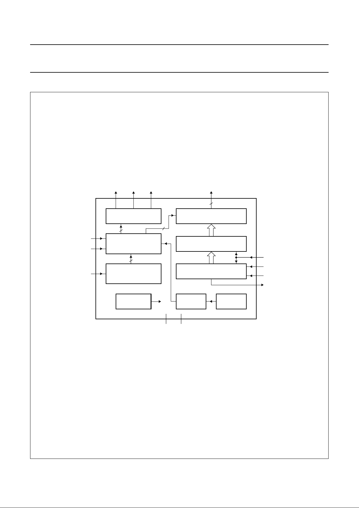
BLOCK DIAGRAM
Fig.1 Block diagram.
handbook, full pagewidth
MBK817
BACKPLANE OUTPUTS
OM4068
LCD VOLTAGE
SELECTOR
(CONTROL LOGIC)
BP2BP1 BP3 SEG1 to SEG32
(1)
DISPLAY SEGMENT OUTPUTS
TIMING
GENERATOR
VSSV
DD
DISPLAY LATCH
OSCILLATOR
BIAS
VOLTAGE
GENERATOR
POWER-ON
RESET
4
4
M0
M1
V
LCD
32
4
SHIFT REGISTER
SCE
SCLK
SDIN
SDOUT
(1) SEG1, SEG6, SEG15 and SEG25 are not available in DIP40 package.
1998 Jun 18 4
Philips Semiconductors Product specification
LCD driver for low multiplex rates
OM4068
PINNING
See notes 1 to 8.
SYMBOL
PIN
DESCRIPTION
QFP44 DIP40
V
LCD
4 19 LCD supply voltage
V
DD
5 20 positive supply voltage
V
SS
6 21 ground
M0 7 22 drive mode select input 0
M1 8 23 drive mode select input 1
SDIN 9 24 serial bus data input
SCLK 10 25 serial bus clock input
SCE 11 26 serial bus clock enable
SDOUT 12 27 serial bus data output
BP1 13 28 LCD backplane driver output 1
BP2 14 29 LCD backplane driver output 2
BP3 15 30 LCD backplane driver output 3
SEG1 16 − LCD segment driver output 1
SEG2 17 31 LCD segment driver output 2
SEG3 18 32 LCD segment driver output 3
SEG4 19 33 LCD segment driver output 4
SEG5 20 34 LCD segment driver output 5
SEG6 21 − LCD segment driver output 6
SEG7 22 35 LCD segment driver output 7
SEG8 23 36 LCD segment driver output 8
SEG9 24 37 LCD segment driver output 9
SEG10 25 38 LCD segment driver output 10
SEG11 26 39 LCD segment driver output 11
SEG12 27 40 LCD segment driver output 12
SEG13 28 1 LCD segment driver output 13
SEG14 29 2 LCD segment driver output 14
SEG15 30 − LCD segment driver output 15
SEG16 31 3 LCD segment driver output 16
SEG17 32 4 LCD segment driver output 17
SEG18 33 5 LCD segment driver output 18
SEG19 34 6 LCD segment driver output 19
SEG20 35 7 LCD segment driver output 20
SEG21 36 8 LCD segment driver output 21
SEG22 37 9 LCD segment driver output 22
SEG23 38 10 LCD segment driver output 23
SEG24 39 11 LCD segment driver output 24
SEG25 40 − LCD segment driver output 25
SEG26 41 12 LCD segment driver output 26
1998 Jun 18 5
Philips Semiconductors Product specification
LCD driver for low multiplex rates
OM4068
Notes
1. SEG1 to SEG32 (LCD segment driver outputs) output the multi-level signals for the LCD segments.
2. BP0, BP1 and BP2 (LCD backplane driver outputs) output the multi-level signals for the LCD backplanes.
3. V
LCD
(LCD power supply): power supply for the LCD.
4. SDIN (serial data line): input for the bus data line.
5. SCL (serial clock line): input for the bus clock line.
6. SDOUT (serial data output): output of the shift register to allow serial cascading of the OM4068 with other devices.
7. SCE (serial clock enable): input for enable/disable acquisition on the data input line. If disabled, data on the serial
bus are not accepted by the device.
8. M0 and M1 (display mode select inputs): inputs to select the LCD drive configurations; static, duplex or triplex.
SEG27 42 13 LCD segment driver output 27
SEG28 43 14 LCD segment driver output 28
SEG29 44 15 LCD segment driver output 29
SEG30 1 16 LCD segment driver output 30
SEG31 2 17 LCD segment driver output 31
SEG32 3 18 LCD segment driver output 32
SYMBOL
PIN
DESCRIPTION
QFP44 DIP40
1998 Jun 18 6
Philips Semiconductors Product specification
LCD driver for low multiplex rates
OM4068
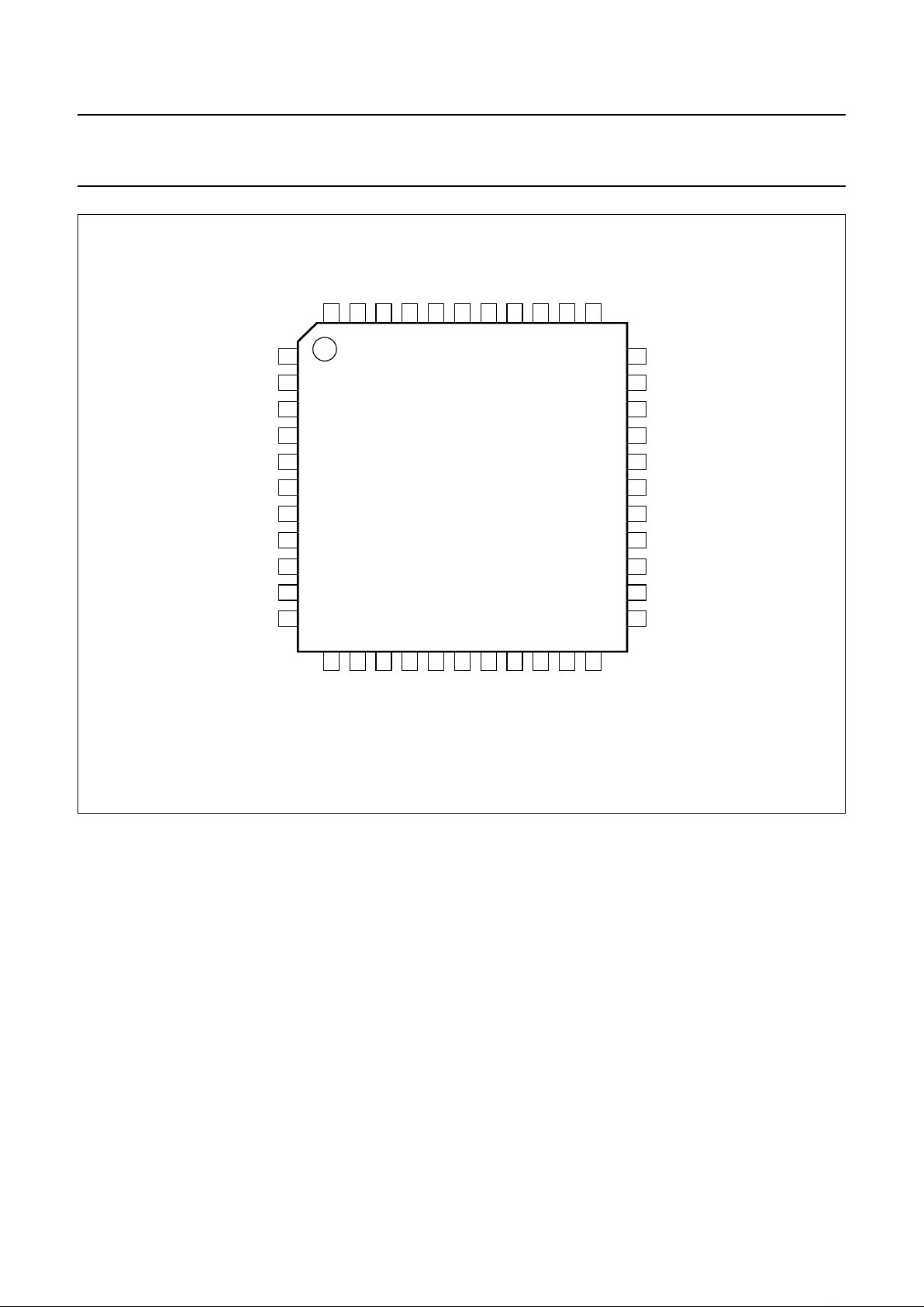
Fig.2 Pin configuration (QFP44).
handbook, full pagewidth
OM4068H
MBK814
1SEG30
SEG31
SEG32
M0
M1
SDIN
SCLK
SCE
SDOUT
BP1
BP2
BP3
SEG1
SEG2
SEG3
SEG4
SEG5
SEG6
SEG7
SEG8
SEG9
SEG10
SEG11
SEG12
SEG13
SEG14
SEG15
SEG16
SEG17
SEG18
SEG19
SEG20
SEG21
SEG22
SEG23
SEG24
SEG25
SEG26
SEG27
SEG28
SEG29
V
LCD
V
DD
V
SS
2
3
4
5
6
7
8
9
10
11
33
32
31
30
29
28
27
26
25
24
23
12
13
14
15
16
17
18
19
20
21
22
44
43
42
41
40
39
38
37
36
35
34
1998 Jun 18 7
Philips Semiconductors Product specification
LCD driver for low multiplex rates
OM4068
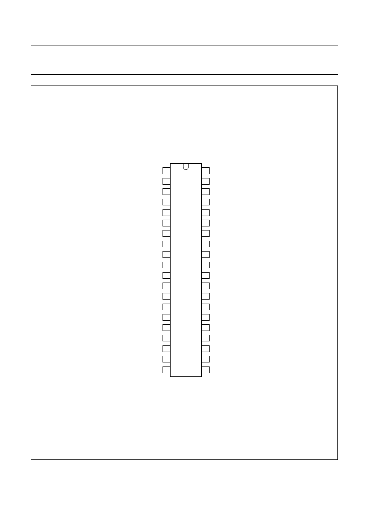
Fig.3 Pin configuration (DIP40).
handbook, halfpage
OM4068P
MBK815
1
2
3
4
5
6
7
8
9
10
11
12
13
14
15
16
17
18
19
20
40
39
38
37
36
35
34
33
32
31
30
29
28
27
26
25
24
23
22
21
SEG13 SEG12
SEG14 SEG11
SEG16 SEG10
SEG17 SEG9
SEG18 SEG8
SEG19 SEG7
SEG20 SEG5
SEG21 SEG4
SEG22 SEG3
SEG23 SEG2
SEG24 BP3
SEG26 BP2
SEG27 BP1
SEG28 SDOUT
SEG29 SCE
SEG30 SCLK
SEG31 SDIN
SEG32 M1
V
LCD
M0
V
DD
V
SS
1998 Jun 18 8
Philips Semiconductors Product specification
LCD driver for low multiplex rates
OM4068
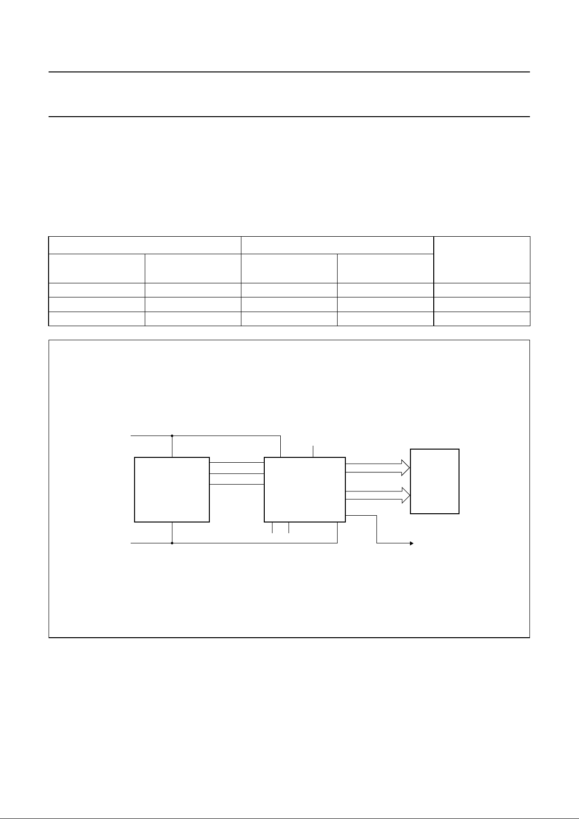
FUNCTIONAL DESCRIPTION
The OM4068 is a low-power LCD driver designed to
interface with any microprocessor/microcontroller and a
wide variety of LCDs. It can drive any static or multiplexed
LCD containing up to three backplanes and
up to 96 segments.
The display configurations possible with the OM4068
depend on the number of active backplane outputs
required; a selection of display configurations is given in
Table 1.
A typical system (MUX 1 : 3) is shown in Fig.4.
Table 1 Selection of display configurations
NUMBER OF 7-SEGMENTS NUMERIC
DOT MATRIX
BACKPLANES
DISPLAY
SEGMENTS
DIGITS
INDICATOR
SYMBOLS
3 96 12 12 96 dots (3 × 32)
2 64 8 8 64 dots (2 × 32)
1 32 4 4 32 dots (1 × 32)
Fig.4 Typical system configuration.
handbook, full pagewidth
HOST
MICROPROCESSOR/
MICROCONTROLLER
SCLK
SDOUT
SCE
SDIN
32 segment drivers
(1)
3 backplanes
LCD PANEL
(up to 96
elements)
OM4068
M1 M0
V
DD
V
DD
V
LCD
V
SS
V
SS
MBK818
(1) 28 segment drivers for DIP40 package.
The host microprocessor/microcontroller maintains the
3-line bus communication channel with OM4068.
The internal oscillator requires no external components.
The appropriate intermediate biasing voltage for the
multiplexed LCD waveforms are generated on-chip.
The only other connections required to complete the
system are to the power supplies (VSS, VDDand V
LCD
) and
suitable capacitors to decouple the V
LCD
and VDD pins to
VSS.
1998 Jun 18 9
Philips Semiconductors Product specification
LCD driver for low multiplex rates
OM4068
Power-on reset
The on-chip power-on reset block initializes the chip after
power-on or power failures. The OM4068 resets to a
starting condition as follows:
• All backplane and segment outputs are set to V
SS
(display off)
• All shift registers and latches are set in 3-state
• SDOUT (allowing serial cascading) is set to logic 0 (with
SCE LOW)
• Power-down mode.
Data transfers on the serial bus should be avoided for
0.5 ms following power-on to allow completion of the reset
action.
Power-down
After power-on the chip is in power-down mode as long as
the serial clock is not active. During power-down all static
currents are switched off (no internal oscillator, no timing
and no bias level generation) and all LCD-outputs are
3-stated. The power-on reset functions remain enabled.
The power-down mode is disabled at the first rising edge
of the serial clock SCLK.
LCD bias voltage generator
The intermediate bias voltages for the LCD display are
generated on-chip. This removes the need for an external
resistive bias chain and significantly reduces the system
power consumption. The full-scale LCD voltage V
OP
equals V
LCD
− VSS. The optimum value of VOP depends on
the LCD threshold voltage (Vth) and the number of bias
levels.
Fractional LCD biasing voltages are obtained from an
internal voltage divider of three series resistors (1⁄3bias)
connected between V
LCD
and VSS. The centre resistor can
be switched out of the circuit to provide a1⁄2bias voltage
level for the 1 : 2 multiplex configuration.
The bias levels depend on the multiplex rate and are
selected automatically when the display configuration is
selected using M1 and M0.
LCD voltage selector
The LCD voltage selector (control logic) coordinates the
multiplexing of the LCD in accordance with the selected
drive or display configuration. The operation of the voltage
selector is controlled by the input pins M0 and M1
(see Table 2).
Table 2 Drive mode selection
For multiplex rates of 1 : 2 three bias levels are used
including V
LCD
and VSS. Four bias level are used for the
1 : 3 multiplex rate. The various biasing configurations
together with the biasing characteristics as functions of
VOP=V
LCD
− VSS and the resulting discrimination ratios
(D), are given in Table 3.
A practical value for VOP is determinated by equating
V
off(rms)
with a defined LCD threshold voltage (Vth),
typically when the LCD exhibits approximately 10%
contrast. In static mode a suitable choice is VOP>3Vth.
M1 M0 DRIVE MODE
0 0 test mode (not user accessible)
0 1 static drive (1 : 1)
1 0 duplex drive (1 : 2)
1 1 triplex drive (1 : 3)
 Loading...