

Philips ne5090, sa5090 DATASHEETS
Philips Semiconductors Linear Products Product specification
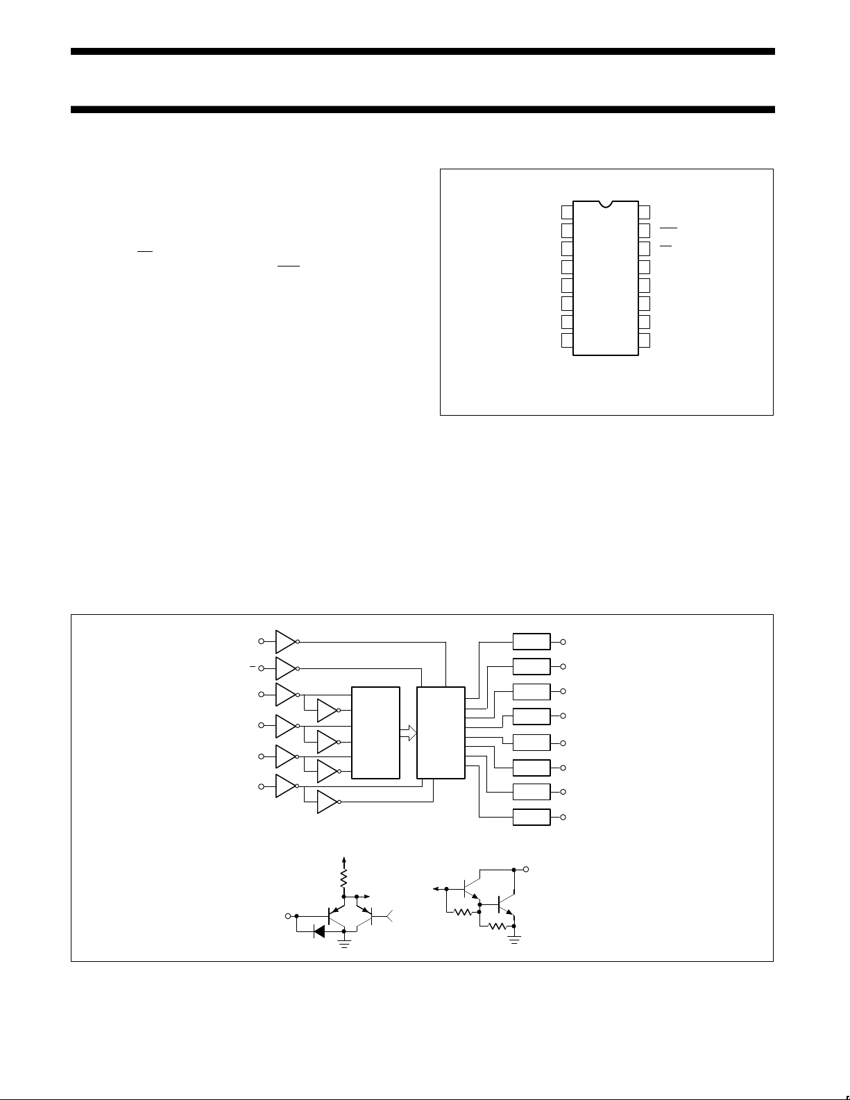
NE/SA5090Addressable relay driver
512
August 31, 1994 853-0892 13721
DESCRIPTION
The NE/SA5090 addressable relay driver is a high-current latched
driver, similar in function to the 9934 address decoder. The device
has 8 open-collector Darlington power outputs, each capable of
150mA load current. The outputs are turned on or off by respectively
loading a logic “1” or logic “0” into the device data input. The
required output is defined by a 3-bit address. The device must be
enabled by a CE
input line which also serves the function of further
address decoding. A common clear input, CLR
, turns all outputs off
when a logic “0” is applied. The device is packaged in a 16-pin
plastic or Cerdip package.
FEATURES
•8 high-current outputs
•Low-loading bus-compatible inputs
•Power-on clear ensures safe operation
•Will operate in addressable or demultiplex mode
•Allows random (addressed) data entry
•Easily expandable
•Pin-compatible with 9334 (Siliconix or Fairchild)
PIN CONFIGURATION
1
2
3
4
5
6
7
8
9
10
11
12
13
14
16
15
D1, N Packages
TOP VIEW
NOTE:
1. SOL - Released in Large SO package only.
A
0
A
1
A
2
Q
0
Q
1
Q
2
Q
3
GND
V
CC
CLR
CE
D
Q
7
Q
6
Q
5
Q
4
APPLICATIONS
•Relay driver
•Indicator lamp driver
•Triac trigger
•LED display digit driver
•Stepper motor driver
BLOCK DIAGRAM
LATCH
LATCH
LATCH
LATCH
LATCH
LATCH
LATCH
LATCH
CLR
CE
A
0
A
1
A
2
D
1–OF–8
DECODER
CONTROL
GATE
V
CC
OUTPUT STAGEINPUT STAGE
Q
0
Q
1
Q
2
Q
3
Q
4
Q
5
Q
6
Q
7
Philips Semiconductors Linear Products Product specification
NE/SA5090Addressable relay driver
August 31, 1994
513
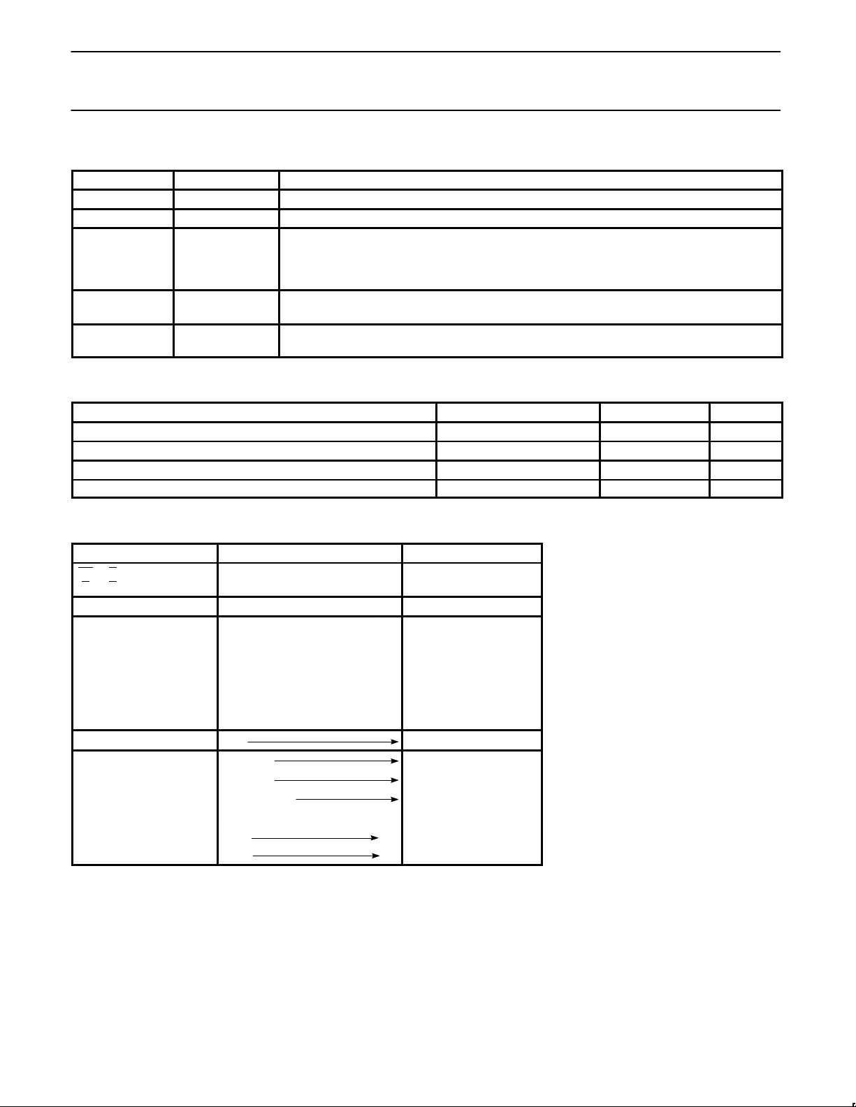
PIN DESIGNATION
PIN NO. SYMBOL NAME AND FUNCTION
1-3 A0-A
2
A 3-bit binary address on these pins defines which of the 8 output latches is to receive the data.
4-7, 9-12 Q0-Q
7
The 8 device outputs.
13 D The data input. When the chip is enabled, this data bit is transferred to the defined output such that:
“1” turns output switch “ON”
“0” turns output switch “OFF”
14 CE The chip enable. When this input is low, the output latches will accept data. When CE goes high, all
outputs will retain their existing state, regardless of address of data input condition.
15 CLR The clear input. When CLR goes low all output switches are turned “OFF”. The high data input will
override the clear function on the addressed latch.
ORDERING INFORMATION
DESCRIPTION TEMPERATURE RANGE ORDER CODE DWG #
16-Pin Plastic Small Outline Large (SOL) Package 0 to +70°C NE5090D 0171B
16-Pin Plastic Dual In-Line Package (DIP) 0 to +70°C NE5090N 0406C
16-Pin Plastic Dual In-Line Package (DIP) -40 to +85°C SA5090N 0406C
16-Pin Plastic Small Outline Large (SOL) Package –40 to +85°C SA5090D 0171B
TRUTH TABLE
INPUTS OUTPUTS MODE
CLRCED A0A1A2Q0Q1Q2Q3Q4Q5Q6Q
7
L H X X X X H H H H H H H H Clear
L L L L L L H H H H H H H H
L L H L L L L H H H H H H H
L L L H L L H H H H H H H H Demultiplex
L L H H L L H L H H H H H H
L L L H H H H H H H H H H H
L L H H H H H H H H H H H L
H H X X X X Q
N-1
Memory
H L L L L L H Q
N-1
H L H L L L L Q
N-1
H L L H L L Q
N-1
H Q
N-1
Addressable Latch
H L H H L L Q
N-1
L Q
N-1
H L L H H H Q
N-1
H
H L H H H H Q
N-1
L
NOTES:
X=Don’t care condition
Q
N-1
=Previous output state
L=Low voltage level/“ON” output state
H=High voltage level/“OFF” output state
 Loading...