

Philips ne5020 DATASHEETS
Philips Semiconductors Linear Products Product specification
NE502010-Bit µP-compatible D/A converter
757
August 31, 1994 853-0392 13721
DESCRIPTION
The NE5020 is a microprocessor-compatible monolithic 10-bit
digital-to-analog converter subsystem. This device offers 10-bit
resolution and ±0.1% accuracy and monotonicity guaranteed over
full operating temperature range.
Low loading latches, adjustable logic thresholds, and addressing
capability allow the NE5020 to directly interface with most
microprocessor- and logic-controlled systems.
The NE5020 contains internal voltage reference, DAC switches and
resistor ladder. Also, the input buffer and output summing amplifier
are included. In addition, the matched application resistors for
scaling either unipolar or bipolar output values are included on a
single monolithic chip.
The result is a near minimum component count 10-bit resolution
DAC system.
FEATURES
•10-bit resolution
•Guaranteed monotonicity over operating range
•±0.1% relative accuracy
•Unipolar (0V to +10V) and bipolar (± 5V) output range
•Logic bus compatible
•5µs settling time
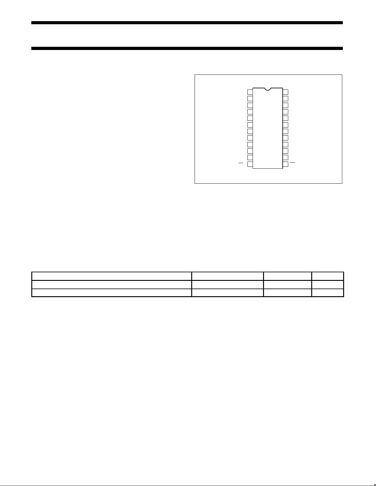
PIN CONFIGURATION
1
2
3
4
5
6
7
8
9
10
11
12
13
14
24
23
22
21
20
19
18
17
16
15
F, N Packages
DIGITAL GND
DB0(LSB)
DB1
DB2
DB3
DB4
DB5
DB6
DB7(MSB)
NC
ANALOG GND
AMP COMP
SUM MODE
BIPOLAR OFFSET R
LE
1
V
CC+
V
OUT
V
CC–
+V
REF
IN
V
REF
OUT
–V
REF
IN
V
REF
ADJ
LE
2
APPLICATIONS
•Precision 10-bit D/A converters
•10-bit analog-to-digital converters
•Programmable power supplies
•Test equipment
•Measurement instruments
ORDERING INFORMATION
DESCRIPTION TEMPERATURE RANGE ORDER CODE DWG #
24-Pin Ceramic Dual In-Line Package (CERDIP) 0 to 70°C NE5020F 0588B
24-Pin Plastic Dual In-Line Package (DIP) 0 to 70°C NE5020N 0412A
Philips Semiconductors Linear Products Product specification
NE502010-Bit µP-compatible D/A converter
August 31, 1994
758
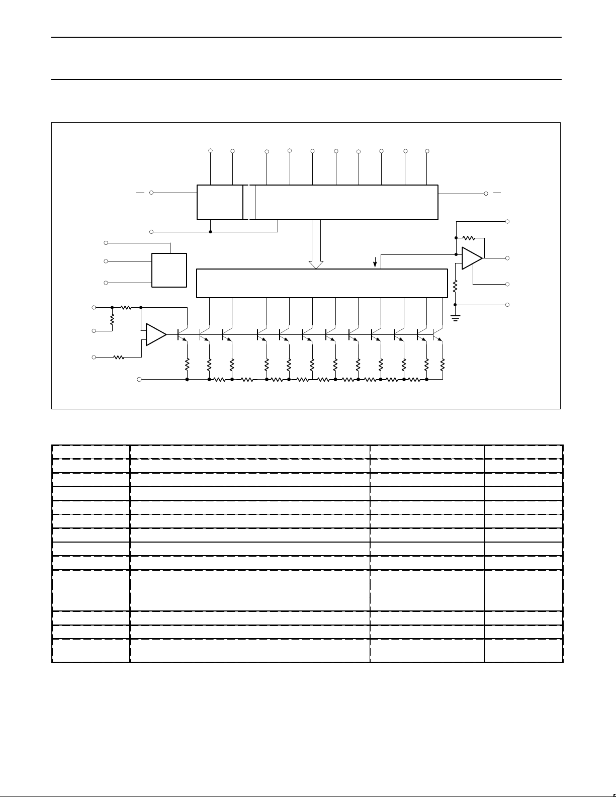
BLOCK DIAGRAM
(15)
(14)
(22)
(20)
(23)
(24)
(17)
(18)
BIPOLAR
OFFSET
+V
REF
IN
ANALOG
GND
AMP
COMP
SUM
NODE
DAC OUTPUT CURRENT
DAC SWITCHES
(19)
(13)
MSB
LSB
DIGITAL GND(1)
–V
CC
INT
V
REF
(11)
DB9
(10)
DB8
(9)
DB7
(8)
DB6
(7)
DB5
(6)
DB4
(5)
DB3
(4)
DB2
LE
2
V
OUT
+
–
V
REF
OUT
V
REF
ADJ
+
–
QRQ9Q
8
Q7Q6Q5Q4Q3Q2Q1Q
0
Q
T
(3)
DB1
(2)
DB0
LATCHES AND
SWITCH DRIVERS
(12)
LE
1
(21)
+V
CC
R
BIP
R
REF
R
(16)
–V
REF
IN
R
R
fb
ABSOLUTE MAXIMUM RATINGS
SYMBOL PARAMETER RATING UNIT
V
CC
+
Positive supply voltage 18 V
V
CC
-
Negative supply voltage -18 V
V
IN
Logic input voltage 0 to 18 V
V
REF IN
Voltage at +V
REF
input 12 V
V
REF ADJ
Voltage at V
REF
adjust 0 to V
REF
V
V
SUM
Voltage at sum node 12 V
I
REFSC
Short-circuit current to ground at V
REF OUT
Continuous
I
OUTSC
Short-circuit current to ground or either supply at V
OUT
Continuous
P
D
Maximum power dissipation TA=25°C, (still-air)
1
F package 2150 mW
N package 2150 mW
T
A
Operating temperature range NE5020 0 to +70 °C
T
STG
Storage temperature range -65 to +150 °C
T
SOLD
Lead soldering temperature
(10 sec. max)
300 °C
NOTES:
1. Derate above 25°C at the following rates:
F package at 17.2mW/°C
N package at 17.2mW/°C
Philips Semiconductors Linear Products Product specification
NE502010-Bit µP-compatible D/A converter
August 31, 1994
759
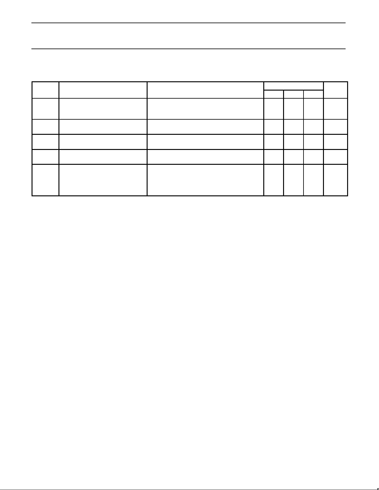
DC ELECTRICAL CHARACTERISTICS
VCC+=+15V, VCC-=-15V, 0 ≤ TA≤70°C, unless otherwise specified.1 Typical values are specified at 25°C.
LIMITS
SYMBOL
PARAMETER
TEST CONDITIONS
Min Typ Max
UNIT
Resolution
Monotonicity
Relative accuracy
10
10
±0.1
Bits
Bits
%FS
V
CC+
V
CC-
Positive supply voltage
Negative supply voltage
11.4
-11.415-15
16.5
-16.5
V
V
V
IN(1)
V
IN(0)
Logic “1” input voltage
Logic “0” input voltage
Pin 1=0V
Pin 1=0V
2.0
0.8
V
V
I
IN(1)
I
IN(0)
Logic “1” input current
Logic “0” input current
Pin 1=0V, 2<VIN<18V
Pin 1=0V, -5V<V
IN
<0.8V
0.1
-2.010-10
µA
µA
V
FS
Full-scale output
Unipolar mode, V
REF
=5.000V, all bits high,
T
A
=25°C
9.5 10.5 V
+V
FS
Full-scale output Bipolar mode, V
REF
=5.000V, all bits high, TA=25°C 4.75 5.25 V
-V
FS
Negative full-scale Bipolar mode, V
REF
=5.000V, all bits low, TA=25°C -5.25 -4.75 V
NOTES:
1. Refer to Figure 1.
 Loading...