

Philips N74F583D, N74F583N Datasheet

INTEGRATED CIRCUITS
74F583
4-bit BCD adder
Product specification
IC15 Data Handbook
1989 Apr 06
Philips Semiconductors Product specification
74F5834-bit BCD adder
FEA TURES
•Adds two decimal numbers
•Full internal look-ahead
•Fast ripple carry for economical expansion
•Sum output delay 19.5 ns max.
•Ripple carry delay 8.5 ns max.
•Input to ripple delay 13.0 ns max.
•Supply current 60 mA max.
DESCRIPTION
The 74F583 4-bit coded (BCD) full adder performs the addition of
two decimal numbers (A0–A3, B0–B3). The look-ahead generates
BCD carry terms internally, allowing the 74F583 to then do BCD
addition correctly . For BCD numbers 0 through 9 at A and B inputs,
the BCD sum forms at the output.
In addition of two BCD numbers totalling a number greater than 9, a
valid BCD number and carry will result. For input values larger than
9, the number is converted from binary to BCD. Binary to BCD
conversion occurs by grounding one set of inputs, An or Bn, and
applying a 4-bit binary number to the other set of inputs. If the input
is between 0 and 9, a BCD number occurs at the output. If the
binary input falls between 10 and 15, a carry term is generated. Both
the carry term and the sum are the BCD equivalent of the binary
input. Converting binary numbers greater than 16 may be achieved
by cascading 74F583s.
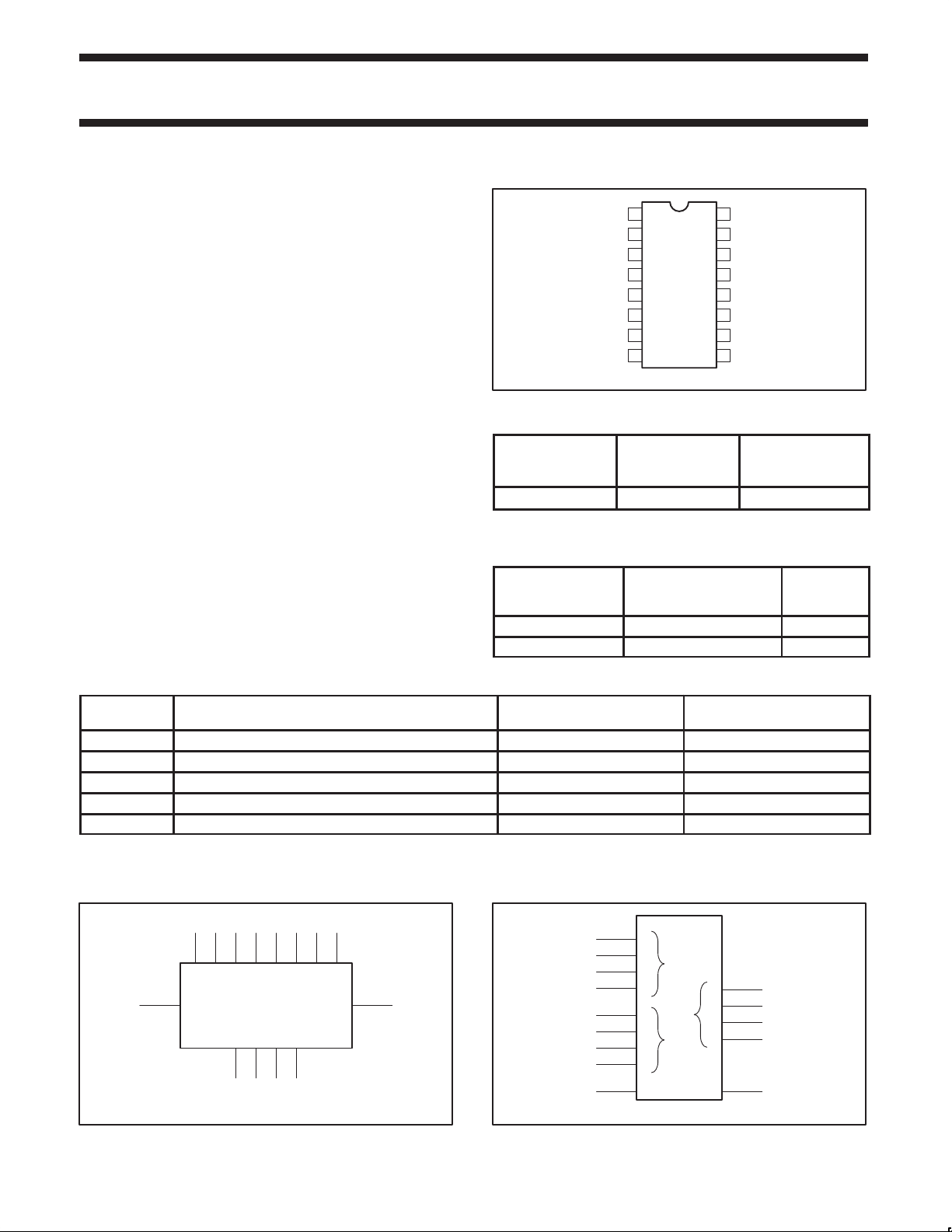
PIN CONFIGURATION
1
2
B2
3
B3
4
A3
5
C
n
6
C
n+4
7
S2
89
GND
TYPICAL
TYPE
PROPAGATION
DELAY
74F583 9.0 ns 45 mA
16B1
V
CC
15
A2
14
A1
13
A0
12
B0
11
S0
10
S1
S3
SF01436
SUPPLY CURRENT
TYPICAL
(TOTAL)
ORDERING INFORMA TION
COMMERCIAL RANGE
PACKAGE
VCC = 5 V ±10%
= 0°C to +70°C
T
amb
16-pin plastic DIP N74F583N SOT38-4
16-pin plastic SO N74F583D SOT109-1
DRAWING
NUMBER
INPUT AND OUTPUT LOADING AND FAN-OUT TABLE
PINS DESCRIPTION 74F (U.L.)
HIGH / LOW
A0–A3 A operand inputs 1.0 / 2.0 20 µA / 1.2 mA
B0–B3 B operand inputs 1.0 / 2.0 20 µA / 1.2 mA
C
n
C
n+4
Carry input 1.0 / 1.0 20 µA / 0.6 mA
Carry output 50 / 33 1.0 mA / 20 mA
S0–S3 Sum outputs 50 / 33 1.0 mA / 20 mA
NOTE:
One (1.0) FAST Unit Load is defined as 20 µA in the High state and 0.6 mA in the Low state.
LOGIC SYMBOL
= Pin 16
V
CC
GND = Pin 8
A0 B0 A1 B1 A2 B2 A3 B3
C
n
S0 S1 S2 S3
11 10 7 9
C
n+4
342151141213
65
SF01437
LOGIC SYMBOL (IEEE/IEC)
13
14
15
4
12
1
2
3
5
Σ (BCD)
0
P
3
0
Q
3
Σ
LOAD VALUE
HIGH / LOW
0
3
COCI
SF01438
11
10
7
9
6
1989 Apr 06 853–1245 96263
2
Philips Semiconductors Product specification
74F5834-bit BCD adder
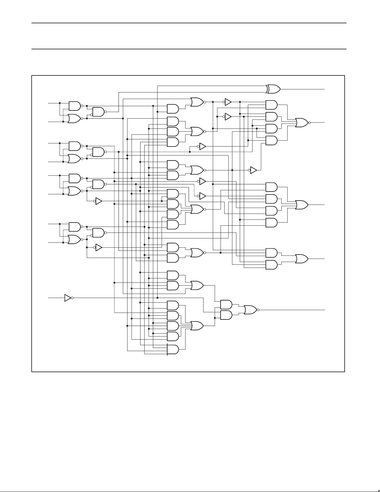
LOGIC DIAGRAM
11
S0
12
B0
13
A0
1
B1
14
A1
2
B2
15
A2
3
B3
4
A3
5
C
n
10
S1
7
S2
9
S3
6
C
n+4
V
= PIN 16
CC
GND = PIN 8
1989 Apr 06
SF01435
3
 Loading...