

Philips N74F524N, N74F524D Datasheet

INTEGRATED CIRCUITS
74F524
8-bit register comparator (open-collector
+ 3-State)
Product specification
IC15 Data Handbook
1990 Aug 07
Philips Semiconductors Product specification
74F5248-bit register comparator (open collector + 3-State)
FEA TURES
•8-Bit bidirectional register with bus-oriented input-output
•Independent serial input-output to register
•Register bus comparator with ‘equal to’, ‘greater than’ and
‘less than’ outputs
•Cascadable in groups of 8-bits
•Open collector comparator outputs for AND-wired expansion
•Two’ s complement or magnitude compare
DESCRIPTION
The 74F524 is an 8-bit bidirectional register with parallel input and
output, plus serial input and output progressing from MSB to LSB.
All data inputs, serial and parallel, are loaded by the rising edge of
the clock. The device functions are controlled by two control lines
(S0, S1) to execute shift, load, hold and read out. An 8-bit
comparator examines the data stored in the registers and on the
data bus. Three true-High, open collector outputs representing
‘register equal to bus’, ‘register greater than bus’ and ‘register less
than bus’ are provided. These outputs can be disabled to the OFF
state by the use of Status Enable (SE
been provided to allow Two’s Complement as well as magnitude
compare. Linking inputs are provided for expansion to longer words.
). A mode control has also
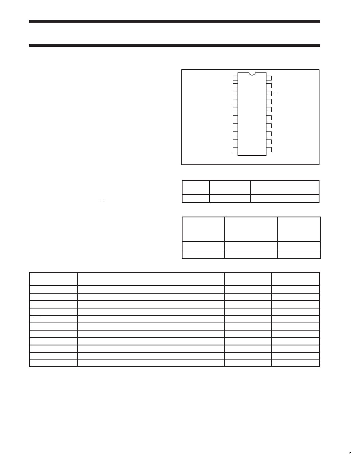
PIN CONFIGURATION
S0
1
I/O0
2
3
I/O1
I/O2
4
I/O3
5
I/O4
6
I/O5
7
I/O6
8
I/O7
9
GND CP
TYPE TYPICAL f
TYPICAL SUPPL Y CURRENT
MAX
74F524 65MHz 110mA
20
19
18
17
16
15
14
13
12
1110
SF00970
V
CC
S1
SE
C/SI
C/SO
EQ
GT
LT
M
(TOTAL)
ORDERING INFORMATION
COMMERCIAL
DESCRIPTION
20-pin plastic DIP N74F524N SOT146-1
20-pin plastic SOL N74F524D SOT163-1
RANGE
V
= 5V ±10%,
CC
T
= 0°C to +70°C
amb
PKG DWG #
INPUT AND OUTPUT LOADING AND FAN-OUT TABLE
PINS DESCRIPTION
74F(U.L.)
HIGH/LOW
I/On Parallel data inputs 3.5/1.0 70µA/0.6mA
S0, S1 Mode select inputs 1.0/1.0 20µA/0.6mA
C/SI Status priority or serial data input 1.0/1.0 20µA/0.6mA
CP Clock pulse input (active rising edge) 1.0/1.0 20µA/0.6mA
SE Status enable input (active Low) 1.0/1.0 20µA/0.6mA
M Compare mode select input 1.0/1.0 20µA/0.6mA
I/On 3-state parallel data outputs 150/40 3.0mA/24mA
C/SO Status priority or serial data output 50/33 1.0mA/20mA
LT Register less than bus output OC/33 OC/20mA
EQ Register equal to bus output OC/33 OC/20mA
GT Register greater than bus output OC/33 OC/20mA
NOTE:
One (1.0) FAST Unit Load (U.L.) is defined as 20µA in the High state and 0.6mA in the Low state.
OC=Open Collector
LOAD VALUE
HIGH/LOW
1990 Aug 07 853–0373 00135
2
Philips Semiconductors Product specification
74F5248-bit register comparator (open collector + 3-State)
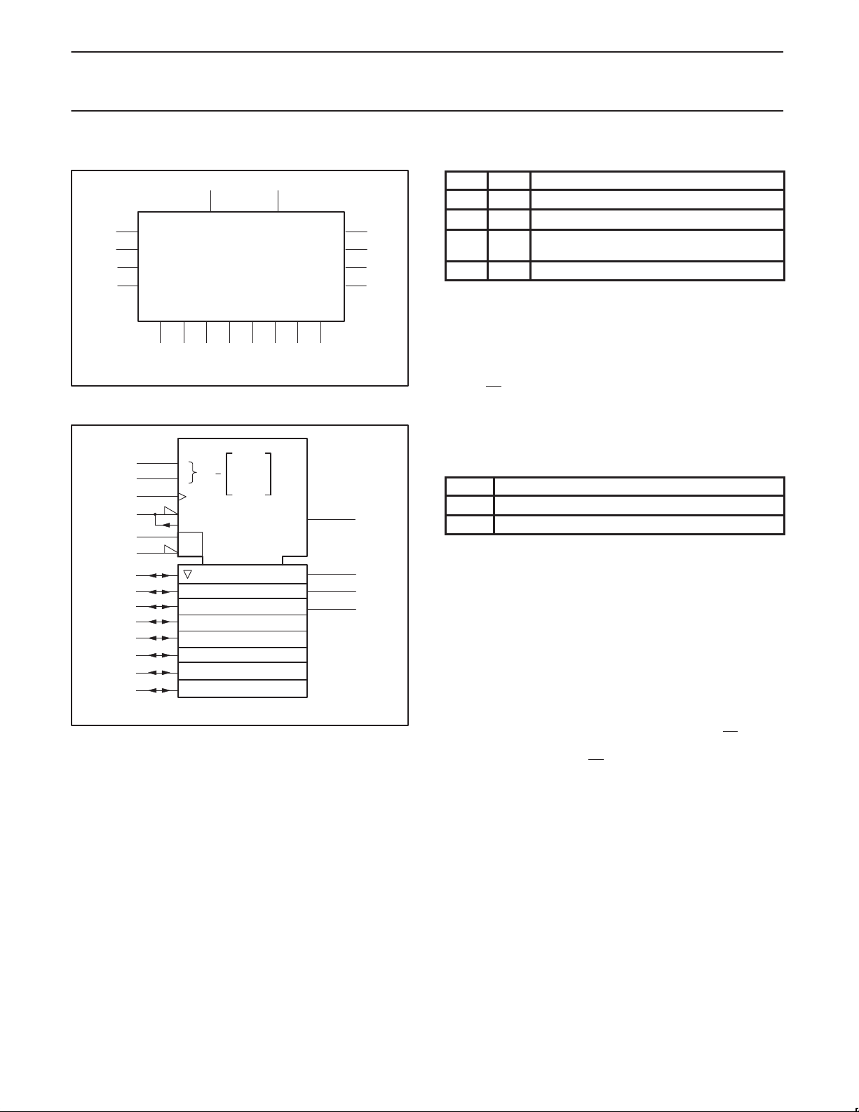
LOGIC SYMBOL for 74F456
12 18
MSE
C/SO 16
LT
GT
EQ
13
14
15
SF00971
1
19
11
VCC= Pin 20
GND = Pin 10
C/SI17
S0
S1
CP
I/O0 I/O1 I/O2 I/O3 I/O4 I/O5 I/O6 I/O7
23456789
LOGIC SYMBOL (IEEE/IEC) for 74F456
COMP
1
19
12
17
18
0
1
11
2
3
4
5
6
7
8
9
C4/2/4
M5 MAGNITUDE
M6 TWO’s COMPLEMENT
&
M
3, 4D
G7
0
3
0=HOLD
1=READ
2=SHIFT
3=LOAD
1,5,6,7>I/O
1,5,6,7<I/O
1,5,6,7=I/O
2D
16
13
14
15
SF00972
FUNCTIONAL DESCRIPTION
The 74F524 contains eight D-type flip-flops connected as a shift
register with provision for either parallel or serial loading. Parallel
data may be read from or loaded into the registers via the data bus
I/O0–I/O7. Serial data is loaded into the register from the C/SI input
and may be shifted through the register and out through the C/SO
output. Both parallel and serial data entry occurs on the rising edge
of the clock (CP). The operation of the shift register is controlled by
two signals, S0 and S1, according to the Select Function Table. The
3-State parallel output buffers are enabled only in the READ mode.
SELECT FUNCTION TABLE
S0 S1 OPERATION
L L HOLD–Retains data in shift register
L H READ–Read contents in register onto data bus
H L SHIFT–Allows serial shifting on next rising clock
edge
H H LOAD–Load data on bus into register
H = High voltage level
L = Low voltage level
One port of an 8-bit comparator is attached to the data bus while the
other port is tied to the outputs of the internal register. Three
active-OFF Open Collector outputs indicate whether the contents
held in the shift register are ‘greater than’ (GT). ‘less than’ (LT), or
‘equal to’ (EQ) the data on the input bus. A High signal on the Status
Enable (SE
) input disables these outputs to the OFF state. A mode
control (M) input allows selection between a straightforward
magnitude compare or a comparison between Two’s complement
numbers.
NUMBER REPRESENTA TION SELECT TABLE
M OPERATION
L Magnitude compare
H Two’s Complement compare
H = High voltage level
L = Low voltage level
For ‘greater than’ or ‘less than’ detection, the C/SI input must be
held High, as indicated in the Function Table. The internal logic is
arranged such that a Low signal on the C/SI input places the
‘greater than’ and ‘less than’ outputs in their off state. (Note that this
off state serves also as the active state when C/SI is High. It is
intended for use in expansion to word lengths greater than 8 bits
using multiple 74S524s as explained in the next 3 paragraphs.) The
C/SO output will be forced High if the ‘equal to’ status condition
exists; otherwise, C/SO will be held Low.
Word length expansion (in groups of 8 bits) can be achieved by
connecting the C/SO output of the more significant byte to the C/SI
input of the next less significant byte and also to its own SE
(see Application Figure 1). The CS/I input of the most significant
device is held High while the SE
input of the least significant device
is held Low. The corresponding status outputs are AND-wired
together. In the case of two’s complement number compare, only the
Mode input to the most significant device should be High. the Mode
inputs to all other cascaded devices are held Low.
Suppose that an inequality condition is detected in the most
significant device. Assuming that the byte stored in the register is
greater than the byte on the data bus, then the EQ and LT outputs
will be pulled Low, whereas the GT output will float High. Also, the
input
1990 Aug 07
3

Philips Semiconductors Product specification
OPERATING MODE
Hold
Read
Load
(GT=CT=off)
(GT=CT=on)
74F5248-bit register comparator (open collector + 3-State)
CS/O output of the most significant device will be forced Low,
disabling the subsequent devices but enabling its own status
outputs. The corrected status condition is thus indicated. The same
applies if the register byte is less than the data byte, only in this
case the EQ and GT outputs go Low, whereas the LT output floats
High.
If an equality condition is detected in the most significant device, its
C/SO output is forced High. This enables the next less significant
APPLICATION
GREATER THAN
EQUAL TO
LESS THAN
H = TWO’s COMPLEMENT
L = MAGNITUDE
H
RD
WR
MGTEQLT
C/SI
S0 S1 I/O
C/SO
SE
C/SI
device and disables its own status outputs. In this way, the status
output proximity is handed down to the next less significant device
which now effectively becomes the most significant byte. The worst
case propagation delay for a compare operation involving ‘n’
cascaded 74F524s will be when an equality condition is detected in
all but the least significant byte. In this case, the status priority has
to ripple all the way down the chain before the correct status output
is established. Typically, this will take 35+6(n–2) ns.
LL
MGTEQLT
SE
C/SO
S0 S1 I/O
MGTEQLT
C/SI
S0 S1 I/O
SE
C/SO
V
CC
L
MSB
8
8 8LSB
Figure 1. Cascading 74F524s for Comparing Longer Words
FUNCTION TABLE
INPUTS OUTPUTS
SE C/SI S0 S1 Data comparison EQ GT LT C/SO
H H L L X H H H (1)
H L L L X H H H L
H X H L X H H H Q0 Shift
H H L H X H H H (1)
H L L H X H H H L
H H H H X H H H (1)
H L H H X H H H L
L L H or L
L L H or L
L L H or L
L H H or L
L H H or L
L H H or L
2
2
2
2
2
2
(1) = High if I/On=Dn, otherwise Low
2 = Must meet setup and hold time requirements
H = High voltage level
L = Low voltage level
X = Don’t care
H or L
H or L
H or L
H or L
H or L
H or L
2
2
2
2
2
2
OA–OH > I/O0–I/O7 L H H L
OA–OH = I/O0–I/O7 H H H L
OA–OH < I/O0–I/O7 L H H L
OA–OH > I/O0–I/O7 L H L L
OA–OH = I/O0–I/O7 H L L H
OA–OH < I/O0–I/O7 L L H L
Compare
=
=
Compare
=
=
SF01012
1990 Aug 07
4

Philips Semiconductors Product specification
74F5248-bit register comparator (open collector + 3-State)
LOGIC DIAGRAM
1
S0
19
C/SI
S1
SE
18
17
16
C/SO
15
EQ
I/O0
I/O1
I/O2
I/O3
I/O4
2
3
4
5
6
CP
DQQ
CP
DQQ
CP
DQQ
CP
DQQ
CP
DQQ
14
GT
7
I/O5
8
I/O6
9
I/O7
11
CP
12
M
VCC= Pin 20
GND = Pin 10
1990 Aug 07
CP
DQQ
CP
DQQ
CP
DQQ
13
LT
SF00973
5
 Loading...