

Philips N74F51D, N74F51N Datasheet
INTEGRATED CIRCUITS
74F51
Dual 2-wide 2-input, 2-wise 3-input
AND-OR-invert gate
Product specification
IC15 Data Handbook
1989 Mar 03
Philips Semiconductors Product specification
74F51Dual 2-wide 2-input, 2-wide 3-input AND-OR-invert gate
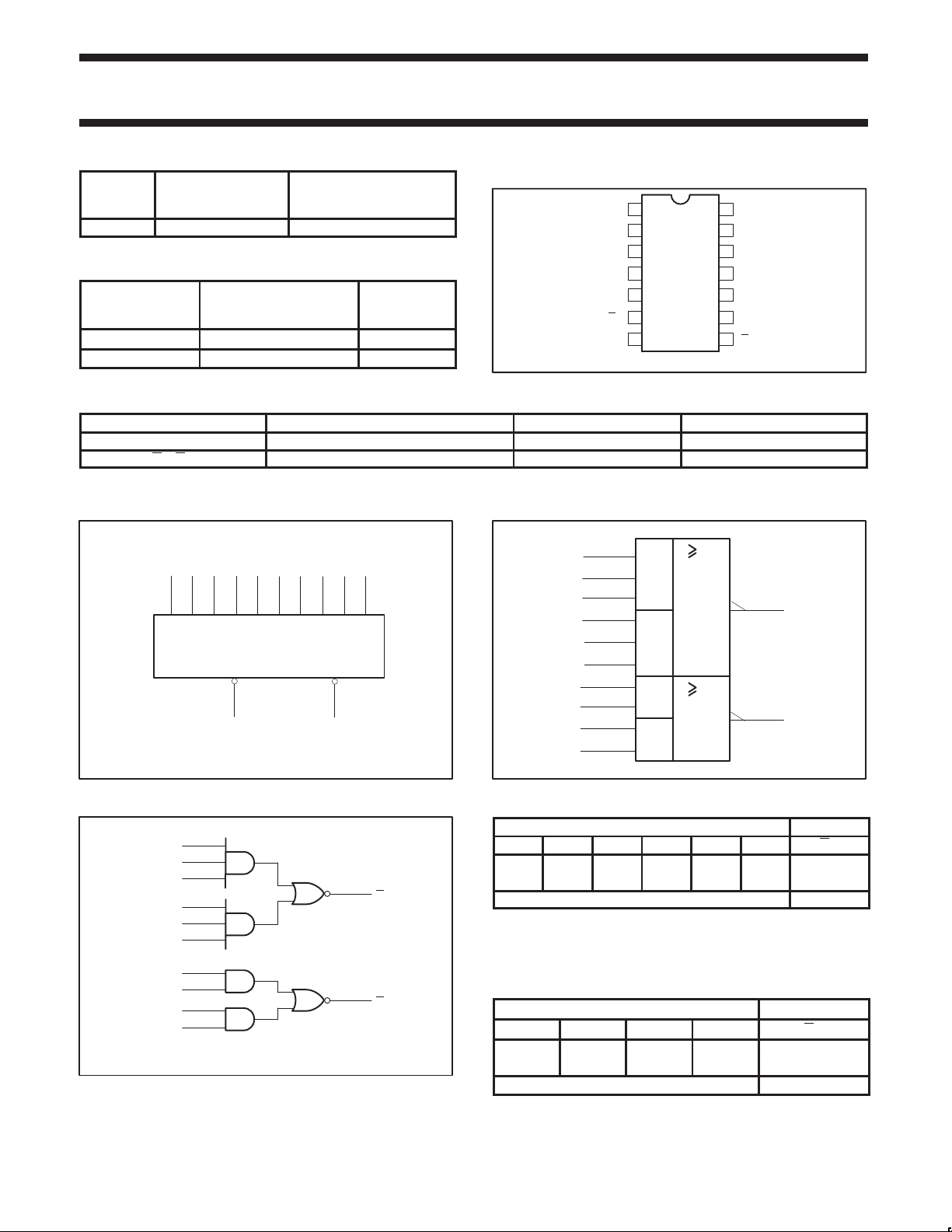
TYPE
TYPICAL
PROPAGATION
DELA Y
TYPICAL
SUPPLY CURRENT
(TOTAL)
74F51 3.0ns 3.5mA
ORDERING INFORMATION
COMMERCIAL RANGE
V
DESCRIPTION
14-pin plastic DIP N74F51N SOT27-1
14-pin plastic SO N74F51D SOT108-1
= 5V ±10%,
CC
= 0°C to +70°C
T
amb
PKG DWG #
PIN CONFIGURATION
D0a
1
D1a
2
D1b
3
D1c
4
D1d
5
1
Q
6
GND
14
V
D0c
13
D0b
12
D0f
11
D0e
10
D0d
9
Q0
87
SF00085
CC
INPUT AND OUTPUT LOADING AND FAN-OUT TABLE
PINS DESCRIPTION 74F (U.L.) HIGH/LOW LOAD VALUE HIGH/LOW
Dna, Dnb, Dnc, Dnd, Dne, Dnf Data inputs 1.0/1.0 20µA/0.6mA
Q0, Q1 Data outputs 50/33 1.0mA/20mA
NOTE: One (1.0) FAST unit load is defined as: 20µA in the High state and 0.6mA in the Low state.
LOGIC SYMBOL
1
D0a
VCC = Pin 14
GND = Pin 7
12 13 9 10 11 2 3 4
D1aD0fD0b D0c D0d D1b D1cD0e
Q0 Q1
86
5
D1d
SF00086
IEC/IEEE SYMBOL
9
10
11
13
12
1
2
3
4
5
&
1
8
&
&
1
6
&
SF00087
LOGIC DIAGRAM
FUNCTION TABLE FOR 3-INPUT GATES
INPUTS OUTPUT
VCC = Pin 14
GND = Pin 7
D0a
D0b
D0c
D0d
D0e
D0f
D1a
D1b
D1c
D1d
1
12
13
9
10
11
2
3
4
5
8
6
SF00088
Q0
Q1
D0a D0b D0c D0d D0e D0f Q0
H H H X X X L
X X X H H H L
All other combinations H
NOTES:
H = High voltage level
L = Low voltage level
X = Don’t care
FUNCTION TABLE FOR 2-INPUT GATES
INPUTS OUTPUT
D1a D1b D1c D1d Q1
H H X X L
X X H H L
All other combinations H
NOTES:
H = High voltage level
L = Low voltage level
X = Don’t care
March 3, 1989 853–0054 95962
2
Philips Semiconductors Product specification
SYMBOL
PARAMETER
UNIT
SYMBOL
PARAMETER
TEST CONDITIONS
1
UNIT
VOHHigh-level output voltage
VOLLow-level output voltage
ICCSupply current (total)
V
MAX
74F51Dual 2-wide 2-input, 2-wide 3-input AND-OR-invert gate
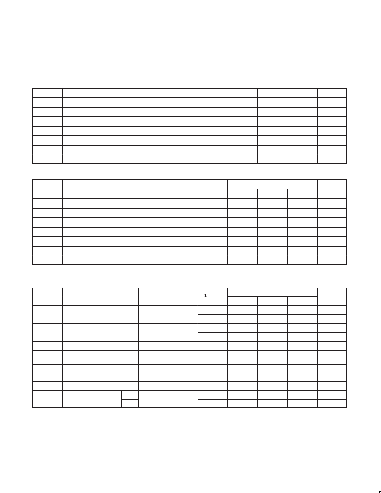
ABSOLUTE MAXIMUM RATINGS
(Operation beyond the limits set forth in this table may impair the useful life of the device.
Unless otherwise noted these limits are over the operating free-air temperature range.)
SYMBOL
V
V
I
IN
V
I
OUT
T
T
CC
IN
OUT
amb
stg
Supply voltage –0.5 to +7.0 V
Input voltage –0.5 to +7.0 V
Input current –30 to +5 mA
Voltage applied to output in High output state –0.5 to V
Current applied to output in Low output state 40 mA
Operating free-air temperature range 0 to +70 °C
Storage temperature range –65 to +150 °C
RECOMMENDED OPERATING CONDITIONS
V
V
V
I
I
I
T
CC
IH
IL
IK
OH
OL
amb
Supply voltage 4.5 5.0 5.5 V
High-level input voltage 2.0 V
Low-level input voltage 0.8 V
Input clamp current –18 mA
High-level output current –1 mA
Low-level output current 20 mA
Operating free-air temperature range 0 +70 °C
PARAMETER RATING UNIT
CC
V
LIMITS
MIN NOM MAX
DC ELECTRICAL CHARACTERISTICS
(Over recommended operating free-air temperature range unless otherwise noted.)
LIMITS
MIN TYP
p
p
V
IK
I
I
I
IH
I
IL
I
OS
Input clamp voltage VCC = MIN, II = I
Input current at maximum input
voltage
High-level input current VCC = MAX, VI = 2.7V 20 µA
Low-level input current VCC = MAX, VI = 0.5V –0.6 mA
Short-circuit output current
pp
VCC = MIN, VIL = MAX ±10%V
VIH = MIN, IOH = MAX ±5%V
VCC = MIN, VIL = MAX ±10%V
VIH = MIN, IOL = MAX ±5%V
IK
VCC = MAX, VI = 7.0V 100 µA
3
VCC = MAX –60 –150 mA
I
CCH
I
CCL
CC
=
CC
CC
CC
CC
VIN = GND 1.8 3.0 mA
VIN = 4.5V 5.5 7.5 mA
2.5 V
2.7 3.4 V
NOTES:
1. For conditions shown as MIN or MAX, use the appropriate value specified under recommended operating conditions for the applicable type.
2. All typical values are at V
3. Not more than one output should be shorted at a time. For testing I
= 5V, T
CC
techniques are preferable in order to minimize internal heating and more accurately reflect operational values. Otherwise, prolonged shorting
amb
= 25°C.
, the use of high-speed test apparatus and/or sample-and-hold
OS
of a High output may raise the chip temperature well above normal and thereby cause invalid readings in other parameter tests. In any
sequence of parameter tests, I
tests should be performed last.
OS
2
MAX
0.30 0.50 V
0.30 0.50 V
–0.73 –1.2 V
March 3, 1989
3
 Loading...