

Philips N74F399N Datasheet
INTEGRATED CIRCUITS
74F398*, 74F399
Registers
* Discontinued part. Please see the Discontinued Product List.
Product specification
Supersedes data of 1990 Apr 08
IC15 Data Handbook
1999 Jan 08
Philips Semiconductors Product specification
74F398*,74F399Registers
74F398 Quad 2-Port Register with True and Complementary Outputs
74F399 Quad 2-Port Register
FEATURES
•Select inputs from two data sources
•Fully positive edge-triggered
•Both True and Complementary outputs–74F398
DESCRIPTION
The 74F398 and 74F399 are the logical equivalent of a quad 2-input
multiplexer feeding into four edge-triggered flip-flops. A common
Select input determines which of two 4-bit words is accepted. The
selected data enters the flip-flops on the rising edge of the clock.
The 74F399 is the 16-pin version of the 74F398, with only the true
(Qn) outputs of the flip-flops available.
The 74F398 and 74F399 are high speed quad 2-port registers. They
select 4 bits of data from either of two sources (Ports) under control
of a common select input (S). The selected data is transferred to a
4-bit output register synchronous with the Low-to-High transition of
the Clock input (CP). The 4-bit D-type output register is fully
edge-triggered. The Data inputs (I0n, I1n) and Select input (S) must
be stable only a setup time prior to and hold time after the
Low-to-High transition of the Clock input for predictable operation.
The 74F398 has both Q and Q
TYPE
TYPICAL f
74F398 120MHz 25mA
74F399 120MHz 22mA
ORDERING INFORMATION
DESCRIPTION
16-pin plastic DIP N74F399N SOT38-4
16-pin plastic SO N74F399D SOT109-1
COMMERCIAL RANGE
outputs.
TYPICAL SUPPL Y CURRENT
MAX
VCC = 5V ±10%,
T
= 0°C to +70°C
amb
(TOTAL)
PKG DWG #
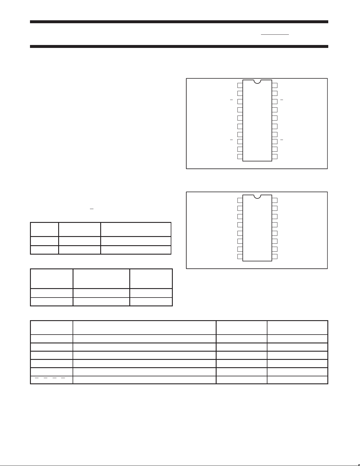
PIN CONFIGURATION – 74F398
S
1
Qa
2
a
Q
3
I0a
4
I1a
5
I1b
6
I0b
PIN CONFIGURATION – 74F399
S
1
Qa
2
I0a
3
I1a
4
I1b
5
I0b
20
19
18
17
16
15
147
138QbQc
129Qb Qc
1110GND CP
SF00947
16
15
14
13
12
116
107Qb Qc
98GND CP
SF00951
V
Qd
Q
I0d
I1d
I1c
I0c
V
Qd
I0d
I1d
I1c
I0c
CC
d
CC
INPUT AND OUTPUT LOADING AND FAN-OUT TABLE
PINS DESCRIPTION
74F (U.L.)
HIGH/LOW
I0a, I0b, I0c, I0d Data inputs from source 0 1.0/1.0 20µA/0.6mA
I1a, I1b, I1c, I1d Data inputs from source 1 1.0/1.0 20µA/0.6mA
S Common Select input 1.0/1.0 20µA/0.6mA
CP Clock input (active rising edge) 1.0/1.0 20µA/0.6mA
Qa, Qb, Qc, Qd Register true outputs 50/33 1.0mA/20mA
Qa, Qb, Qc, Qd Register complementary outputs (74F398) 50/33 1.0mA/20mA
NOTE:
One (1.0) FAST unit load is defined as: 20µA in the High state and 0.6mA in the Low state.
* Discontinued part. Please see the Discontinued Products List..
1999 Jan 08 853–0028 20616
2
LOAD VALUE
HIGH/LOW
Philips Semiconductors Product specification
74F398*,74F399Registers
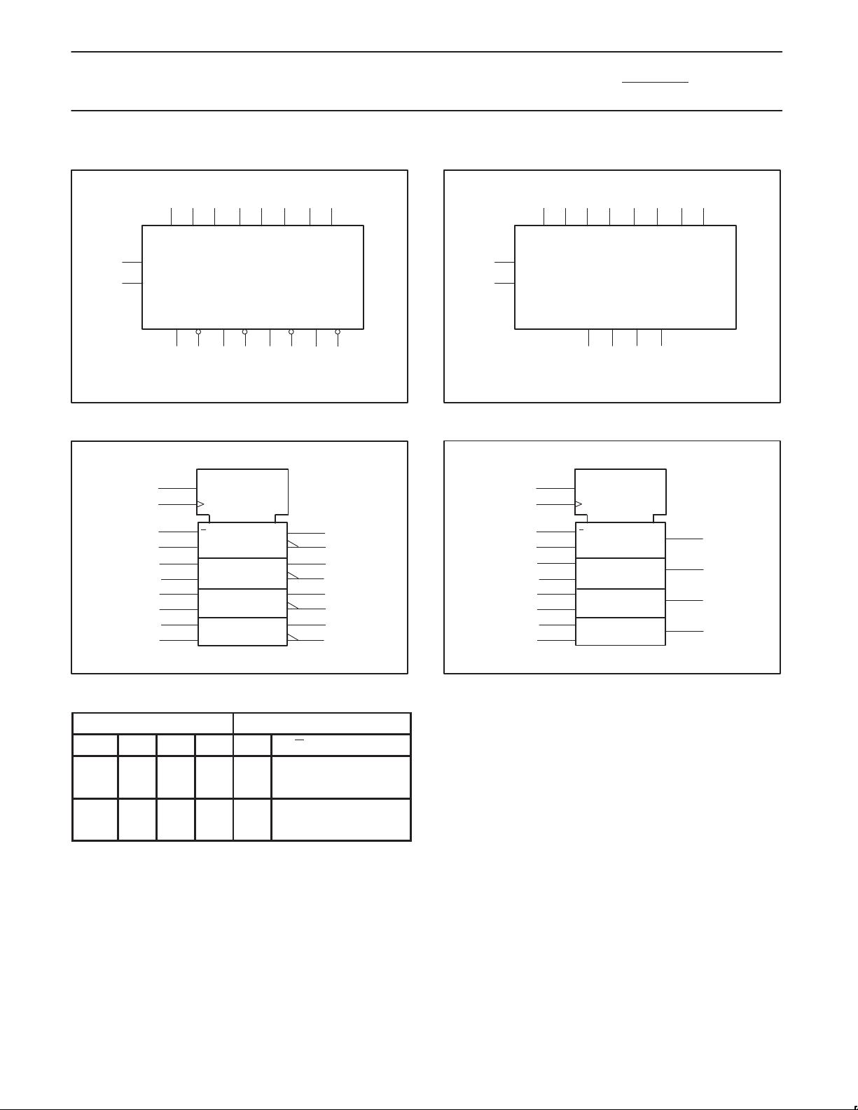
LOGIC SYMBOL – 74F398
57614
1
11
VCC= Pin 20
GND = Pin 10
4
I1a I0b I1b I0c
I0a
S
CP
Qa Qa Qb Qb
2398
15 17 16
I1c I0d I1d
Qc Qc Qd Qd
12 13 19 18
IEC/IEEE SYMBOL (IEEE/IEC) – 74F398
G1
C2
, 2D
1
1, 2D
MUX
2
3
9
8
12
13
19
18
1
11
4
5
7
6
14
15
17
16
SF00948
LOGIC SYMBOL – 74F399
46511
1
9
VCC= Pin 16
GND = Pin 8
3
I0a
S
CP
I1a I0b I1b I0c
Qa Qb
27
12 14 13
I1c I0d I1d
Qc Qd
10 15
IEC/IEEE SYMBOL (IEEE/IEC) – 74F399
G1
C1
1
, 2D
1, 2D
MUX
1
9
3
4
6
5
11
12
14
13
SF00952
2
7
10
15
SF00949
FUNCTION TABLE
INPUTS OUTPUTS
CP S I0n I1n Qn Qn (74F398 only)
H = High voltage level
h = High voltage level one setup time prior to the High-to-Low
L = Low voltage level
l = Low voltage level one setup time prior to the High-to-Low
X = Don’t care
= Low-to-High clock transition
* Discontinued part. Please see the Discontinued Products List..
1999 Jan 08
l l X L H
l h X H L
h X l L H
h X h H L
clock transition
clock transition
SF00953
3
 Loading...