

Philips N74F393N, N74F393D Datasheet

INTEGRATED CIRCUITS
74F393
Dual 4-bit binary ripple counter
Product specification
IC15 Data Handbook
1988 Nov 01
Philips Semiconductors Product specification
74F393Dual 4-bit binary ripple counter
FEA TURES
•Two 4-bit binary counters
•Two Master Resets to clear each 4-bit counter individually
DESCRIPTION
The 74F393 is a Dual Ripple Counter with separate Clock (CPn) and
Master Reset (MR) inputs to each counter. The two counters are
identified by the “a” and “b” suffixes in the pin configuration. The
operation of each half of the 74F393 is the same. The counters are
triggered by a High-to-Low transition of the Clock (CP
inputs. The counter outputs are internally connected to provide
Clock inputs to succeeding stages. The outputs of the ripple counter
do not change synchronously and should not be used for high speed
address decoding. The Master Resets (MR
and MRb) are active
a
High asynchronous inputs; one for each 4-bit counter. A High level
in the MR input overrides the Clock and sets the outputs Low.
and CPb)
a
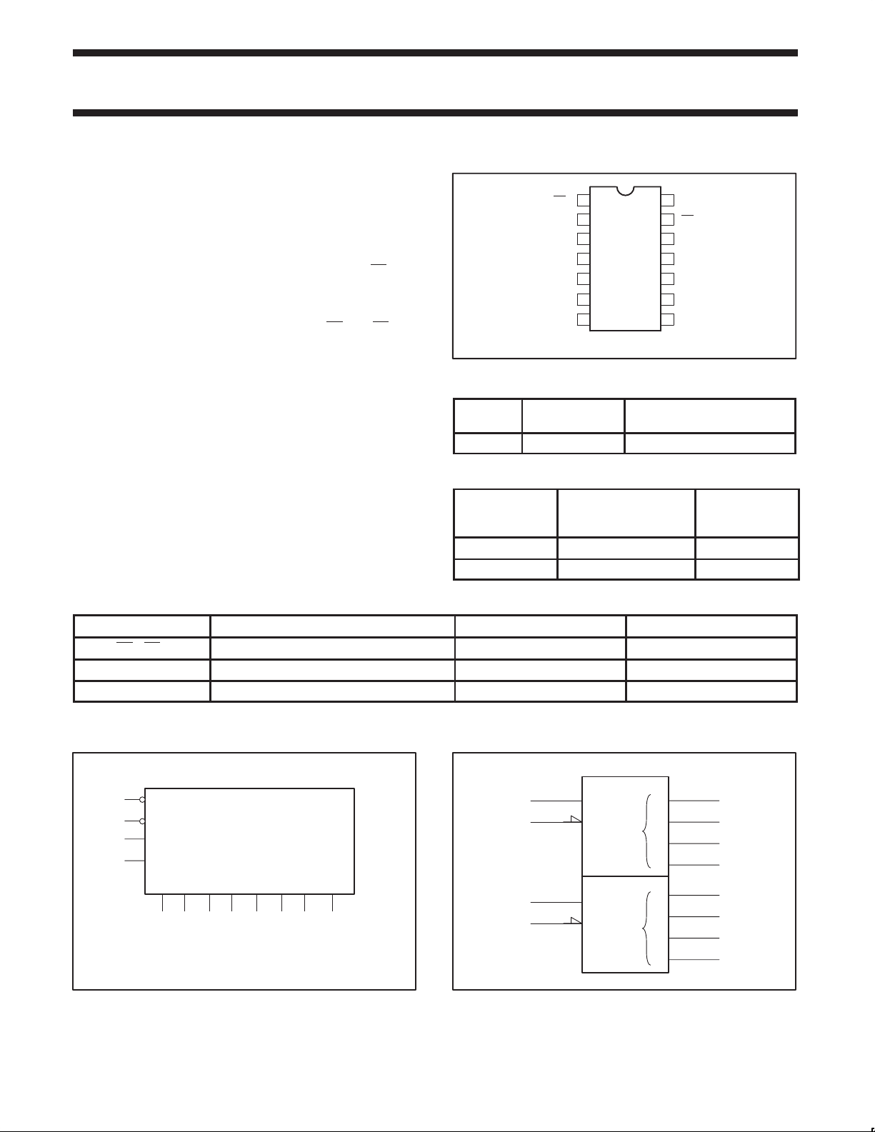
PIN CONFIGURATION
1
a
CP
2
MRa
3
Q0a
4
Q1a
5
Q2a
6
Q3a
GND
TYPE TYPICAL f
MAX
74F393 125MHz 40mA
14
V
CC
CP
b
13
MRb
12
Q0b
11
Q1b
10
Q2b
9
Q3b
87
SF00704
TYPICAL SUPPL Y CURRENT
(TOTAL)
ORDERING INFORMATION
COMMERCIAL RANGE
DESCRIPTION
14-pin plastic DIP N74F393N SOT27-1
14-pin plastic SO N74F393D SOT108-1
VCC = 5V ±10%,
T
= 0°C to +70°C
amb
PKG DWG #
INPUT AND OUTPUT LOADING AND FAN-OUT TABLE
PINS DESCRIPTION 74F (U.L.) HIGH/LOW LOAD VALUE HIGH/LOW
CPa, CP
MRa, MR
Qna – Q
b
b
nb
NOTE: One (1.0) FAST unit load is defined as: 20µA in the High state and 0.6mA in the Low state.
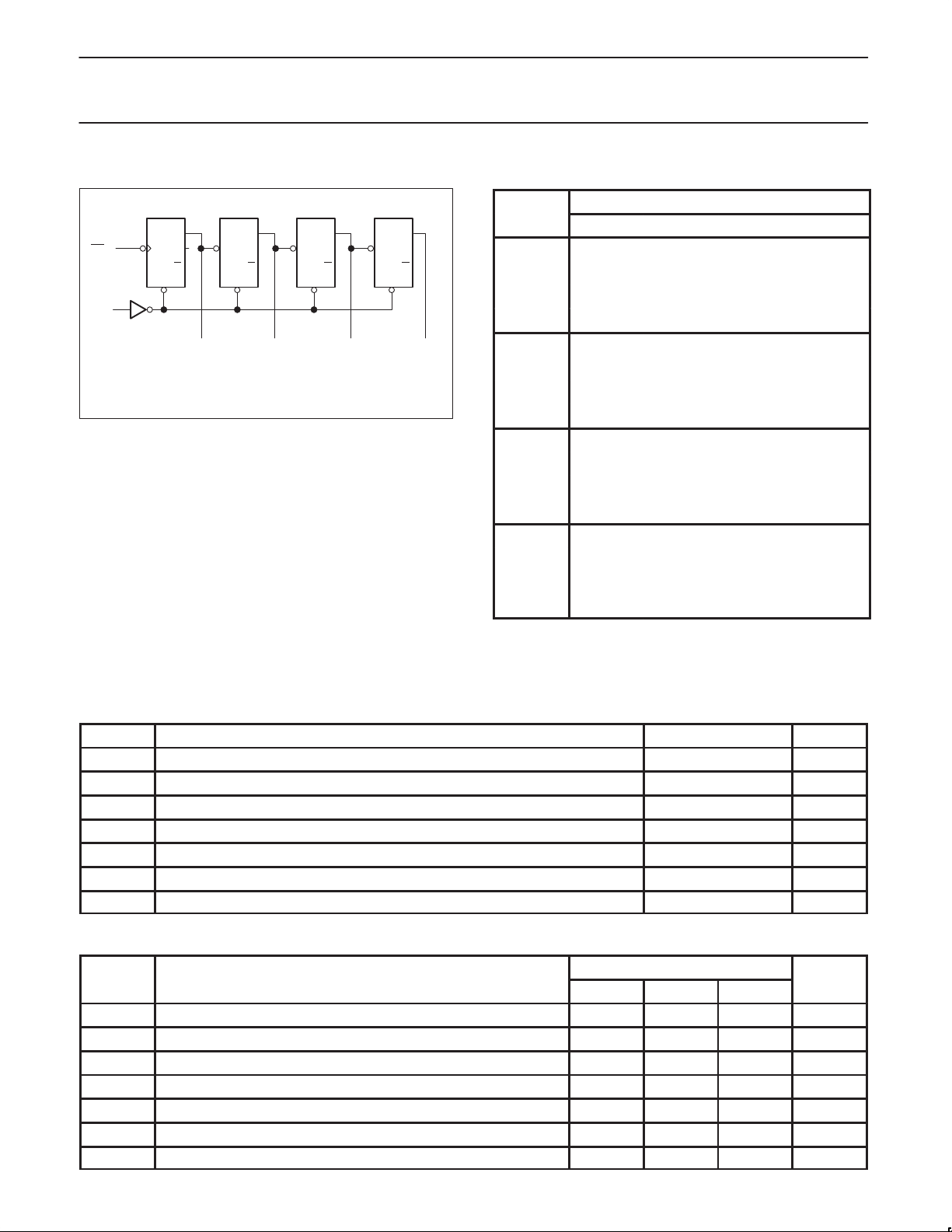
LOGIC SYMBOL
CP
1
13
2
12
VCC= Pin 14
GND = Pin 7
a
CP
b
MR
a
MR
b
Q0a Q1a Q2a Q3a Q0b Q1b Q2b Q3b
345611109 8
Clock inputs 1.0/1.0 20µA/0.6mA
Master Reset inputs 1.0/1.0 20µA/0.6mA
Data outputs 50/33.3 1.0mA/20mA
IEC/IEEE SYMBOL (IEEE/IEC)
2
1
12
13
SF00705
CTR DIV 16
CT=0
+
CTR DIV 16
CT=0
+
0
3
0
3
3
4
5
6
11
10
9
8
SF00706
1988 Nov 01 853–0295 94977
2
Philips Semiconductors Product specification
COUNT
SYMBOL
PARAMETER
UNIT
74F393Dual 4-bit binary ripple counter
LOGIC DIAGRAM
Q
J
1, 13
CPn
2, 12
MRn
VCC = Pin 14
GND = Pin 7
CP
R
D
Q0n
3, 11
FUNCTION TABLE
OUTPUTS
Q
Q
J
CP
KQKQKQK
Q
R
D
Q
J
CP
R
D
Q
J
CP
R
D
0 L L L L
1 H LLL
0n
2 L HLL
3 H HLL
4 L L H L
Q1n
4, 10
Q2n
5, 9
6, 8
Q3n
5 H LHL
6 L HHL
SF00707
7 H HHL
8 L L L H
9 H LLH
10 L HLH
11 H HLH
12 L L H H
13 H LHH
14 L HHH
15 H H H H
H = High voltage level transition
L = Low voltage level
Q
1n
Q
2n
Q
3n
ABSOLUTE MAXIMUM RATINGS
(Operation beyond the limits set forth in this table may impair the useful life of the device.
Unless otherwise noted these limits are over the operating free-air temperature range.)
SYMBOL
V
CC
V
IN
I
IN
V
OUT
I
OUT
T
amb
T
stg
Supply voltage –0.5 to +7.0 V
Input voltage –0.5 to +7.0 V
Input current –30 to +5 mA
Voltage applied to output in High output state –0.5 to V
Current applied to output in Low output state 40 mA
Operating free-air temperature range 0 to +70 °C
Storage temperature range –65 to +150 °C
PARAMETER RATING UNIT
RECOMMENDED OPERATING CONDITIONS
V
V
V
I
I
I
T
CC
IH
IL
IK
OH
OL
amb
Supply voltage 4.5 5.0 5.5 V
High-level input voltage 2.0 V
Low-level input voltage 0.8 V
Input clamp current –18 mA
High-level output current –1 mA
Low-level output current 20 mA
Operating free-air temperature range 0 70 °C
CC
LIMITS
MIN NOM MAX
V
1988 Nov 01
3
 Loading...