Philips N74F377AD, N74F377AN Datasheet

INTEGRATED CIRCUITS
74F377A
Octal D-type flip-flop with enable
Product specification
IC15 Data Handbook
1996 Mar 12

Philips Semiconductors Product specification
74F377AOctal D-type flip-flop with enable
FEA TURES
•High impedance inputs for reduced loading (20µA in Low and
High states)
•Ideal for addressable register applications
•Enable for address and data synchronization applications
•Eight edge–triggered D–type flip–flops
•Buffered common clock
•See ’F273A for Master Reset version
DESCRIPTION
The 74F377A has 8 edge-triggered D-type flip-flops with individual D
inputs and Q outputs. The common buffered clock (CP) input loads
all flip-flops simultaneously when the Enable (E
The register is fully edge triggered. The state of each D input, one
set-up time before the Low-to-High clock transition, is transferred to
the corresponding flip-flop’s Q output.
The E
input must be stable one setup time prior to the Low-to-High
clock transition for predictable operation.
•See ’F373 for transparent latch version
•See ’F374 for 3–State version
TYPE
74F377A 165MHz 29mA
ORDERING INFORMATION
PACKAGES
20–pin plastic DIP N74F377AN SOT146-1
20–pin plastic SOL N74F377AD SOT163-1
TYPICAL f
MAX
COMMERCIAL RANGE
VCC = 5V±10%; T
TYPICAL SUPPLY CURRENT (TOTAL)
= 0°C to +70°C
amb
) input is Low.
PKG. DWG. #
INPUT AND OUTPUT LOADING AND FAN–OUT TABLE
PINS DESCRIPTION
D0 – D7 Data inputs 1.0/0.033 20µA/20µA
CP Clock pulse input (active rising edge) 1.0/0.033 20µA/20µA
E Enable input (active–Low) 1.0/0.033 20µA/20µA
Q0 – Q7 Data outputs 50/33 1.0mA/20mA
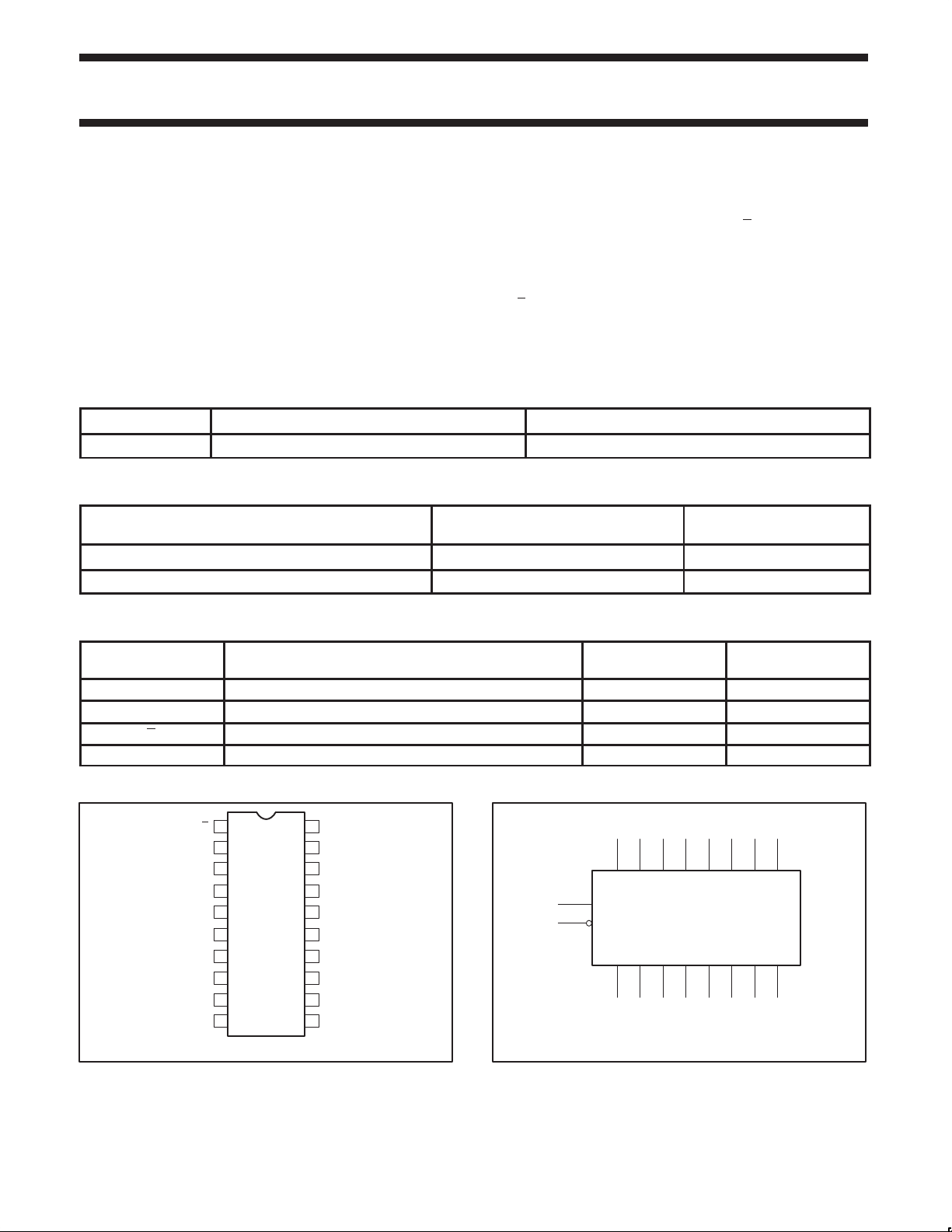
PIN CONFIGURATION
V
1
E
2
Q0
3
D0
4
D1
5
Q1
6
Q2
7
D2
8
D3
9
Q3
10 11
GND
20
19
18
17
16
15
14
13
12
SF00350
CC
Q7
D7
D6
Q6
Q5
D5
D4
Q4
CP
LOGIC SYMBOL
11
1
V
= Pin 20
CC
GND = Pin 10
CP
E
74F(U.L.)
HIGH/LOW
3 4 7 8 13 14 1817
D0 D1 D2 D3 D4 D5 D6 D7
Q0 Q1 Q2 Q3 Q4 Q5 Q6 Q7
2 5 6 9 12 15 16 19
LOAD VALUE
HIGH/LOW
SF00351
1996 Mar 12 853–0026 16555
2

Philips Semiconductors Product specification
74F377AOctal D-type flip-flop with enable
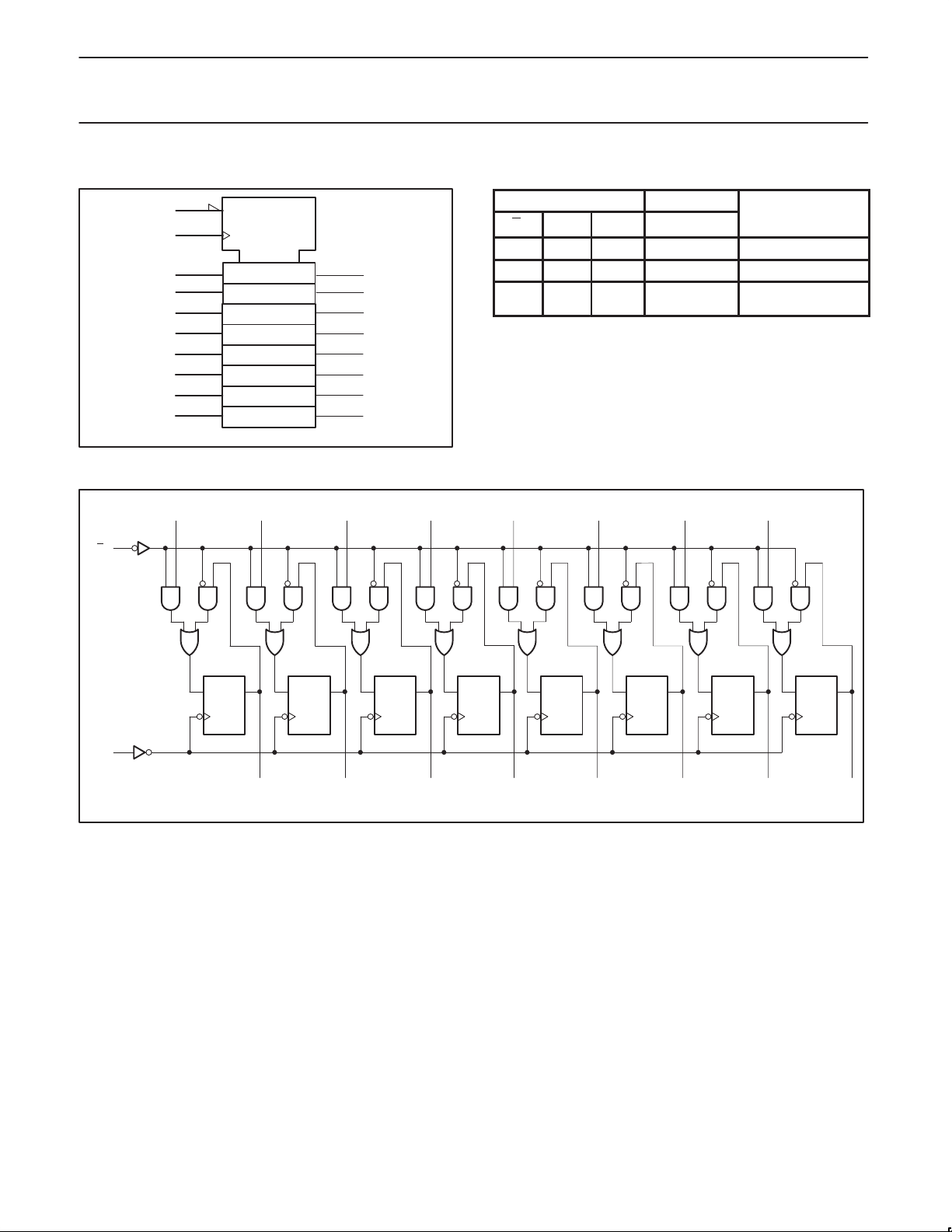
LOGIC SYMBOL (IEEE/IEC)
1
G1
11
32
4
7
8
13
14
17
18
1C2
2D
LOGIC DIAGRAM
D0 D1 D2 D3
1
E
3478
12
15
16
19
SF00352
FUNCTION TABLE
INPUTS OUTPUTS OPERATING MODE
E CP Dn Qn
l ↑ h H Load “1”
5
6
9
l ↑ l L Load “0”
h
H
↑
X
X
X
no change
no change
Hold (do nothing)
H = High voltage level
h = High voltage level one set-up time prior to the Low-to-High
clock transition
L = Low voltage level
l = Low voltage level one set-up time prior to the Low-to-High
clock transition
X = Don’t care
↑ = Low-to-High clock transition
D4 D5 D6 D7
13 14 17 18
11
CP
VCC = Pin 20
GND = Pin 10
DQ
CP
D
CP
2 5 6 9 12 15 16 19
Q0 Q1 Q2 Q3
D
QQ
CP
DQ
CP
DQ
CP
D
CP
Q4 Q5 Q6 Q7
D
QQ
CP
DQ
CP
SF00353
1996 Mar 12
3
 Loading...