

Philips N74F374DB, N74F374D, N74F373DB, N74F373D, N74F374N Datasheet
...
Philips Semiconductors
74F373
Octal transparent latch (3-State)
74F374
Octal D flip-flop (3-State)
Product specification 1994 Dec 05
FAST PRODUCTS
IC15 Data Handbook

Philips Semiconductors Product specification
74F373/74F374Latch/flip-flop
74F373 Octal transparent latch (3-State)
74F374 Octal D-type flip-flop (3-State)
2
December 5, 1994 853-0369 14383
FEA TURES
•8-bit transparent latch — 74F373
•8-bit positive edge triggered register — 74F374
•3-State outputs glitch free during power-up and power-down
•Common 3-State output register
•Independent register and 3-State buffer operation
•SSOP Type II Package
DESCRIPTION
The 74F373 is an octal transparent latch coupled to eight 3-State
output devices. The two sections of the device are controlled
independently by enable (E) and output enable (OE
) control gates.
The data on the D inputs is transferred to the latch outputs when the
enable (E) input is high. The latch remains transparent to the data
input while E is high, and stores the data that is present one setup
time before the high-to-low enable transition.
The 3-State output buffers are designed to drive heavily loaded
3-State buses, MOS memories, or MOS microprocessors.
The active low output enable (OE
) controls all eight 3-State buffers
independent of the latch operation. When OE
is low, latched or
transparent data appears at the output.
When OE
is high, the outputs are in high impedance “off” state,
which means they will neither drive nor load the bus.
The 74F374 is an 8-bit edge triggered register coupled to eight
3-State output buffers. The two sections of the device are controlled
independently by clock (CP) and output enable (OE
) control gates.
The register is fully edge triggered. The state of the D input, one
setup time before the low-to-high clock transition is transferred to the
corresponding flip-flop’s Q output.
The 3-State output buffers are designed to drive heavily loaded
3-State buses, MOS memories, or MOS microprocessors.
The active low output enable (OE
) controls all eight 3-State buffers
independent of the register operation. When OE
is low, the data in
the register appears at the outputs. When OE
is high, the outputs
are in high impedance “off” state, which means they will neither drive
nor load the bus.
TYPE
TYPICAL
PROPAGATION
DELA Y
TYPICAL SUPPL Y
CURRENT
(TOT AL)
74F373 4.5ns 35mA
TYPE TYPICAL f
max
TYPICAL SUPPL Y
CURRENT
(TOT AL)
74F374 165MHz 55mA
ORDERING INFORMATION
ORDER CODE
DESCRIPTION COMMERCIAL RANGE PKG DWG #
VCC = 5V ±10%, T
amb
= 0°C to +70°C
20-pin plastic DIP N74F373N, N74F374N SOT146-1
20-pin plastic SOL N74F373D, N74F374D SOT163-1
20-pin plastic SSOP type II N74F373DB, N74374DB SOT399-1
INPUT AND OUTPUT LOADING AND FAN OUT TABLE
PINS DESCRIPTION
74F (U.L.)
HIGH/LOW
LOAD VALUE
HIGH/LOW
D0 - D7 Data inputs 1.0/1.0
20µA/0.6mA
E (74F373) Enable input (active high) 1.0/1.0
20µA/0.6mA
OE Output enable inputs (active low) 1.0/1.0
20µA/0.6mA
CP (74F374) Clock pulse input (active rising edge) 1.0/1.0
20µA/0.6mA
Q0 - Q7 3-State outputs 150/40 3.0mA/24mA
NOTE: One (1.0) FAST unit load is defined as: 20µA in the high state and 0.6mA in the low state.

Philips Semiconductors Product specification
74F373/74F374Latch/flip-flop
December 5, 1994
3
PIN CONFIGURATION – 74F373
1
2
3
4
5
6
7
8
9
10 11
12
13
14
15
16
17
18
19
20
OE
Q0
D0
D1
Q1
Q2
D2
D3
Q3
GND
V
CC
Q7
D7
D6
Q6
Q5
D5
D4
Q4
E
SF00250
LOGIC SYMBOL – 74F373
E
Q0 Q1 Q2 Q3 Q4 Q5 Q6 Q7
D0 D1 D2 D3 D4 D5 D6 D7
3 4 7 8 13 14 17 18
2 5 6 9 12 15 16 19
V
CC
= Pin 20
GND = Pin 10
11
1
OE
SF00251
IEC/IEEE SYMBOL – 74F373
1
EN2
2D
EN1
1
11
3
4
7
8
13
14
17
18
2
5
6
12
9
15
16
19
SF00252
PIN CONFIGURATION – 74F374
1
2
3
4
5
6
7
8
9
10 11
12
13
14
15
16
17
18
19
20
OE
Q0
D0
D1
Q1
Q2
D2
D3
Q3
GND
V
CC
Q7
D7
D6
Q6
Q5
D5
D4
Q4
CP
SF00253
IEC/IEE SYMBOL – 74F374
CP
Q0 Q1 Q2 Q3 Q4 Q5 Q6 Q7
D0 D1 D2 D3 D4 D5 D6 D7
3 4 7 8 13 14 17 18
2 5 6 9 12 15 16 19
V
CC
= Pin 20
11
1
GND = Pin 10
OE
SF00254
IEC/IEEE SYMBOL – 74F374
1
C2
2D
EN1
1
11
3
4
7
8
13
14
17
18
2
5
6
9
12
15
16
19
SF00255
Philips Semiconductors Product specification
74F373/74F374Latch/flip-flop
December 5, 1994
4
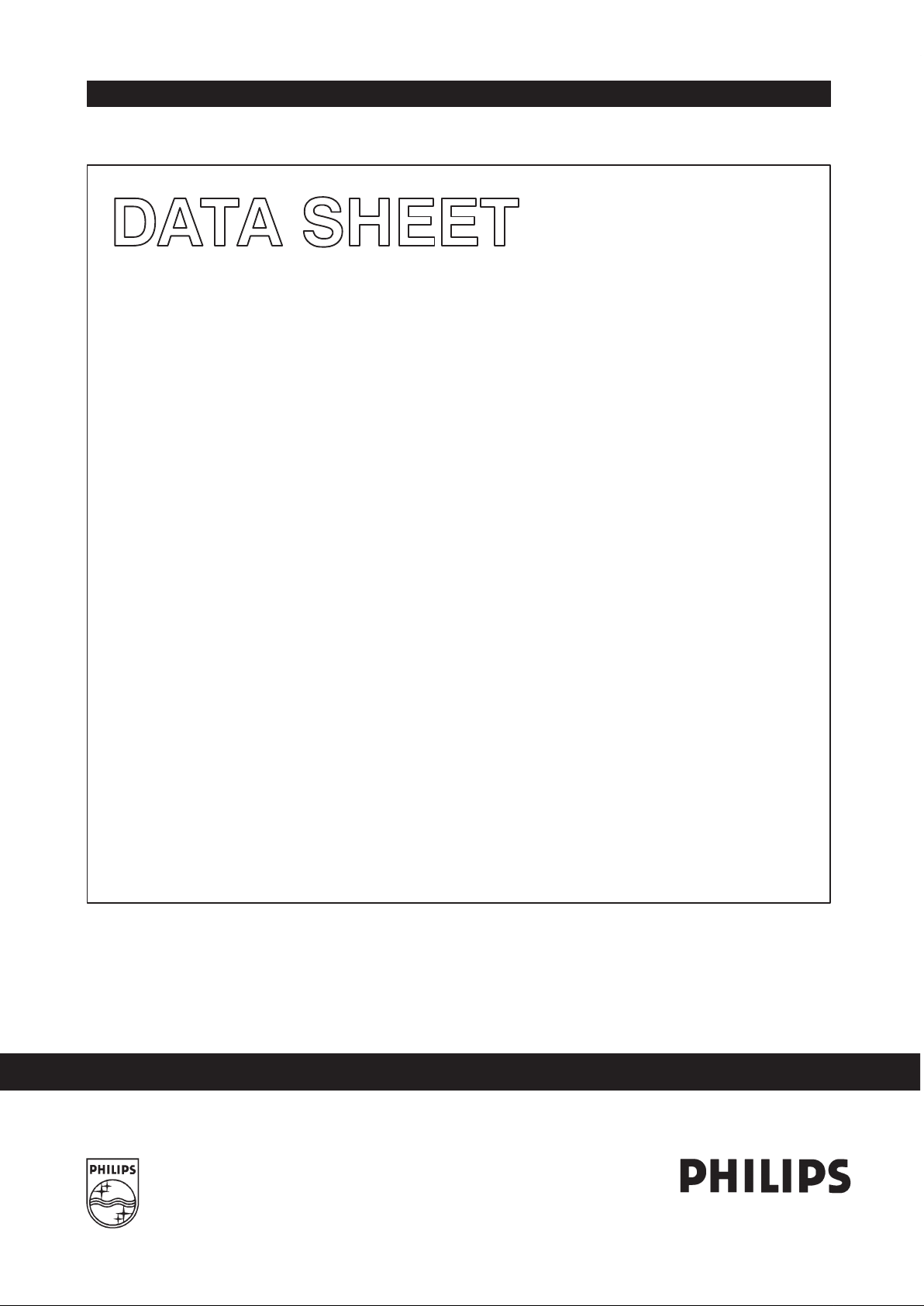
LOGIC DIAGRAM FOR 74F373
V
CC
= Pin 20
GND = Pin 10
D0
D
E
Q
Q0
3
2
D1
D
E
Q
Q1
4
5
D2
D
E
Q
Q2
7
6
D3
D
E
Q
Q3
8
9
D4
D
E
Q
Q4
13
12
D5
D
E
Q
Q5
14
15
D6
D
E
Q
Q6
17
16
D7
D
E
Q
Q7
18
19
11
1
E
OE
SF00256
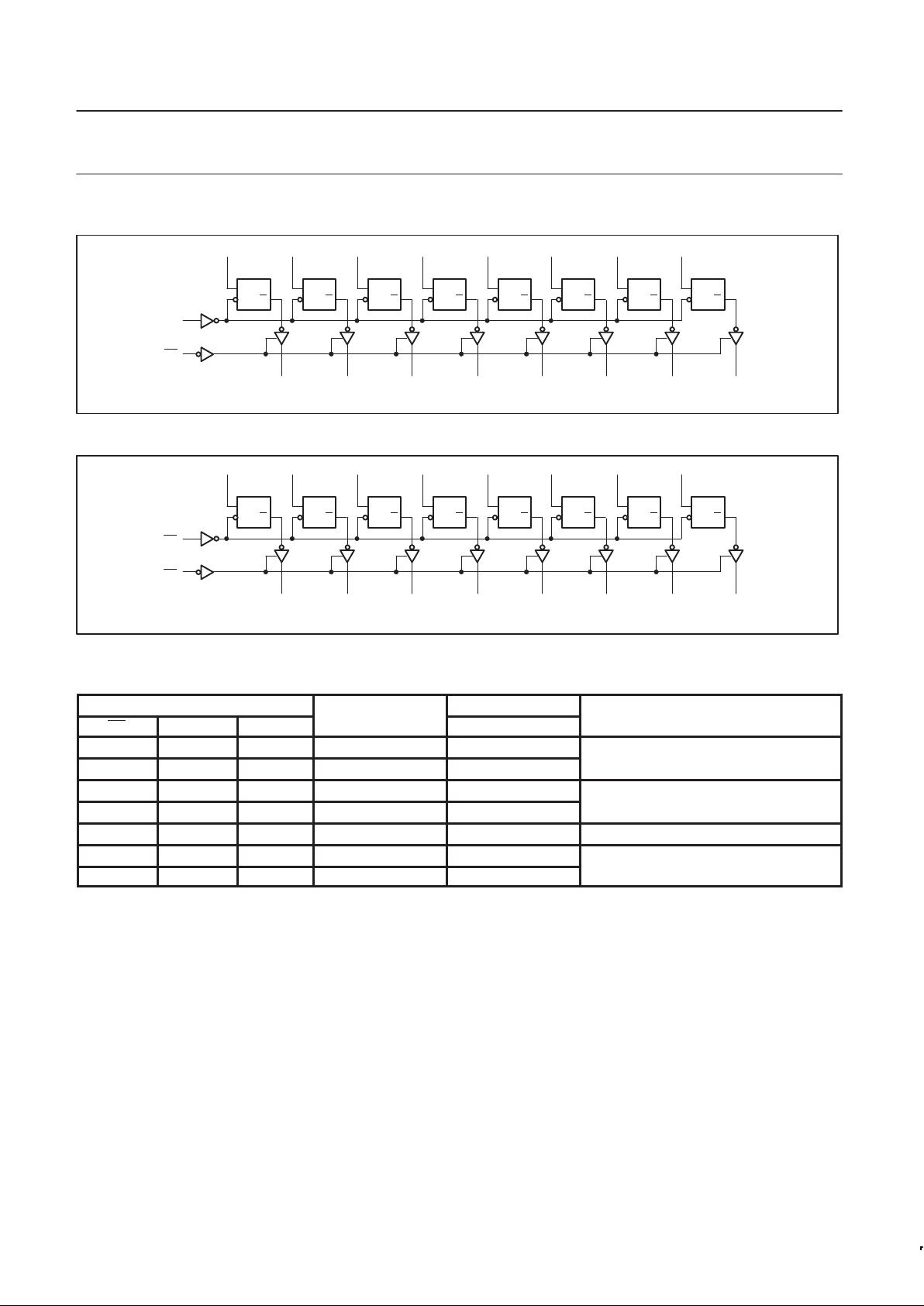
LOGIC DIAGRAM FOR 74F374
VCC = Pin 20
D0
D
CP
Q
Q0
3
2
D1
D
CP
Q
Q1
4
5
D2
D
CP
Q
Q2
7
6
D3
D
CP
Q
Q3
8
9
D4
D
CP
Q
Q4
13
12
D5
D
CP
Q
Q5
14
15
D6
D
CP
Q
Q6
17
16
D7
D
CP
Q
Q7
18
19
11
1
OE
CP
GND = Pin 10
SF00257
FUNCTION TABLE FOR 74F373
INPUTS
INTERNAL
OUTPUTS
OE E Dn
REGISTER
Q0 - Q7
OPERATING MODE
L H L L L
L H H H H
Enable and read register
L ↓ l L L
L ↓ h H H
Latch and read register
L L X NC NC Hold
H L X NC Z
p
H H Dn Dn Z
Disable outputs
NOTES:
H = High-voltage level
h = High state must be present one setup time before the high-to-low enable transition
L = Low-voltage level
l = Low state must be present one setup time before the high-to-low enable transition
NC= No change
X = Don’t care
Z = High impedance “off” state
↓ = High-to-low enable transition
 Loading...