

Philips N74F3037N, N74F3037D Datasheet
INTEGRATED CIRCUITS
74F3037
Quad 2-input NAND 30Ω driver
Product specification
IC15 Data Handbook
1990 Feb 09
Philips Semiconductors Product specification
74F3037Quad 2-input NAND 30Ω driver
FEA TURES
• 30Ω line driver
• 67mA output drive capability in the high state
• High speed
• Facilitates incident wave switching
• 3nh lead inductance each on V
side pins are used
and GND when both
CC
• 160mA output drive capability in the low state
• Industrial temperature range available (–40°C to +85°C)
transmission line effects of PC boards which appear when
fast edge rates are used.
The drive capability of the 74F3037 is 67mA source and
160mA sink with a V
incident wave switching with V
as low as 4.5V. This guarantees
CC
not less than 2.0V and V
OH
not more than 0.8mA while driving impedances as low as 30
ohms. This is applicable with any combination of outputs
using continuous duty . The propagation delay of the part is
minimally affected by reflections when terminated only by
the TTL inputs of other devices. Performances may be
improved by full or partial line termination.
DESCRIPTION
The 74F3037 is a high current line driver composed of four
2–input NAND gates. It has been designed to deal with the
TYPE TYPICAL
PROPAGATION DELAY
74F3037 2.0ns 16mA
TYPICAL SUPPL Y
CURRENT( TOTAL)
ORDERING INFORMATION
ORDER CODE
COMMERCIAL RANGE INDUSTRIAL RANGE
DESCRIPTION
16–pin plastic DIP N74F3037N I74F3037N SOT38-4
16–pin plastic SOL N74F3037D I74F3037D SOT162-1
VCC = 5V ±10%, VCC = 5V ±10%,
T
= 0°C to +70°C T
amb
= –40°C to +85°C
amb
PKG DWG #
OL
INPUT AND OUTPUT LOADING AND FAN OUT TABLE
PINS DESCRIPTION 74F (U.L.) HIGH/LOW LOAD VALUE HIGH/LOW
Dna, Dnb Data inputs 1.0/1.0
Qn Data output 3350/266 67mA/160mA
Note to input and output loading and fan out table
One (1.0) FAST unit load is defined as: 20
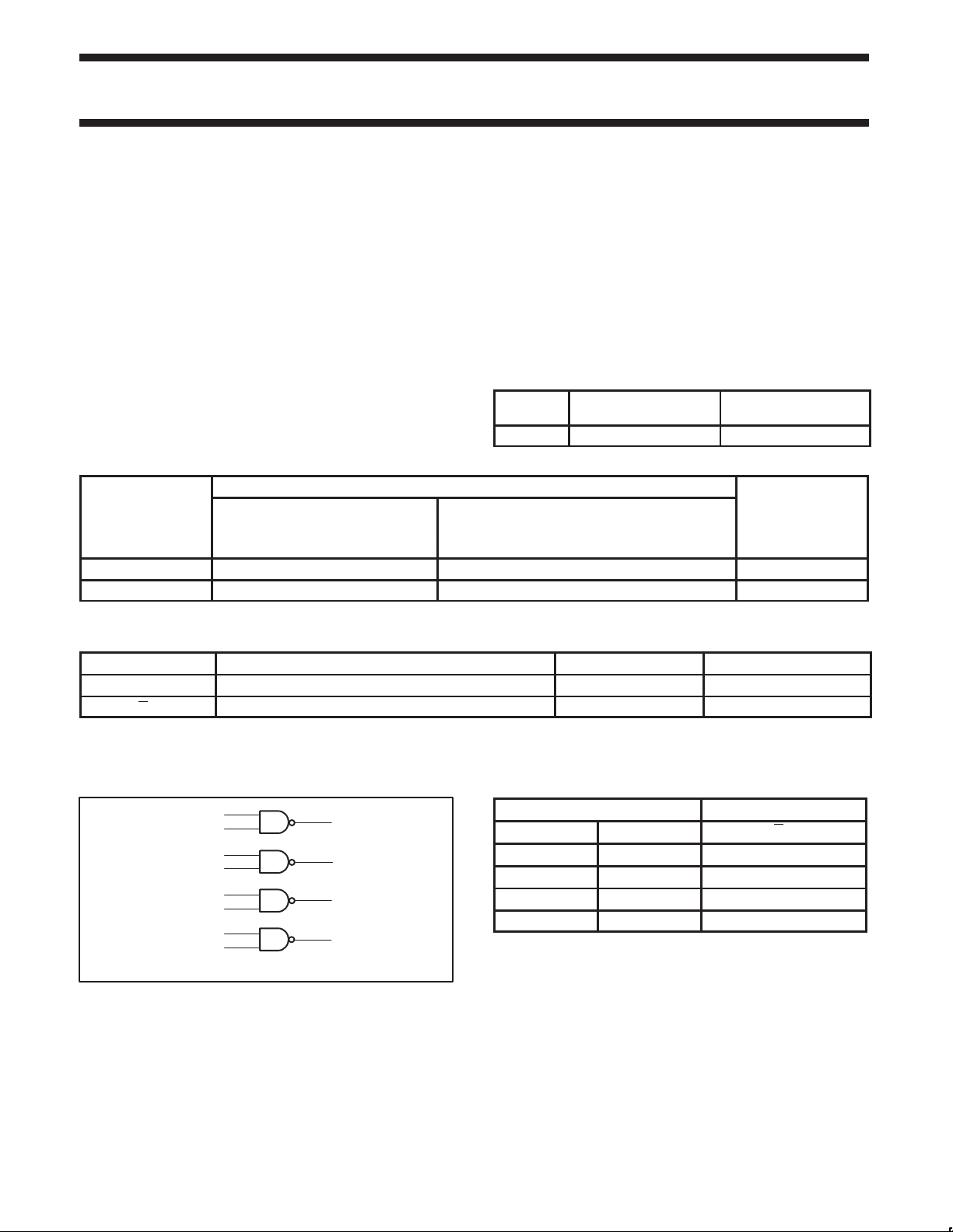
LOGIC DIAGRAM
1
D0a
2
D0b
7
D1a
8
D1b
10
D2a
11
D2b
14
D3a
15
VCC = Pin 12,13
GND = Pin 4, 5
D3b
µA in the high state and 0.6mA in the low state.
FUNCTION TABLE
3
6
9
16
SF00569
Q0
Q1
Q2
Q3
Dna Dnb Qn
L L H
L H H
H L H
H H L
Notes to function table
H = High voltage level
L = Low voltage level
20µA/0.6mA
INPUTS OUTPUT
February 9, 1990 853 0021 98744
2
Philips Semiconductors Product specification
74F3037Quad 2-input NAND 30Ω driver
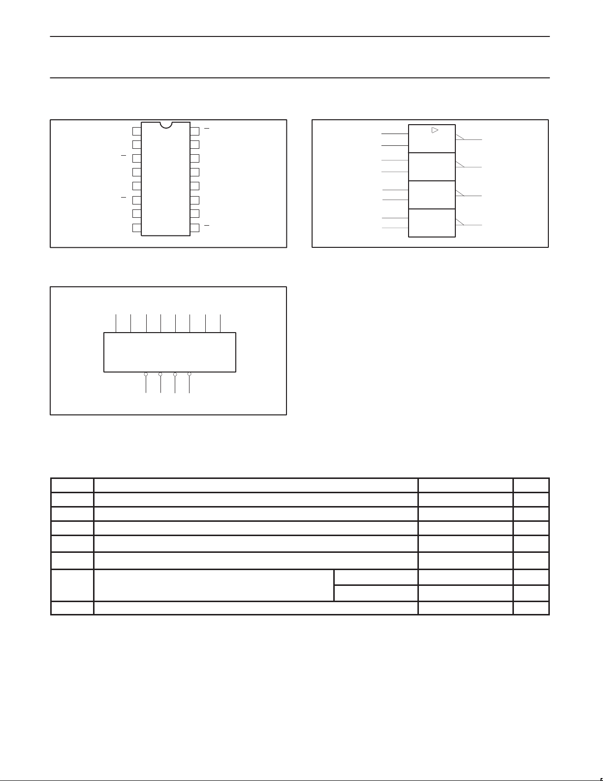
PIN CONFIGURATION
1
D0a
2
D0b
3
Q0
4
GND
5
GND
1
6
Q
D1a
8
D1b
LOGIC SYMBOL
1 2 7 8 10 11 14 15
D0b D1a D2a D2b D3a D3b
D0a
Q0 Q1 Q2 Q3
VCC = Pin 12,13
GND = Pin 4, 5
16
15
14
13
12
11
107
9
SF00570
D1a
36916
Q3
D3b
D3a
V
CC
V
CC
D2a
D2b
2
Q
SF00571
IEC/IEEE SYMBOL
1
2
7
8
10
11
14
15
&
3
6
9
16
SF00572
ABSOLUTE MAXIMUM RA TINGS
(Operation beyond the limit set forth in this table may impair the useful life of the device. Unless otherwise noted these limits are over the
operating free air temperature range.)
SYMBOL
V
CC
V
IN
I
IN
V
OUT
I
OUT
T
amb
T
stg
Supply voltage –0.5 to +7.0 V
Input voltage –0.5 to +7.0 V
Input current –30 to +5 mA
Voltage applied to output in high output state –0.5 to V
Current applied to output in low output state 320 mA
Operating free air temperature range Commercial range 0 to +70
Storage temperature range –65 to +150
PARAMETER RATING UNIT
CC
Industrial range –40 to +85
V
°C
°C
°C
February 9, 1990
3
 Loading...