

Philips N74F299N, N74F299DB Datasheet
INTEGRATED CIRCUITS
74F299
8-bit universal shift/storage register
(3-State)
Product specification
IC15 Data Handbook
1990 Mar 01
Philips Semiconductors Product specification
I/On
74F2998-bit universal shift/storage register (3-State)
FEA TURES
•Common parallel I/O for reduced pin count
•Additional serial inputs and outputs for expansion
•Four operating modes: Shift left, shift right, load and store
•3-State outputs for bus-oriented applications
DESCRIPTION
The 74F299 is an 8-bit universal shift/storage register with 3-State
outputs. Four modes of operation are possible: Hold (store), shift
left, shift right and parallel load. The parallel load inputs and flip-flop
outputs are multiplexed to reduce the total number of package pins.
Additional outputs are provided for flip-flops Q0 and Q7 to allow
easy serial cascading. A separate active-Low Master Reset is used
to reset the register.
The 74F299 contains eight edge-triggered D-type flip-flops and the
interstage logic necessary to perform synchronous shift left, shift
right, parallel load and hold operations. The type of operation is
determined by S0 and S1, as shown in the Function Table. All
flip-flop outputs are brought out through 3-State buffers to separate
I/O pins that also serve as data inputs in the parallel load mode.
Q0 and Q7 are also brought out on other pins for expansion in serial
shifting of longer words.
A Low signal on MR
the flip-flops. All other state changes are initiated by the rising edge
of the clock. Inputs can change when the clock is in either state
provided only that the recommended setup and hold times, relative
to the rising edge of clock are observed.
A High signal on either OE
puts the I/O pins in the high impedance state. In this condition the
shift, hold, load and reset operations can still occur. The 3-State
buffers are also disabled by High signals on both S0 and S1 in
preparation for a parallel load operation.
overrides the Select and CP inputs and resets
0 or OE1 disables the 3-State buffers and
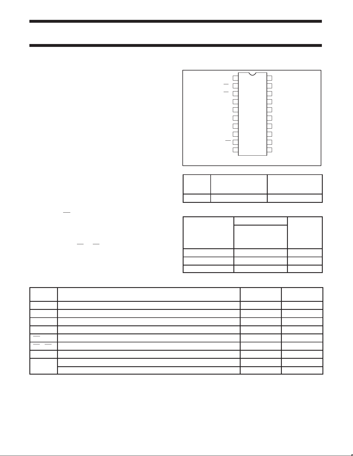
PIN CONFIGURATION
1
S0
0
2
OE
1
OE
3
4
I/O6
5
I/O4
6
I/O2
7
I/O0
8
Q0
MR
9
GND
10 11
TYPE TYPICAL f
MAX
74F299 115MHz 58mA
20
V
CC
S1
19
DS7
18
Q7
17
I/O7
16
I/O5
15
I/O3
14
I/O1
13
CP
12
DS0
SF00865
TYPICAL
SUPPLY CURRENT
(TOTAL)
ORDERING INFORMATION
ORDER CODE
DESCRIPTION
20-pin plastic DIP N74F299N SOT146-1
20-pin plastic SOL N74F299D SOT163-1
20-pin plastic SSOP II N74F299DB SOT339-1
COMMERCIAL
RANGE
= 5V ±10%,
V
CC
T
= 0°C to +70°C
amb
PKG DWG #
INPUT AND OUTPUT LOADING AND FAN-OUT TABLE
PINS DESCRIPTION
74F(U.L.)
HIGH/LOW
DS0 Serial data input for right shift 1.0/1.0 20µA/0.6mA
DS7 Serial data input for left shift 1.0/1.0 20µA/0.6mA
S0, S1 Mode select inputs 1.0/2.0 20µA/1.2mA
CP Clock pulse input (Active rising edge) 1.0/1.0 20µA/0.6mA
MR Asynchronous Master Reset input (Active Low) 1.0/1.0 20µA/0.6mA
OE0, OE1 Output Enable input (Active Low) 1.0/1.0 20µA/0.6mA
Q0, Q7 Serial outputs 50/33 1.0mA/20mA
Multiplexed parallel data inputs or 3.5/1.0 70µA/0.6mA
3-State parallel outputs 150/40 3.0mA/24mA
NOTE: One (1.0) FAST Unit Load (U.L.) is defined as: 20µA in the High State and 0.6mA in the Low state.
1990 Mar 01 853-0365 98989
2
LOAD VALUE
HIGH/LOW
Philips Semiconductors Product specification
OPERATING MODE
74F2998-bit universal shift/storage register (3-State)
LOGIC SYMBOL
1
19
12
9
2
3
V
= Pin 20
CC
GND = Pin 10
S0
S1
CP
MR
OE0
OE1
Q0 Q7
8 17
11 18
DS0 DS7
I/00 I/O2 I/O4 I/O6I/O1 I/O3 I/O5 I/O7
713614515416
SF00866
LOGIC SYMBOL (IEEE/IEC)
4R
&
0
M
1
C4/1→ /2←
1, 4D
3, 4D
5, 13
3, 4D
6, 13
3, 4D
12, 13
2, 4D
SRG8
EN13
3
0
3
9
2
3
1
19
12
11
7
13
6
14
5
15
4
16
18
Z5
Z6Z6
Z12
FUNCTION TABLE
INPUTS INPUTS
OEn MR S1 S0 CP
L L X X X Asynchronous Reset; Q0 - Q7 = Low
L H H H ↑ Parallel load; I/On → Qn (I/On outputs disabled)
L H L H ↑ Shift right; DS0 → Q0, Q0 → Q1, etc.
L H H L ↑ Shift left; DS7 → Q7, Q7 → Q6, etc.
L H L L X Hold
H X X X X Outputs in High Z
H = High voltage level
L = Low voltage level
X = Don’t care
↑ = Low-to-High clock transition
8
17
SF00890
1990 Mar 01
3
Philips Semiconductors Product specification
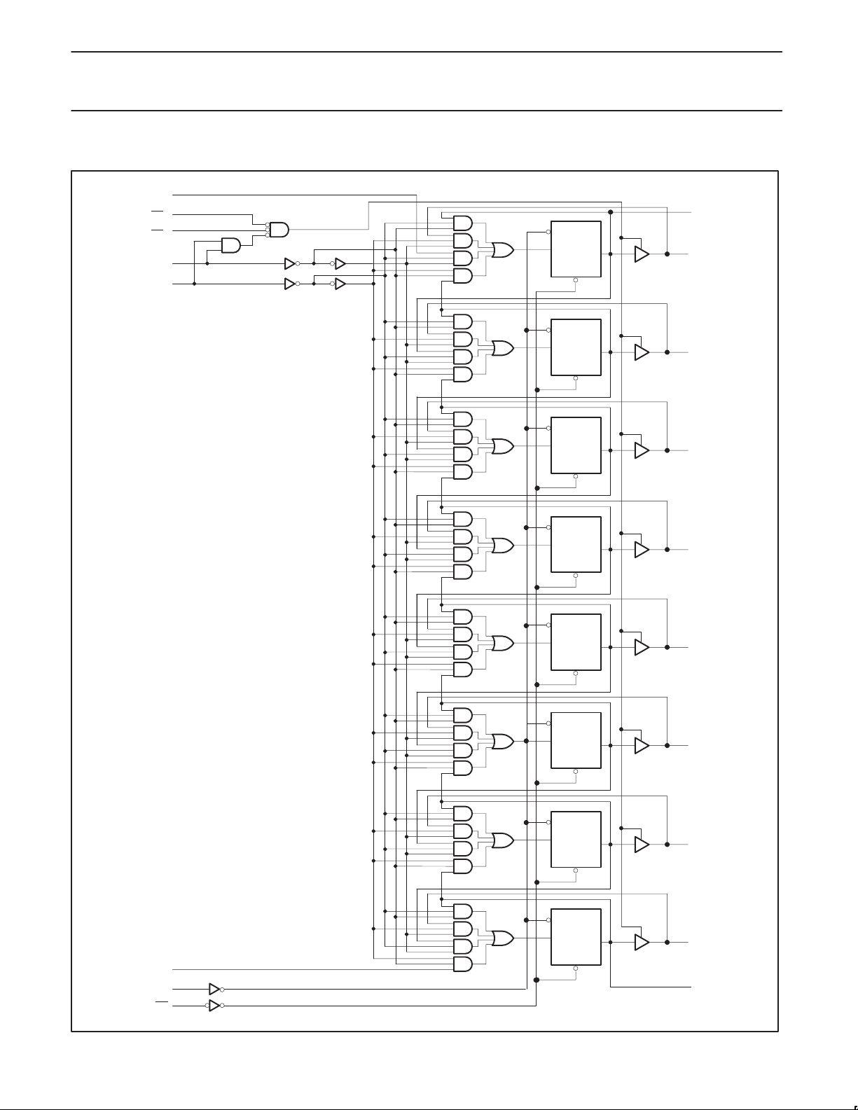
74F2998-bit universal shift/storage register (3-State)
LOGIC DIAGRAM
18
DS7
OE
OE1
2
0
3
19
S1
1
S0
CP
D
CP
D
CP
D
Q
R
D
Q
R
D
Q
R
D
17
Q7
16
I/O7
4
I/O6
15
I/O5
VCC = Pin 20
GND = Pin 10
DS0
CP
MR
CP
D
Q
R
D
CP
D
Q
R
D
CP
D
Q
R
D
CP
D
Q
R
D
CP
D
Q
R
11
12
9
D
5
I/O4
14
I/O3
6
I/O2
13
I/O1
7
I/O0
8
Q0
SF00868
1990 Mar 01
4

Philips Semiconductors Product specification
I
Current applied to output in Low output state
IOHHigh-level output current
IOLLow-level output current
74F2998-bit universal shift/storage register (3-State)
ABSOLUTE MAXIMUM RATINGS
(Operation beyond the limits set forth in this table may impair the useful life of the device. Unless otherwise noted these limits are over the
operating free-air temperature range.)
SYMBOL PARAMETER RATING UNIT
V
CC
V
IN
I
IN
V
OUT
OUT
T
amb
T
stg
RECOMMENDED OPERATING CONDITIONS
SYMBOL PARAMETER LIMITS UNIT
V
CC
V
IH
V
IL
I
IK
T
amb
Supply voltage –0.5 to +7.0 V
Input voltage –0.5 to +7.0 V
Input current –30 to +5 mA
Voltage applied to output in High output state –0.5 to +V
pp
p
p
Q0, Q7 40 mA
I/On 48 mA
CC
V
Operating free-air temperature range 0 to +70 °C
Storage temperature –65 to +150 °C
MIN NOM MAX
Supply voltage 4.5 5.0 5.5 V
High-level input voltage 2.0 V
Low-level input voltage 0.8 V
Input clamp current –18 mA
p
p
Q0, Q7 –1 mA
I/On –3 mA
Q0, Q7 20 mA
I/On 24 mA
Operating free-air temperature range 0 70 °C
1990 Mar 01
5
 Loading...