Philips N74F273AD, N74F273AN Datasheet

74F273A
Octal D flip-flop
Product specification
IC15 Data Handbook
1996 Mar 12
INTEGRATED CIRCUITS

Philips Semiconductors Product specification
74F273AOctal D flip–flop
2
1996 Mar 12 853–0066 16555
FEA TURES
• High impedance inputs for reduced loading
(20
µA in Low and High states)
• Ideal buffer for MOS microprocessor or memory
• Eight edge–triggered D–type flip–flops
• Buffered common clock
• Buffered asynchronous Master Reset
• See 74F377A for clock enable version
• See 74F373 for transparent latch version
• See 74F374 for 3–State version
DESCRIPTION
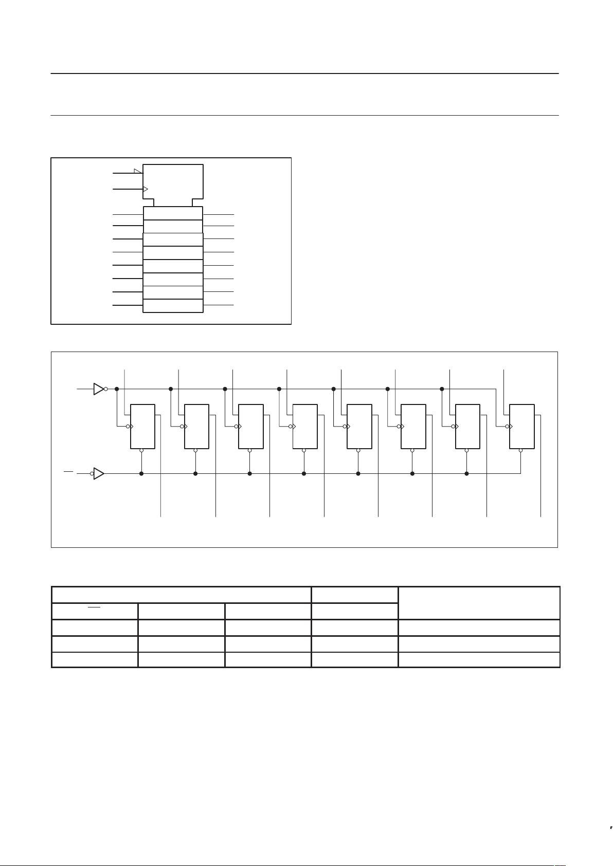
The 74F273 has eight edge–triggered D–type flip–flops with
individual D inputs and Q outputs. The common buffered Clock (CP)
and Master Reset (MR
) inputs load and reset (clear) all flip–flops
simultaneously .
The register is fully edge–triggered. The state of each D input, one
setup time before the Low–to–High clock transition, is transferred to
the corresponding flip–flop’s Q output.
All outputs will be forced Low independently of Clock or Data inputs
by a Low voltage level on the MR
input. The device is useful for
applications where the true output only is required and the CP and
MR
are common to all elements.
TYPE
TYPICAL
f
MAX
TYPICAL SUPPL Y CURRENT
(TOT AL)
74F273A 170MHz 25mA
ORDERING INFORMATION
PACKAGES
COMMERCIAL RANGE
V
CC
= 5V±10%;
T
amb
= 0°C to +70°C
PKG. DWG. #
20–pin plastic DIP 74F273AN SOT146-1
20–pin plastic SOL 74F273AD SOT163-1
INPUT AND OUTPUT LOADING AND FAN-OUT TABLE
PINS DESCRIPTION
74F(U.L.)
HIGH/LOW
LOAD VALUE
HIGH/LOW
D0 – D7 Data inputs 1.0/0.033 20µA/20µA
MR Master Reset input (active–Low) 1.0/0.033 20µA/20µA
CP Clock pulse input (active rising edge) 1.0/0.033 20µA/20µA
Q0 – Q7 Data outputs 50/33 1.0mA/20mA
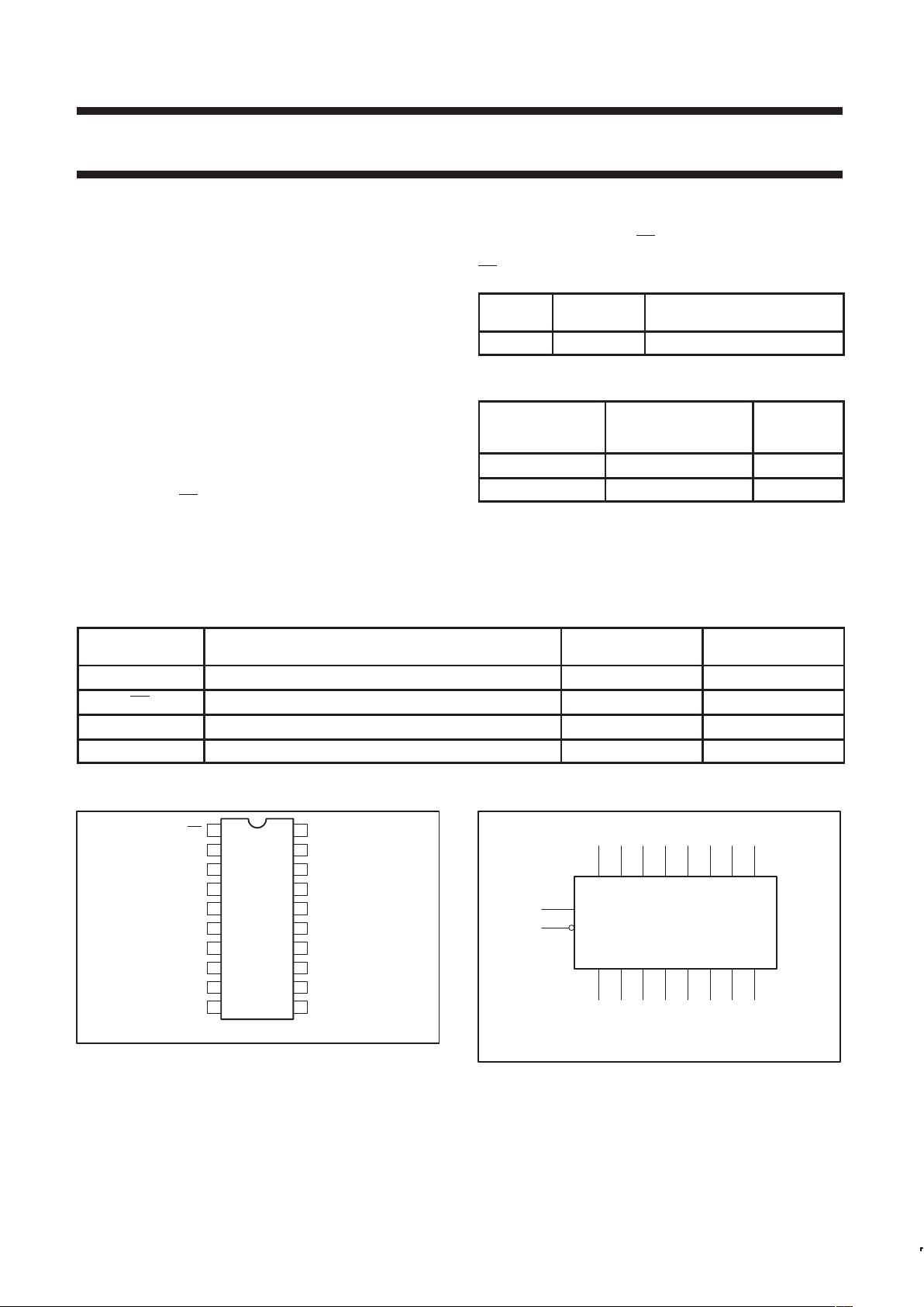
PIN CONFIGURATION
1
2
3
4
5
6
7
8
9
10 11
12
13
14
15
16
17
18
19
20
MR
Q0
D0
D1
Q1
Q2
D2
D3
Q3 Q4
GND
D4
D5
Q5
Q6
D6
D7
Q7
V
CC
CP
SF00346
LOGIC SYMBOL
3 4 7 8 13 14 1817
D0 D1 D2 D3 D4 D5 D6 D7
Q0 Q1 Q2 Q3 Q4 Q5 Q6 Q7
2 5 6 9 12 15 16 19
1
11
MR
CP
V
CC
= Pin 20
GND = Pin 10
SF00347

Philips Semiconductors Product specification
74F273AOctal D flip–flop
1996 Mar 12
3
LOGIC SYMBOL (IEEE/IEC)
SF00348
1
32
4
5
7
6
8
9
R
11
C1
13
12
14
15
17
16
18
19
1D
LOGIC DIAGRAM
CP
Q
R
D
D
3
D0
Q0
CP
Q
R
D
D
4
D1
CP
Q
R
D
D
7
D2
CP
Q
R
D
D
8
D3
CP
Q
R
D
D
13
D4
CP
Q
R
D
D
14
D5
CP
Q
R
D
D
17
D6
CP
Q
R
D
D
18
D7
2
Q1
5
Q2
6
Q3
9
Q4
12
Q5
15
Q6
16
Q7
19
11
1
CP
MR
VCC = Pin 20
GND = Pin 10
SF00349
FUNCTION TABLE
INPUTS OUTPUTS OPERATING
MR CP Dn Q0 – Q7 MODE
L X X L Reset (clear)
H ↑ h H Load ”1”
H ↑ l L Load ”0”
H = High voltage level
h = High voltage level one set–up time prior to the Low–to–High clock transition
L = Low voltage level
l = Low voltage level one set–up time prior to the Low–to–High clock transition
X = Don’t care
↑ = Low–to–High clock transition
 Loading...