Philips N74F269D, N74F269N, N74F269DB Datasheet

0 (0)

INTEGRATED CIRCUITS

74F269

8-bit bidirectional binary counter

Product specification

1996 Jan 05

IC15 Data Handbook

m n r

Philips Semiconductors

Product specification


8±bit bidirectional binary counter

74F269


FEATURES

Synchronous counting and loading

Built-in look-ahead carry capability

Count frequency 115MHz typ

Supply current 95mA typ

DESCRIPTION

The 74F269 is a fully synchronous 8-stage Up/Down Counter featuring a preset capability for programmable operation, carry look-ahead for easy cascading and a U/D input to control the direction of counting. All state changes, whether in counting or parallel loading, are initiated by the rising edge of the clock.


TYPICAL

TYPE

TYPICAL fMAX

SUPPLY CURRENT


(TOTAL)


74F269

115MHz

95mA


PIN CONFIGURATION


U/D

1


24


PE


Q0


P0


2


23


Q1


P1


3


22


Q2


P2


4


21


Q3


P3


5


20


Q4


VCC


6


19


GND


P4

7


18


Q5


P5


8


17


Q6


P6


9


16


Q7


P7


10


15


CP


11


14


TC


CEP


12


13


CET


SF00834

ORDERING INFORMATION

DESCRIPTION

COMMERCIAL RANGE

PKG DWG #

VCC = 5V

±10%, Tamb = 0°C to +70°C


24-Pin Plastic Slim DIP (300mil)


N74F269N

SOT222-1


24-Pin Plastic SOL


N74F269D

SOT137-1


24-Pin Plastic SSOP type II


N74F269DB

SOT340-1


INPUT AND OUTPUT LOADING AND FAN-OUT TABLE


PINS

DESCRIPTION

74F(U.L.)

LOAD VALUE


HIGH/LOW

HIGH/LOW


P0 - P7

Parallel Data inputs

1.0/1.0

20μA/0.6mA


Parallel Enable input (active Low)

1.0/1.0

20μA/0.6mA


PE


Up/Down count control input

1.0/1.0

20μA/0.6mA


U/D


Count Enable Parallel input (active Low)

1.0/1.0

20μA/0.6mA


CEP


Count Enable Trickle input (active Low)

1.0/1.0

20μA/0.6mA


CET


CP

Clock input

1.0/1.0

20μA/0.6mA


Terminal Count output (active Low)

50/33

1.0mA/20mA


TC


Q0 - Q7

Flip-flop outputs

50/33

1.0mA/20mA


NOTE:

One (1.0) FAST Unit Load is defined as: 20μA in the High state and 0.6mA in the Low state.

1996 Jan 05

2

853±0056 16186

Philips Semiconductors

Product specification


8±bit bidirectional binary counter

74F269


LOGIC SYMBOL

LOGIC SYMBOL (IEEE/IEC)


24


1


23

22

21

20

18

17

16

15


12


13


P0

P1

P2

P3

P4

P5

P6

P7


11


24


PE


1


U/D


23


12


CEP


TC


22


14

13


CET


21


11


CP


20


18


Q0

Q1

Q2

Q3

Q4

Q5

Q6

Q7


17


16


2

3

4

5

6

8

9

10


15


VCC=Pin 19


GND=Pin 7


SF00835


CTR DIV 256

M1[LOAD]

M2[COUNT]

M3[UP]

M4[DOWN]

&

G5

EN6

2, 3, 5, 6 +/C7 2, 4, 5, 6±

1, 7D

[1]

2


[2]

3


[4]

4


[8]

5


[16]

6


[32]

8


[64]

9


[128]

10


3, 5, 6 CT=256

14


4, 5, 8 CT=0


SF00836

APPLICATION


CP


U/D


PE


P0 P1 P2 P3 P4 P5 P6 P7


P0 P1 P2 P3 P4 P5 P6 P7


P0 P1 P2 P3 P4 P5 P6 P7


P0 P1 P2 P3 P4 P5 P6 P7


PE


PE


PE


PE


U/D


U/D


U/D


U/D


CP


TC


CP


TC


CP

TC


CP


TC


CEP


CEP


CEP


CEP


CET


CET


CET


CET


Q0 Q1 Q2 Q3 Q4 Q5 Q6 Q7


Q0 Q1 Q2 Q3 Q4 Q5 Q6 Q7


Q0 Q1 Q2 Q3 Q4 Q5 Q6 Q7


Q0 Q1 Q2 Q3 Q4 Q5 Q6 Q7


Least significant 8-bit counter


Most significant 8-bit counter


SF00851


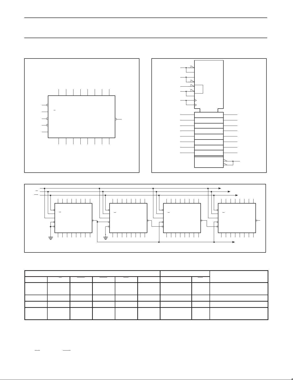
Figure 1. Synchronous Multistage Counting Scheme


MODE SELECT FUNCTION TABLE


INPUTS


OUTPUTS


OPERATING MODE


CP


U/D


CEP


CET


PE


Pn


Qn


TC


X


X


X


l


l


L


(a)


Parallel load


X


X


X


l


h


H


(a)


h


l


l


h


X


Count Up


(a)


Count Up


l


l


l


h


X


Count Down


(a)


Count Down


X


h


l


h


X


qn


(a)


Hold (do nothing)


X


X


h


h


X


qn


H


H

=


High voltage level


h

=


High voltage level one setup prior to the Low-to-High clock transition


L

=


Low voltage level


l

=


Low voltage level one setup time prior to the Low-to-High clock transition


q

=


Lower case letters indicate the state of the referenced output prior to the Low-to-High clock transition


X

=


Don't care


=


Low-to-High clock transition


(a) = TC is Low when CET is Low and the counter is at Terminal Count. Terminal Count Up is with all Qn outputs High and Terminal Count Down is with all Qn outputs Low.

1996 Jan 05

3

Philips N74F269D, N74F269N, N74F269DB Datasheet

Philips Semiconductors

Product specification


8±bit bidirectional binary counter

74F269


LOGIC DIAGRAM

P0

23

DETAIL A

2

Q0


P1

22

DETAIL A

3

Q1


P2

21

DETAIL A

4

Q2


P3

20

DETAIL A

5

Q3


P4

18

DETAIL A

6

Q4


P5

17

DETAIL A

8

Q5


P6

16

DETAIL A

9

Q6


P7

15

DETAIL A

10 Q7


PE

24


CP

11


U/D

1


CEP

12


CET

13


TOGGLE

14

TC


DETAIL A


Pn


D

Q


CP

Q


PE


CP


VCC=Pin 19


GND=Pin 7


SF00837


1996 Jan 05


4


Philips Semiconductors

Product specification


8±bit bidirectional binary counter

74F269


ABSOLUTE MAXIMUM RATINGS

(Operation beyond the limits set forth in this table may impair the useful life of the device. Unless otherwise noted these limits are over the operating free-air temperature range.)

SYMBOL

PARAMETER

RATING

UNIT


VCC

Supply voltage

±0.5 to +7.0

V

VIN

Input voltage

±0.5 to +7.0

V

IIN

Input current

±30 to +5

mA

VOUT

Voltage applied to output in High output state

±0.5 to VCC

V

IOUT

Current applied to output in Low output state

40

mA

Tamb

Operating free-air temperature range

0 to +70

°C

Tstg

Storage temperature

±65 to +150

°C

RECOMMENDED OPERATING CONDITIONS

SYMBOL

PARAMETER


LIMITS


UNIT


MIN

NOM

MAX


VCC

Supply voltage

4.5

5.0

5.5

V

VIH

High-level input voltage

2.0


V

VIL

Low-level input voltage


0.8

V

IIK

Input clamp current


±18

mA

IOH

High-level output current


±1

mA

IOL

Low-level output current


20

mA

Tamb

Operating free-air temperature range

0


70

°C

DC ELECTRICAL CHARACTERISTICS

(Over recommended operating free-air temperature range unless otherwise noted.)


LIMITS


SYMBOL

PARAMETER


TEST CONDITIONSNO TAG


UNIT


MIN

TYP

MAX


NO TAG


VOH

High-level output voltage

VCC = MIN, VIL = MAX


±10%VCC

2.5


V

VIH = MIN, IOH = MAX


±5%VCC

2.7

3.4


VOL

Low-level output voltage

VCC = MIN, VIL = MAX


±10%VCC


0.30

0.50

V

VIH = MIN, IOL = MAX


±5%VCC


0.30

0.50


VIK

Input clamp voltage

VCC = MIN, II = IIK


±0.73

±1.2

V

II

Input current at maximum input voltage

VCC = MAX, VI = 7.0V


100

mA

IIH

High-level input current

VCC = MAX, VI = 2.7V


20

mA

IIL

Low-level input current

VCC = MAX, VI = 0.5V


±0.6

mA

I

Short-circuit output currentNO TAG

V = MAX


±60


±150

mA

OS


CC


ICCH


PE=CET=CEP=U/D=GND,


93

120

mA


VCC =


Pn=4.5V, CP=↑


ICC

Supply current (total)


MAX


ICCL


PE=CET=CEP=U/D=GND,


98

125

mA


Pn=GND, CP=↑


NOTES:

1.For conditions shown as MIN or MAX, use the appropriate value specified under recommended operating conditions for the applicable type.

2.All typical values are at VCC = 5V, Tamb = 25°C.

3.Not more than one output should be shorted at a time. For testing IOS, the use of high-speed test apparatus and/or sample-and-hold techniques are preferable in order to minimize internal heating and more accurately reflect operational values. Otherwise, prolonged shorting of a High output may raise the chip temperature well above normal and thereby cause invalid readings in other parameter tests. In any sequence of parameter tests, IOS tests should be performed last.

1996 Jan 05

5

Loading...
+ 9 hidden pages