

Philips N74F256D Datasheet
INTEGRATED CIRCUITS
74F256
Dual addressable latch
Product specification
IC15 Data Handbook
1988 Nov 29
Philips Semiconductors Product specification
74F256Dual addressable latch
FEA TURES
•Combines dual demultiplexer and 8-bit latch
•Serial-to-parallel capability
•Output from each storage bit available
•Random (addressable) data entry
•Easily expandable
•Common reset input
•Useful as dual 1-of-4 active High decoder
DESCRIPTION
The 74F256 dual addressable latch has four distinct modes of
operation which are selectable by controlling the Master Reset (MR
and Enable (E
mode, data at the Data inputs is written into the addressed latches.
The addressed latches will follow the Data input with all
unaddressed latches remaining in their previous states. In the
memory mode, all latches remain in their previous states and are
unaffected by the Data or Address inputs. To eliminate the possibility
of entering erroneous data in the latches, the enable should be held
High (inactive) while the address lines are changing. In the dual
1-of-4 decoding or demultiplexing mode (MR
outputs will follow the level of the Data inputs, with all other outputs
Low. In the Master Reset mode, all outputs are Low and unaffected
by the Address and Data inputs.
) inputs (see Function Table). In the addressable latch
=E=Low), addressed
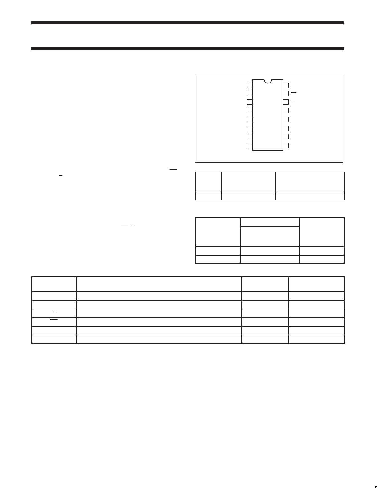
PIN CONFIGURATION
)
TYPE TYPICAL
PROPAGATION
74F256 7.0ns 28mA
ORDERING INFORMATION
DESCRIPTION COMMERCIAL RANGE
16-pin plastic DIP N74F256N SOT38-4
16-pin plastic SO N74F256D SOT109-1
1
A0
2
A1
3
Da
4
Q0a
5
Q1a
6
Q2a
Q3a
GND
DELAY
ORDER CODE
VCC = 5V ±10%,
T
amb
16
15
14
13
12
11
107
98
SF00805
CURRENT (TOTAL)
= 0°C to +70°C
V
CC
MR
E
Db
Q3b
Q2b
Q1b
Q0b
TYPICAL SUPPL Y
PKG DWG #
INPUT AND OUTPUT LOADING AND FAN OUT TABLE
PINS DESCRIPTION 74F (U.L.)
HIGH/LOW
Da, Db Port A, port B inputs 1.0/1.0 20µA/0.6mA
A0, A1 Address inputs 1.0/1.0 20µA/0.6mA
E Enable (active Low) 1.0/1.0 20µA/0.6mA
MR Master Reset inputs (active Low) 1.0/1.0 20µA/0.6mA
Q0a – Q3a Port A outputs 50/33 1.0mA/20mA
Q0b – Q3b Port B outputs 50/33 1.0mA/20mA
NOTE:
One (1.0) FAST unit load is defined as: 20µA in the High state and 0.6mA in the Low state.
LOAD VALUE
HIGH/LOW
1988 Nov 29 853–0359 95207
2
Philips Semiconductors Product specification
OPERATING MODE
Addressable Latch
74F256Dual addressable latch
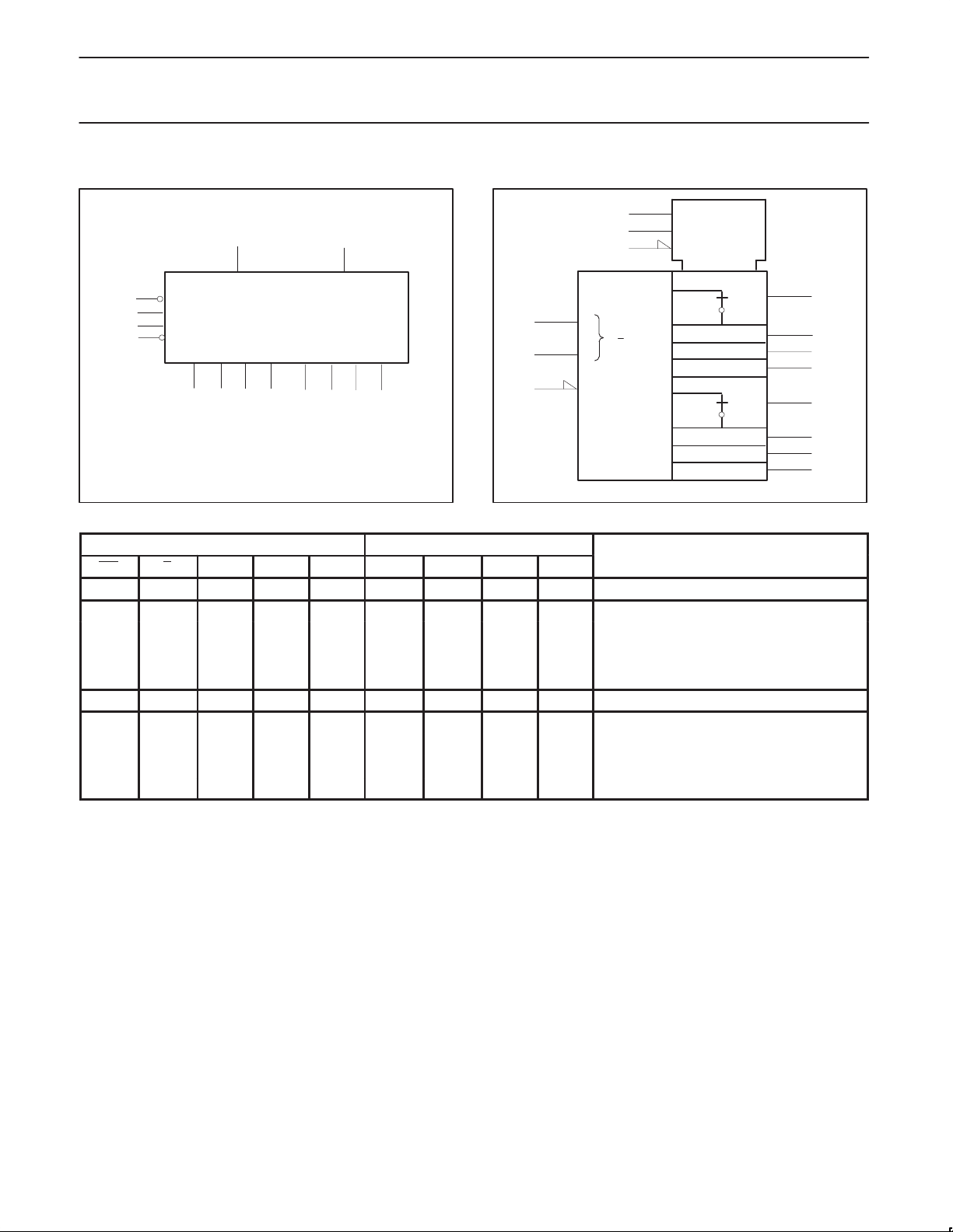
LOGIC SYMBOL
E
14
A0
1
A1
2
MR
15
VCC = Pin 16
GND = Pin 8
Q0a Q1a Q2a Q3a Q0b Q1b Q2b Q3b
313
Da Db
4567 9101112
SF00806
IEC/IEEE SYMBOL
1
2
14
0
G
1
3
13
15
0
3
Z5
Z6
G4
5, 7D
1
0
1
2
3
6, 8D
1
0
1
2
3
C7
4R
C8
4R
4
5
6
7
9
10
11
12
SF00807
FUNCTION TABLE
INPUTS OUTPUTS
MR E D A0 A1 Q0 Q1 Q2 Q3
L H X X X L L L L Master Reset
L L d L L Q=d L L L
L L d H L L Q=d L L
L L d L H L L Q=d L
L L d H H L L L Q=d
H H X X X q0 q1 q2 q3 Store (do nothing)
H L d L L Q=d q1 q2 q3
H L d H L q0 Q=d q2 q3
H L d L H q0 q1 Q=d q3
H L d H H q0 q1 q2 Q=d
H = High voltage level
L = Low voltage level
X = Don’t care
d = High or Low data one setup time prior to the Low-to-High Enable transition
q = Lower case letters indicate the state of the referenced output established during the last cycle in which it was addressed or cleared.
Demultiplex (active-High decoder when D=H)
1988 Nov 29
3
Philips Semiconductors Product specification
74F256Dual addressable latch
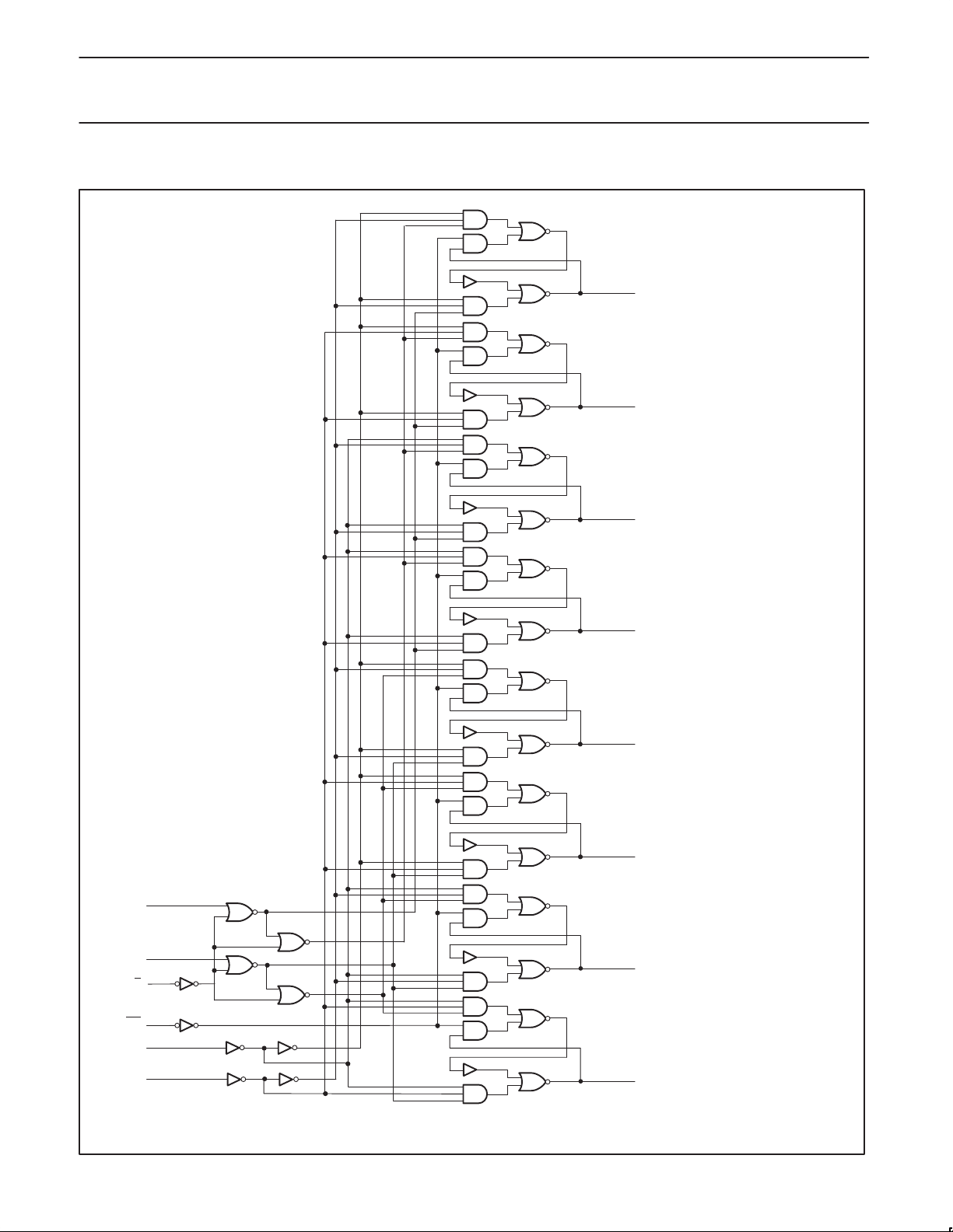
LOGIC DIAGRAM
12
Q3b
11
Q2b
10
Q1b
9
Q0b
7
Q3a
6
Q2a
13
Db
3
Da
14
E
5
Q1a
MR
A1
A0
VCC = Pin 16
GND = Pin 8
1988 Nov 29
15
2
1
4
SF00808
Q0a
4
 Loading...