

Philips N74ALS04BD, N74ALS04BDB, N74ALS04BN Datasheet
74ALS04B
Hex inverter
Product specification 1991 Feb 08
INTEGRATED CIRCUITS
IC05 Data Handbook
Philips Semiconductors Product specification
74ALS04BHex inverter
2
1991 Feb 08 853–0856 01670
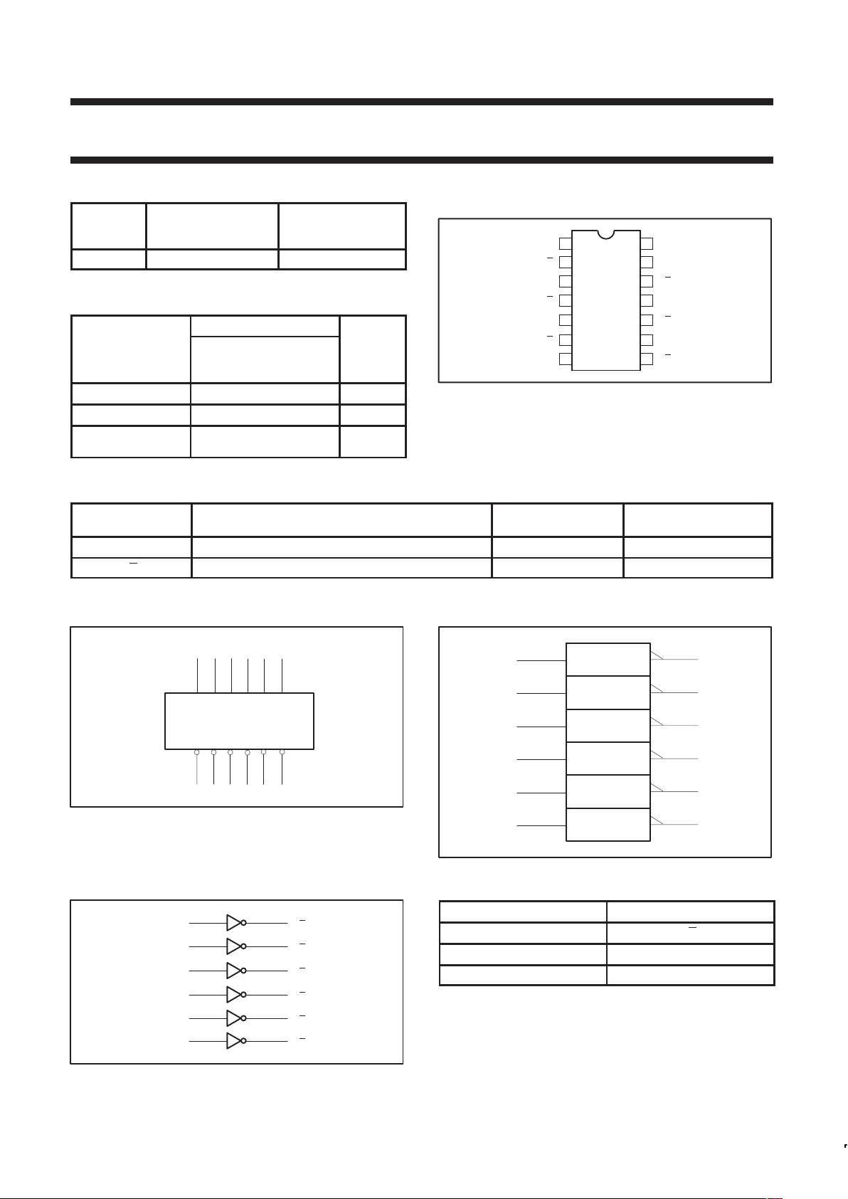
TYPE
TYPICAL
PROPAGATION DELAY
TYPICAL
SUPPLY CURRENT
(TOTAL)
74ALS04B 3.5ns 2.0mA
ORDERING INFORMATION
ORDER CODE
DESCRIPTION COMMERCIAL RANGE
V
CC
= 5V ±10%,
T
amb
= 0°C to +70°C
DRAWING
NUMBER
14-pin plastic DIP 74ALS04BN SOT27-1
14-pin plastic SO 74ALS04BD SOT108-1
14-pin plastic SSOP
Type II
74ALS04BDB SOT337-1
PIN CONFIGURATION
14
13
12
11
10
9
87
6
5
4
3
2
1
GND
V
CC
5Y
4A
4Y
5A
6A
6Y
1A
1Y
3Y
2A
2Y
3A
SF00011
INPUT AND OUTPUT LOADING AND FAN-OUT TABLE
PINS DESCRIPTION
74ALS (U.L.)
HIGH/LOW
LOAD VALUE
HIGH/LOW
nA Data input 1.0/1.0 20µA/0.1mA
nY Data output 20/80 0.4mA/8mA
NOTE: One (1.0) ALS unit load is defined as: 20µA in the High state and 0.1mA in the Low state.
LOGIC SYMBOL
46810
13591113
VCC = Pin 14
GND = Pin 7
SF00013
1A 2A 3A 4A 5A 6A
2
1A 2A 3A 4A 5A 6A
12
IEC/IEEE SYMBOL
13
1
SF00014
12
11
10
9
8
5
6
3
4
1
2
LOGIC DIAGRAM
VCC = Pin 14
GND = Pin 7
SF00012
2
4
6
8
10
12
1Y
2Y
3Y
4Y
5Y
6Y
1
3
5
9
11
13
1A
2A
3A
4A
5A
6A
FUNCTION TABLE
INPUT OUTPUT
nA nY
L H
H L
H = High voltage level
L = Low voltage level
Philips Semiconductors Product specification
74ALS04BHex inverter
1991 Feb 08
3
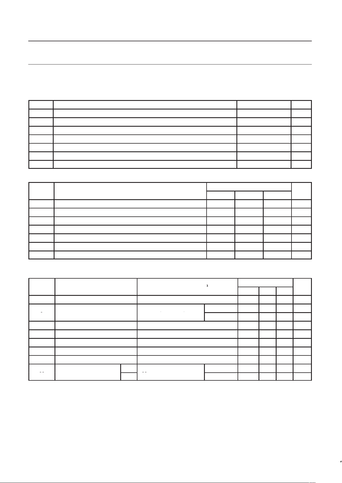
ABSOLUTE MAXIMUM RATINGS
(Operation beyond the limit set forth in this table may impair the useful life of the device.
Unless otherwise noted these limits are over the operating free-air temperature range.)
SYMBOL
PARAMETER RATING UNIT
V
CC
Supply voltage –0.5 to +7.0 V
V
IN
Input voltage –0.5 to +7.0 V
I
IN
Input current –30 to +5 mA
V
OUT
Voltage applied to output in High output state –0.5 to V
CC
V
I
OUT
Current applied to output in Low output state 16 mA
T
amb
Operating free-air temperature range 0 to +70 °C
T
stg
Storage temperature range –65 to +150 °C
RECOMMENDED OPERATING CONDITIONS
LIMITS
SYMBOL
PARAMETER
MIN NOM MAX
UNIT
V
CC
Supply voltage 4.5 5.0 5.5 V
V
IH
High-level input voltage 2.0 V
V
IL
Low-level input voltage 0.8 V
I
Ik
Input clamp current –18 mA
I
OH
High-level output current –0.4 mA
I
OL
Low-level output current 8 mA
T
amb
Operating free-air temperature range 0 +70 °C
DC ELECTRICAL CHARACTERISTICS
(Over recommended operating free-air temperature range unless otherwise noted.)
LIMITS
SYMBOL
PARAMETER
TEST CONDITIONS
1
MIN TYP2MAX
UNIT
V
OH
High-level output voltage VCC±10%, VIL = MAX, VIH = MIN, IOH = –0.4mA V
CC
– 2 V
p
VCC = MIN, VIL = MAX,
I
OL
= 4mA 0.25 0.40 V
VOLLow-level output voltage
CC
,
IL
,
VIH = MIN
I
OL
= 8mA 0.35 0.50 V
V
IK
Input clamp voltage VCC = MIN, II = I
IK
-0.73 -1.5 V
I
I
Input current at maximum input voltage VCC = MAX, VI = 7.0V 0.1 mA
I
IH
High-level input current VCC = MAX, VI = 2.7V 20 µA
I
IL
Low-level input current VCC = MAX, VI = 0.5V -0.1 mA
I
O
Output current
3
VCC = MAX, VO = 2.25V -30 -112 mA
pp
I
CCH
VI = GND 0.75 1.1 mA
ICCSupply current (total)
I
CCL
V
CC
=
MAX
VI = 4.5V 3.2 4.2 mA
NOTES:
1. For conditions shown as MIN or MAX, use the appropriate value specified under recommended operating conditions for the applicable type.
2. All typical values are at V
CC
= 5V, T
amb
= 25°C.
3. The output conditions have been chosen to produce a current that closely approximate one half of the true short-circuit output current, I
OS
.
 Loading...