

Philips MX3950D, MX3960D, MX3910D, MX3900D Service Manual

Service Manual
Service
Service
DVD Receiver
MX3900D/37 & MX3910D/17
Service
Service
Service
MX3950D/
37 & MX3960D/17
©
Copyright 2003 Philips Consumer Electronics B.V. Eindhoven, The Netherlands
All rights reserved. No part of this publication may be reproduced, stored in a retrieval system or
transmitted, in any form or by any means, electronic, mechanical, photocopying, or otherwise
without the prior permission of Philips.
Published by KC 0311 Service Audio Printed in The Netherlands Subject to modification
Version 1.1
TABLE OF CONTENTS
Page
Location of pc boards & Version variations ................1-2
Technical Specifications ............................................. 1-3
Measurement setup ....................................................1-4
Service Aids, Safety Instruction, etc. .........................1-5
Disassembly Instructions & Service positions ........... 2-1
Service Test Programs ...............................................3-1
Region codes setting, software upgrades, etc ...........3-3
Set Block diagram.......................................................... 4
Set Wiring diagram ........................................................ 5
Front Board .................................................................... 6
ECO6 Tuner Board: System Non-Cenelec ............ 7A
Power Module PWR207 ................................................8
AV Board........................................................................ 9
5DTC Module............................................................... 10
CD222 FE (Front End) Board ......................................11
CD222 BE (Back End) Board ...................................... 12
Set Mechanical Exploded view & parts list ................. 13
Revision List ................................................................ 14
CLASS 1
LASER PRODUCT
GB
3139 785 30201
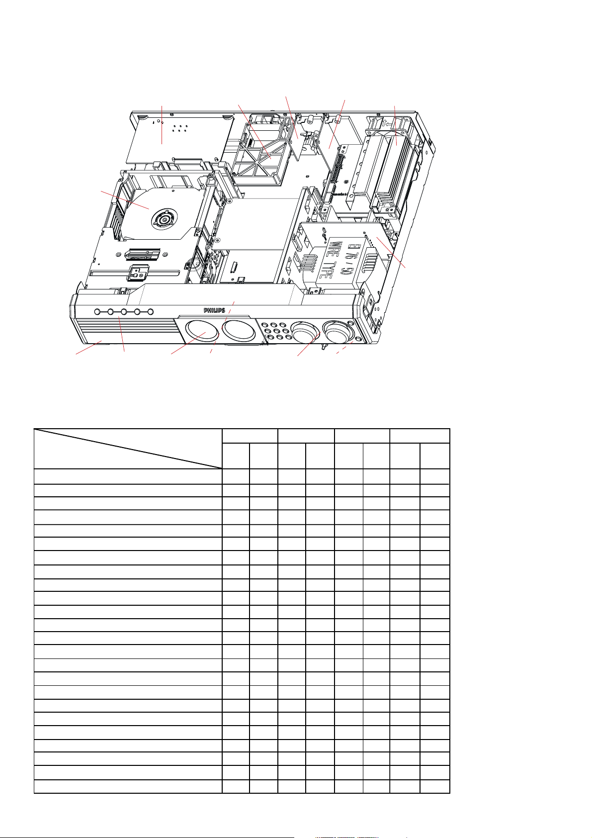
LOCATION OF PC BOARDS
1-2
FRONT
STANDBY
PAR T
5DTC-DVD
LOADER
MECHANISM
+
CONTROL
BOARD
FRONT
DTC KEY
PAR T
MAINS & ECO
STBY BOARD
FRONT
DISPLAY
PAR T
ECO6 TUNER
BOARD
PCMCIA BOARD
(just in front of the
CD222 FE board)
CD222 FE
BOARD
CD222 BE
BOARD
SPK II BOARD
AV BOARD
FRONT
CONTROL
PAR T
SPK I BOARD
FRONT
HP & MIC
PAR T
AMPLIFER BOARD
100W = 2PCS
75W = 1PC
SUPPLY
BOARD
VERSION VARIATIONS:
Type /Versions: MX3900D MX3910D MX3950D MX3960D
Features &
/37 /37 /37 /17
Board in used:
Karaoke - - - -
News - - - RDS - - - Pro-Scan x x x x
PCMCIA - - - Standby - Clock Display x x x x
ECO Standby - No Display x x x x
Voltage Selector - - - -
Digital In / Out x x x x
Aux Input x x x x
TV Input x x x x
Line Output x x x x
SCART output - - - Pr, Pb & Y Outputs x x x x
CVBS Output x x x x
S-Video Output x x x x
Headphone Socket x x x x
Tuner board - ECO6 System non-Cenelec x x x x
Tuner board - ECO6 System Cenelec - - - Amplifier board - 1pc (75W 6-Channel) x x x x
Amplifier board - 1pc (75W 7-Channel) - - - Amplifier board - 2pc (100W 6-Channel) - - - -

SPECIFICATIONS
1-3
GENERAL:
Mains voltage : 120V
Mains frequency : 60Hz
Power consumption : < 0,5W at ECO Standby
< 20W Standby (clock display)
Clock accuracy : < 4 seconds per day
Dimension centre unit : 435 x 100 x 360mm
TUNER:
FM
Tuning range : 87.5-108MHz
Grid : 50kHz
IF frequency : 10.7MHz ± 25kHz
Aerial input : 75Ω coaxial
Sensitivity at 26dB S/N : < 7µV
Selectivity at 600kHz bandwidth : > 25dB
Image rejection : > 25dB
Distortion at RF=1mV, dev. 75kHz : < 3%
-3dB Limiting point : < 8µV
Crosstalk at RF=1mV, dev. 40kHz : > 18dB
MW
Tuning range : 530-1700kHz
Grid : 10kHz
IF frequency : 450kHz ± 1kHz
Aerial input : Frame aerial
Sensitivity at 26dB S/N : < 4.0mV/M
Selectivity at 18kHz bandwidth : > 18dB
IF rejection : > 45dB
Image rejection : > 28dB
Distortion at RF=50mV, m=80% : < 5%
COMPACT DISC/VCD/DVD:
Video Decoding : MPEG-2
Video DAC : 10 Bits
Signal System : PAL / NTSC
Video Format : 4:3 / 16:9
MP3-CD bit rate
MP3-CD sampling frequencies
CBVS out
4)
5)
CVBS level : 1.0 ± 0.1V
: 32-256 kbs,variable bitrates
4)
: 32kHz, 44.1kHz, 48kHz
p-p
Luminance S/N ratio : > 45dB (unweighted)
YUV out
5)
Amplitude : 714mV ± 7mV
S/N ratio : > 50dB (unweighted)
S-Video out
5)
Y level : 1.0 ± 0.1V
p-p
Y S/N ratio : > 48dB (unweighted)
C level (burst) : 286mV
+1/-4 dB
p-p
Digital Out : Coaxial acc IEC61937 / IEC60958
Digital In : Coaxial acc IEC60958
1)
with only channel(s) under meausrement loaded, all other
channels are unloaded.
2)
Frequency response in each setting is software controlled.
3)
measured with 55Hz at vol. maximum.
4)
Recording format: ISO9660, UDF format is not supported.
5)
Output terminals terminated with 75Ω
AMPLIFIER:
1)
Output power
at 4Ω, 1 kHz, 10% THD
L/R : 2 x 75W RMS
2 x 60W FTC
Center : 72W
Surround L/R : 72W RMS/channel
Sub-woofer : 72W
Frequency response ±3dB : 20Hz-20kHz
Hum (minimum volume) : 200nW
Residue noise (min, volume) : 40nW
Digital Sound Control : Stereo, 3D Sound, Multi modes
Bass & Treble : -3dB to +3dB
Input sensitivity
TV-in : 350mV ± 3dB
Aux-in : 880mV ± 2dB
Output sensitivity
Line out : 600mV ± 2dB at 47kΩ
Subwoofer out 3): 1.85V ± 2dB at 47kΩ
Headphone (vol. max.) : 660mV ± 2dB at 32Ω
Center out (vol. max.) : 500mV ± 2dB at 47kΩ
2)
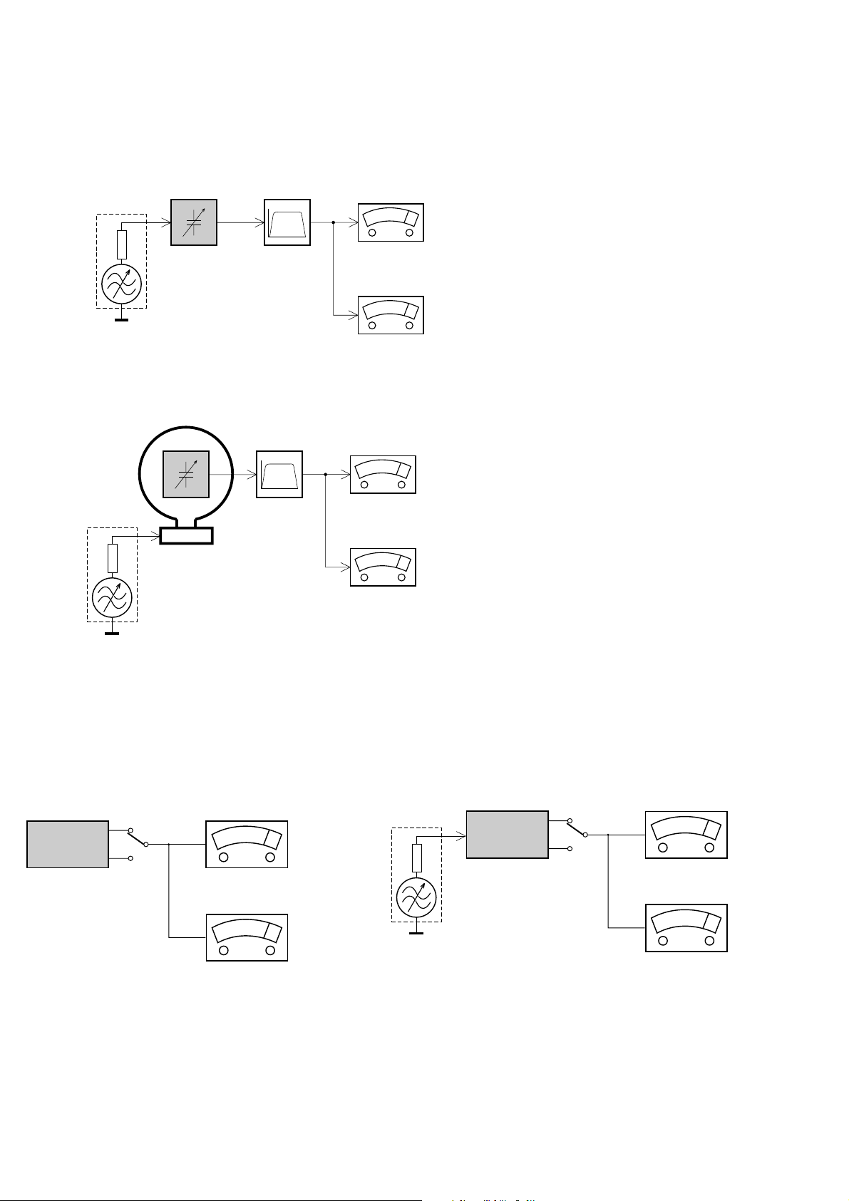
MEASUREMENT SETUP
Tuner FM
1-4
Bandpass
LF Voltmeter
e.g. PM2534
RF Generator
e.g. PM5326
DUT
250Hz-15kHz
e.g. 7122 707 48001
Ri=50Ω
S/N and distortion meter
e.g. Sound Technology ST1700B
Use a bandpass filter to eliminate hum (50Hz, 100Hz) and disturbance from the pilottone (19kHz, 38kHz).
Tuner AM (MW,LW)
RF Generator
e.g. PM5326
Ri=50Ω
DUT
Frame aerial
e.g. 7122 707 89001
Bandpass
250Hz-15kHz
e.g. 7122 707 48001
LF Voltmeter
e.g. PM2534
S/N and distortion meter
e.g. Sound Technology ST1700B
To avoid atmospheric interference all AM-measurements have to be carried out in a Faraday´s cage.
Use a bandpass filter (or at least a high pass filter with 250Hz) to eliminate hum (50Hz, 100Hz).
CD
Use Audio Signal Disc
(replaces test disc 3)
DUT
L
R
SBC429 4822 397 30184
S/N and distortion meter
e.g. Sound Technology ST1700B
LEVEL METER
e.g. Sennheiser UPM550
with FF-filter
Recorder
Use Universal Test Cassette CrO2 SBC419 4822 397 30069
or Universal Test Cassette Fe SBC420 4822 397 30071
LF Generator
e.g. PM5110
DUT
L
R
S/N and distortion meter
e.g. Sound Technology ST1700B
LEVEL METER
e.g. Sennheiser UPM550
with FF-filter
SERVICE AIDS
1-5
Service Tools:
Universal Torx driver holder .................................. 4822 395 91019
Torx bit T10 150mm ............................................. 4822 395 50456
Torx driver set T6 - T20 ......................................... 4822 395 50145
Torx driver T10 extended ...................................... 4822 395 50423
Allen key set (1.5, 2, 2.5, 3, 4, 5, 6, 8mm) ............ 5322 395 10754
Compact Disc:
SBC426/426A Test disc 5 + 5A ............................ 4822 397 30096
SBC442 Audio Burn-in Test disc 1kHz ................. 4822 397 30155
SBC429 Audio Signals disc .................................. 4822 397 30184
SBC444/444A ........................................................ 4822 397 30245
CD-RW Printed Audio Test Disc ........................... 7104 099 96611
Dolby Pro-logic Test Disc ...................................... 4822 395 10216
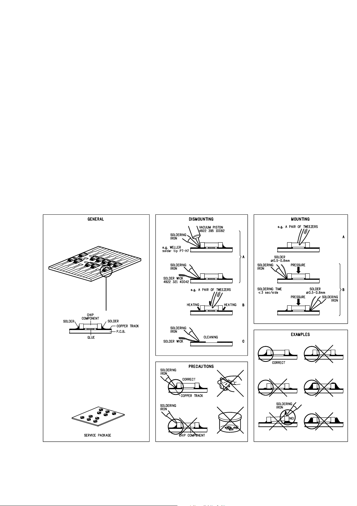
HANDLING CHIP COMPONENTS
ESD Equipment:
Anti-static table mat - large 1200x650x1.25mm ... 4822 466 10953
Anti-static table mat - small 600x650x1.25mm ..... 4822 466 10958
Anti-static wristband .............................................. 4822 395 10223
Connector box (1MΩ) ............................................ 4822 320 11307
Extension cable
(to connect wristband to conn. box) .................. 4822 320 11305
Connecting cable
(to connect table mat to conn. box) .................. 4822 320 11306
Earth cable (to connect product to mat or box) .... 4822 320 11308
Complete kit ESD3
(combining all above products) ......................... 4822 320 10671
Wristband tester .................................................... 4822 344 13999
WARNING
GB
All ICs and many other semi-conductors are
susceptible to electrostatic discharges (ESD).
Careless handling during repair can reduce life
drastically.
When repairing, make sure that you are
connected with the same potential as the mass
of the set via a wrist wrap with resistance.
Keep components and tools also at this
potential.
F
ATTENTION
Tous les IC et beaucoup d’autres
semi-conducteurs sont sensibles aux
décharges statiques (ESD).
Leur longévité pourrait être considérablement
écourtée par le fait qu’aucune précaution n’est
prise à leur manipulation.
Lors de réparations, s’assurer de bien être relié
au même potentiel que la masse de l’appareil et
enfiler le bracelet serti d’une résistance de
sécurité.
Veiller à ce que les composants ainsi que les
outils que l’on utilise soient également à ce
potentiel.
1-6
ESD
D
WARNUNG
Alle ICs und viele andere Halbleiter sind
empfindlich gegenüber elektrostatischen
Entladungen (ESD).
Unsorgfältige Behandlung im Reparaturfall kan
die Lebensdauer drastisch reduzieren.
Veranlassen Sie, dass Sie im Reparaturfall über
ein Pulsarmband mit Widerstand verbunden
sind mit dem gleichen Potential wie die Masse
des Gerätes.
Bauteile und Hilfsmittel auch auf dieses gleiche
Potential halten.
WAARSCHUWING
NL
Alle IC’s en vele andere halfgeleiders zijn
gevoelig voor electrostatische ontladingen
(ESD).
Onzorgvuldig behandelen tijdens reparatie kan
de levensduur drastisch doen verminderen.
Zorg ervoor dat u tijdens reparatie via een
polsband met weerstand verbonden bent met
hetzelfde potentiaal als de massa van het
apparaat.
Houd componenten en hulpmiddelen ook op
ditzelfde potentiaal.
I
AVVERTIMENTO
Tutti IC e parecchi semi-conduttori sono
sensibili alle scariche statiche (ESD).
La loro longevità potrebbe essere fortemente
ridatta in caso di non osservazione della più
grande cauzione alla loro manipolazione.
Durante le riparazioni occorre quindi essere
collegato allo stesso potenziale che quello della
massa dell’apparecchio tramite un braccialetto
a resistenza.
Assicurarsi che i componenti e anche gli utensili
con quali si lavora siano anche a questo
potenziale.
GB
Safety regulations require that the set be restored to its original
condition and that parts which are identical with those specified,
be used.
NL
Veiligheidsbepalingen vereisen, dat het apparaat bij reparatie in
zijn oorspronkelijke toestand wordt teruggebracht en dat onderdelen,
identiek aan de gespecificeerde, worden toegepast.
F
Les normes de sécurité exigent que l’appareil soit remis à l’état
d’origine et que soient utiliséés les piéces de rechange identiques
à celles spécifiées.
D
Bei jeder Reparatur sind die geltenden Sicherheitsvorschriften zu
beachten. Der Original zustand des Geräts darf nicht verändert werden;
für Reparaturen sind Original-Ersatzteile zu verwenden.
“Pour votre sécurité, ces documents
doivent être utilisés par des spécialistes agréés, seuls habilités à réparer
votre appareil en panne”.
CLASS 1
LASER PRODUCT
GB
Invisible laser radiation when open.
Avoid direct exposure to beam.
Osynlig laserstrålning när apparaten är öppnad och spärren
är urkopplad. Betrakta ej strålen.
Warning !
S
Varning !
3122 110 03420
I
Le norme di sicurezza esigono che l’apparecchio venga rimesso
nelle condizioni originali e che siano utilizzati i pezzi di ricambio
identici a quelli specificati.
"After servicing and before returning set to customer perform a
leakage current measurement test from all exposed metal parts to
earth ground to assure no shock hazard exist. The leakage current
must not exceed 0.5mA."
Varoitus !
SF
Avatussa laitteessa ja suojalukituksen ohitettaessa olet alttiina
näkymättömälle laserisäteilylle. Älä katso säteeseen!
DK Advarse !
Usynlig laserstråling ved åbning når sikkerhedsafbrydere er
ude af funktion. Undgå udsaettelse for stråling.
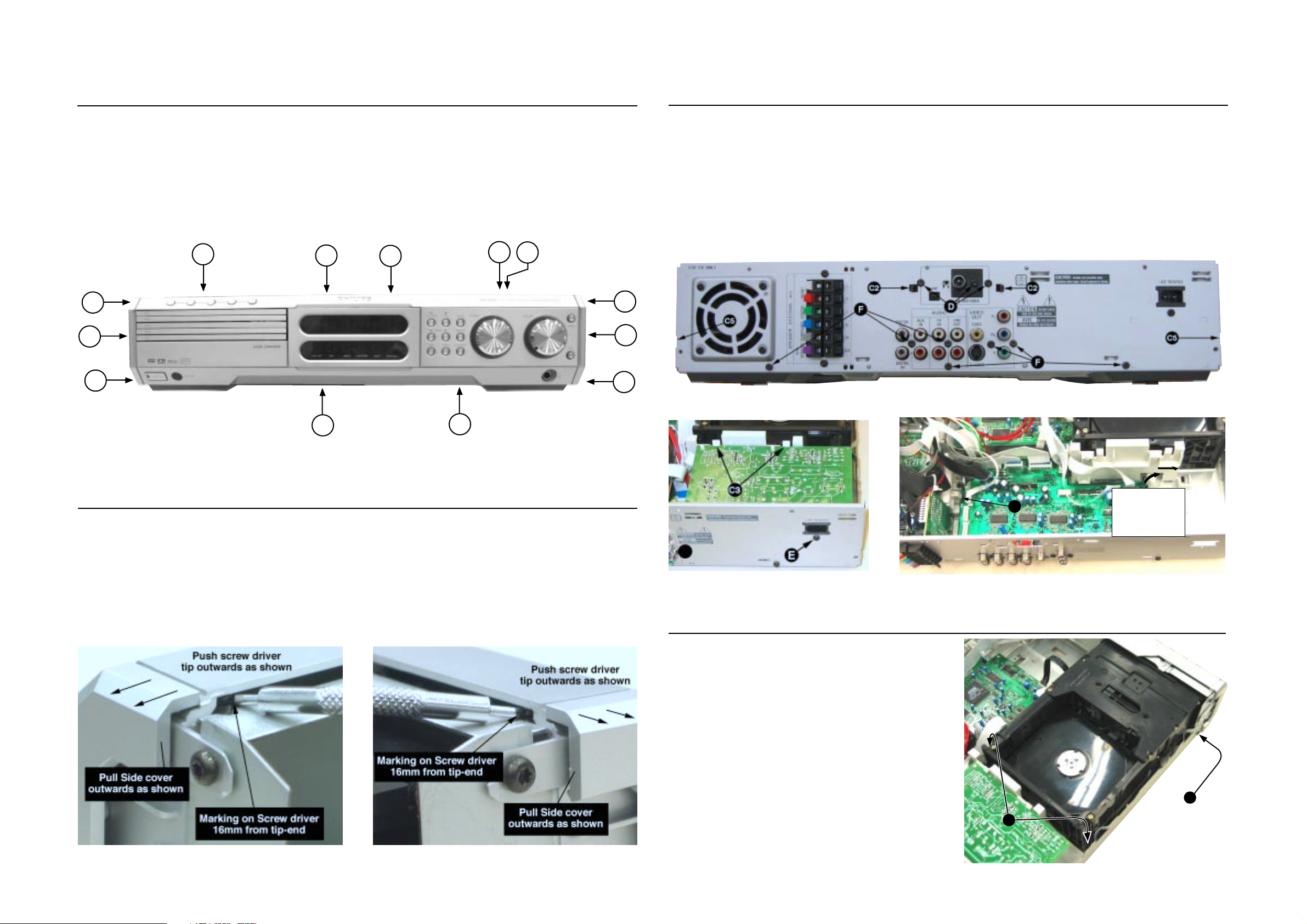
DISMANTLING INSTRUCTIONS
C4
1
2
Turn up the lever,
slide the bracket
as shown and lift
out of the bottom
chassis.
2-1 2-1
Dismantling of the Front Panel assembly
1) Loosen the 9 screws to dismantle the Top Cover (pos
252)
- 2 screws on each side
- 5 screws on the Rear Panel (pos 251).
C1
C1
A
C1
A
2) Loosen 5 screws A and 8 catches C1 to slide the Front
Panel assembly (pos 101, 102, 103, etc) as per figure 1.
Note: To remove the Source / Volume control pc
board (pos 1105B) 2 nuts hidden below the
control knob assembly (pos 133, 134 and 135)
must first be removed.
C1
C1
A
A
C1
A
Dismantling the Tuner, Mains and AV boards
1) Loosen 3 screws D and 2 catches C2 on the Rear panel
(pos 251) to remove the Tuner board assemby (pos 1101)
as pe figure 3.
2) Loosen 1 screws E and 2 catches C3 to unslot the Mains
board (pos 1102-A) out of the Rear panel as per figure 4.
3) Loosen bracket (pos 254) by turning a catch, sliding
towards the outside and lifting it upwards as per figure 5.
4) Loosen 7 screws F and 2 C5 to separate Rear Plate
assembly (pos 251 + 227) from the Bottom plate as per
figure 3.
5) Uncatch C4 to remove the AV board (pos 1104) from the
Bottom & Rear Plate assembly (pos 251 + 227) as per
figure 5.
Figure 3
C1
Hints for re-assembly of Top Cover
Due to appearance design the Top cover (pos 252) is
sandwiched between the Front panel (pos 101) and the 2
side covers (pos 102 & 103), this make it necessary to
remove the 2 side covers before re-assembly of Top cover.
Figure 1
C1
1) To remove the side cover use a small screw driver with
marking 16mm from the tip end.
2) Insert the screw driver into slot (as shown in figure 2) and
push the tip outwards to release the side cover catch.
The side cover can be pull outwards as soon as the top
catch is released.
Figure 4
Dismantling the 5DTC Module
1) Loosen 1 screws E and 2 catches C3 to remove the
Mains board as per figure 4.
2) Loosen bracket (pos 254) by turning a catch, sliding
towards the outside and lifting it upwards as per figure 5.
3) Loosen 3 screws G, lift up the 5DTC Module's (pos 1103-
A) rear and pull the module out towards the rear as per
figure 6.
Figure 5
G
G
Figure 2
Figure 6
2-2
2-2
Service positions
Dismantling the Mono FE and BE boards
1) Loosen 2 screws and 2 catches to remove the Mono BE
board (pos 1103-B).
2) Loosen 2 screws and 2 catches to remove the Mono FE
board (pos 1103-C).
Dismantling the Supply & Power Amplifier boards
1) Loosen 2 screws B mounting the Supply board's (pos
1102-B) heatsink to the Bottom Plate (pos 227) as per
figure 7.
Note: During re-assembly care must be taken to
ensure the Mains Transformer wires to the
Supply board is routed properly below the
board.
Service position A (Top cover removed)
2) Loosen 4 screws C to dismantle the Power Amplifier
board (pos 1102-D) from the Bottom Plate as per figure
7.
Figure 7
Service position B (Front Panel loosen)
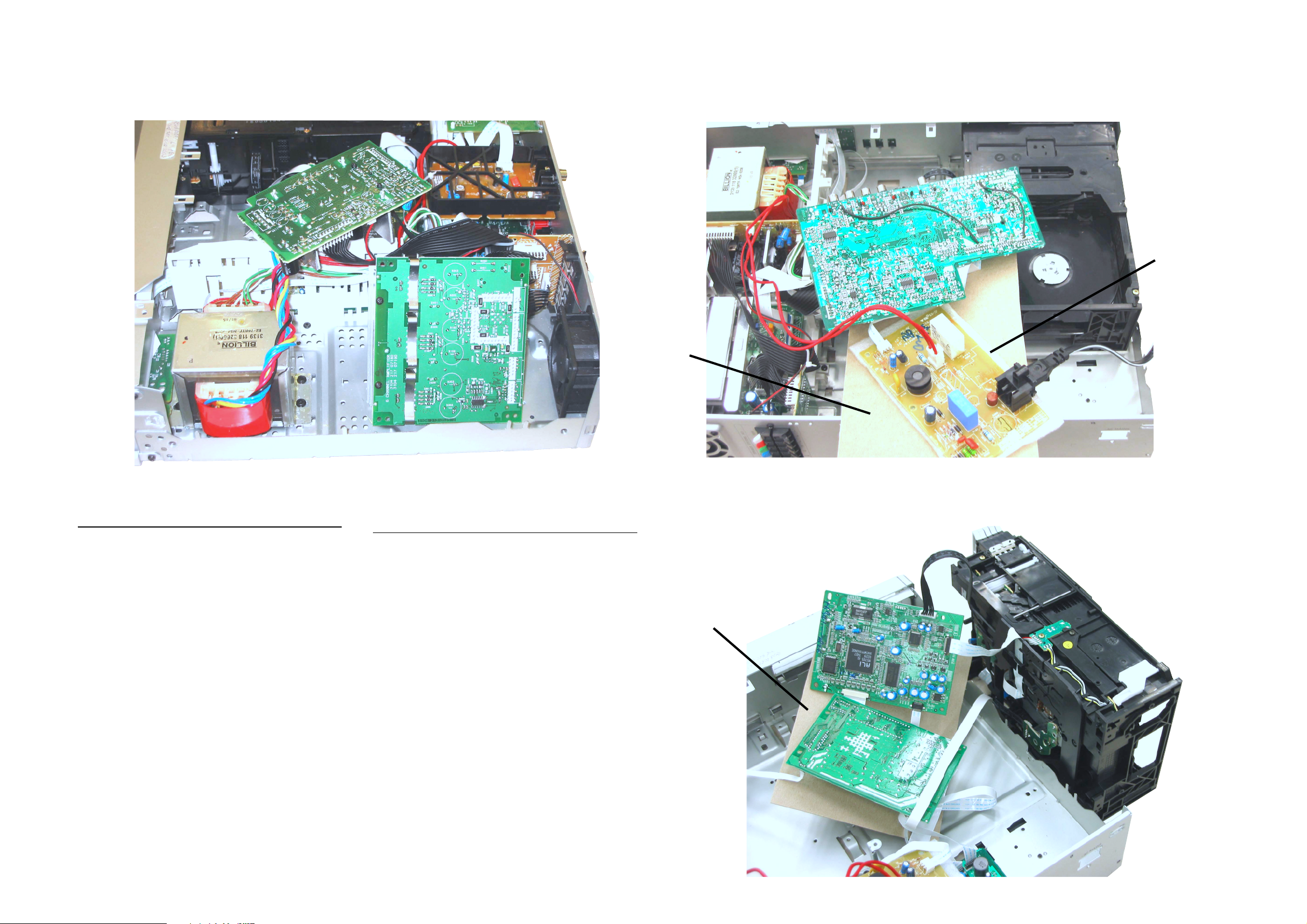
Service positions
2-3 2-3
Service position C (Supply and Amplifier boards loosen)
Service position D (Mains & AV boards loosen)
Mains Board
with non-
conductive
insulation
attached to the
copper pattern
Thick paper
Caution:
1) In some of the service positions the Mains supply is
exposed, therefore service technicians have to exercise
care to prevent electric shock.
2) The copper pattern on the Mains board should be cov-
ered with non-conductive insulation during fault-finding
on other parts of the set.
3) Insulation sheet (eg. thick paper or cardboard) should be
use during fault-finding to prevent short-circuiting of
copper patterns to metallic surroundings.
Note:
The ground connection between AV board stoko pin
1100 and Amplifier board stoko pin 1320 must be con-
nect ed during Service pos C and D in order to have
sound output at the Loudspeakers.
Service position E (5DTC Mechanism, Mono FE and Mono
BE boards loosen)
Thick paper
3-1
3-1
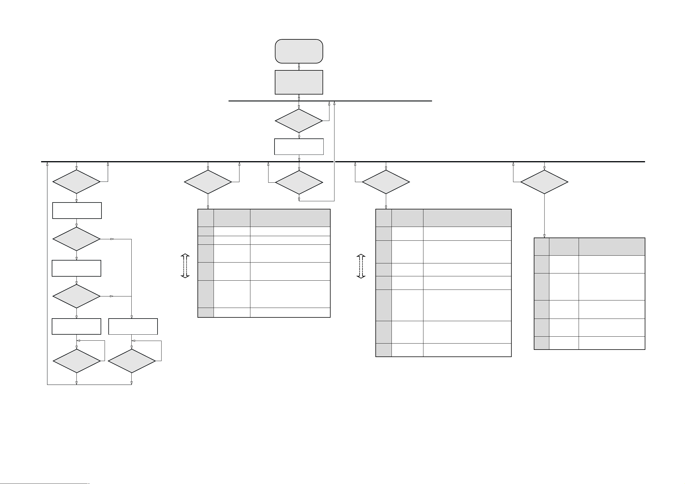
SERVICE TEST PROGRAM I
ADC
TEST
SEATING
Button pressed?
Y
9
Button pressed?
N
Display shows
"ADC Value"
(Ref Table 1)
To start service test program
hold DISC1 & STANDBY-ON
buttons depressed while
plugging in the mains cord*
Display shows the
ROM version
"S-Vyy"
* Hold till the Display is shown
S refers to Service Mode
V refers to Version
yy refers to Software version number of the uProcessor
(counting up from 01 to 99)
MAIN MENU
TUNER
TEST
N
Y
TUNING
Button pressed?
Y
Display Tuner Version
"ccc"
TUNING
Button pressed?
Y
N
N
QUARTZ
TEST
CLOCK-TIMER
Button pressed?
Y
Display shows
32K
Output at (Front Board)
pin 19 of uP = 2048Hz
CLOCK-TIMER
Button pressed?
N
N
DISPLAY
TEST
BII
Button pressed?
Y
Display shows Figure 1
and Standby LED is
Green
BII
Button pressed?
N
Figure 1
N
Y
N
Name
ADC1
ADC2
ADC3
ADC4
ADC5
Input line to
uProcessor IC
Key0
Key1
VU_IN
MUX_DET
Options
Has it reach
"ADC5 Value" ?
N
SEATING
Button pressed?
Y
Display shows next
"ADC Value"
(Refer Table 1)
Remarks
Return the value assign for each key button.
Return the value assign for each key button.
Varies according to the signal dc level
The set temperature is measured via this NTC
line, if lower than 69 the set goes into Standby.
Return the value assign for the different possible
options
Table 1
Note:
ADC Test is used for checking the ADC inputs to the microprocessor. The display
shows an ADC value between 0 and 255 for an input signal between 0 and 5V.
Service frequencies are
copied to the RAM (see Table 2)
Tuner works normally except:
PROGRAM button
pin 19 of uP = 2,929.6875Hz
Disconnect
Mains cord ?
Y
Service Mode left
PRESET
1
2
3
4
5
6
7
8
9
10
11
Note: * Depending on the selected grid frequency (9 or 10kHz).
By holding the "DISC5" and "STANDBY-ON" buttons depressed while switching on the Mains supply, one of the
undermentioned features will be activated:
- the tuning grid frequency is toggled between 9kHz and 10kHz for the Oversea (/21) version.
N
Europe
"EUR"
87.5MHz
108MHz
531kHz
1602kHz
558kHz
1494kHz
87.5MHz
87.5MHz
87.5MHz
87.5MHz
98MHz
USA
"USA"
87.5MHz
108MHz
530kHz
1700kHz
560kHz
1500kHz
98MHz
87.5MHz
87.5MHz
87.5MHz
87.5MHz
Y
Display shows
12M
Output at (Front Board)
9
Button pressed?
Y
Oversea
"OSE"
87.5MHz
108MHz
530/531kHz*
1700/1602kHz*
560/558kHz*
1500/1494kHz*
98/87.5MHz*
87.5MHz
87.5MHz
87.5MHz
87.5/98MHz*
Table 2
N
East Europe
"EAS"
87.5MHz
108MHz
531kHz
1602kHz
558kHz
1494kHz
87.5MHz
87.5MHz
87.5MHz
87.5MHz
98MHz
Y
Display shows Figure 2
and Standby LED is
RED
9
Button pressed?
Y
East Eur. Extended-band
"EAS"
65.81MHz
108MHz
74MHz
87.5MHz
531kHz
1602kHz
558kHz
1494kHz
98MHz
70.01MHz
65.81MHz
N
TEST
EEPROM TEST Some test patterns will be sent to the EEPROM.
TEST
AUTO STANDBY
TOGGLE
ROTARY
ENCODER TEST
LEAVE SERVICE
TEST PROGRAM
Figure 2
Activated with
T
9 to Exit
SEEPROM FORMAT
SUBW +
(Remote Control)
SOURCE / VOLUME
Knob
Disconnect
mains cord
Various
other Tests
ACTION
"PASS" is displayed if the uProcessor read back
the test patterns correctly, otherwise "FAIL" will be
displayed.
Load default data. Display shows "NEW" for 1 second.
Caution!
All presets from the customer will be lost!!
Pressing this button will toggle between the status
"AUTO STANDBY ON" and "AUTO STANDBY OFF".
The status will scroll once across the Display.
Display shows value for 2 seconds.
Values increases or decreases in steps of 1 until
0 (Min.) or 40 (Max.) is reached.
5DTC MX.. Range Service Test Program dd wk0302
3-2 3-2
SERVICE TEST PROGRAM II
DVD SVC MENU
2
DVD I
C
COMMUNICATION
TEST
MUTE
Button pressed?
Y
Send request for
DVD Software Version
2
C ports
via I
Is Back End
Software Version
Received?
Y
Display shows
"BEA-xxVxx"
Is 5DTC
Software Version
Received?
Y
Display shows
"5DTCx.x"
9
Button pressed?
N
N
N
Display shows
"FAIL"
N
Button pressed?
To start service test program
hold DISC1 & STANDBY-ON
buttons depressed while
MAIN MENU
plugging in the mains cord*
Display shows the
ROM version
"S-Vyy"
(Main menu)
* Hold till the Display is shown
S refers to Service Mode
V refers to Version
yy refers to Software version number of the uProcessor
(counting up from 01 to 99)
DVD SERVICE
TEST
DISC
Button pressed?
Y
Display shows
"DVD SVC"
N
Note:
1. Remote Control must be in DVD source before start of any DVD Service Test.
2. All buttons on this "DVD SVC" test refers to the buttons on the Remote control.
3. Awaits for the mechanism to initialized before performing DVD test.
DVD VERSION
MATRIX INFO
N
Choose step
by pressing
S
T
VOL +
Button pressed?
STEP
Choose step
by pressing
S
T
DIM
Button pressed?
Y
STEP
1
2
3
4
5
N
DISPLAY
SLASH ’###’
REGION ’#’
KARAOKE
or
NON KARA
V/O SCART
or
V/O PrPbY
TV - NTSC
or
TV - PAL
or
TV - AUTO
N
9
Button pressed?
Y
REMARKS
Slash version number
Region code setting (Number 1 - 6)
Karaoke feature
Video Output setting
TV system setting
Press
9
to exit
DVD Version Matrix Info is used to read the version matrix information
that are stored/defined in the DVD module software.
9
N
DVD PLAYER TEST
(with User interaction)
Y
DISPLAY
1
FEA-zzzz
2
TRAY
3
SLEDGE
4
MOTOR
5
FOC-RDL
FOC FAIL
RDL FAIL
GROOVES
6
ACTION
Returns the Front End Ali Servo Processor
software version.
BII
BII
BII
and
and
Tray 1 can be open or close with the
PROGRAM buttons repectively.
Insert a CD onto Tray 1 and close before
proceding to next test.
Sledge can be move in and out with the
and PROGRAM buttons respectively.
Dismotor is turn on and off by pressing
PROGRAM buttons repectively.
DVD Module does a Focus test follow by Radial
test if focus is successful.
Is displayed when the focus test fail.
Is displayed when the radial test fail.
In this test the laser spot can jumps to another
position.
BII
to jump to the next postion &
Press
PROGRAM to jump to the previous postion.
Disconnect mains cord to exit the Service Test
Program.
N
Button pressed?
DVD DEALER TEST
(without User interaction)
VOL -
Y
DVD Dealer Test is used to check the flash RAM,
the SDRAM CLOCK, the NVRAM and the I
communication (I2C NVRAM I2C DAC, I2C 5DTC
2
C SDPIF IC)
and I
STEP
1
2
3
4
DISPLAY
CHECKSUM
SDRAM CLK
NVRAM
2
C COMM
I
ACTION
Check the correctness of the
checksum in the flash. Display will
show "PASS" or "FAIL" accordingly.
Test the SDRAM clock output.
Display "PASS" or "FAIL"
accordingly.
Pro-Scan: 114MHz +/- 25ppm
Non Pro-Scan: 108MHz +/- 25ppm
Makes a write followed by a read
test to the NVRAM. Display will
show "PASS" or "FAIL" accordingly.
2
C bus to NVRAM, DAC,
Checks I
5DTC and SDPIF IC. Display will
show "PASS" or "FAIL" accordingly.
Disconnect mains cord to exit
the Service Test Program.
2
C
Y
Y
DVD I2C Communication Test is used to test the I2C communication
port between the DVD module and the microprocessor of the set.
5DTC MX.. Range Service Test Program dd wk0302

3-3
Reprogramming of DVD version matrix
Caution:
This information is confidential and may not be distributed. Only a qualified service person
should reprogram the mono BE board.
After replacement/repair of the Mono BE board, the customer settings and also the region code may be lost.
Reprogramming will put the set back in the state in which it has left the factory, i.e. with the default settings
and the allowed region code.
Reprogramming will be done by way of the Remote Control.
Put the player in stop mode, Disc 1 with no disc loaded.
Do the following steps with the Remote Control:
1) Press <DISC MENU> followed by numerical keys <1> <5> <9>
The set display shows: - 0 - 0 - 0 - 0 -
2) Press now successively the following numerical keys :
for MX3900D/37 : <1><1><4> <0><1><0> <0><0> US
for MX3910D/17 : <1><1><4> <0><1><0> <0><0> US
for MX3950D/37 : <1><1><4> <0><1><0> <0><0> US
for MX3960D/17 : <1><1><4> <0><1><0> <0><0> US
3) Press <DISC MENU> again. The set display will show: DONE .
Caution: The set needs about 3 seconds to reset to required setting.
4) Disconnect mains to ensure proper reset.
Procedure for check Software version
1) Select Disc with the Remote Control
2) Press <SYSTEM MENU>
3) Use the down key move all the way down (4x) to
bottom of "Setup Menu".
4) Use the right key move to the sub-menu.
5) Use the down key move down (3x) to "Default" and
down one more time to see the software version.
6) The TV screen will shows:
1000 BEA3131PV08 R2812 V72
R
where 1000 = DVD version matrix (Region, Karaoke
Yes/No, Default Video O/P, Default TV
system)
31V08 = BE software version
2812 = FE software version
72 = 5DTC servo version
7) Press <OK> three times to exit.
Procedure to upgrade software
1) Power up the set and open tray Disc 1.
2) Place upgrade CD-ROM onto tray and close.
3) The set will display "DOWNLOAD" while the TV screen
4) Tray Disc 1 should then open.
5) The whole process should last for less than 2 minutes.
will shows:
Reading --> Update BEA --> Writing --> Done -->
Update FEA --> FEA Finish --> Unload Disc 1
Remove the upgrade CD-ROM and unplug the Mains
supply.
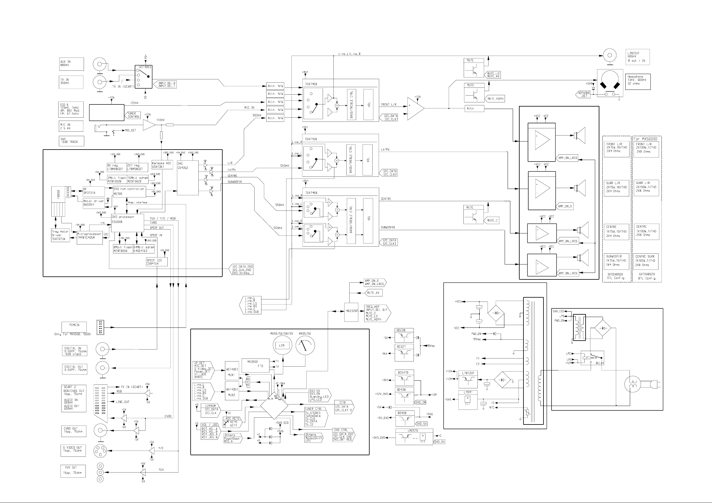
SET BLOCK DIAGRAM
4-1 4-1
ECO 6
DVD Module
Power Amplifier
TDA8920
L/R
POWER AMP
TDA8920
SURROUND
POWER AMP
1/2XTDA8920
1/2XTDA8920
Front Display
Mains and Regulator
MAINS TRAFO
LPS COIL
ECO Standby
TMP88CU74F
Note: All others are in the AV board.
MX3900D_130_wk302-2
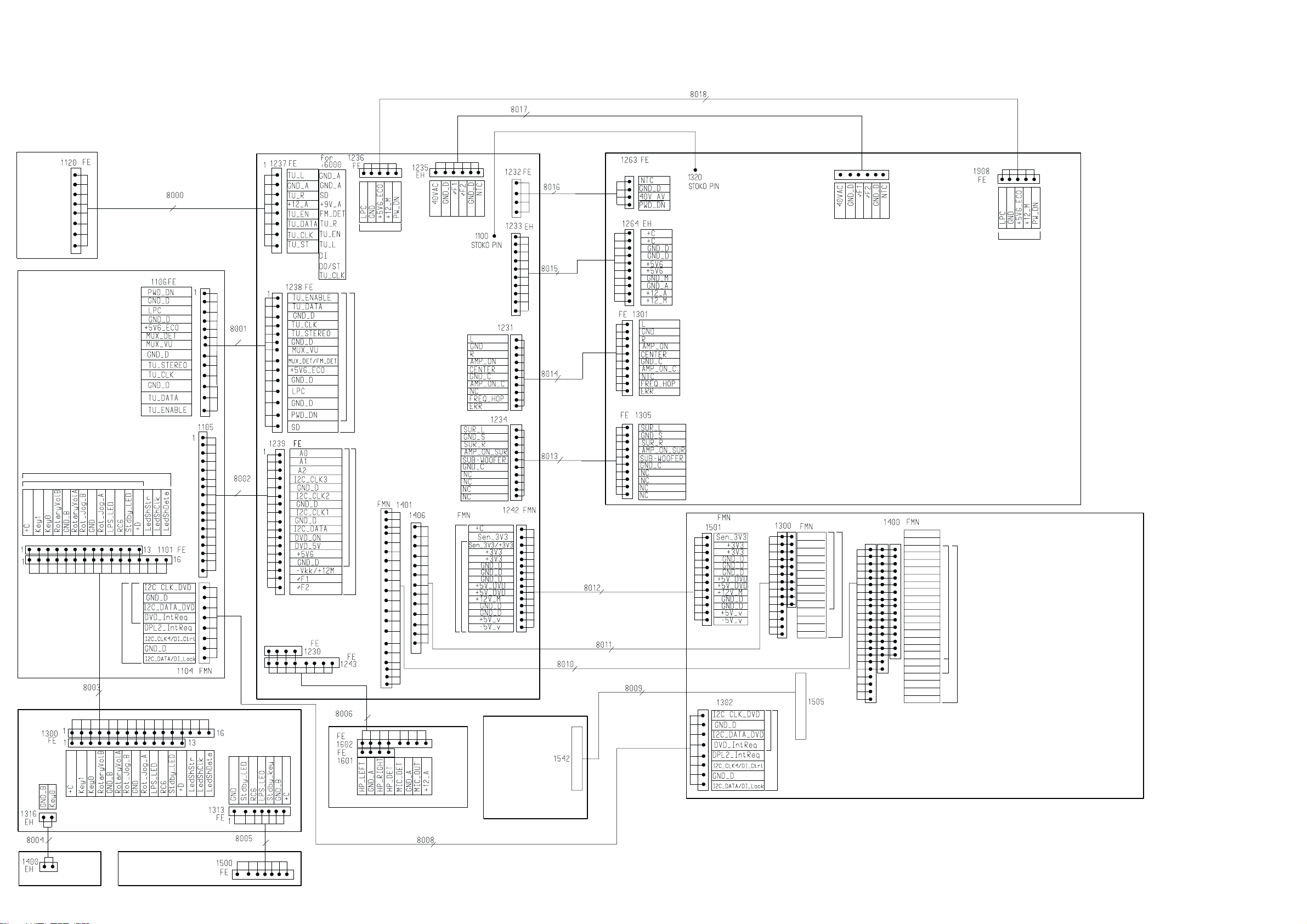
MAIN WIRING DIAGRAM
5-1
5-1
TUNER
AD
140mm
EH
240mm
1
8P
for ECO SET ONLY
1
AD
180mm
4P
EH
10P
180mm
1
1
AV
1
1
BD
400mm
Prefold
13P
for MX39/55/56/58/59
for i6000
FE
BD
10P
180mm
Prefold
1
FE
5PAD120mm
1
for ECO SET ONLY
POWER MODULE
Refer to page 5-2 for details
FRONT DISPLAY
MX55/56/58/59
MX3900D
MX39/55/56
MX58/59
AD
13P
100mm
AD
400mm
Prefold
17P
for MX55/56/58/59
1
AD Prefold
1
1
1
for MX3900D
4P 340mm (non K’ok)
8P 340mm (K’ok)
BD
180mm
10P
Prefold
1
1
1
13P 180mm (MX39/55/56)
13P 220mm (MX58)
Prefold AD
for MX39/55/56/58/59
for i6000
10P 280mm (MX39/55/56)
14P 220mm (MX58)
Prefold AD
Prefold AD
16P/18P(K’ok) 180mm (MX39/55/56)
22P 220mm (MX58)
16P 220mm (MX59)
FLT
40P
FFC
40P
AD
280mm
1
13
FMN
PCMCIA
1
14
MX39/55/56
MX58/59
10
SCART 0
Mute_AV
GND_V
R_Pr
GND_V
C_B_Pb
GND_V
Y_G_Y
GND_V
CVBS
GND_V
Y
GND_V
C
40P
FLT
for MX5800SA
for MX3900D
1
22
DVD_SC
1
1
GND_Sc
DVD_L
GND_L
DVD_R
GND_R
DVD_SUB
GND_SUB
DVD_Ls
GND_S
DVD_C
GND_C
DVD_Rs
GND_S
GND_d
DIG_OUT
DIG_IN_1
DIG_IN_2
GND_MIC
16
MIC_IN
18
GND_a
DPL2_R
GND_a
DPL2_L
MX39/55/56/59
MX5800SA
K’ok
DVD Module
Refer to page 5-3
for details
HDPH & MIC
1
2P
220mm
FRONT CONTROL
DTC
KEY
POWER SWITCH
Prefold
AD
7P
340mm
AD
4P 220mm (MX39/55/56)
8P 220mm (MX58/59)
for MX5500/5600
5-2 5-2
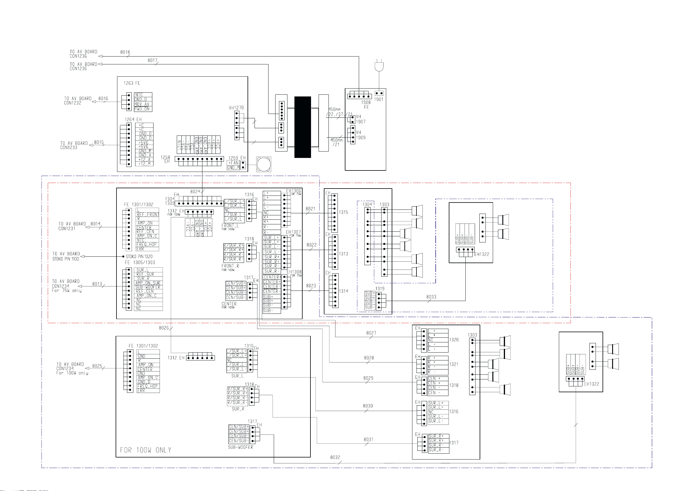
WIRING DIAGRAM - POWER MODULE DETAILS
4P
10PEH220mm
10P
180mm
Prefold
180mm
10P
Prefold
180mm
BD
BD
AD
5PAD120mm
1
1
1
1
240mm
EH
SUPPLY
Amplifier
3104 213 3525
1
EH 10P 280mm
1
1
TRAFO
1
NOTE :
1
VH 3X
150mm
Blue/Yellow
Red/Black
VH 3X
150mm
FAN
1
1
EH 9P
1
1
1
1
1
120mm
EH 8P
120mm
EH 8P
120mm
1
MAINS
and
ECO STBY
1
1
1
10
1
2
3
4
5
6
7
8
9
SPK I
1
1
2
3
4
5
6
7
8
9
10
11
12
75W
1
SUR L
SUB-WOOFER
1
6-CHANNEL
CENTER
75W 6-CHANNEL : 1 X CLASS-D AMPLIFIER + SPK I
75W 7-CHANNEL : 1 X CLASS-D AMPLIFIER + SPK I + SPK II
100W : 2 X CLASS-D AMPLIFIER + SPK I + SPK II
L
R
SUR R
EH 4P 120mm
SPK II
SUB-WOOFER_R
SUB-WOOFER_L
1
75W 7-CHANNEL
10P
Prefold
1
BD
220mm
Amplifier
3104 213 3525
EH 6P
120mm
SPK I
1
EH 5P
120mm
1
EH 4P
1
1
1
EH 4P 220mm
120mm
EH 4P
120mm
EH 4P
140mm
EH 5P
180mm
1
1
1
1
1
1
2
3
4
5
6
7
8
9
10
L
R
CENTER
SUR L
SUR R
SPK II
SUB-WOOFER_R
SUB-WOOFER_L
1
100W

5-3 5-3
WIRING DIAGRAM - DVD MODULE DETAILS
TO AV BOARD
CON1242
TO AV BOARD
CON1401
TO FRONT DISPLAY
CON1104
1
1
1
FMN 1501
+3V3_SENSE
+3V3
+3V3
GND_D
GND_D
GND_D
+5V
FMN 1401/1402
7401-A
L_GND
7401-B
R_GND
7402-A
LFE_GND
DVD_LS / 7402-B
FMN 1301
CD222 BE
GND_D
HDASP
HCS3
HSC1
HA2
HA0
HPDIAG
HA1
HCS16
HIRQ
GND_D
NC
C_det
HIORDY
GND_D
HRD
GND_D
HWR
GND_D
Card_On
+5D
GND_D
HD15
HD0
HD14
HD1
HD13
HD2
HD12
HD3
HD11
HD4
HD10
HD5
HD9
HD6
HD8
HD7
GND_D
IDE_RST
GND_D
HDASP
HCS3
HSC1
HA2
HA0
HPDIAG
HA1
HCS16
HIRQ
GND_D
+5D
P28_1
HIORDY
GND_D
HRD
GND_D
HWR
GND_D
HDRQ
NC
GND_D
HD15
HD0
HD14
HD1
HD13
HD2
HD12
HD3
HD11
HD4
HD10
HD5
HD9
HD6
HD8
HD7
GND_D
IDE_RST
1
TO AV BOARD
CON1405
TO 5DTC MECH ASSY
TO 5DTC MECH ASSY
CD222 FE
PH 1106
1
FMN 1503
1
FMN 1302
1
1
GND_D
HDASP
HCS3
HSC1
HA2
HA0
HPDIAG
HA1
HCS16
HIRQ
GND_D
+5D
P28_1
HIORDY
GND_D
HRD
FMN 1107
1
GND_D
HWR
GND_D
HDRQ
NC
GND_D
HD15
HD0
HD14
HD1
HD13
HD2
HD12
HD3
HD11
HD4
HD10
HD5
HD9
HD6
HD8
HD7
GND_D
IDE_RST
Optical
Lightpen
5DTC Mech Assy
Control Board
FMN 1802
1
TO PCMCIA
CON1542
TO 5DTC MECH ASSY

6-1
2G
4G
1G
5G
3G
7G
6G
8G
9G
10G
12G
13G
1G
(2G - 10G)
1G - 13G)
(1G)
Dp
col
10
6-1
FTD DISPLAY PIN CONNECTIONS
FRONT BOARDS
TABLE OF CONTENTS
FTD Display pin connection ............................................ 6-1
Front Display part - Circuit diagram ................................ 6-2
Front Display part - Component & Chip layout................ 6-3
Front Control part - Circuit diagram ................................. 6-4
Front Control part - Component & Chip layout................ 6-5
Power Switch and DTC Key parts ................................... 6-6
HDPH & Mic parts ...........................................................6-7
Electrical parts list ........................................................... 6-8
P1
P2
P3
P4
P5
P6
P7
P8
P9
P10
P11
P12
P13
P14
P15
P16
P17
P18
P19
P20
1G
1G
2G
11G
A
B
D
C
B
A
C
D
E
C
D
A
B
(1G)
2G
j , p
m
A
B
C
D
E
3G
a
h
j , p
k
b
f
g
c
e
r
n
d
-
-
-
-
-
4G
a
h
k
b
f
m
g
c
e
r
n
d
-
-
-
-
-
a
h
j , p
k
b
f
m
g
c
e
r
n
d
-
-
-
-
-
3G
j , p
4G
f
g
r
e
(2G - 10G)
5G
a
h
k
b
f
m
g
c
e
r
n
d
-
-
-
-
-
-
-
5G
6G
12G
a
j
h
b
k
m
col
c
n
p
d
Dp
7G
8G
9G
10G
13G
1
9
8
10
7
6
2
3
4
5
(11G - 13G)
6G
j , p
m
col
7G
a
h
j , p
k
b
f
m
g
c
e
r
n
d
-
-
-
-
8G
a
h
k
b
f
g
c
e
r
n
d
-
-
-
-
-
-
a
h
j , p
k
b
f
m
g
c
e
r
n
d
col
Dp
-
-
-
9G
j , p
10G
a
h
j , p
k
b
f
m
g
c
e
r
n
d
-
-
-
-
-
11G
SL1
a
SL2
h
SL3
SL4
k
SL5
b
SL6
f
SL7
m
SL8
g
SL9
c
SL10
e
r
n
d
L10
12G
C1
C2
C3
C4
C5
C6
C7
C8
C9
C10
SUB1
L1
SUB2
L2
SUB3
L3
SUB4
L4
SUB5
L5
SUB6
L6
SUB7
L7
SUB8
L8
SUB9
L9
SUB10
13G
SR1
SR2
SR3
SR4
SR5
SR6
SR7
SR8
SR9
SR10
R1
R2
R3
R4
R5
R6
R7
R8
R9
R10
FTD DISPLAY PIN NO.
FUNCTION
FTD DISPLAY PIN NO.
FUNCTION
3
1
19
12
1
9
8
P
P
18
4
4
7
6
13
G
G
17
1
1
0
2
P
P
P
16
15
4
4
5
9
8
0
N
N
N
P
X
P
3
1
2
N
F
F
F
P
2
2
2
4
4
3
4
2
1
9
0
8
7
5
6
G
G
G
G
7
5
N
P
N
X
20
P
4
4
4
4
5
3
10
11
9
G
G
G
6
4
14
1
1
1
3
4
P
P
13
5
5
1
2
F
F
1
1
12
1
1
5
7
6
P
N
N
X
X
5
3
F
1
2
1
1
0
9
8
N
N
N
X
X
X
Note: Fn : Filament pin
2
2
2
2
3
1
2
4
P
N
N
P
11
X
X
10
nG : Grid pin
Pn : Anode pin
NP : No Pin
MX : No extended pin
2
2
2
2
3
3
3
3
2
5
7
8
9
0
6
P
P
P
P
9
7
6
8
1
P
P
P
5
4
3
3
2
3
4
P
P
N
2
1
X
3
3
3
8
7
5
6
4
3
1
2
G
G
G
G
6-2
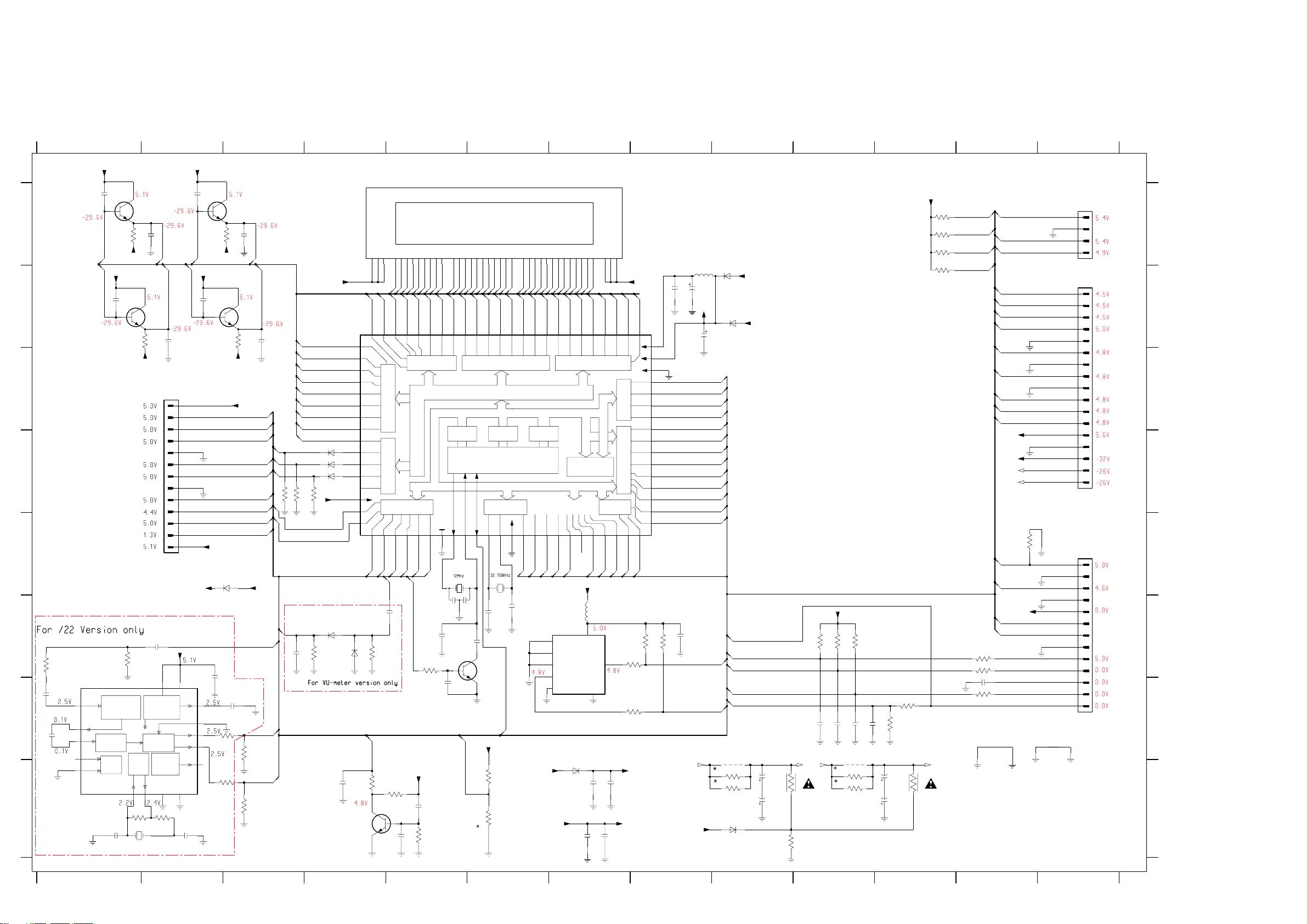
FRONT DISPLAY PART - CIRCUIT DIAGRAM
6-2
A
B
C
D
G
H
E
F
1100 A8
1101 C2
1104 A13
1105 B13
3108
2104
2128
1106 E13
2101 F3
2102 F2
2103 F2
2104 G1
2105 G3
2106 H1
2107 H2
2108 F6
2109 F6
2110 F5
2111 F8
2112 F5
2113 G5
2114 H4
2115 H7
2116 H7
2117 H5
2118 H5
2119 H7
2120 H7
2121 G12
2122 G10
2123 G10
2124 G10
2125 G11
2126 H9
2127 H11
2128 G1
2129 H11
2130 B8
2131 B8
2132 B8
2133 A1
2134 A2
2135 A2
2136 A3
2137 B1
2138 B2
2139 B2
2140 B3
2141 F4
2142 H9
3105 F4
3106 F4
3107 F1
3108 F1
3109 G3
3110 G3
3111 H3
3112 H3
3113 H1
3114 H2
3115 F8
3116 F8
3117 F8
3118 F5
3119 G8
3120 G9
3121 H10
3122 H6
3123 H9
3124 H10
3125 H4
3126 H9
3127 H11
3128 H9
3129 H10
3130 H5
3131 H6
3132 H5
3133 H9
3158 F10
3159 F10
3160 F10
3161 F12
3162 F12
3163 G12
3164 G11
3165 G11
3166 A1
3167 A2
3168 B1
3169 B3
3170 A11
3171 A11
3172 A11
3173 B11
3174 D3
3175 D3
3176 D4
3177 E12
5100 B8
5102 E5
5103 E6
5104 F7
5105 H1
6100 D4
6101 D4
6103 D4
6105 F4
6106 H7
6107 H9
6108 B9
6113 B9
6118 F4
6119 E3
7103 F7
7104 F6
7105 H4
7106 A1
7107 A3
7108 B2
7109 B3
12345678910111213
GG1
1101
5
6
GG12
2138
+D
HN-13LM05T
3164
100K
22K
3127
47R
+E
3170
10K
3171
10K
3172
10K
3173
10K
-F2-F1
TU_GND
I2C_Clk_DVD
I2C_Data_DVD
I2C_Clk2
I2C_Clk3
3161
3162
GND_B
1K0
1K0
100p2121
1K03163
I2C_Clk_DVD
I2C_Data_DVD
DVD_IntReq
A0
A1
A2
I2C_Clk3
I2C_Clk2
I2C_Clk1
I2C_Data
DVD_On
DVD_5V
+5V6
-Vkk
F1
F2
PowerDown
LPC
+5V6_ECO
MUX_DET
MUX_VU
TU_GND
3177
1M0
1104
1
2
3
4
FMN
1105
1
2
3
4
5
6
7
8
9
10
11
12
13
14
15
16
17
FE-ST-VK-N
1106
1
2
3
4
5
6
7
8
9
10
11
12
13
FE-ST-VK-N
22p
2135
7107
BC847B
1100
82K
22p
3167
2136
F2c
F2a1F2b
P20
-Vkk
100n
2u2
2105
3169
3109
7109
BC847B
82K
-Vkk
+C
RotaryVolB
RotaryVolA
Rot_Jog_B
Rot_Jog_A
LPS_LED
Stdby_LED
TuRdsClk
3110
TuRdsData
10K
GG11
2140
Key1
Key0
RC6
+5V6
TuRDS
GG13
22p
LPS_LED
Stdby_LED
AUX_SEL
3174 10K
Rot_Jog_A
TMP88CU74F
P12
P13
P14
P15
P16
P17
P18
P19
P20
6103
6100
6101 1N4148
10K
3175
3176
DVD_5V
VU_IN
3105
2101
220n
-F2
1N4148
1N4148
10K
-Vkk
6105
BAS316
470K
7100
2114
65
V24
66
V25
V26
67
68
V27
69
V28
V29
70
V30
71
72
V31
73
V32
74
V33
75
V34
76
V35
77
V36
VKK
78
-SCK1
79
SI1
6118
BAT54 COL
10n
1
3106
3125
G11
G13
22p
2139
22p
1
2
3
4
5
GND_B
6
7
8
9
10
11
12
13
+E
6119
+E
1N4003
+D
12
2103
VREF
3
SYNC
10
RDCL
16
RDDA
QUAL
1K0
2
1
3111
1K0
11
10K
2107
47p
3112
7105
BC847B
2
3
P10
P11
V21
V23
V22
8-Bit h. breakdown v.
out. port w. latch P9
PD
5-Bit h. breakd. v.
out w. latch
8-Bit Input/Output
(tri-state)
P04
P03
SO1
3
RotaryVolA
Rot_Jog_B
MUX_VU
2141
10K
Reset
1K0
3130
680K
P19
7
9
8
P18
P19P2P20
P8
P9
V20
8-Bit h. break. v.
80k pull
down
source open
drain 80k p.d.
P05
4
RotaryVolB
I2C_Clk2
1u0
10n
2118
P15
P16
P17
P7
V19
P0
P06
LPC
MpOscShift
3118
4K7
+C
2117
3132
470n
680K
P1024P1123P1215P1314P1413P1512P1611P1710P18
25
P11
P12
P13
P14
P10
P5
P4
P6
V18
P07
I2C_Clk1
P3
V16
V15
V17
8-Bit high breakdown voltage 8-Bit high breakdown v.
output port with latch output port with latchout w. latch P8
VFT driver circuit (automatic display)
XIN
XOUT
VSS
7
8809
10 11 12 13 14 15 16 17 18 19220 21 22 23 24
5102
2p2
2110
2112
33p
2113
Options
P7
P826P9
28
27
P2
V14
sink o.
-RESET
22p
7104
BC847B
3122
3131
P5
P6
30
29
P1
V12
V13
ROMRAM
CPU
8-Bit I/O P2
sink o.drain
XTIN
XTOUT
5103
32K768
22p
2109
+C
2K7
1K8
P3P4P5P6P7P8P9
G1
P331P4
32
2108
Reset
P2
V11
TEST
22p
P1
1G
352G363G374G385G396G407G418G429G43
33
GG1G2G3G4G5G6G7G8G9
P1
G3
G4
G2
V9
V10
P7 P6
80k pull down80k pull down
P6-P9 source open drain
Program
Counter
drain
-STOP
-INT0
MpOscShift
I2C_Data
G7
G6
G5
V6
V7
V8
8-Bit Input/Output
(tri state)
TC2
-INT1
-DV0
TuCE
TuStereo
TuRdsClk
7103
M24C02
1
E0
2
E1
3
E2
6
SCL
7
WC_
6106
+5V6
1N4003
10G4511G
44
G10
GG11
GG12
G8
V5
8-Bit A/D
Converter
P1
TC4
5104
VCC
VSS
2119
F1c
12G4613G
47
52
51
GG13
G9
G10
V4
V3
80k pull down
3-B. I/O P3
( tristate )
INT2
TC1
PowerDown
DVD_IntReq
+D
2u2
8
5
SDA
4
2115
100n
2116
100n
2120
F1a53F1b
-F1
G13
G12
G11
41424344454647484955051525354555657585966061626364
V1
V0
V2
VDD
VAREF
VASS
AIN13
P5
AIN12
AIN11
AIN10
4-Bit In/Output
(tri-state)
AIN7
P4
AIN6
AIN5
AIN4
AIN3
8-Bit Input/Output
AIN2
(tri-state)
AIN1
AIN0
-SCKO
INT4
SCA
SCL
I2C_Clk_DVD
I2C_Data_DVD
RC6
3117
1K0
3119
1K0
+D
100n
+5V6+5V6
100n
3115
40
39
38
37
36
35
34
33
32
31
30
29
28
27
26
25
10K
3116
2130
GND_B
2111
10K
100n
2131
GND_B
1u0
F1
-Vkk
5100
2u2
47u
+C
47u
TuRdsData
TuData
TuClk
MUX_DET
VU_IN
Options
DVD_On
I2C_Clk3
I2C_Data
I2C_Clk1
6108
+5V6_ECO
BAS316
6113
+5V6
1N4003
2132
A0
A1
A2
Key1
Key0
DC Voltage measured in DISC Mode PLAY
* Provision in layout only
TuRDS
TuStereo
TuClk
TuData
TuCE
3120
3123
10R
2126
2142
4u7
4u7
3126
3133
47R
22K
10R
3128
6107
BZX79-B5V6
3158
100p
+E
10K
10K
10K
3160
3159
2124
100p
2125
2127
2129
3165
4u7
4u7
100p
100p
2123
2122
3121
F2
10R
3124
10R
3129
8239 210 94112 dd 20 Jan 2003
1K5
560p
560p
7102
SAA6581T
4
MPX
SCOUT
8
CIN
7
15
TCON
MODE
9
+D
22p
2133
CLOCKED
7106
BC847B
82K
22p
3166
2134
-Vkk
G1
+D +D
G12
22p
2137
57 Khz
BANDPASS
(8th ORDER)
COMP
TEST
CTRL
2106
82p
3107
To Front Control
OSC
CLK
OSCI
13
3113
220K
5105
AT-51
3168
10K
VSSA
&
OSCO
7108
BC847B
82K
-Vkk
FE-ST-VK-N
2102
1n0
VDDA VDDD
POW SUPPL
&
RESET
RDS/RBDS
DEM
SIGNAL
QUALITY
DET
VSSA VSSD
14
3114
2K2
A
To CD222 BE
B
C
To AV Board
D
E
F
To AV Board
G
H
12345678910111213
6-2a
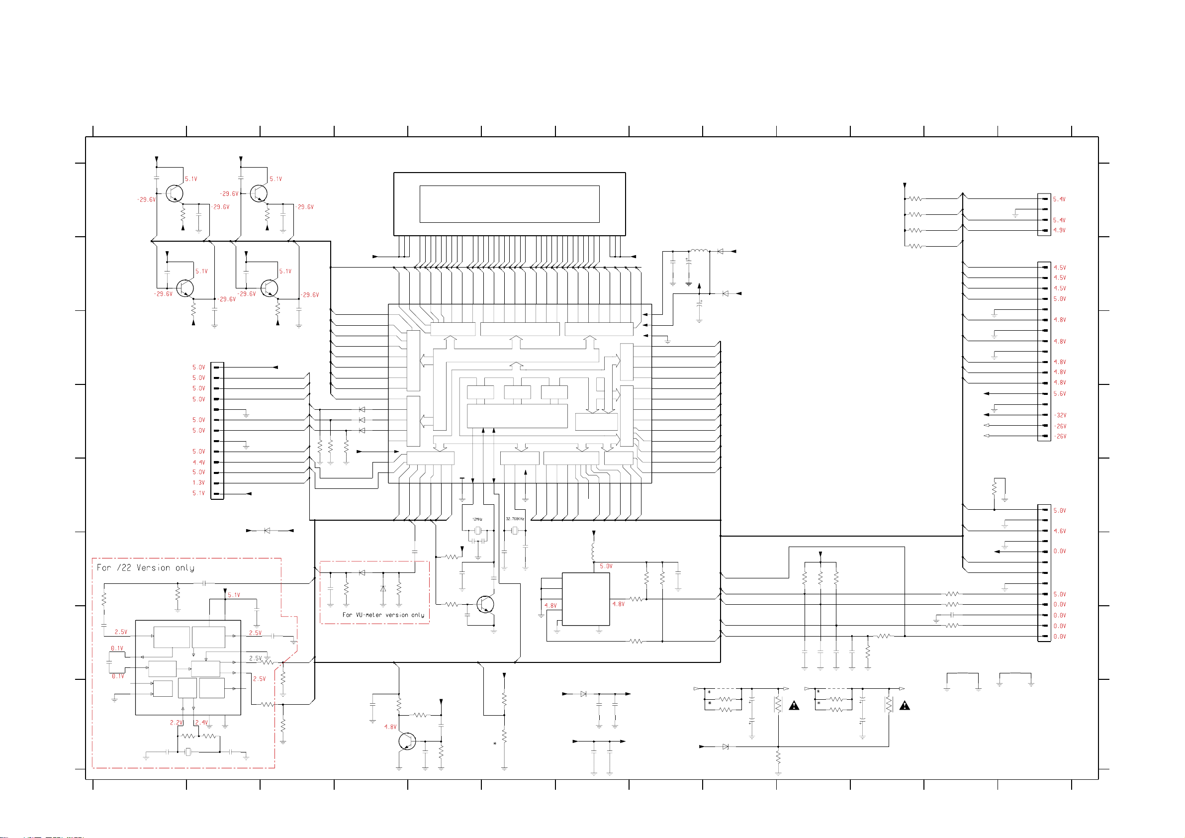
FRONT DISPLAY PART - CIRCUIT DIAGRAM (For pt 4 board)
6-2a
A
B
C
D
G
H
E
F
1101 C2
1104 A13
1105 B13
1106 E13
3108
2104
2128
2101 F3
2102 F2
2103 G2
2104 G1
2105 G3
2106 H1
2107 H2
2108 F6
2109 F6
2110 F5
2111 F8
2112 F5
2113 G5
2114 H4
2115 H7
2116 H7
2117 H5
2118 H5
2119 H7
2120 H7
2121 G12
2122 G10
2123 G10
2124 G10
2125 G11
2126 H9
2127 H11
2128 G1
2129 H11
2130 B8
2131 B8
2132 B9
2133 A1
2134 A2
2135 A2
2136 A3
2137 B1
2138 B2
2139 B2
2140 B3
2141 F5
2142 H9
3105 F4
3106 F4
3107 F1
3108 F1
3109 G3
3110 G3
3111 H3
3112 H3
3113 H2
3114 H2
3115 F8
3116 F8
3117 F8
3118 F5
3119 G8
3120 H9
3121 H10
3122 H6
3123 H9
3124 H10
3125 H4
3126 H9
3127 H11
3128 H9
3129 H10
3130 H5
3131 H6
3132 H5
3133 H9
3158 F10
3159 F10
3160 F10
3161 F12
3162 F12
3163 G12
3164 G11
3165 G11
3166 A1
3167 A3
3168 B2
3169 B3
3170 A11
3171 A11
3172 A11
3173 B11
3174 D3
3175 D3
3176 D4
3177 E12
3201 F5
5100 B8
5102 E5
5103 E6
5104 F7
5105 H2
6100 D4
6101 D4
6103 D4
6105 F4
6106 H7
6107 H9
6108 B9
6113 B9
6118 F4
6119 E3
7103 F7
7104 F6
7105 H4
7106 A1
7107 A3
7108 B2
7109 B3
1 2345678910111213
GG1
2138
1101
5
6
GG12
+D
22p
1
2
7
8
9
11
12
13
VREF
SYNC
RDCL
RDDA
QUAL
11
2107
3
4
5
6
10
12
47p
G13
+D
2135
+E
G11
3
10
16
2
1
22p
2139
GND_B
22p
+E
1N4003
2103
3167
-Vkk
6119
100n
1K0
3111
1K0
7107
BC847B
2u2
2105
3109
82K
3169
+C
2136
7109
BC847B
82K
-Vkk
RotaryVolB
RotaryVolA
Rot_Jog_B
Rot_Jog_A
LPS_LED
Stdby_LED
TuRdsClk
3110
TuRdsData
3112
22p
GG11
TuRDS
10K
10K
GG13
2140
Key1
Key0
RC6
+5V6
22p
LPS_LED
Stdby_LED
AUX_SEL
10K
3175
3174
DVD_5V
Rot_Jog_A
2101
VU_IN
-F2
7100
TMP88CU74F
P12
P13
P14
P15
P16
P17
P18
P19
P20
1N4148
6103
1N4148
6100
1N4148
6101
10K
10K
3176
-Vkk
6105
BAS316
3105
470K
220n
2114
65
V24
66
V25
67
V26
68
V27
V28
69
V29
70
71
V30
72
V32
73
V33
74
75
V34
76
V35
77
V36
VKK
78
-SCK1
79
SI1
6118
BAT54 COL
10n
7105
BC847B
V31
1
3106
3125
F2a1F2b
2
P11
V23
SO1
Rot_Jog_B
10K
Reset
HN-13LM05T
F2c
P19
P20
9
8
7
3
P17
P18
P19P2P20
P8
P9
P10
V21
V20
V22
8-Bit h. break. v.
80k pull
down
8-Bit h. breakdown v.
out. port w. latch P9
PD
source open
drain 80k p.d.
5-Bit h. breakd. v.
out w. latch
8-Bit Input/Output
(tri-state)
P03
P04
P05
3
4
RotaryVolB
RotaryVolA
I2C_Clk2
MUX_VU
MpOscShift
1u0
2141
+C
1K0
3130
680K
10n
2118
P1024P1123P1215P1314P1413P1512P1611P1710P18
25
P12
P13
P14
P15
P16
P7
V19
P0
P06
LPC
P10
P11
P5
P4
P6
V16
V17
V18
P07
I2C_Clk1
V15
8-Bit high breakdown voltage 8-Bit high breakdown v.
output port with latch output port with latchout w. latch P8
VFT driver circuit (automatic display)
XIN
XOUT
VSS
8809
7
5102
+E
3201
10K
2p2
2110
3118
4K7
33p
2113
2117
470n
3132
680K
F1c
P826P9
29
28
27
P1
P2
P3
V13
V14
1G
33
32
30
352G363G374G385G396G407G418G429G43
P3P4P5P6P7P8P9
P1
GG1G2G3G4G5G6G7G8G9
G2
G1
G3
V11
V10
V12
P7 P6
80k pull down80k pull down
P6-P9 source open drain
ROMRAM
G4
V8
V9
Program
Counter
G5
CPU
8-Bit I/O P2
sink o.drain
XTIN
XTOUT
TEST
drain
-STOP
MpOscShift
8-Bit Input/Output
(tri state)
-INT0
-INT1
TuRdsClk
I2C_Data
sink o.
-RESET
10 11 12 13 14 15 16 17 18 19220 21 22 23 24
G6
V7
TC2
TuStereo
G7
V6
-DV0
TuCE
10G4511G
44
G10
GG11
G8
V5
8-Bit A/D
Converter
P1
TC4
P1
P2
P331P4
P5
P6
P7
12G4613G
47
51
GG12
GG13
G9
G10
V4
V3
80k pull down
3-B. I/O P3
( tristate )
INT2
TC1
PowerDown
DVD_IntReq
F1a53F1b
52
G11
V2
4-Bit In/Output
8-Bit Input/Output
INT4
RC6
5103
6106
1N4003
5104
VCC
2119
8
VSS
2115
+D
2u2
SDA
4
100n
100n
2120
5
2116
100n
+5V6+5V6
100n
22p
2112
Options
32K768
7104
BC847B
+C
3122
3131
2109
2K7
1K8
22p
2108
Reset
22p
+5V6
7103
M24C02
1
E0
2
E1
3
E2
6
SCL
7
WC_
1100
-F1
G12
G13
41424344454647484955051525354555657585966061626364
V1
V0
VDD
VAREF
VASS
AIN13
P5
AIN12
AIN11
AIN10
(tri-state)
AIN7
P4
AIN6
AIN5
AIN4
AIN3
AIN2
(tri-state)
AIN1
AIN0
-SCKO
SCA
SCL
I2C_Clk_DVD
I2C_Data_DVD
3115
3117
1K0
3119
1K0
+D
40
39
38
37
36
35
34
33
32
31
30
29
28
27
26
25
10K
+E
1
2
3
4
1
2
3
4
5
6
1104
FMN
1105
2130
100n
2131
GND_B
5100
2u2
47u
+C
47u
6108
BAS316
1N4003
2132
6113
+5V6_ECO
+5V6
3170
10K
3171
10K
3172
10K
3173
10K
I2C_Clk_DVD
I2C_Data_DVD
I2C_Clk2
I2C_Clk3
I2C_Clk_DVD
I2C_Data_DVD
DVD_IntReq
A0
A1
A2
I2C_Clk3
I2C_Clk2
7
GND_B
TuRdsData
TuData
TuClk
A0
A1
A2
MUX_DET
VU_IN
Options
DVD_On
Key1
Key0
I2C_Clk3
+E
1u0
2111
10K
3116
F1
-Vkk
I2C_Data
I2C_Clk1
TuRDS
TuStereo
TuClk
TuData
TuCE
3120
3123
10R
3128
6107
BZX79-B5V6
10R
2126
2142
4u7
4u7
3126
3133
22K
10K
3159
3160
10K
3158
10K
3164
22K
2124
100p
2125
2127
2129
3165
4u7
4u7
100K
3127
47R
100p
100p
100p
2123
2122
3121
F2
10R
3124
10R
3129
DC Voltage measured in DISC Mode PLAY
47R
-F2-F1
TU_GND
GND_B
* Provision in layout only
3161
3162
1K0
1K0
100p2121
1K03163
I2C_Clk1
I2C_Data
DVD_On
DVD_5V
+5V6
-Vkk
F1
F2
1M0
3177
PowerDown
LPC
+5V6_ECO
MUX_DET
MUX_VU
TU_GND
8239 210 94114 ..3502p4 dd wk0404
8
9
10
11
12
13
14
15
16
17
FE-ST-VK-N
1106
1
2
3
4
5
6
7
8
9
10
11
12
13
FE-ST-VK-N
1K5
560p
560p
7102
SAA6581T
MPX
4
SCOUT
8
CIN
7
15
TCON
MODE
9
+D
22p
2133
CLOCKED
7106
BC847B
22p
82K
3166
2134
-Vkk
G1
+D +D
G12
22p
2137
57 Khz
BANDPASS
(8th ORDER)
COMP
TEST
CTRL
2106
82p
7108
BC847B
82K
3168
-Vkk
To Front Control
FE-ST-VK-N
2102
1n0
10K
3107
VDDA VDDD
POW SUPPL
&
RESET
VSSA
RDS/RBDS
DEM
SIGNAL
OSC
QUALITY
&
DET
CLK
VSSA VSSD
OSCO
OSCI
13
14
3113
3114
220K
2K2
5105
AT-51
A
To CD222 BE
B
C
To AV Board
D
E
F
To AV Board
G
H
1 2345678910111213
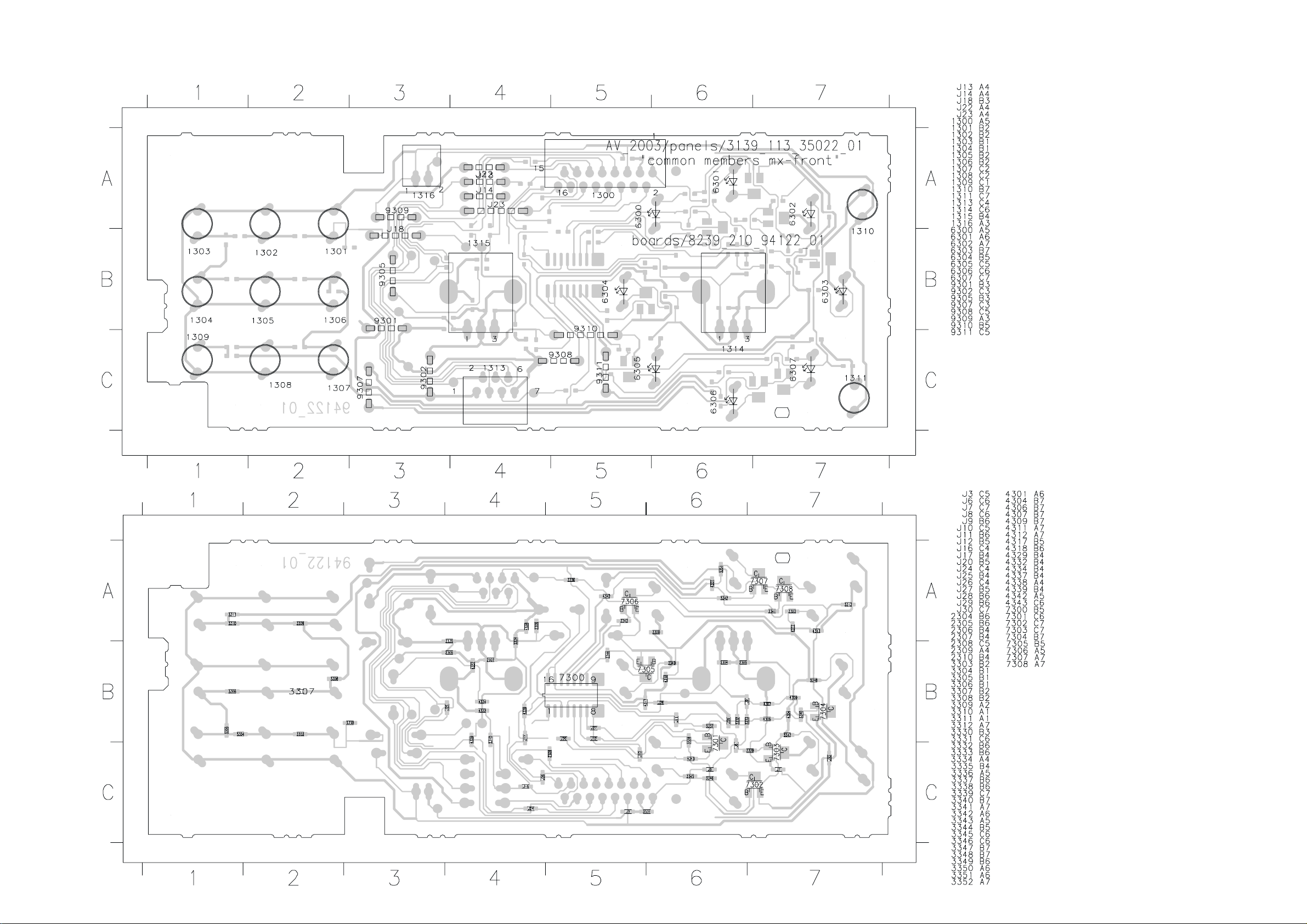
6-3 6-3
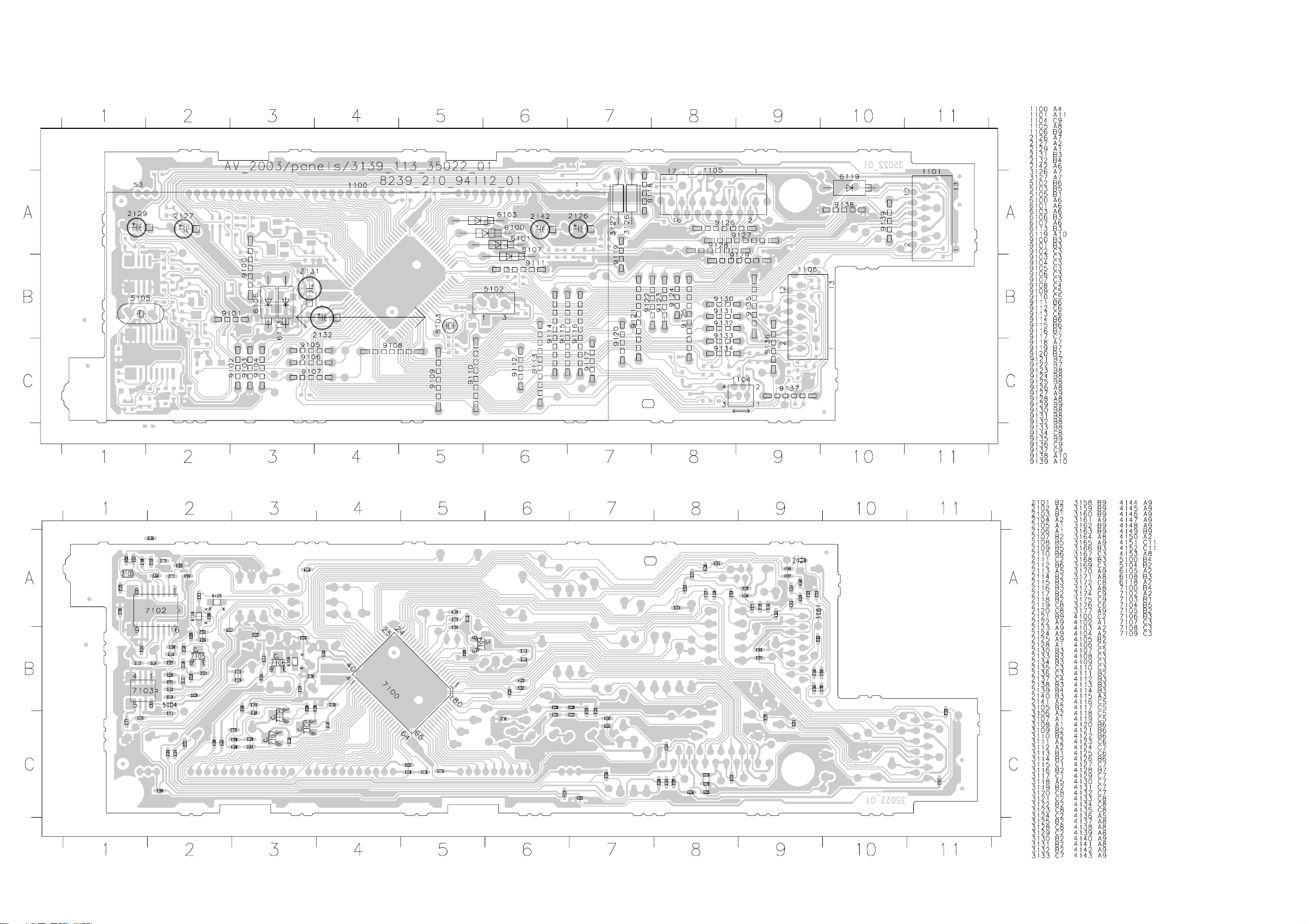
FRONT DISPLAY PART - COMPONENT & CHIPS LAYOUT
This assembly drawing shows a summary of all possible version. For components used in a specific version see schematic and respective parts list.
This assembly drawing shows a summary of all possible version. For components used in a specific version see schematic and respective parts list.
8239 210 94112 .. 3139 113 3502p2 dd wk0250
8239 210 94112 .. 3139 113 3502p2 dd wk0250

6-3a
FRONT DISPLAY PART - COMPONENT & CHIPS LAYOUT (pt 4 board)
This assembly drawing shows a summary of all possible version. For components used in a specific version see schematic and respective parts list.
6-3a
This assembly drawing shows a summary of all possible version. For components used in a specific version see schematic and respective parts list.
PART A
8239 210 94114 .. 3139 113 3502p4 dd wk0405
PART B
8239 210 94114 .. 3139 113 3502p4 dd wk0405
6-3b
e
FRONT DISPLAY PART - CHIPS LAYOUT (pt 4 board) PART A
This assembly drawing shows a summary of all possible version. For components used in a sp
6-3b
PART A

6-3c
FRONT DISPLAY PART - CHIPS LAYOUT (pt 4 board) PART B
in a specific version see schematic and respective parts list.
6-3c
PART B
8239 210 94114 .. 3139 113 3502p4 dd wk0405
6-4
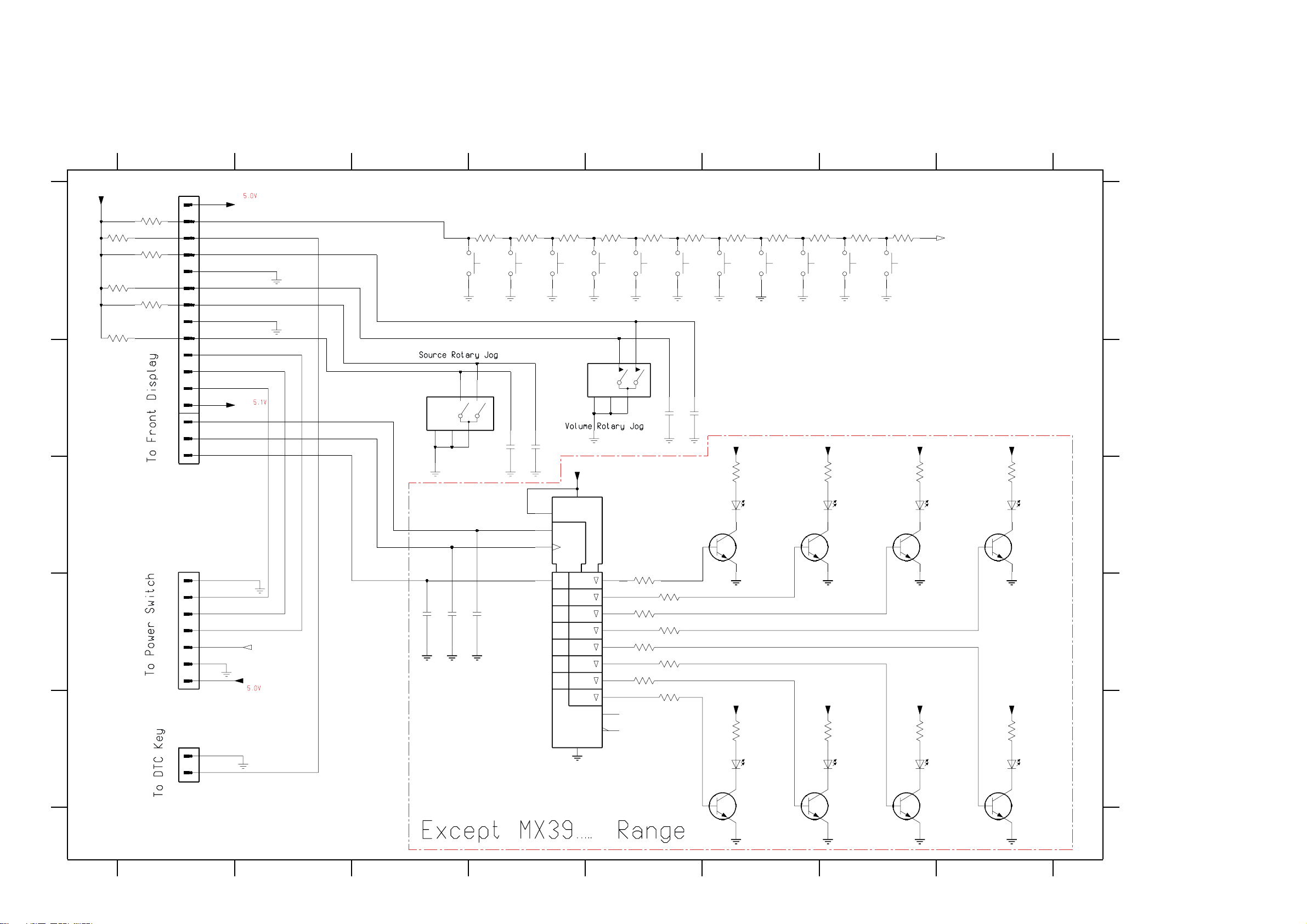
FRONT CONTROL PART - CIRCUIT DIAGRAM
6-4
A
B
1300 A1
1301 A3
1302 A4
1303 A4
+C
1304 A4
1305 A5
1306 A5
1307 A6
3331
2K7
3333
10K
3335
10K
1308 A6
1309 A6
1310 A7
1311 A7
1313 C1
1314 B4
1315 B3
1316 E1
2304 B5
2305 B5
2306 B4
2307 B4
2308 D3
2309 D3
2310 D4
3303 A4
3304 A4
3305 A4
3306 A5
3307 A5
3308 A5
3309 A6
3310 A6
3311 A6
3312 A7
3330 A1
3331 A1
3332 A1
3333 A1
3334 A1
3335 A1
3336 A7
3337 D5
3338 D5
3339 D5
3340 D5
3341 D5
3342 D5
3343 D5
3344 E5
3345 C6
3346 C7
3347 C7
3348 C8
3349 E6
3350 E7
3351 E7
3352 E8
6300 C6
6301 C7
6302 C8
6303 C8
6304 E6
6305 E7
6306 E8
6307 E8
7300 C5
7301 C6
7302 C7
7303 C7
7304 C8
7305 E6
7306 E7
7307 E7
7308 E8
12345678
1300
3330
2K7
3332
10K
3334
10K
1
2
3
4
5
6
7
8
9
11
12
13
10
14
15
16
+C
Key1
Key0
Rot_Vol_B
Rot_Vol_A
Rot_Jog_B
Rot_Jog_A
LPS_LED
RC6
Stdby_LED
+D
LedShStr
LedShClk
LedShData
GND_B
EVE
1315
SWEETSPOT
4
5
1301
GND_B
1
A3B
C
2
3303
150R
PLAY
1302
GND_B
2306
3304
220R
10n
STOP
1303
GND_B
10n
2307
3305
270R
1314
PREVIOUS
3306
390R 1K8
1304
GND_B
EVE
GND_B
13
MT14MT2
5
NEXT
1305
2
3307
560R
SURROUND
3308
820R
1306
GND_B
10n
2304
2305
CLK
1307
GND_B
10n
3309
1K2
TUNING
1308
GND_B
3310
PROGRAM
1309
GND_B
TREBLE
3311
2K7
1310
GND_B
3312
4K7
BASS
1311
GND_B
3336
10K
Stdby_Key
+D +D +D +D
A
B
C
D
E
FE-ST-VK-N
1313
FE-ST-VK-N
1316
EH-S
1
2
3
4
5
6
7
1
2
Stdby_LED
RC6
LPS_LED
GND_B
Key0
Stdby_Key
+C
GND_B
2308
47p
2309
47p
2310
47p
SRG8
15
EN1
1
STB
3
2
D1
+D
16
8
7300
74HC4094D
3337
4
120R
5
3339
6
120R
7
3341
14
120R
13
3343
12
120R
11
9
10
3338
120R
3340
120R
3342
120R
3344
120R
3345
120R
LTL-816TDK3
7301
BC847B
6300
3346
120R
LTL-816TDK3
7302
BC847B
6301
3347
120R
6302
LTL-816TDK3
7303
BC847B
3348
+D +D +D +D
3349
120R
LTL-816TDK3
7305
BC847B
6304
3350
120R
LTL-816TDK3
7306
BC847B
6305
3351
120R
6306
LTL-816TDK3
7307
BC847B
3352
120R
6303
LTL-816TDK3
7304
BC847B
120R
6307
LTL-816TDK3
7308
BC847B
C
D
E
12345678
6-4a
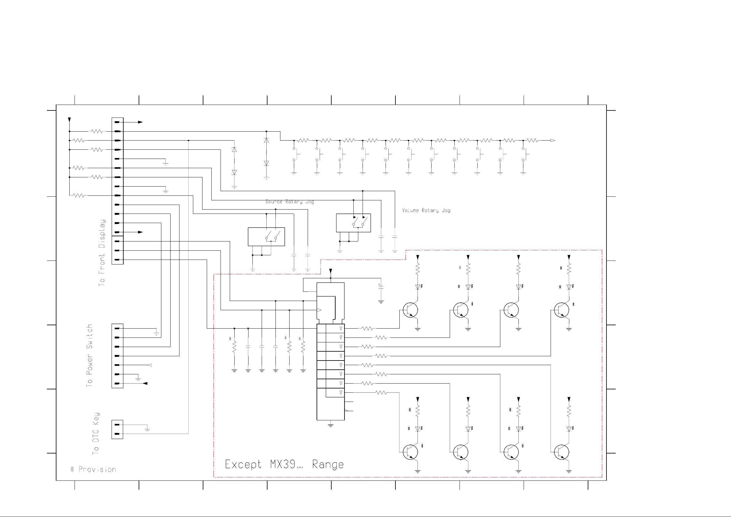
FRONT CONTROL PART - CIRCUIT DIAGRAM (For pt 4 board)
6-4a
A
B
C
D
E
1300 A1
1301 A4
1302 A4
1303 A5
+C
1304 A5
1305 A5
1306 A6
1307 A6
3331
2K7
3333
10K
3335
10K
1308 A6
1309 A7
1310 A7
1311 A7
1313 C1
1314 B4
1315 B3
1316 E1
2300 C5
2304 B5
2305 B5
2306 B4
2307 B4
2308 D3
2309 D3
2310 D4
3303 A4
3304 A4
3305 A5
3306 A5
3307 A5
3308 A6
3309 A6
3310 A7
3311 A7
3312 A7
3330 A1
3331 A1
3332 A1
3333 A1
3334 A1
3335 A1
3336 A8
3337 D5
3338 D5
3339 D5
3340 D5
3341 D5
3342 D5
3343 D5
3344 E5
3345 C6
3346 C7
3347 C7
3348 C8
3349 E6
3350 E7
3351 E7
3352 E8
3353 D3
3354 D4
3355 D4
6300 C6
6301 C7
6302 C7
6303 C8
6304 E6
6305 E7
6306 E7
6307 E8
6308 A4
6309 A4
6310 A3
6311 A3
7300 C5
7301 C6
7302 C7
7303 C7
7304 C8
7305 E6
7306 E7
7307 E7
7308 E8
12345678
1300
3330
2K7
3332
10K
3334
10K
FE-ST-VK-N
1313
FE-ST-VK-N
1316
EH-S
1
2
3
4
5
6
7
8
9
10
11
12
13
14
15
16
1
2
3
4
5
6
7
1
2
+C
Key1
Key0
Rot_Vol_B
Rot_Vol_A
Rot_Jog_B
Rot_Jog_A
LPS_LED
RC6
Stdby_LED
+D
LedShStr
LedShClk
LedShData
Stdby_LED
RC6
LPS_LED
GND_B
Key0
Stdby_Key
+C
GND_B
GND_B
6310
BZX384-C6V8
6311
GND_B
BZX384-C6V8
EVE
1315
10K
2308
3353
BZX384-C6V8
GND_B
4
5
47p
2309
6308
BZX384-C6V8
6309
1
A3B
C
2
47p
47p
2310
SWEETSPOT
3303
150R
1301
GND_B
10n
2306
10K
3355
3354
PLAY
3304
220R
1302
GND_B
10n
2307
15
EN1
1
STB
3
2
D1
10K
STOP
1303
GND_B
EVE 1 3
1314
MT1
+D
16
SRG8
8
PREVIOUS
3305
270R
GND_B
MT2
4
5
7300
74HC4094D
4
5
6
7
14
13
12
11
9
10
1304
2
3337
120R
3339
120R
3341
120R
3343
120R
390R
NEXT
1305
GND_B
10n
2304
2300
3338
120R
3340
120R
3342
120R
3344
120R
3307
560R
16V10u
SURROUND
GND_B
10n
2305
3312
4K7
BASS
1311
GND_B
3336
10K
Stdby_Key
1306
3308
820R
CLK
1307
GND_B
3309
1K2
TUNING
1308
GND_B
33103306
1K8
PROGRAM
1309
GND_B
TREBLE
3311
2K7
1310
GND_B
+D +D +D +D
3345
6300
120R
LTL-816TDK3
7301
BC847B
3346
6301
120R
LTL-816TDK3
7302
BC847B
3347
6302
120R
LTL-816TDK3
7303
BC847B
+D +D +D +D
3349
6304
120R
LTL-816TDK3
7305
BC847B
3350
6305
120R
LTL-816TDK3
7306
BC847B
3351
6306
120R
LTL-816TDK3
7307
BC847B
3348
6303
3352
6307
120R
LTL-816TDK3
7304
BC847B
120R
LTL-816TDK3
7308
BC847B
A
B
C
D
E
12345678
6-5
FRONT CONTROL PART - COMPONENT & CHIPS LAYOUT
This assembly drawing shows a summary of all possible version. For components used in a specific version see schematic and respective parts list.
6-5
8239 210 94122 .. 3139 113 3502p2 dd wk0250
This assembly drawing shows a summary of all possible version. For components used in a specific version see schematic and respective parts list.
8239 210 94122 .. 3139 113 3502p2 dd wk0250

6-5a
FRONT CONTROL PART - COMPONENT LAYOUT (For pt 4 board)
This assembly drawing shows a summary of all possible version. For components used in a specific version see schematic and respective parts list.
6-5a
8239 210 94124 .. 3139 113 3502p4 dd wk0405

6-5b
FRONT CONTROL PART - CHIPS LAYOUT (For pt 4 board)
This assembly drawing shows a summary of all possible version. For components used in a specific version see schematic and respective parts list.
6-5b
8239 210 94124 .. 3139 113 3502p4 dd wk0405
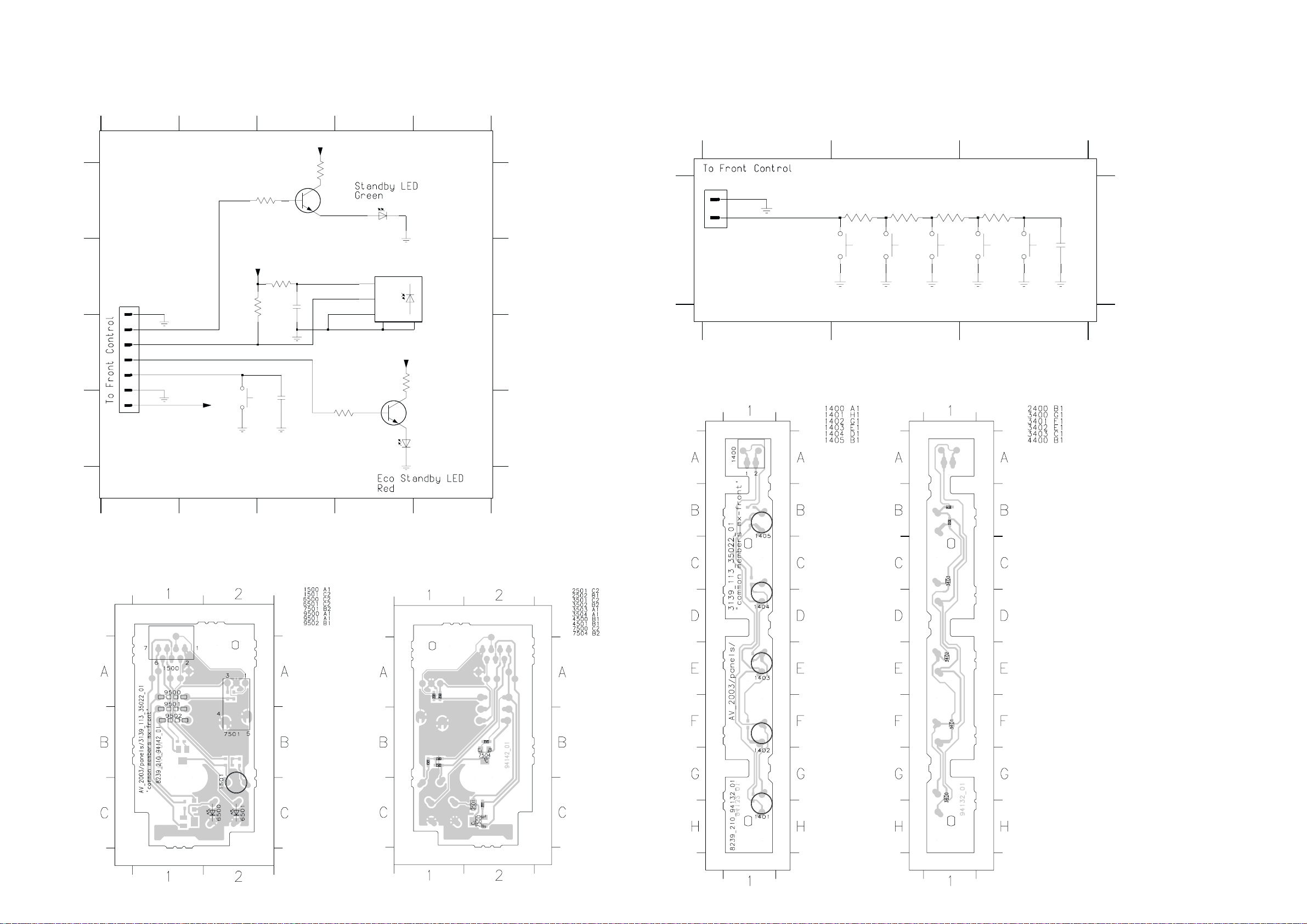
6-6
POWER SWITCH PART - CIRCUIT DIAGRAM DTC KEY PART - CIRCUIT DIAGRAM
6-6
A
B
C
D
12345
+C
3502
120R
1500
1
2
FE-ST-VK-N
3505
470R
+C
3503
100R
10K
3504
Stdby_LED
3
RC6
4
LPS_LED
5
Stdby_key
6
GND_B
7
+C
1501
GND_B
Standby
2502
GND_B
2u2
100p
2501
7504
BC847B
3506
470R
LTL-816GE
3
1
2
GND
6501
7501
VS
OUT
GND
5
TSOP4836ZC1
4
+C
3501
470R
7500
BC847B
6500
LTL-816EELC
A
B
C
D
1500 B1
1501 D2
2501 B3
2502 D3
3501 C4
3502 A3
3503 B3
3504 B3
3505 A3
3506 D4
6500 D4
6501 A4
7500 D4
7501 B5
7504 A3
T500 B1
T501 C1
T502 C1
T503 C1
T504 C1
T505 D1
1400 A1
1401 A1
1402 A2
1403 A2
1404 A3
1405 A3
2400 A3
3400 A2
3401 A2
3402 A2
3403 A3
123
1400
1
2
AA
EH-S
GND_B
DISC1
1401
GND_B
3400
150R
DISC2
1402
GND_B
3401
220R
DISC3
1403
3402
270R
DISC4
1404
3403
390R
DISC5
1405
GND_BGND_BGND_B
GND_B
8239 210 94132 dd wk0250
2400
100p
123
DTC KEY PART - COMPONENT & CHIP LAYOUTS
8239 210 94142 dd wk0250
12345
POWER SWITCH PART - COMPONENT & CHIP LAYOUTS
8239 210 94142 .. 3139 113 3502p2 dd wk0250
8239 210 94142 .. 3139 113 3502p2 dd wk0250
8239 210 94132 .. 3139 113 3502p2 dd wk0250
8239 210 94132 .. 3139 113 3502p2 dd wk0250
This assembly drawing shows a summary of all possible version. For components used in
a specific version see schematic and respective parts list.
This assembly drawing shows a summary of all possible version. For components used in
a specific version see schematic and respective parts list.
This assembly drawing shows a summary of all possible version. For components used in a specific version see schematic and respective parts list.
This assembly drawing shows a summary of all possible version. For components used in a specific version see schematic and respective parts list.
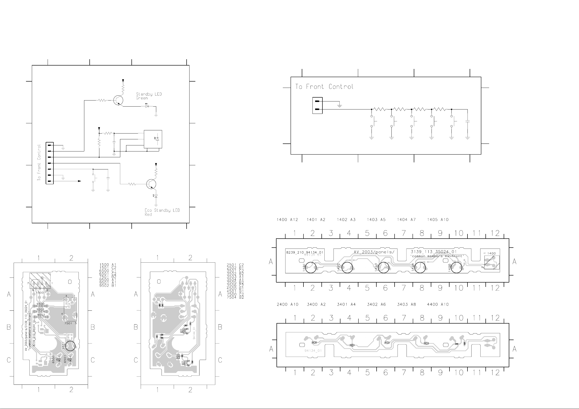
6-6a
6-6a
POWER SWITCH PART - CIRCUIT DIAGRAM (For pt 4 board) DTC KEY PART - CIRCUIT DIAGRAM (For pt 4 board)
A
B
C
1500 B1
1501 C1
2501 B2
2502 C2
1500
1
2
FE-ST-VK-N
3501 C3
3502 A2
3503 B2
3504 B2
3505 A2
3506 C3
6500 C3
6501 A3
7500 C3
7501 B3
7504 A2
12 3
+C
3502
120R
3505
470R
+C
3503
100R
10K
3504
Stdby_LED
3
RC6
4
LPS_LED
5
Stdby_key
6
GND_B
7
+C
1501
GND_B
Standby
2502
GND_B
2u2
100p
2501
7504
BC847B
3506
470R
LTL-816GE
3
1
2
GND
6501
TSOP4836ZC1 7501
VS
OUT
GND
5
3501
7500
BC847B
6500
4
+C
470R
LTL-816EELC
A
B
C
1400 A1
1401 A2
1402 A2
1403 A2
1404 A3
1405 A3
2400 A3
3400 A2
3401 A2
3402 A3
3403 A3
123
1400
1
GND_B
2
AA
EH-S
DISC1
1401
GND_B
3400
150R
DISC2
1402
GND_B
DISC3
3401
220R
1403
DISC4
3402
270R
1404
GND_BGND_B
3403
390R
DISC5
1405
GND_B
GND_B
8239 210 94134 ..3502p4 dd wk0405
2400
100p
123
DTC KEY PART - COMPONENT & CHIP LAYOUTS (pt 4 board)
8239 210 94144 ..3502p4 dd wk0405
12 3
POWER SWITCH PART - COMPONENT & CHIP LAYOUTS (pt 4 board)
This assemby drawing shows a summary of all possible versions. For
components used in a specific version see schematic and respective parts list.
This assemby drawing shows a summary of all possible versions. For
components used in a specific version see schematic and respective parts list.
This assemby drawing shows a summary of all possible versions. For components used in a specific version see schematic and respective parts list.
8239 210 94134 ... 3502p4 dd wk0405
This assemby drawing shows a summary of all possible versions. For components used in a specific version see schematic and respective parts list.
8239 210 94144 ..3502p4 dd wk0405
8239 210 94134 ... 3502p4 dd wk0405
8239 210 94144 ..3502p4 dd wk0405
 Loading...