

Philips MPSH10 Datasheet
DISCRETE SEMICONDUCTORS
DATA SH EET
ook, halfpage
M3D186
MPSH10
NPN 1 GHz general purpose
switching transistor
Product specification
Supersedes data of September 1995
1998 Aug 27
File under Discrete Semiconductors, SC14
Philips Semiconductors Product specification
NPN 1 GHz general purpose switching transistor MPSH10
FEA TURES
• Low cost
• High power gain.
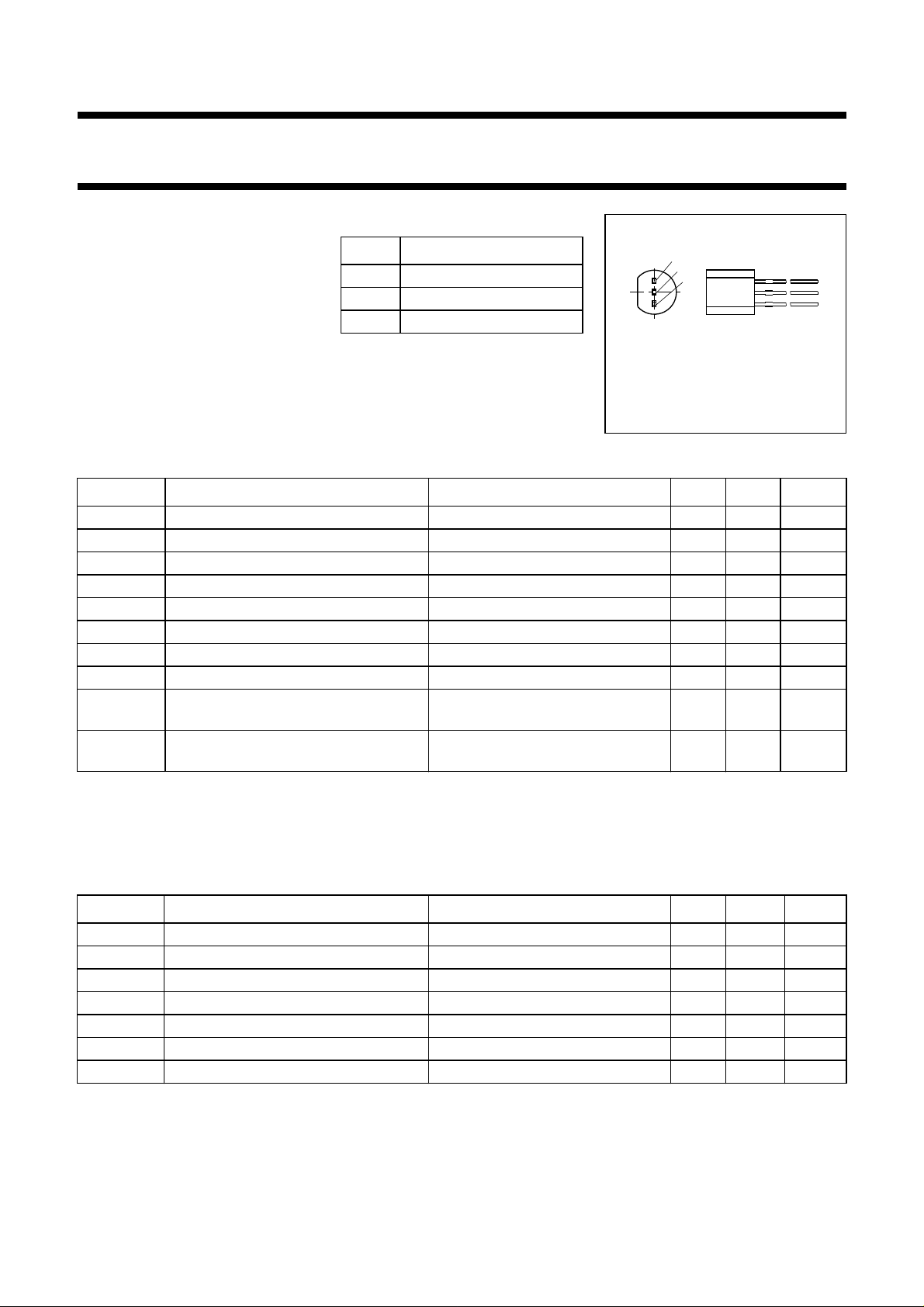
PINNING
PIN DESCRIPTION
1 collector
age
1
2
3
2 emitter
DESCRIPTION
3 base
MSB033
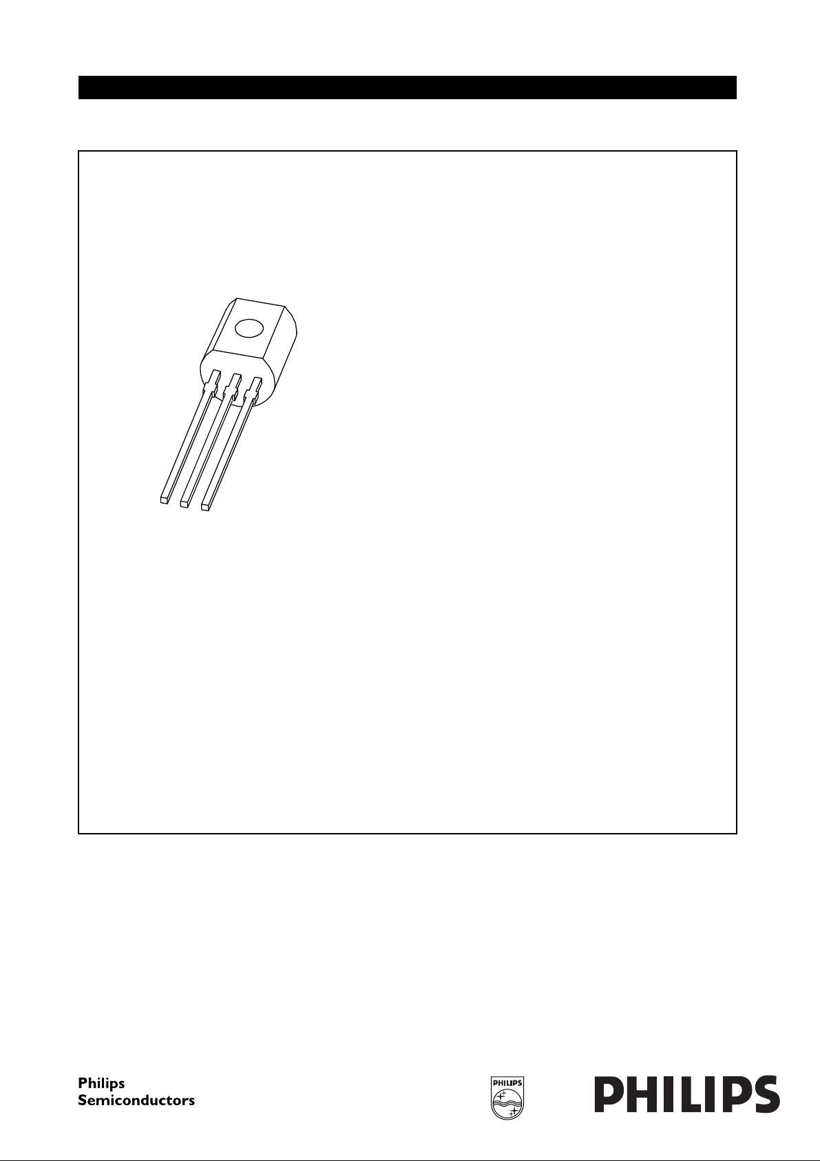
Silicon NPN general purpose
transistor in a SOT54 (TO-92)
package. PNP complement is the
MPSH81.
Marking code: PSH10.
Fig.1 SOT54.
QUICK REFERENCE DATA
SYMBOL PARAMETER CONDITIONS MIN. MAX. UNIT
V
CBO
V
CEO
V
EBO
P
tot
T
j
h
FE
C
re
C
rb
f
T
r
bCc
collector-base voltage open emitter − 30 V
collector-emitter voltage open base − 25 V
emitter-base voltage open collector − 3V
total power dissipation Ts=25°C; note 1 − 1W
junction temperature − 150 °C
DC current gain VCE=10V; IC=4mA 60 −
collector-emitter feedback capacitance VCB=10V; IE= 0; f = 1 MHz − 0.7 pF
collector-base feedback capacitance VCB=10V; IE= 0; f = 1 MHz 0.35 0.65 pF
transition frequency VCE=10V; IC= 4 mA;
f = 100 MHz; T
amb
=25°C
collector-base time constant VCE=10V; IC= 4 mA;
f = 100 MHz; T
amb
=25°C
650 − MHz
− 9ps
Note
is the temperature at the soldering point of the collector lead, 4 mm from the body.
1. T
s
LIMITING VALUES
In accordance with the Absolute Maximum Rating System (IEC 134).
SYMBOL PARAMETER CONDITIONS MIN. MAX. UNIT
V
CBO
V
CEO
V
EBO
I
C
P
tot
T
stg
T
j
collector-base voltage open emitter − 30 V
collector-emitter voltage open base − 25 V
emitter-base voltage open collector − 3V
collector current (DC) − 40 mA
total power dissipation Ts=25°C; note 1 − 1W
storage temperature −65 +150 °C
junction temperature − 150 °C
Note
1. Tsis the temperature at the soldering point of the collector lead, 4 mm from the body.
1998 Aug 27 2
Philips Semiconductors Product specification
NPN 1 GHz general purpose switching transistor MPSH10
THERMAL CHARACTERISTICS
SYMBOL PARAMETER CONDITIONS VALUE UNIT
R
th j-s
R
th j-a
Note
1. Ts is the temperature at the soldering point of the collector lead, 4 mm from the body.
CHARACTERISTICS
=25°C unless otherwise specified.
T
j
SYMBOL PARAMETER CONDITIONS MIN. MAX. UNIT
V
(BR)CBO
V
(BR)CEO
V
(BR)EBO
V
CEsat
V
BEon
I
CBO
I
EBO
h
FE
C
re
C
rb
f
T
r
bCc
thermal resistance from junction to soldering point note 1 125 K/W
thermal resistance from junction to ambient 250 K/W
collector-base breakdown voltage open emitter; IC= 100 µA; IE=0 30 − V
collector-emitter breakdown voltage open base; IC= 1 mA; IB=0 25 − V
emitter-base breakdown voltage open collector; IE=10µA; IC=0 3 − V
collector-emitter saturation voltage IC= 4 mA; IB= 0.4 mA − 0.5 V
base-emitter ON voltage VCE= 10 V; IC=4mA − 0.95 V
collector-base cut-off current VCB= 25 V; IE=0 − 100 nA
emitter-base cut-off current VCB= 25 V; IC=0 − 100 nA
DC current gain VCE= 10 V; IC=4mA 60 −
collector-emitter feedback capacitance VCB= 10 V; IE=ie= 0; f = 1 MHz − 0.7 pF
collector-base feedback capacitance VCB= 10 V; IC=ic= 0; f = 1 MHz 0.35 0.65 pF
transition frequency VCE= 10 V; IC= 4 mA;
f = 100 MHz; T
amb
=25°C
collector-base time constant VCB= 10 V; IC= 4 mA;
f = 100 MHz; T
amb
=25°C
650 − MHz
− 9ps
1998 Aug 27 3
 Loading...