

Philips MPSA26 Datasheet
DISCRETE SEMICONDUCTORS
DATA SH EET
ook, halfpage
M3D186
MPSA26; MPSA27
NPN Darlington transistors
Product specification
Supersedes data of 1997 Apr 17
1999 Apr 27
Philips Semiconductors Product specification
NPN Darlington transistors MPSA26; MPSA27
FEATURES
• High current (max. 500 mA)
• Low voltage (max. 60 V)
• High DC current gain (min. 10000).
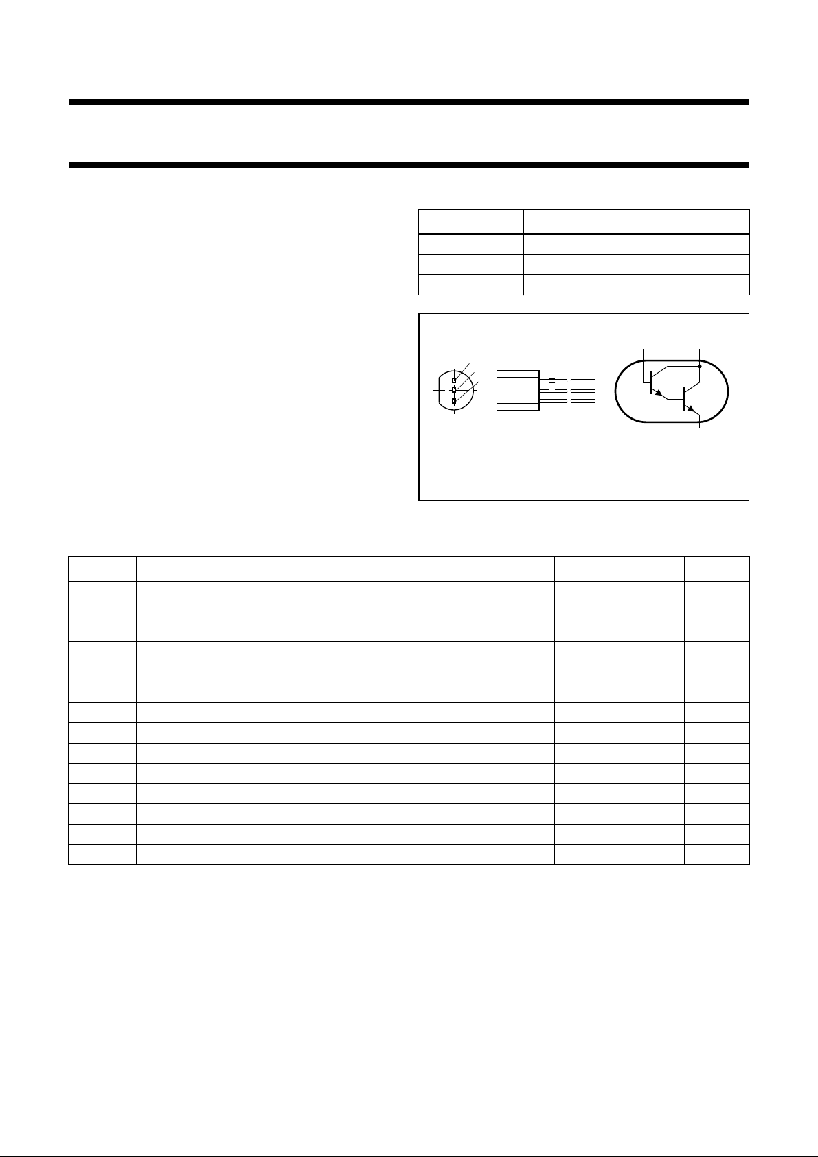
PINNING
PIN DESCRIPTION
1 collector
2 base
3 emitter
APPLICATIONS
• High gain amplification.
DESCRIPTION
NPN Darlington transistor in a TO-92; SOT54 plastic
package.
handbook, halfpage
1
2
3
2
MAM252
1
TR1
TR2
3
Fig.1 Simplified outline (TO-92; SOT54)
and symbol.
LIMITING VALUES
In accordance with the Absolute Maximum Rating System (IEC 134).
SYMBOL PARAMETER CONDITIONS MIN. MAX. UNIT
V
CBO
collector-base voltage open emitter
MPSA26 − 50 V
MPSA27 − 60 V
V
CES
collector-emitter voltage VBE=0
MPSA26 − 50 V
MPSA27 − 60 V
V
EBO
I
C
I
CM
I
B
P
tot
T
stg
T
j
T
amb
emitter-base voltage open collector − 10 V
collector current (DC) − 500 mA
peak collector current − 1A
base current (DC) − 100 mA
total power dissipation T
≤ 25 °C; note 1 − 500 mW
amb
storage temperature −65 +150 °C
junction temperature − 150 °C
operating ambient temperature −65 +150 °C
Note
1. Transistor mounted on an FR4 printed-circuit board.
1999 Apr 27 2
Philips Semiconductors Product specification
NPN Darlington transistors MPSA26; MPSA27
THERMAL CHARACTERISTICS
SYMBOL PARAMETER CONDITIONS VALUE UNIT
R
th j-a
Note
1. Transistor mounted on an FR4 printed-circuit board.
CHARACTERISTICS
=25°C unless otherwise specified.
T
j
SYMBOL PARAMETER CONDITIONS MIN. TYP. MAX. UNIT
I
CBO
I
CBO
I
EBO
h
FE
V
CEsat
V
BEsat
V
BEon
f
T
thermal resistance from junction to ambient note 1 250 K/W
collector cut-off current IE= 0; VCB=40V
MPSA26 −−100 nA
collector cut-off current IE= 0; VCB=50V
MPSA27 −−100 nA
emitter cut-off current IC= 0; VEB=10V −−100 nA
DC current gain IC= 10 mA; VCE= 5 V; see Fig.2 10000 −−
I
= 100 mA; VCE= 5 V; see Fig.2 10000 −−
C
collector-emitter saturation voltage IC= 100 mA; IB= 0.1 mA −−1.5 V
base-emitter saturation voltage IC= 100 mA; IB= 0.1 mA −−1.5 V
base-emitter on-state voltage IC= 100 mA; VCE=5V −−2V
transition frequency IC= 30 mA; VCE= 5 V; f = 100 MHz 125 220 − MHz
1999 Apr 27 3
 Loading...