

Page 1

Colour Television Chassis
MP1.1U
AA
Contents Page
1 Specification 2
2 Precautions and Notices 13
3 Operation 14
4 Trouble shooting chart 20
5 White-Balance Adjustment 25
6 DDC program and test 26
7 Flash Update 28
8 Software Platform Reference TV Application 31
9 Block diagram & Explain 33
10 Waveform of Signal 37
11 Check and Measure 44
12 Mechanical of Cabinet 47
13 PCB Layout 62
14 Circuit Diagrams 65
15 Spare Parts List 32MF130A/37 88
16 Spare Parts List 32MF230A/37 88
17 Revision List 89
©
Copyright 2005 Philips Consumer Electronics B.V. Eindhoven, The Netherlands.
All rights reserved. No part of this publication may be reproduced, stored in a
retrieval system or transmitted, in any form or by any means, electronic,
mechanical, photocopying, or otherwise without the prior permission of Philips.
Published by JH 567 TV Service Printed in the Netherlands Subject to modification EN 3122 785 15691
Page 2

1、 SPECIFICATION 42MF130A/37
1-1 General Specification
NOTE:
*This model complies with the specifications listed below.
*Designs and specifications are subject to change without notice.
*This model may not be compatible with features and/or specifications that may be added in the future.
Item Specification
Screen size 107cm(42 inch) plasma display panel
Panel Spec
Component
INPUT
DVI INPUT
VGA INPUT
Video INPUT
Video Output
Aspect
Display pixels 852(H) x 480 (V)
V iewing Angle 160°
Number of color 1670 million colors
Contrast Ration 3000:1 (in dark room)
Peak brightness(with filter) 400 cd/m
Y 1V(p-p), 75 ohm
Rear(2 Group)
Pr/Cr 0.7 V (p-p), 75 ohm
Pb/Cb 0.7 V (p-p), 75 ohm
AUDIO 150 mV (rms)
Rear(1 Group) DVI-D
Rear(1 Group) D-SUB 15Pin
S-Video
Side(1 Group)
Rear(1 Group)
Video
Audio
Rear(1 Group)
VIDEO
AUDIO
16:9
2
Suggested resolutions:
1080i, 480p, 480i, 720p
HDCP compliant
E-EDID compliant
Suggested scan rates:
1080i/60Hz, 1080p/60Hz, 720p/60Hz
E-EDID compliant
Suggested scan rates:
x 480/60Hz, 800 x 600/60Hz, 1024 x 768/60Hz
640
Y : 1 V(p-p), 75 ohm, negative sync.
C : 0.286 V(p-p) (burst signal), 75 ohm
1 V(p-p), 75 ohm, negative sync.
150 mV(rms)
1 V(p-p), 75 ohm, negative sync
150 mV(rms)
Channel Coverage:
VHF: 2 through 13
Television
System
NTSC standard
ATSC standard (8VSB)
UHF: 14 through 69
Cable TV: Mid band (A-8 through A-1, A through I)
Super band (J through W)
Hyper band (AA through ZZ, AAA, BBB)
Ultra band (65 through 94, 100 through 125)
Audio Power
Internal Speaker 5 W + 5 W
Power input sources 100 -240V, 50/60 Hz
Power
Dimension
Power consumption
Width x Height x Depth
350 W (on average) / 1W in standby mode
(power cord plugged in and power OFF)
Without Stand: 1038 x 660 x 82 (mm)
Include Stand: 1038 x 726.5 x 270 (mm)
Without Stand 35.5 kg
Net weight
With Stand 43 kg
Accessory
Choose Part
1pcs power cord, 1pcs remote control, (with two *AAA*sized alkaline batteries)
Wall Mounting Bracket
NOTE: This TV does not provide ATSC TV/S-VIDEO/HD/VGA/DVI Output.
2
Page 3
1、 SPECIFICATION 42MF230A/37
1-1 General Specification
NOTE:
*This model complies with the specifications listed below.
*Designs and specifications are subject to change without notice.
*This model may not be compatible with features and/or specifications that may be added in the future.
Item Specification
Screen size 107cm(42 inch) plasma display panel
Panel Spec
Component
INPUT
DVI INPUT
VGA INPUT
Video INPUT
Video Output
Aspect
Display pixels 1024(H) x 768 (V)
V iewing Angle 160°
Number of color 1670 million colors
Contrast Ration 3000:1 (in dark room)
Max. brightness 1000 cd/m
Y 1V(p-p), 75 ohm
Rear(2 Group)
Pr/Cr 0.7 V (p-p), 75 ohm
Pb/Cb 0.7 V (p-p), 75 ohm
AUDIO 150 mV (rms)
Rear(1 Group) DVI-D
Rear(1 Group) D-SUB 15Pin
S-Video
Side(1 Group)
Rear(1 Group)
Video
Audio
Rear(1 Group)
VIDEO
AUDIO
16:9
2
Suggested resolutions:
1080i, 480p, 480i, 720p
HDCP compliant
E-EDID compliant
Suggested scan rates:
1080i/60Hz, 480p/60Hz, 720p/60Hz
E-EDID compliant
Suggested scan rates:
x 480/60Hz, 800 x 600/60Hz, 1024 x 768/60Hz
640
Y : 1 V(p-p), 75 ohm, negative sync.
C : 0.286 V(p-p) (burst signal), 75 ohm
1 V(p-p), 75 ohm, negative sync.
150 mV(rms)
1 V(p-p), 75 ohm, negative sync
150 mV(rms)
Channel Coverage:
VHF: 2 through 13
Television
System
NTSC standard
ATSC standard (8VSB)
UHF: 14 through 69
Cable TV: Mid band (A-8 through A-1, A through I)
Super band (J through W)
Hyper band (AA through ZZ, AAA, BBB)
Ultra band (65 through 94, 100 through 125)
Audio Power
Internal Speaker 5 W + 5 W
Power input sources 100 -240V, 50/60 Hz
Power
Dimension
Power consumption
Width x Height x Depth
450 W (on average) / 1W in standby mode
(power cord plugged in and power OFF)
Without Stand: 1038 x 660 x 82 (mm)
Include Stand: 1038 x 726.5 x 270 (mm)
Without Stand 35.5 kg
Net weight
With Stand 43 kg
Accessory
Choose Part
1pcs power cord, 1pcs remote control, (with two *AAA*sized alkaline batteries)
Wall Mounting Bracket
NOTE: This TV does not provide ATSC TV/S-VIDEO/HD/VGA/DVI Output.
3
Page 4

1-2 Feature Summary 42MF130A/37
The following is the specification summary for the display:
107 cm (42”) 16:9 PLASMA DISPLAY PANEL
Resolutions: 852 (H) X 480 (V) pixels, (1 pixel = 1 R, G, B cells)
1.095 mm (H) X 1.110mm(V) pixel pitch.
Viewing Angle: 160° Vertically and Horizontally
Typical Maximum Contrast Ratio: 3000:1
Typical Maximum Brightness (with filter): 400 cd/m
2
ATSC receiver, MPEG-2 decoder
NTSC receiver, Video decoder
Closed Caption / V-chip
Composite, S-Video, and component video receiver
DVI digital video interface
D-SUB analog video with rate 50Hz to 85 Hz vertical refresh rate and 31KHz to
80KHz horizontal frequency
MIPS controller
Field upgradeable firmware
Universal Power Supply designed for worldwide application
Operating power consumption less than 350 W
Standby power consumption less than 1 W
UL, FCC, certification
Dimension: width – 1038mm, height – 660mm, depth – 82mm, weight – 35 Kg
4
Page 5

1-2 Feature Summary 42MF230A/37
The following is the specification summary for the display:
z 107 cm (42”) 16:9 PLASMA DISPLAY PANEL
z Resolutions: 1024 (H) X 768(V) pixels, (1 pixel = 1 R, G, B cells)
z 0.912 mm (H) X 0.693mm(V) pixel pitch.
z Viewing Angle: 160° Vertically and Horizontally
z Typical Maximum Contrast Ratio: 3000:1
z Typical Maximum Brightness: 1000 cd/m2
z ATSC receiver, MPEG-2 decoder
z NTSC receiver, Video decoder
z Closed Caption / V-chip
z Composite, S-Video, and component video receiver
z DVI digital video interface
z D-SUB analog video with rate 50Hz to 85 Hz vertical refresh rate and 31KHz to
80KHz horizontal frequency
z MIPS controller
z Field upgradable firmware
z Universal Power Supply designed for worldwide application
z Operating power consumption less than 450 W
z Standby power consumption less than 1 W
z UL, FCC, certification
z Main Dimension: width 1038mm, height 640mm, depth 110mm, weight 43 Kg
5
Page 6
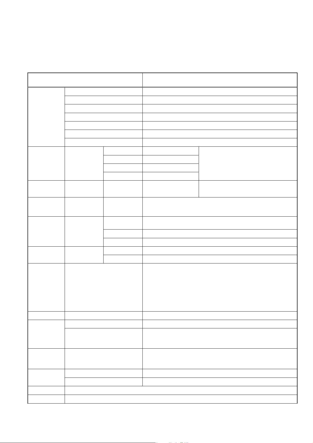
1-3 External interface
Most of these interfaces are located at the back-panel. There’s also a group of connectors located
on the side of this device for easier access. The following figures depict these A/V connectors.
Side A/V Connectors
S-Video Video L R Earphone
AV2 Input
RS-232
ANT
ATSC/NTSC
1-3-1 Video/Audio Inputs
The following sections specify the video/audio inputs for 42MFx30A/37
1-3-1-1 TV A ntenna Interface
①. TV Antenna Connector
42MFx30A/37 shall provide a F-type cable connector with 75 ohms termination on its back
panel for reception of radio frequency signals.
②. TV Systems
42MFx30A/37 shall be capable of receiving the following broadcasting systems in the North
America region.
• Analog terrestrial and cable broadcasting in NTSC system and “M” sound system.
DVI L/ R
DVI Input
Back Panel A/V Connectors
AV3 Component Input
Y Pb/Cb Pr/Cr R L
VGA L/ R
PC Input
Y Pb/Cb Pr/Cr R L
AV4 Component Input
AV Output
Video R L
S-Video Video R L
AV1 I np u t
• All 18 formats specified for ATSC digital broadcasting
• Clear QAM digital cable broadcasting
③. TV Channel Coverage
The RF tuner shall be capable of covering 55.25 to 859.25 MHz and tuning to the following
6
Page 7

channels:
• VHF: channel 2 through 13
• UHF: channel 14 through 69
• Mid band cable: A1 through A8, A through I
• Super band cable: J through W
• Hyper band cable: AA through ZZ, AAA, BBB
• Ultra band cable: channel 65 through 94, 100 through 125
④. Closed Caption
42MFx30A/37 shall support closed caption and text mode for both video and TV system.
These supports shall include channel ½ and field ½ selectable features.
⑤. V -Chip
42MFx30A/37 shall support MPAA grade for movie and TV Parental Guideline for TV. This
support shall include changeable password.
1-3-1-2 AV1
A standard definition (SD) analog video/audio source designated as AV1 shall be located on its
back panel. It comprises the following electrical connections. Only one of the two video inputs
shall be connected.
①. S-Video Input
42MFx30A/37 shall provide a 4-pin mini-DIN connector for connection to an external
S-Video source.
②. CVBS Video Input
42MFx30A/37 shall provide a RCA type receptacle for connection to an external CVBS
source.
③. Audio Inputs
42MFx30A/37 shall provide two RCA type receptacles for the stereo audio signal associated
with AV1 input.
1-3-1-3 AV2
A standard definition analog video/audio source designated as AV2 shall be located at the side
of 42MFx30A/37. It comprises the following electrical connections. Only one of the two video
inputs shall be connected.
①. S-Video Input
42MFx30A/37 shall provide a 4-pin mini-DIN connector for connection to an external
S-Video source.
②. CVBS Video Input
42MFx30A/37 shall provide a RCA type receptacle for connection to an external CVBS
source.
③. Audio Inputs
42MFx30A/37 shall provide two RCA type receptacles for the stereo audio signal associated
with AV2 input.
1-3-1-4 AV3
A YPbPr/YcbCr type component video interface designated as AV3 shall be located on its back
panel. It comprises the following electrical connections.
①. Video Inputs
42MFx30A/37 shall provide three RCA type receptacles for connection to an external
component video source.
②. Audio Inputs
42MFx30A/37 shall provide two RCA type receptacles for the stereo audio signal associated
7
Page 8

with Component1 input.
1-3-1-5 AV4
A YPbPr/YcbCr type component video interface designated as AV4 shall be located on its back
panel. It comprises the following electrical connections.
①. Video Inputs
42MFx30A/37 shall provide three RCA type receptacles for connection to an external
component video source.
②. Audio Inputs
42MFx30A/37 shall provide two RCA type receptacles for the stereo audio signal associated
with Component2 input.
1-3-1-6 PC Input
42MFx30A/37 accommodates a VGA type computer connection as specified below.
①. Video Input connector
42MF130A/37 shall provide a 15-pin D-Sub connector on its back panel for connection to a
VGA type video source. The VGA signal input on the display shall be capable of receiving
RGB analog video, H and V syncs, and DDC. The table below specifies pin-outs of this
connector.
Analog Connector Pin-outs
PIN
1 RV Red Video
2 GV Green Video
3 BV Blue Video
4 NC None
5 GND Ground (DDC Return)
6 RG Red GND
7 GG Green GND
8 BG Blue GND
9 +5 V +5 V (from the PC)
10 SG Sync Ground
11 NC None
12 SDA DDC Data
13 HS Horizontal Sync
14 VS Vertical Sync
15 SCL DDC Clock
②. Audio Inputs
42MFx30A/37 shall provide a 3.5 mm jack for the stereo audio signal associated with VGA
input.
③. Input Formats
42MFx30A/37 shall support the following input format on its VGA input.
Mode Resolution Total
VGA 640x480@60Hz 800 x 525 31.469 N 59.940 N 25.175
SVGA 800x600@60Hz 1056 x 628 37.879 P 60.317 P 40.000
XGA 1024x768@60Hz 1344x806 48.363 N 60.004 N 65.000
MNEMONIC
SIGNAL
1
6
11 15
Horizontal Vertical
Nominal
Frequency
(KHz)
8
Sync
Polarity
Nominal
Freq.
(Hz)
Sync
Polarity
5
10
Nominal
Pixel
Clock
(MHz)
Page 9
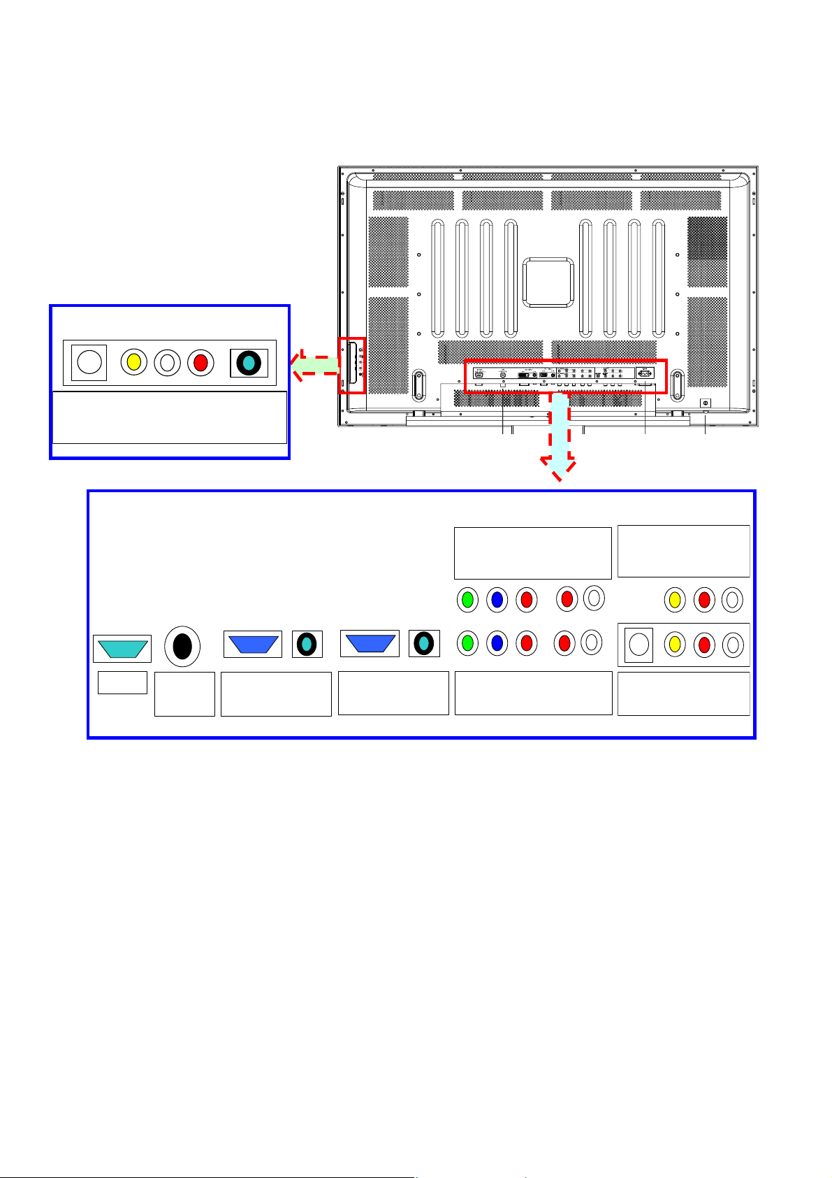
1-3-1-7 DVI
42MFx30A/37 shall accommodate a DVI type digital video source as specified in this section.
①①. Video Inputs
42MFx30A/37 shall provide a 24 contact DVI-D receptacle on its back panel for receiving
TMDS digital video. The table below specifies pin assignments for the DVI-D connector.
DVI-D Digital connector pin assignments
PIN MNEMONIC SIGNAL
1 TX 2 - TMDS Data 2 -
2 TX 2 + TMDS Data 2 +
3 SHLD 2 / 4 TMDS Data 2 / 4 Shield
4 TX 4 - TMDS Data 4 -
5 TX 4 + TMDS Data 4 +
6 DDC Clk DDC Clock
7 DDC Data DDC Data
8 N/C No Connect
9 TX 1 - TMDS Data 1 -
10 TX 1 + TMDS Data 1 +
11 SHLD 1 / 3 TMDS Data 1 / 3 Shield
12 TX 3 - TMDS Data 3 -
13 TX 3 + TMDS Data 3 +
14 +5V +5V Power (from the PC)
15 GND Ground (Return for +5V)
16 HPD Hot Plug Detect
17 TX 0 - TMDS Data 0 -
18 TX 0 + TMDS Data 0 +
19 SHLD 0 / 5 TMDS Data 0 / 5 Shield
20 TX 5 - TMDS Data 5 -
21 TX 5 + TMDS Data 5 +
22 TX CLK SHLD TMDS Clock Shield
23 TX CLK + TMDS Clock +
24 TX CLK - TMDS Clock -
②②. Audio Inputs
42MFx30A/37 shall provide a 3.5 mm jack for the stereo audio signal associated with DVI
.
input
③③. HDCP support
HDCP must be supported on the DVI input. Refer to the High-bandwidth Digital Content
Protection System specification version 1.1 for details.
9
Page 10
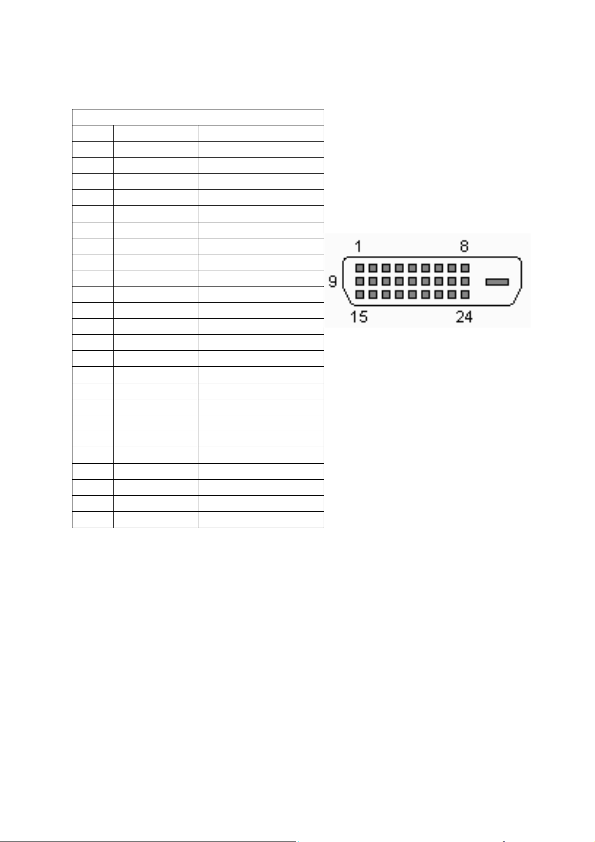
④④. Input Formats
42MF130A/37 shall support the following input format on its DVI input.
minal
No
minal
Mode Resolution Total
VGA 640x480@60Hz 800 x 525 31.469 59.940 25.175
SVGA 800x600@60Hz 1056 x 628 37.879 60.317 40.000
XGA 1024x768@60Hz 1344x806 48.363 60.004 65.000
720P 1280×720P 74.25 60
HFreq
(KHz)
uency
No
Vertical
equency
Fr
(KHz)
minal Pixel
No
ck Frequency
Clo
(MHz)
42MF230A/37 shall support the following input format on its DVI input.
Nominal
Mode Resolution Total
VGA 640x480@60Hz 800 x 525 31.469 59.940 25.175
SVGA 800x600@60Hz 1056 x 628 37.879 60.317 40.000
XGA 1024x768@60Hz 1344x806 48.363 60.004 65.000
720P 1280×720P 45.00 60 74.25
1080i 1920×1080i 33.75 60 74.25
480p 720×480p 31.54 60 27.00
HFrequ
ency
(KHz)
Nominal
Vertical
equency
Fr
(KHz)
Nominal Pixel
ck Frequency
Clo
(MHz)
10
Page 11
1-3-2 Audio/Video Outputs
1-3-2-1 Composite Video Output
42MFx30A/37 shall provide a RCA type receptacle on its back panel for composite video output.
1-3-2-2 Analog Audio Output
42MFx30A/37 shall provide two RCA type receptacles for external connection to a stereo
amplifier.
1-3-2-3 Head Phone
42MFx30A/37 shall provide a 3.5 mm jack at side of 42MFx30A/37 for external connection of a
stereo headphone.
1-3-3 Power Interface
1-3-3-1 Power Connector
42MFx30A/37 shall support an IEC C-13/C-14 (Standard) type male power receptacle for
connection to AC power source.
1-3-3-2 Power Input Range
The operating range shall be from 100 to 265 VAC sinusoidal for 42MF130A and 100 to 240VAC
sinusoidal for 42MF230A. Input power frequency range shall be from 50 to 60 Hz over the
specified input voltage range.
1-3-3-3 Power Consumption
①①. Operating Power
Power consumption for the display over the specified voltage and frequency ranges shall be
les
s than 350 W for the assemblies with speakers for 42MF130A and less than 450 W
for 42MF230A.
②②. Standby Power
42MFx30A/37 power also below than one watt in the standby mode.
1-3-4 Service Interface
42MFx30A/37 shall provide a 9-pin D-sub connector on its back panel for firmware upgrading
purpose. This interface shall conform to RS-232 standard with the following pin-outs.
Pin Function
1 NC
2 TXD transmitted data
3 RXD received data
4 Shorted with pin 6
5 FG frame ground
6 Shorted with pin 4
7 Shorted with pin 8
8 Shorted with pin 7
9 NC
The method of firmware upgrading please see “Flash update process” chapter.
1-4 User interface
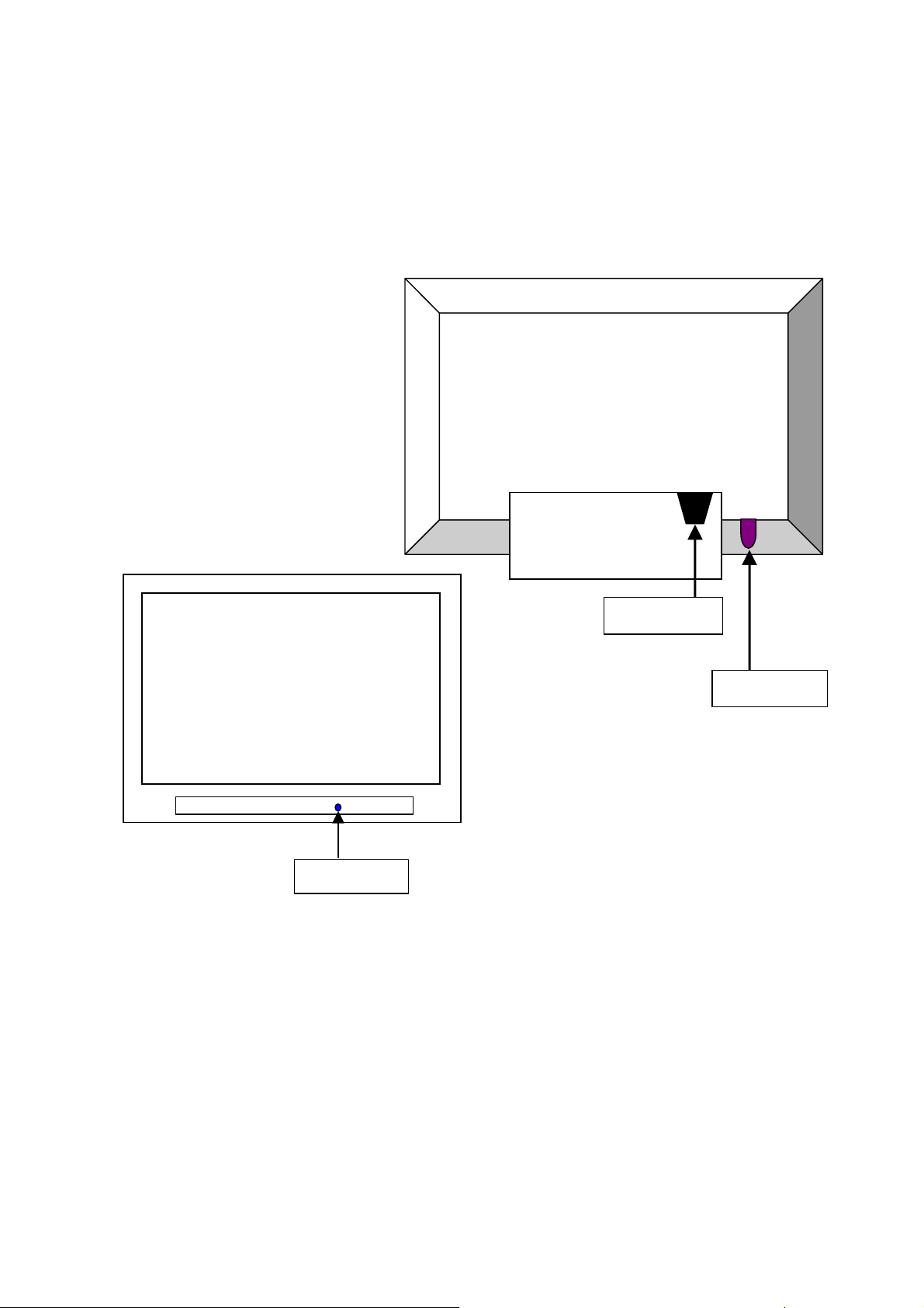
1-4-1 Power Indicator
42MFx30A/37 shall make use of an LED type indicator located on the front of the display. The
LED color shall indicate the power states as given in the following table.
LED colors
Mode H-Sync V-Sync Video Pw-cons. Indicator
Power-On On On Active
Standby Off Off Off
350W/ Blue LED
<
450W
<
1W Red LED
<
11
Page 12
1-4-2 Remote Control Receiver
42MFx30A/37 shall provide an infra-red (IR) optical detector on its front panel for use as the
receiver for remote controller signal. The IR communication protocol shall conform to RC-5
standard. The minimum IR reception angles shall be +/- 30 degrees horizontally and vertically.
The required operating distance of the remote control shall be 7 m.
1-4-3 On-Screen Display
42MFx30A/37 shall provide an On Screen Display (OSD) system for customer setup. The
following table gives the structure of the OSD menus.
Main menu Sub menu Function Default Reset
SETUP
Tuning Band
Signal Strength
Auto
Channel Search
Manual
Channel Set
To select between Terrestrial and Cable
System
To display the signal strength in order to aid
the antenna adjustment
To scan all TV channels and store them in
memory
Air —
— —
— —
To enable or disable channels — —
VIDEO
AUDIO
FEATURE
Channel Label To rename a channel — —
Manu
Language
To select the language for OSD among
English, Spanish, and French
English —
CONTRAST To adjust the contrast value between 0 and 63 50 Yes
BRIGHTNESS
SHARPNESS
To adjust the brightness value between 0 and
63
To adjust the sharpness value between 0 and
63
50 Yes
50 Yes
COLOR To adjust the color value between 0 and 63 50 Yes
TINT To adjust the tint value between 0 and 63 50 Yes
COLOR
Temperature
Aspect Ratio
To adjust the color temperature and white
balance.
To select aspect ratio among Nor mal, Zoom,
Wide, and Cinema
Yes
Normal Yes
Settings To restore all video settings to factory default — —
Audio
Language
To select audio language among English,
Spanish, and French
English Yes
BASS Sets the bass value between 0 and 63 31 Yes
TREBLE Sets the treble value between 0 and 63 31 Yes
BALANCE
Sets the left/right balance value between 0
and 63
31 Yes
Restore Default To restore all audio settings to factory default — —
Time Set To set current time — —
To set the timer period to turn off the TV.
Sleep Timer
Selectable values are OFF, 30, 60, and 90
OFF —
minutes
Password Set To set or change Parental Control password TBD —
Parental
Control
To select V CHIP settings Un-locked —
12
Page 13

1-5 External Mounting Requirements
42MFx30A/37 shall be designed so that the display enclosure can be easily removed from the
base for external mounting applications. When the base is removed, there shall be no additional
non-removable parts that are visible from the front of the display
1-6
Environmental Requirements
1-6-1 Temperature Ranges
Operating
Temperature (Independent of altitude) 42MF130A.................... 5°C to 35°C
42MF230A.................... 0°C to 40°C
Non-Operating Temperature (Independent of altitude)
42MF130A.................... -20°C to 60°C
42MF230A.................... -10°C to 85°C
1-6-2 Humidity
Operating (non-condensing)
.......................................................
Non-Operating (38.7°C maximum wet bulb temperature
42MF130A.................... 20% to 80%
42MF230A.................... 10% to 85%
42MF130A.................... 5% to 80%
42MF230A.................... 5% to 85%
1-6-3 Altitude
Operating
Non-Operating
................................................................................
......................................................................
42MF130A......... 0 to 6,562 ft. (0 to 2,000 m)
42MF230A......... 0 to 6,562 ft. (0 to 3,000 m)
42MF130A......... 0 to 9843 ft. (0 to 3,000 m)
42MF230A......... 0 to 9843 ft. (0 to 3,000 m)
1-6-4 Vibration and Shock
All testing shall be done in each of three mutually perpendicular axes, referenced to the position
of the system as it is in front of the user (i.e., front-to-back, side-to-side, and top-to-bottom).
2、、Precautions and Notices::
2-1
Precaution of assembly
(1)Please do not press or scratch PDP panel surface with anything hard.
(2)Please wipe out PDP panel surface with absorbent cotton or soft cloth in case of it being soiled
(3)Please wipe out drops of adhesive like saliva and water in PDP panel surface immediately. They might
mage to cause panel surface variation and color change
da
(4)Do not apply any strong mechanical shock to the PDP panel
2-2
Precaution of Operation::
(1)Please be sure to unplug the power cord before remove the back-cover. (make sure the power is turn-off)
(2)Please do not change variable resistance settings in PDP MODULE; They are adjusted to the most
suitable value. If they are changed, it might happen LUMINANCE does not satisfy.
(3)Please consider that PDP MODULE takes longer time to become stable of radiation characteristic in
mperature than in room temperature.
low te
(4)Please pay attention to displaying the same pattern for very long-time. Image might stick on PDP.
13
Page 14
3、Operation
m
y
r
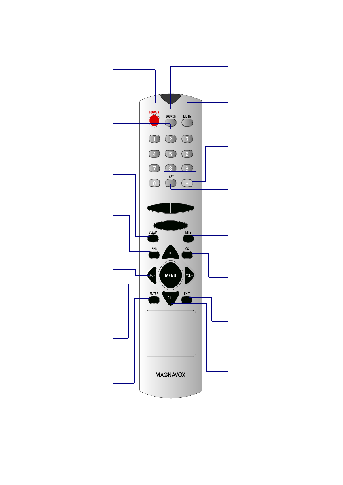
3-1 Operation of Remote Control Transmitter
42MFx30A/37 shall provide an IR remote controller as accessory.
To switch TV set between
power on and standby modes.
To enter TV channel number.
To Adjust sleep timer options.
To enter or exit Electronic
“VOL- ()/ VOL+()”
To decrease or increase the
sound volume. Also to navigate
left or right the Menu.
To enter Menu mode.
To enter sub Menu or sub
“POWER”
“0~9 number”
“SLEEP”
“EPG”
Program Guide.
“MENU”
“ENTER”
item.
14
“SOURCE”
To select input source.
“MUTE”
To mute the audio output.
“•(dot)”
To enter sub channel number.
“LAST”
To switch to the previousl
viewed channel.
“MTS”
To select audio progra
options.
“CC”
To select close caption options
(CC1, CC2 ...)
“Exit”
To exit Menu or other OSD.
“CH+ ( )/ CH – ()”
To select the next higher o
lower channel. Also to navigate
up or down the Menu.
Page 15

3-2 Front panel controls
⑦
⑥
⑤
④
③
②
①
②
- CH + - VOL +
IR: Remote Control Sensor.
Power switch: Press to power on or power off the TV set..
③ ● LED: Power Indicator.
MENU MODE
④ MODE Mode: Press to select input signal modes or use as Enter in Menu operation.
⑤ MENU Menu: Press to enter Menu or exit Menu.
⑥ -VOL+
Left: Press to decrease the sound volume level or move Left in Menu operation.
Right: Press to increase the sound volume level or move Right in Menu operation.
Down: Press to select the next lower Program number or move Down in Menu
⑦ -CH+
operation.
Up: Press to select the next higher Program number or move up in Menu
operation.
15
Page 16

3-3 OSD MENU Description
r
d
u
h
3-3-1 Main MENU
1. Press “MENU” key on remote control o
front panel controls to bring up Main Menu.
2. Press “ ” or “ ” to move the cursor up
and down the sub menu list.
3. Press “ ” or “” to select sub menu item.
4. Press "Enter" to enter sub-item then use
“ ” or “ ” to adjust.
3-3-2 SETUP MENU
1. Tuning Band: Select TV signal source
between Air and Cable. Select “Cable” if you
are connecting to a cable box and select
“Air” if you are directly connecting to the
antenna.
2.
DTV Signal: Display signal strength to aid
antenna adjustment.
3.
Auto Ch Search: Automatically scan an
store all TV channels.
Manual Ch Set: Enter channel setup table.
4.
5. Channel Labels: Display and edit channel
names.
6. Menu Language: Select language for men
(English Español).
DTV signal menu indicates signal strengt
in real-time.
Auto channel scan menu displays channel
number being scanned.
Manual Channel Set Menu
Displays
all the channel numbers that are
found.
Tune either to ATSC or NTSC channels.
Add or delete Channel number.
Channel Labels Menu allows user labeling.
16
Page 17
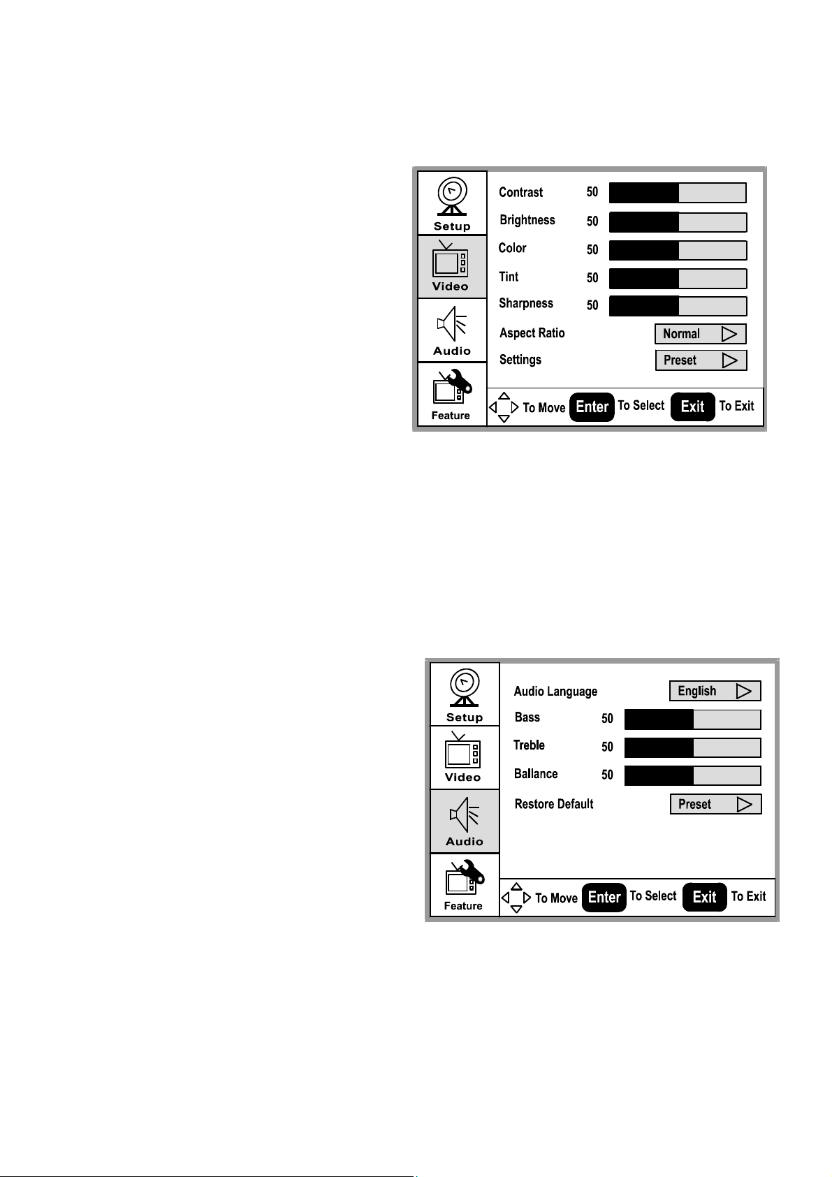
3-3-3 Video MENU
d
f
d
1. Press “” or “” to move the cursor up
or down the sub-item list.
2. Press "Enter" to enter the highlighte
sub-item menu.
3. Press “
” or “ ” to adjust the value o
the sub-item.
4. Press "Enter" again to exit the sub-item.
Contrast: Contrast adjustment, 0~100.
Brightness: Brightness adjustment, 0~100.
Color: Color chroma adjustment, 0~100.
Tint: Tint adjustment, 0~100.
Aspect Ratio: Aspect Ratio selection.
Normal
ZoomWide Cinema.
Settings: Restore default setting.
3-3-4 Audio MENU
1. Press “” or “” to move the cursor up
or down the sub-item list.
2. Press "Enter" to enter the highlighte
sub-item menu.
3. Press “
” or “” to adjust the value of
the sub-item.
4. Press "Enter" again to exit the sub-item.
Audio Language:
EnglishEspañolFrançais.
Bass: Bass adjustment, 0 ~ 100.
Treble: Treble adjustment, 0 ~ 100.
Balance: Balance adjustment, 0 ~ 100.
Restore Default: Restore Audio Language,
Treble, Base, and Balance setting to default.
17
Page 18

3-3-5 Featuree MENU
d
f
p
1. Press “” or “” to move the cursor up
or down the sub-item list.
2. Press "Enter" to enter the highlighte
sub-item menu.
3. Press “” or “” to adjust the value o
the sub-item.
4. Press "Enter" again to exit the sub-item.
Sleep Timer: Select minutes into standby
Off
30
60
90
.
Password Set: Enter and change Parental
Control Password.
Parental Control: Setup TV and Movie
rating controls.
Parental Control Menu: Controls
viewing of rated TV and Movie
rograms.
Note: Need password to change
settings. Default passwd = : 0000
3-3-6 Closed Captions
1. Press “CC” key on remote control to select closed captions mode.
NTSC TV: Off CC1 CC2 …
ATSC TV: Off CS1 CS2 …
2. Select desired closed caption mode.
NTSC TV
CC1
ATSC TV
18
CS1
Page 19

f
3-3-7 EPG
Press the “EPG” key on the remote control
to display the Electronic Program Guide
(EPG). A message window will be
displayed on screen.
3-3-8 TV channel arrangement
Each digital channel may comprise o
several sub-channels.
To select a digital channel using the remote
control:
1. Enter main channel number.
2. Press the “•” key.
3. Enter the sub-channel number.
EPG Message Window
Ch 5.4
19
Page 20
4、Trouble shooting chart
If replace “IMAGE BOARD”, Please re-do “DDC-content” program & “WHITE-BALANCE” & Flash
Update.
4-1 PANEL Trouble shooting
Please reference th e “PANEL Service Manual”.
4-2 Turn PDP on and Check:
Put the power switch after inserting the cable.
If PDP under the normal working, display of LED is blue. Then, the screen show is nor dark. If the color of
LED is red under standby state, you should press the “power” bottom of remote control or you should press
the front standby key. Then, turn PDP TV on.
If it is nothing about OSD or display on screen, service PDP.
The procedure and maintain the step meet as follows:
LED Light
20
Power Cable
Power Switch
Page 21
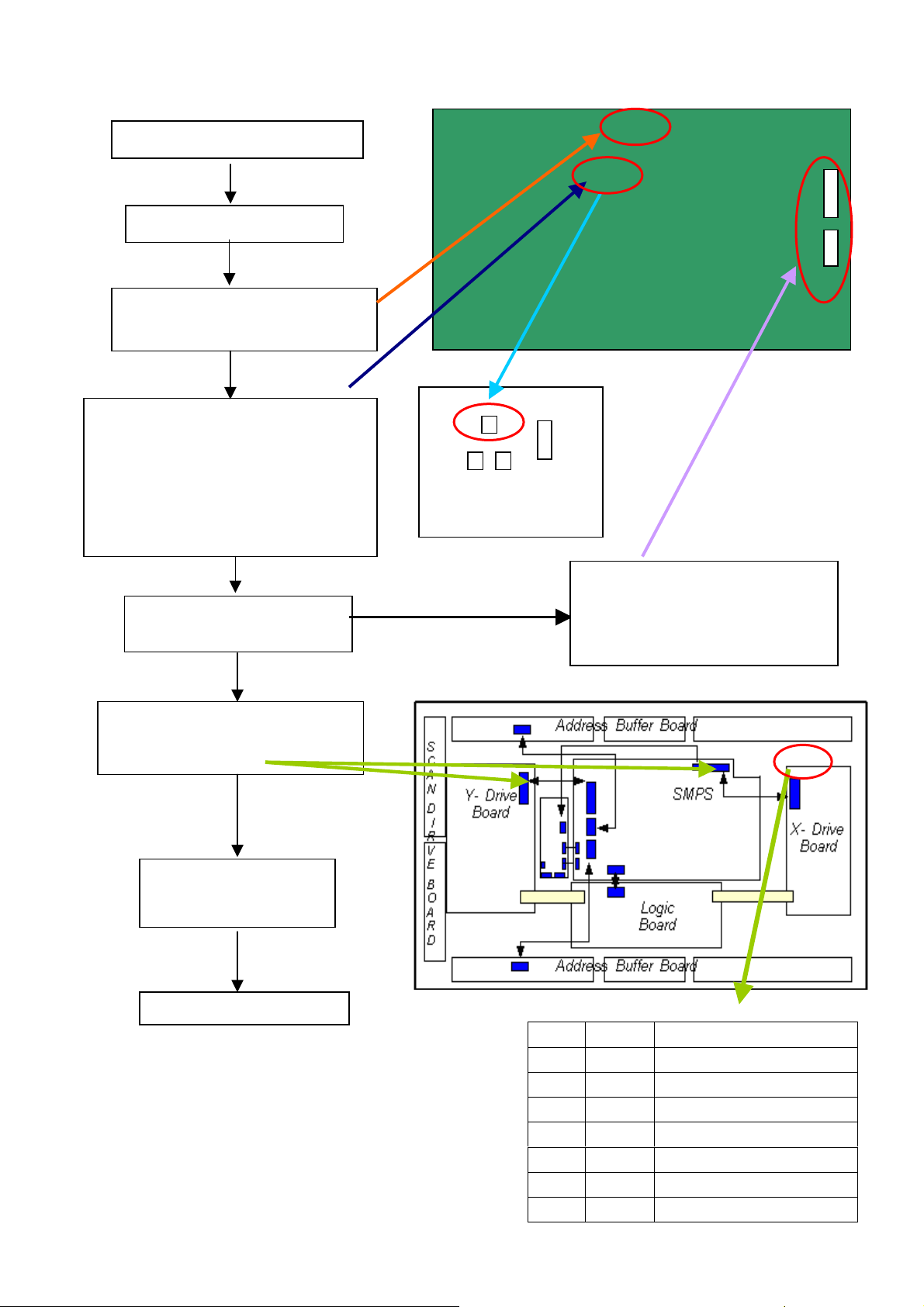
4-2-2 Solution process of whole PDP:
r
p
d
Screen is nothing under power on
Check AC input of PDC
Check PowerSTB5V(U516 3PIN)
Voltage: 5V
Check the REL-SW state of power IO
interface,
High Voltage:Turn on
Low Voltage:Standby
Test Point: C pole of Q5
High Voltage:5V(4.2---5.3V)
Low Voltage:0V
If REL-SW is ok,check othe
ower.
Check device circuit and logic circuit,
Vs, Vset, Vsc, Ve etc.
Arrow shows test point.
If there was anything
unmoral, test voltage an
repair it.
Process of repair as follow
U516
Q5
Image board
R128
CN703
CN704
Q5
Check the voltage of CN703:
PIN5 -- 12 V
PIN8 -- 3.3 V
PIN9 -- 3.3 V
--
Fig1: Voltage sheet
Name Voltage Reference
VS 170V Voltage for driving sustain
VA 70V Voltage for driving address
VE 155V Voltage for driving X-bias
VSET 160V Voltage for driving reset
Vscan -65V Voltage for driving scan
VCC 15V Voltage for driving FET
D3V3 3.3V Voltage for driving logic
21
Page 22
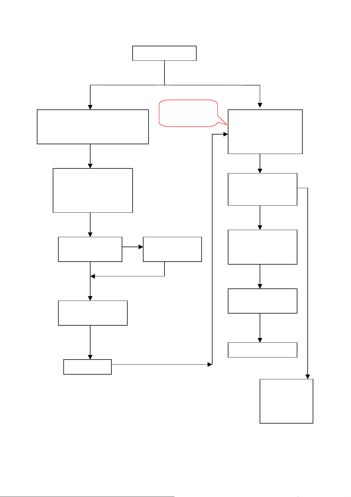
4-2-3 STB POWER Solution process
N
V
N
r
NG N
NG N
V
POWER un-moral
o input of +5VSB,or output is unmoral
Test point:CN903 PIN2
Voltage:5V(4.9-5.1)
Do these process
under the state is
+5VSB
out, or output is unmoral
Test point:CN902
Voltage: AC INPUT±1V
G
Test AC Input of CON901
ok or not?
Voltage:AC 100 V ~ 120
/200 V ~ 240 V
PS-ON ok or not?
Test point:CN903 PIN4
Voltage:DC5V(High)
Test voltage of C905
is DC300V or not?
OK
Check FUSE F901,
BD901ok or not?
Vccp ok?
Test pads of C909
Voltage:DC13V-25
Check IC901 and D901
ok or not?
OK
Q901, Q902, Q903, Q904,
M902 ok or not?
OK
AC POWER-OUT OK
+5VSB OK
Note:Must distinguish connect Grand point of Power primary and secondary level.
22
o input of AC Powe
G
OK
OK
OK
Check circuit of
IMAGE BOARD,
and check PS-ON
OK or not?
Page 23

4-2-4 Solution processes for DC Power
k
r
Check the junction that CN703 to
CN704 or CN701 to CN702 ok
or not?
Test input voltage:
L701 -- 12 V
L703 -- 6 V
L721 -- 3.3 V (Samsung PANEL)
OK
Test voltage as follow:
L705--8V
L706--5V
L704--5V
L718--2.5V
L719--1.2V
OK
4-2-5 Solution processes for SCALER
Check power supply , input
and output signal of U1
(ZR391055) and U2
(DS90C2501)ok or not?.
Check input and output signal of
U8,and TX0-/TX0+ signal etc. o
or not?
OK
OK
NG
23
NG
NG
Is there any short or
cold solder?
Is there any short o
cold solder?
Replace U8
Page 24

4-2-6 Solution processes VIDEO
N
r
r
r
N
N
N
o display under Video, S-video,
YCbCr and YPbPr mode
Check the state of powe
switch ,and DC power.
1.Test input signal of U14
under VIDEO and
S-VIDEO mode
2. Test input signal of U1
at C18/C19/C20 under
YCbCr mode
OK
Check U1
Check circuit of U6
(PW1231) ok or not?
OK
Check circuit of U20
(SCALAR)and LVDS
OK
OK
OK
G
G
G
Is there any short or disconnection,
and signal is wrong.
(The signal of standard color ba
will be very clea
Is there any short or disconnection, CLK
and SYNC signal to U1circuit?
Is there any short or disconnection, CLK
and SYNC signal to U6 circuit?
)
U6
X5
24
Page 25

5、White-Balance Adjustment
5-1 Equipments list
Chroma7100 1set
VG828 video signal generator 1set
Chroma-2326 1set
5-2 Preparation and Adjustment process
1、Preparation:
Connect rear Video port of PDP with AV port of VG-828.
Connect component port of PDP with YPbPr port of VG-828
Connect VGA port of PDP with corresponding port of Chrom2326
Turn power of PDP and test instrument on.
Before open lens, Press O-CAL of Chrom-7100 and revise lens.
2、Adjustment process
AV Adjustment
1). Change to Video mode, you can press “SOURCE” of remote. Press “Vol - ”, adjust volume
until Min. Then press number key “6543”and enter factory Menu.
2). Press “SOURCE” and change to Video Rear mode
3). When setting of VG-828 is TIM946/PAT922, 32 Gray steps. Then, see the color of picture
is deflection or not. And the Gray steps distinguish 28 steps from 32steps or not.
①. If dark of Gray is deflection, press “CH+/-”and adjust:
1.White.BRoCVBS (vMin=0,vMax=100,vDef=50) →50,
2.White.BBoCVBS (vMin=0,vMax=100,vDef=50) →50,
3.White.BGoCVBS (vMin=0,vMax=100,vDef=50) →50,
②. If sharpness of Gray is deflection, press “CH+/-”and adjust:
4.White.BRgCVBS (vMin=0,vMax=100,vDef=50) →50,
5.White.BBgCVBS (vMin=0,vMax=100,vDef=50) →50,
4). When the Gray is ok, change input signal to white picture at P936, Use colored analysis
instrument Chroma7100 measure colors temperature value of picture at present (whether
Chroma7100 is it given to picture center to pop one's head), On pressing the remote
controller such as the specification of going beyond "program + /- "key choose following
the projects adjust:
4.White.BRgCVBS (vMin=0,vMax=100,vDef=50) →50,
5.White.BBgCVBS (vMin=0,vMax=100,vDef=50) →50,
5). When adjustment about white is ok, changes signal to P822 that Gray steps picture. The
Gray picture has no deflection color, and the Gray steps distinguish 28 steps from 32steps
Note: The white balance is adjusted in the course, will influence each other to adjust in the
adjustment of gray steps and white picture, and need to change repeatedly.
Please notice that can't enter the mode of the factory in every station homework after adjusting
and finishing, so as not to miss movements and revise the white balance data again.
25
Page 26

VGA Adjustment
Setting of Chroma2326 as follows:
Gray picture: TIM4/PAT48
White picture: TIM4/PAT105
Change to VGA mode, press “CH+/-”and adjust following items. Method same as AV mode:
6. White.BRoVga (vMin=0,vMax=100,vDef=50) →50,
7. White.BBoVga (vMin=0,vMax=100,vDef=50) →50,
8. White.BGoVga (vMin=0,vMax=100,vDef=50) →50,
9. White.BRgVga (vMin=0,vMax=100,vDef=50) →50,
10. White.BBgVga (vMin=0,vMax=100,vDef=50) →50,
Note: Press “Source” and change mode that Video Rear to VGA, then adjustment items of
white balance same as Video Rear First, press “CH+/-” and adjust under the VGA mode.
(White.BBgCVBS(vMin=0,vMax=100,vDef=50)→50 CVBS change to VGA)
COMPONENT Adjustment:
1). VG828 setting as follow:
Gray picture:TIM954/PAT922
White picture:TIM954/PAT936
2). Change to COMPONENT1 mode,press “CH+/-”and adjust following items. Method same
as AV mode:
1. White.BRoVga (vMin=0,vMax=100,vDef=50) →50,
2. White.BBoVga (vMin=0,vMax=100,vDef=50) →50,
3. White.BGoVga (vMin=0,vMax=100,vDef=50) →50,
4. White.BRgVga (vMin=0,vMax=100,vDef=50) →50,
5. White.BBgVga (vMin=0,vMax=100,vDef=50) →50,
Adjustment stand of white Balance: x=299±15,y=315±15
6、DDC program and test
6-1 Equipments list and prepare
DDC tester 1PCS
PC 1set
D-SUB cable 1PCS
DVI cable 1PCS
Barcode reader 1set
Prepare before test:
1. Turn on the power of your PC and programmer, then make good connection of them.
2. Connect the D-SUB wire and DVI wire to the DDC program equipment and the PDP monitor.
6-2 Program and test process
1. Choose different DDC menu according to different customer , do use PAGE DOWN/PAGE UP to go to the
submenu and parent menu until find the right model. Press enter to access the program interface. There will
be shown RGB on the screen. Then switch to RGB program on the DDC connector。Press any key to access
RGB program interface ,then there will be “input serial no.:” prompt on the screen.
26
Page 27

2. Use Bar Readers to read the serial no to the program,then make sure the serial no you have read is the same as
on the barcode. Then set the PDP to blue screen mode, press enter to start.
3. Watch the information of the program, it means programmed OK when the following interface come out.
please CHECK Manufacturer Name、V endor Assigned Code、Model Name、Serial Number:
****[?????????****](same as Barcode)、Week of Manufacture:**、Year of Manufacture:****、Checksum:
**(same as the last byte of data table, reference to the note of RGB programming picture)and so on.
4. Press Enter to access RGB DDC test interface,follow the DDC test picture,CHECK Manufacturer Name、
V endor A ssigned Code、Model Name、Serial Number:****[?????????****](same as Barcode)、Week of
Manufacture:**、Year of Manufacture ****、Video Input:Analog、Checksum:**(same as the last byte
of data table, reference to the note of RGB programming picture)and so on.
5. Press any key to access DVI program interface, there will be “DVI” shown on the screen. Switch the of
switch on the DDC connector, press any key to access DVI program interface, there will be “input serial
no.:” promote.
6. Use Bar Readers to read the serial no to the program,then make sure the serial no you have read is the same
as on the barcode. Then set the PDP to blue screen mode, press enter to start.
7. Watch the information of the program, it means programmed OK when the following interface come out.
please CHECK Manufacturer Name、V endor Assigned Code、Model Name、Serial Number:
****[?????????****](same as Barcode)、Week of Manufacture:**、Year of Manufacture:****、Checksum:
**(same as the last byte of data table, reference to the note of DVI programming picture)and so on.
8. Press Enter to access DVI DDC test interface,follow the DDC test picture,CHECK Manufacturer Name、
V endor A ssigned Code、Model Name、Serial Number:****[?????????****](same as Barcode)、Week of
Manufacture:**、Year of Manufacture ****、Video Input:Analog、Checksum:**(same as the last byte
of data table, reference to the note of DVI programming picture)and so on。If the recording is failure, check
the connection of equipment and record again from the step4.If all of these work does not take work ,please
ask IE department for help.
9. Notice :the “?” and “*” symbol will be changed according to the year of manufacture ,and so on.
27
Page 28

7、、Flash Update
7-1 The list of Instrument
1、Prepare 1 piece of RS232 cable(The Pin connection see the Figure-1,If difference, please re-connect the
e)and 1 set of PC.
cabl
2、 Connect the RS232 cable with PC and PDP(See the Figure-2).
PC
PC
To
To
To PC
To PC
Pin (Female)
9 Pin (Female)
Signal Pin
Signal Pin
1
1
1
RXD 2
RXD 2
RXD 2
3
3
3
TXD
TXD
TXD
DTR 4
DTR 4
DTR 4
GND 5
GND 5
GND 5
DSR 6
DSR 6
DSR 6
RTS 7
RTS 7
RTS 7
CTS 8
CTS 8
CTS 8
9
9
9
Figure-1 Figure-2
7-2 The operation explaining Flash Update
Note: Operation Under the situation of PDP working normally.
The iDev is a Windows utility that installs hex files into the FLASH ROM of the target Image Processor
em. iDev is a Windows-based application.
syst
Downloading is done through an RS-232 connection, which is bidirectional and serial.
Step 1: Open the file iDev (You should
To Philips PDP
To Philips PDP
Philips PDP
Philips PDP
To
To
9 Pin (Female)
9 Pin (Female)
Signal Pin
Signal Pin
1
1
2 RXD Received Data
2 RXD Received Data
3 TXD Transmitted Data
3 TXD Transmitted Data
4 DTR Data Terminal Ready
4 DTR Data Terminal Ready
5 GND Signal Ground
5 GND Signal Ground
6 DSR Data Set Ready
6 DSR Data Set Ready
7 RTS Request To Send
7 RTS Request To Send
8 CTS Clear To Send
8 CTS Clear To Send
9
9
PC
PDP
RS232 Connector
RS232 Cable
28
Page 29

Step 2: Choose the director of the file to flash
Note: Connect the computer’s serial port (usually COM1) to the serial port of the ZORAN evaluation board
using a null modem cable, and select speed.
Step 3: Flash only the file required
29
Page 30

Step 5: Press reset or cycle the power from the Evaluation Board and click “down”
Step 6: View hex file flashing progress, after the files have been downloaded, Click “Close” to exit
30
Page 31

8、Software Platform Reference TV Application
8-1 Introduction
This document describes Phobos’s reference TV application, supporting the basic control functionalities
required to watch television. The reference application is designed to assist Phobos customers in implementing
a DTV system, using the Generation9-Elite IC and its APIs. This reference application is intended to support
U.S. based terrestrial analog/digital broadcasting(NTSC/ATSC), and includes Electronic Program Guide
(EPG), closed captioning, and parental control, as well as basic TV controls and underlying A/V decoding. The
reference TV application layer lies on top of Phobos’s Cougar API middleware that provides the
Transport/Audio/Video/graphics driver functionalities as a chip-independent set of APIs.
8-1-1 Supported Functions
The supported application functions are:
• Power control
• Source selection
• Channel change (up/down, recall and direct digit key input)
• Volume and mute control
• Closed caption selection
• Electronic program guide
• Menus: audio, video, setup, feature
8-2 The Phobos Reference TV Application
This chapter describes basic TV controls such as channel changing, source selection, and mute/volume control.
These basic functionalities are made available through the combination of GUI and standardized TV APIs. The
application also utilizes the results of PSIP parsing and decoding of EIA708/608 data. These are used to
support closed captioning and parental control, both of which are required on television sets sold within the
U.S.
In addition to Tuner, AV Input and Channel Map APIs, the reference application uses a set of Control
Array APIs to control the hardware blocks. These provide a standardized way to control the various hardware
blocks in the TV chassis.
8-2-1 Power Control
The current reference application does not support standby power control as part of this
implementation. Instead, pressing the power button on the remote and front panel controls the display and
audio outputs only. A power-on configures the system based on Control Array values stored in non-volatile
memory.
8-2-2 Source Selection
The Reference platform has analog/digital base band inputs as well as transport input through ATSC digital
channel. The TV/Input button cycles through the input sources:
1. RF
2. Front Composite (shared with S-video)
3. Rear Composite (shared with S-video)
4. YPbPr Component 1
5. YPbPr Component 2
6. VGA
7. HDMI input
The displayed banner for changing source is the same as the channel banner, except for displaying source
number and name.
31
Page 32

8-2-3 Channel Change
There are three ways to select a channel in the reference TV application: channel up/down, digital, and last
buttons in remote controller.
• Pressing the channel up or down key tunes to the next highest or lowest channel in the selected channel
map; a channel in a different channel group (analog or digital) is tuned at the limits of the available scan.
The channel map is established through the Auto Program menu, which automatically removes any no
signal channels. After channel scanning, the channels are grouped as digital channels and analog
channels.
• For digital channels, the channels are sorted on the virtual channel number. Further manual editing of the
channel list can be done through the Manual Channel Set menu. If no channels are enabled in the
selected channel map after initial power on, then the channel up/down keys select the channel number
next to the current channel, and determine the analog or digital channel based on the availability of
signal.
• Channels can be directly accessed by pressing the digit keys on the remote controller. The channel
selected is tuned immediately if the OK key is pressed, or will be tuned automatically after two seconds
of inactivity following the last entered digit. If the entered digit keys starts with a zero (“0”), the channel
number will be tuned to the second digit (for instance, the digits 03, entered in sequence, will tune
immediately to channel 3). Any channel may be selected by this method, regardless of its presence or
absence in the current channel map.
• Pressing the Last key in the remote control tunes the channel selected prior to the currently tuned
channel. For ATSC channels, it selects the sub-program number as well as the channel number.
The above channel-change operations are implemented via the Tuner and Channel Map APIs.
After tuning, the application displays the information of the currently-tuned channel. This includes:
1. Channel number [Ch 9-1]
2. Channel Label [for instance, KQED]
3. Current Time [for instance, 12:30 PM]
4. Rating information [for instance, TV-PG]
The virtual channel number will be displayed if the current channel is digital. The chann el la bel is extracted
from input signal if there is no label setting for the current channel. The channel label can be explicitly set with
Channel Labels menu, which will use TLChMapSetChannelName to store the label.
8-2-4 Volume and Mute Control
Pressing the volume Up or Down button changes the current volume in the Control Array and applies this
change to the hardware block. The range of control is determined by the Control Array; the current
implementation has a range from 0 to 63. Pressing either of the volume keys clears the mute audio mode of
operation, if previously set. If no button is pressed for five seconds after pressing the last volume Up or Down
button, the volume display will be automatically removed.
The reference application supports audio mute or un-mute by pressing the Mute key. When mute is enabled,
the audio is muted, displaying an icon on upper right side. The mute condition is cleared when the TV is
powered off.
Pressing the Mute key invokes the mute icon on the right corner of screen.
8-2-5 Closed Caption Selection
This section describes how to enable Closed Caption (CC) on the Phobos TV application. When the TV
is switched ON, captions are disabled by default. The user switches captions ON using the [SUBTITLE] key
on the remote. Each time the [SUBTITLE] key is pressed, a new language/CC option, is displayed near
the bottom center of the display. The sequence of options available are listed below
(depending upon the stream type — ATSC/NTSC).
For ATSC, English – Spanish – French – Off For NTSC, CC1 – CC2 – CC3 – CC4 – Off The displayed CC
option can be set either by the user pressing the [OK] key on remote, or else it is set automatically after two
32
Page 33

seconds.
8-2-6 Navigating a Menu
Pressing the Menu button displays the most-recently-used menu. The main menu is presented in two areas: a
group of icons, and a list of sub-menus based on the selected icon. After launching the menu, the Left/Right
buttons are used to select one of the two areas. The icons and sub-menus can then be navigated through the
Up/Down arrow keys, which moves the highlighted item up or down, depending on the key pressed. This
display gives the user a method of selecting among the various sub-menus available, in order to co nfig ure the
system.
The action wraps from first to last when an up arrow is received and the first list item is highlighted, and from
the last to the first when a down arrow is received and the last list item is highlighted. If no key is pressed for
one minute after pressing the last navigation or OK buttons, the volume display will be automatically
removed.
9、Block diagram & Explain
9-1 PDP b
J6 to Panel
Front AV PCB
lock diagram and functions
CN5008 to CN8003
CN4001 to CN8086
Panel
CN009 to J11
CN004 to J30
POWER PCB
CN8001 to CN902
CN904 to CN703
CN903 to CN704 & J603
CN706 to CN903
Image Board PCB
Power Down Control PCB
J42 to P210
Key Board PCB
Function of Board:
1) IMAGE Board : Control all input signals, Decode the video signal, De-interlace, and
send digital signals (LVDS signal) sent from image Board and display
2) PDC Board: Power Down Control Board
3) SIDE AV Board: The input signal interface
4) Power Board: Supply Power for Panel and Image Board
5) KEY Board: POWER, Signal Source, MENU, CH+, CH - / VOL +, VOL -
6) Power ON /OFF: Turn power on/off
33
Page 34

Part apt to decrease:
1) BEZEL, REAR COVER& GLASS FILTER
2)
Panel
3) Terminal Board’s RCA plug
9-2 Image board block diagram and signal introduce/process
9-2-1 Image board block diagram
34
Page 35

X
ATSC/NTS
C
V
TV
PDP Module
PDP Module
MPEG
l
Signa
Process
SCALER
Process
Analog
AV
Process
ideo / Audio block
ATSC/NTSC TV (Tuner)
Signal
Logic
(Memory Con
Y Con.)
X-
SMPS
Power
supply
Audio Process
Scan
Drive
PPDDPPPPaanneel
DATA Drive
Speaker
l
Scan
Drive
Y
9-2-2
Signal introduce/process
Panel
SDI-42HD
35
Page 36

ATSC+NTSC TV RF signal are separated into 2 way output when enter into Tuner. One is NTSC
(Analog signal) that output video signal by mixing, amplifying, demodulating. Video signal are
separated into Y/C signal throughTEA6415C, and transferred into ITU601 through ADV7401, then
send into Video-audio process chip Generation9. Tuner output SIF audio signal to MSP3450G to
process, amplify, then put in D-type amplifier TA2024.
The other ATSC (Digital signal, ATSC channel bandwidth is 6MHZ) via Tuner transferred into
TS-strea
m through 44MHZ intermediate frequency amplify, ASW filter, QAM\OFDM demodulate,
then enter into Generation-9 to MPEG decode, video part revert into video signal through coding,
and transferred into double-field TTL signal by this chip process. Then put into Scaler and LVDS
drive chip DS90C2501, through coding output 5 pair LVDS signal to drive PDP panel module.
Digital audio signal from Generation-9 revert into Audio signal to MSP3450G through PCM
decoding.
Program information in TS-stream be parsed and stored, user could know related program
information through OSD query menu. For multi-program TS-stream, user could appoint to see
some program in this stream through program guide EPG.
, S-video, YPBPR, DVI, D-Sub and each Audio signal through two group of 74HC4052
AV
switch with ATSC audio signal together put into MSP3450G, through alt, woof, balance, volume,
SRS, BEE process, then amplify by D power amplifier TA2024,output to loud-speaker.
36
Page 37

9-2-2 Input signal introduce
1. VIDEO: transmit bright & chroma signal , it is general ,its picture quality is equal to the general VCD.
S-VIDEO transmit the bright and the chroma single, and can reduce/control the cross-interfere , it is better
than the Video.
2. RGB&D-SUB(Pc interface ): general RGB simulative input interface .
3. YCbCr(NTSC/PAL): is composed of one bright and two chromatism signals U/V. due to the eye is more
sensitive for bright than chroma , RGB via the formulae Y=0.39R+0.50G+0.11B to transform into one bright
d two chromatism signals U(R-Y), V(B-Y).
an
4. VIDEO、、S-VIDEO、、YCBCR: the frequency 15.6KHZ 50(PAL)/60HZ(NTSC), interleaved simulative signal.
5. YPbPr: non-interlaced signal, belong to DTV scope, support 480P,720P,1080i format, current is NTSC.
6. DVI:digital Visual Interface, has 29pin(DVI-I)and 25pin (DVI-D), now many top grade display card own it.
10、、Waveform of signal
10-1 Waveform of input signal
YCbCr:
(Instrument outputs
Timing946 Pattern946 color bar picture
the sub board signal,,Instrument::VG828/ TG19CC/Oscillograph)
Y Luminance Signal R Red Signal
B Blue Signal
YCbCr: Timing 949 Pattern936 Full White Picture
37
Page 38

Y Luminance Signal
YCbCr:Timing 949 Pattern921 Gray Picture
Y Luminance Signal
YPbPr:Timing955 Pattern946Color Bar Picture
Y Luminance Signal R Red Signal
B Blue Signal
38
Page 39

YPbPr:Timing953 Pattern921 Gray Picture
Y Luminance Signal
YPbPr:Timing954 Pattern936 Full white picture
Y Luminance Signal
Video: Timing946 Pattern946 Color Picture Video: Timing949 Pattern936 Full White Picture
Video: Timing949 Pattern921 Gray Steps Picture
39
Page 40

S-video: Timing946 Patern946 color bar picture S-video: Timing949 Pattern936 Full white picture
S-video: Timing949 Pattern921 gray steps picture
10-2 Signal waveform in the image board
Video: Timing946 Pattern946 color bar picture
U14(Y/C separate)In (pin3 C136)/(pin20 C142)
40
Page 41

U14(Y/C separate)Out pin18/17 R119/R120
Video: Timing 949 Pattern936 white picture
U7 decoder output 8bit digital signal:
S-Video: Timing 946 Pattern946 color bar picture
U14 pin8, pin10
S-Video: Timing 949 Pattern946color bar picture
U7 8bit digital signal output:
41
Page 42

YCbCr: Timing946 Pattern946 Full white picture
Y signal—L55 R signal—L53
B signal—L54:
YCbCr:Timing 949、946 Pattern921、936、946 gray scale, color bar, white picture
U7 decoder output 8bit digital signal waveform
YPbPr: Timing 955 PATTERN946 color bar picture
Y signal—L55 R signal—L53
42
Page 43

B signal—L54
43
Page 44

11、Check and Measure
11-1 Image board
Test the power of each chip with the universal meter, to ground impedance and earth
situation.
11-1-1 Power Check and Measure
J603
Supply with getting red arrow point three interface J603, CN703 and CN704 that identification
come out for power, image of board with the interface among having picture, it corresponding
power make detection method separately among following several picture.: (Only for
SUMWUNG POWER)
①. In the following the first picture it is successively 1 to 6 pin of J603 from left to right:
Among them, 1pin and 2pin connect 12V voltage; 3pin, 4pin and 5pin are digital earth;
The second picture it is 1 to 5 pin of CN704 from left to right: Among them,2pin and
4pin of CN704 connect digital earth, 1pin of CN704 connect D6V voltage, 3pin of
CN704 connect D12V voltage ,The following picture shows:
CN703
CN704
44
Page 45

In the following picture it is
2
them
, The second pin connects STB5V,3pin 、6pin 、7pin and 10pin are grounded digitally,
5in connect D12V voltage, 8pin and 9pin connect D3.3V voltage,11pin connect D6V
voltage .The following picture shows:
11-1-2 Voltage value of IC necessary
Voltage Corresponding IC position and pin
U706 Pin3;
U704 Pin3;
U710 Pin3;
3.3V
U2 Pin38;
U9 Pin13;
U13 Pin3;
U10 Pin91;
CN703 Pin2;
E708;
STB5V
R301;
R635;
R68
L722,L713;
5V
L706,C718,E717;
CN706(PDC Board)
Pin2;
U709 Pin3;
6V
U702 Pin3;
U711 Pin3;
J603 Pin1,Pin2;
U701 Pin3;
R322;
12V
L702,E711;
CN703 Pin5;
L701;
successively 1 to 11 pin of CN703 from left to right. Among
D40 Pin5;
D41 Pin5;
U68 Pin3;
U30 Pin3, Pin1;
J32 Pin7;
U48 Pin26;
U52 Pin20
TP9;
R126,R128;
L216,L217;
R301,R635,R638
CN703 Pin10;
L703;
C702
TP8;
U601
Pin29,Pin30,Pin33;
C700;
U602 Pin8;
U12 Pin2,Pin4;
C695
45
Page 46

11-2 SIDE AV Board
The picture below is AV SIDE board, The interface pointed out in order to provides the power
for Audio board. The enlarged interface picture show in its connection.
CN004
Shown order connect power(it depends on to be 1 pin to 10 pin from left to right) according to
the picture:
11-3 PDC Board
The following picture show PDC Board, among them getting red difference label about
connection with PDC Board and main board, power board and switch of board.
CN901: Connect with P9Z1 of Power Switch Board;
CN902: Connect with CN8001 of Power Board;
CN903: Connect with CN706 of Imager Board.
CN903
CN901
CN902
The following picture shows the pin connection of CN903:
46
Page 47

12、Mechanical Introduction
12-1 PDP Internal view
47
Page 48

12、Mechanical of cabinet front disassembly 42MF130A
48
Page 49

12-2 Mechanical of cabinet front disassembly 42MF230A
49
Page 50
12-3 Disassembly and assembly
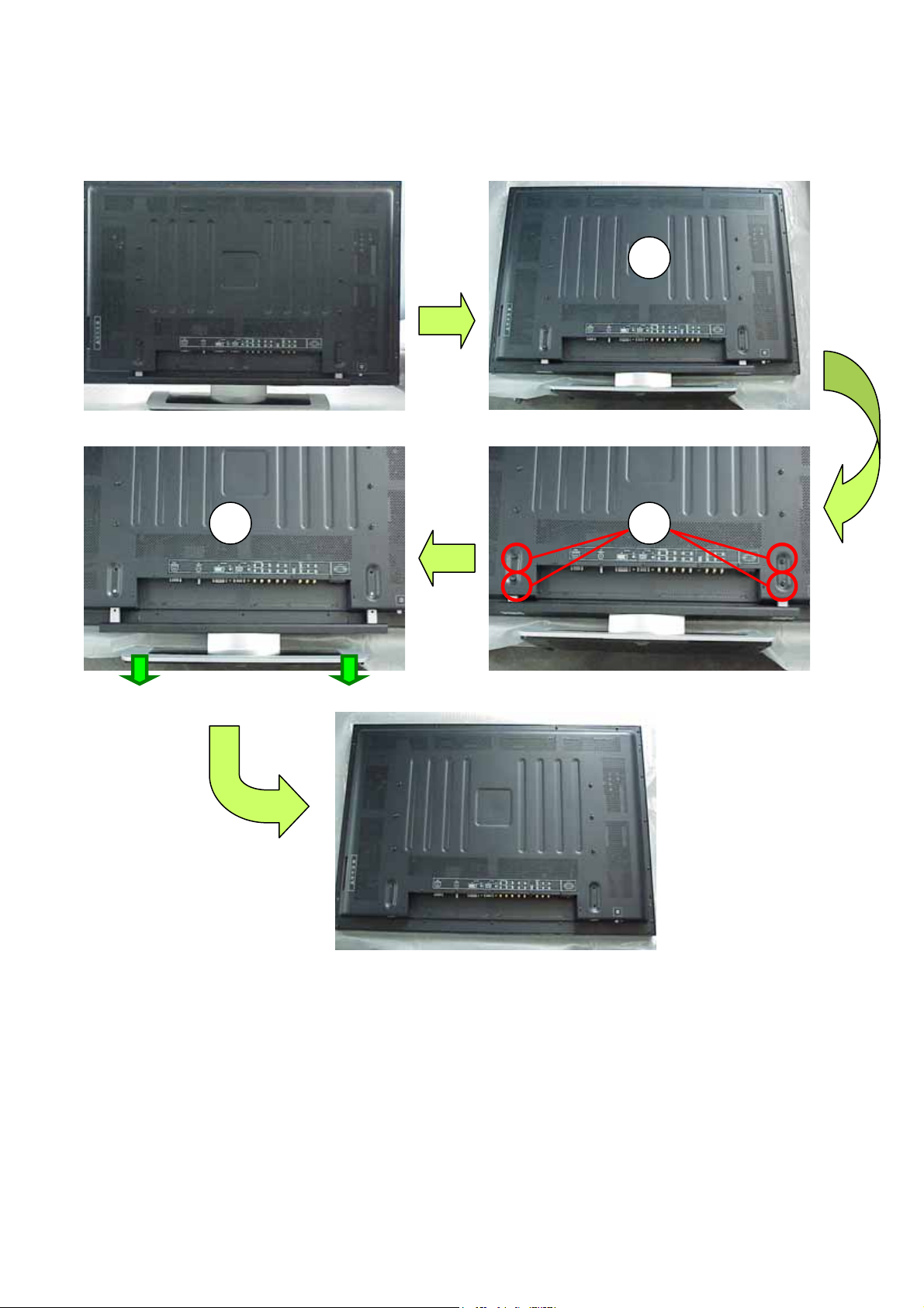
12-3-1 PDP stand removal
1) Unplug the AC power and all signal cables.
2) Place the PDP upside down on a tabletop (use a protection sheet or EPE bag), Take care, that this
is flat and free from obstacles like screws, to prevent damaging the fragile PDP glass filter (1).
3) Remove the four black colored screws around the stand holder (2).
4) Remove the Base assembly from PDP as the direction arrowhead showed (3).
3 2
50
1
Page 51

12-3-2 Back Cover Removal
5) Remove the six big black colored screws in the panel holder as the red-circle showed (1).
6) Remove the seven black colored screws around the terminals as the green-pane showed (2).
7) Remove the eighteen black colored screws around the back cover as the blue-pane showed (3).
5) Carefully prize up the back cover from
the left of the PDP (5).
z Don’t remove the cover in this st
ep, otherwise, the power button
should be damaged.
6) Carefully remove the Back Cover from the
top of the PDP, and store in a safe place.
5 4
3
1
2
Push
4) Push in the power button before remove the
back cover(4) (to prevent damaging the
power button).
7) Done.
Notes: Must be press down the power button before remove the back cover, if don’t do this it
well be avert broken switch at the remove the back cover.
51
Page 52

3
12-3-3 Rear Low Cover removal
1) Remove the three black screws in Rear low cover (1).
2) Carefully use a allen screwdriver to remove the six silver colored allen screws M3*6mm (2).
3) Remove the five black screws (3).
5 4
ZOOM-1 ZOOM-1
2
6
1
4) Remove the one silver screws and remove the
GND cable (4).
5) Disconnect the AC cable from AC FILTER
Board (5).
6)Remove the Rear Low Cover as the
direction arrowhead showed (6).
7)Done.
52
Page 53

12-3-4 Main Board(MGPC) removal
1) Disconnect the all connectors(J42,CN706,J14,J603,CN703,CN704,J11,J30 and J6 form M
GPC(main board). See the above figure.
2) Remove the six silver screws from MGPC(main board)(1).
3) Remove the MGPC board from PCB plate. 4) Done.
1
PCB Plate
J6
1
53
Page 54

12-3-5 PCB Plate Removal
1 2
4
3
1) Remove the two Cable Clips from the PCB Plate(1)(2).
2) Remove the six sliver screws(3).
3) Cut the cable tie(4), Note, please carefully cut it, don’t make the cable damage.
4) Remove the PCB Plate
54
Page 55

12-3-6 Key Board Remove
1) Remove the four silver screws(1).
2) Pull the Bezel downside(2), then push and take out the KEY board
assembly(3).
3) Remove the five silver screws to disassemble the key board from Key button.
Pull
Push and take it out
3
2
55
Page 56

12-3-7 Side AV Board Removal
1) Remove the two silver screws (1).
2) Remove the side cover from Side AV board(2)
3
3) Disconnect the CN004 and CN009 from Side AV board.
4) Remove the four silver screws (3).
2
CN004
1
CN009
3
56
Page 57

12-3-8 PDC(power down control)Board Removal
Panel
stand
Panel Holder
ZOOM 1
1 2
1) Remove the four sliver screws (1) and remove the panel stand from panel holder as
the direction arrowed showed.
2) Remove the four silver flat screws (2).
3) Remove the two black screws (3)
4) Remove the two silver screws (4)
5) Remove the panel holder from PDP.
CN903
5
CN901
CN902
ZOOM 2
2
3
4
6) Disconnect CN901,CN902 and CN903 from PDC
board.
7) Remove the four sliver screws (5), and remove
the PDC board.
57
Page 58
12-3-9 Panel Module Removal
1) Remove the eight silver flat screws around the two panel holder (1).
ZOOM 1 ZOOM 2
1 1
1
ZOOM 3 ZOOM 4
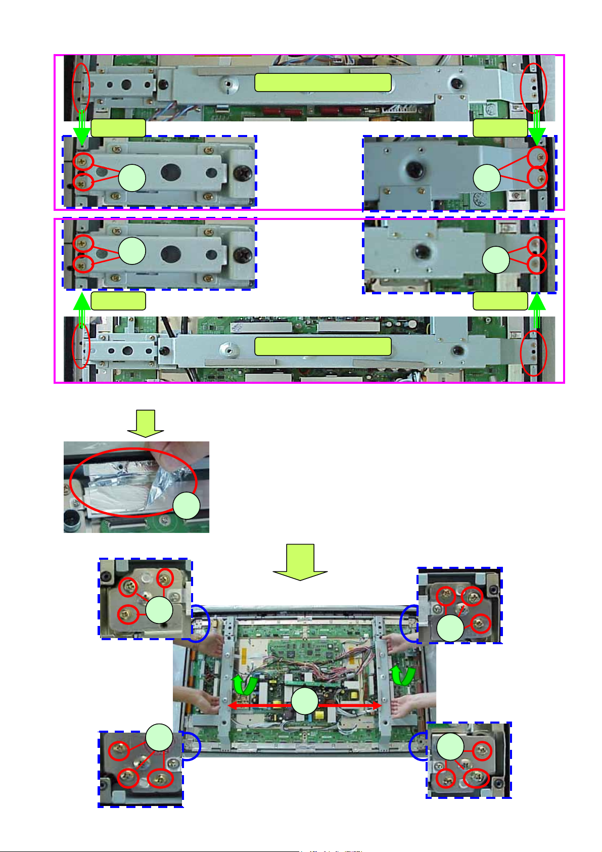
2) Remove all the aluminum foil around the panel (2), after assemble
the new panel, must re-affix the aluminum foil, if it’s broken
must change a new one, otherwise, the EMI can be affected.
3) Remove the twelve silver screw around the PANEL corner (3).
2
4) Two people hold the panel holder 1 and 2 respectively, then uplift
the panel module and move it out form the front cover(Bezel),
and store in a safe place.
3
3
Panel Holder-1
Panel Holder-2
4
1
3
3
58
Page 59

12-4 Block Wiring diagram
12-4-1 PDP boards block wiring diagram
Internal speaker
Internal speaker
Internal speaker
Internal speaker
Internal speaker
Left
Left
Left
Left
Left
Sub-PSU
Sub-PSU
Sub-PSU
Sub-PSUSub-PSU
PANEL Module
PANEL Module
PANEL Module
PANEL Module
Main PSU
Main PSU
Main PSU
Main PSUMain PSUMain PSUMain PSU
CN706
CN706
CN706
J42
J42
J42
J42
CN706
J14 J603
J14 J603
J14 J603
J14 J603
J6
J6
J6
J6
Power
Power
Power
Power
input
input
input
input
PDC B/d
PDC B/d
PDC B/d
PDC B/d
AC output
AC output
AC output
AC output
Internal speaker
Internal speaker
Internal speaker
Internal speaker
Internal speaker
Right
Right
Right
Right
Right
CN902CN903
CN902CN903
CN902CN903
CN902CN903
CN901
CN901
CN901
CN901
Power filter B/d
Power filter B/d
Power filter B/d
Power filter B/d
CN004
CN004
CN004
CN004
CN009
CN009
CN009
CN009
Side AV B/d
Side AV B/d
Side AV B/d
Side AV B/d
Image board
Image board
Image board
Image board
Image board
Image board
Image board
Image board
Image board
Image board
Key board
Key board
Key board
Key boardKey board
CN703
CN703
CN703
CN703
CN704
CN704
CN704
CN704
J11
J11
J11
J11
J30
J30
J30
J30
Socket
Socket
Socket
Socket
59
AC in
AC in
AC in
AC in
AC input
AC input
AC input
AC input
output
output
output
output
input
input
input
input
AC switch B/d
AC switch B/d
AC switch B/d
AC switch B/d
Page 60

No. Pin Connection Name Pin function
J42 Connector(13 Pins):
Pin 1= GND Pin 2= +5VSB
Pin 3= IR Pin 4= ENTER
J42 to Key board
1
MGPC key control signal
output
Pin 5= LED-B Pin 6=LED-A
Pin 7=KEY6 Pin 8=CH+
Pin 9= CH- Pin 10=VOL+
Pin 11=VOL- Pin 12=MENU
Pin 13=TV video
CN706 Connector(4 Pins):
Pin 1,3= GND Pin 2=+5VSB
Pin 4=REL-SW
CN903 Connector(4 Pins):
Pin 1,3= GND Pin 2=+5VSB
CN706 to CN903
2
PDC board DC output, and
MGPC standby PDC power
control output
Pin 4=PS-ON
J14 to speaker MGPC audio signal output
3
J14 Connector (2 Pins+2 Pins):
LO+/COMLO- and RO+/COMRO-
J603 Connector(6 Pins):
J603 to Sub-PSU
4
MGPC audio circuit power
input
Pin 1,2=+12V Audio
Pin 3,4,6=GND
Pin 5 = NC
CN703 Connector(11 Pins):
Pin 1=NC Pin 2=STB5V
Pin 4=Relay-SW Pin 5=D12V
Pin 8,9=D3.3V Pin 11=D6V
CN703 to Sub-PSU
5
MGPC power input and
relay control output
Pin 3,6,7,10 =GND
CN704 Connector(5 Pins):
CN704 to Sub-PSU MGPC power input
6
Pin 1=D6V Pin 3=D12V
Pin 2,4=GND Pin 5=NC
J11 Connector(5 Pins):
J11 to CN004 To Earphone output
7
Pin 1,3=GND Pin 2=EAR-L
Pin 4 = EAR-R Pin 5=Phone-on
J30 Connector(10 Pins):
Pin 1,3,5,9=GND Pin 2=CVBS IN-2
J30 to CN009 Side AV signal input
8
Pin 4=FRONT-Y Pin 6=FRONT-C
Pin 7=FRONT-AV-SEL
Pin 8=SM-L Pin 10=SM-R
J6 LVDS connector(31 Pins):
Pin 1,8,9=NC
Pin 2,4,6,11,14,15,18,19,
J6 to Panel Logic
9
b/d
MGPC LVDS signal output
22,23,26,27,30,31=GND
Pin 12=TXE3p Pin 13=TXE3m
Pin 16=TXECp Pin 17=TXECm
Pin 20=TXE2p Pin 21=TXE2m
Pin 24=TXE1p Pin 25=TXE1m
Pin 28=TXE0p Pin 29=TXE0m
60
Page 61

61
Page 62

13、PCB LAYOUT
13-1 Image board PCB LAYOUT
62
Page 63

13-2 Audio board PCB LAYOUT
63
Page 64

13-3 Tuner board PCB LAYOUT
13-4 Key board PCB LAYOUT
64
Page 65
DEL
B
A
N
E
n
o
itarepO daeR
-
o
tu
A nO
-rewo
P
TU
O -
3R
.)YLNO
M
6
5
2 gnu
sm
aS rof
(
e
lu
doM
VTD s
no
i
tpO g
niffu
tS
x
e
dnI tee
h
S
t
ee
hS elti
T
- 1
0
e
g
a
P
F
/
I
suB
l
acoL - 20 eg
a
P
F
/I
0
M
AR
D
S
RD
D
- 3
0 e
g
a
P
rotalu
domeD
/
re
nuT - 40
eg
aP
n
I o
id
uA
/ o
ed
iV - 50
eg
aP
F/I
I
MDH
-
60
eg
a
P
st
up
n
I oed
i
V
go
la
n
A -
70
e
gaP
F/I
t
ro
psnarT/redoceD - 80 egaP
e
cafretnI oe
d
i
V - 01 e
g
a
P
e
ca
f
r
e
tn
I
o
i
duA
- 11
e
ga
P
t
e
s
eR
/
O
X
CV /
O
I
S
- 21 e
g
aP
k
c
o
l
B
sOI
P
G
/
de
su
n
U
-
31 egaP
s
r
otc
e
n
n
o
C
GATJ/yt
i
l
i
t
U -
41
e
gaP
1
d
n
G
dna
re
wo
P
-
51
eg
aP
2 d
n
G
dna
r
e
w
o
P - 61
eg
a
P
.gni
t
tes t
luafeD -
*
:eto
N
3
dn
G
dna re
woP -
71
eg
a
P
4
dn
G
dn
a
r
e
wo
P -
81
ega
P
5
d
n
G
d
na
re
wo
P
-
91
eg
aP
noitceleSec
iveD tooB
=
]42,
3
2,2
2[J
kcolc ICP LANR
E
TXE htiw
eciv
ed atad tib-8 B
L mo
rf toob = 111
kcolc I
CP LA
NR
E
TXE htiw ec
ive
d
atad ti
b
-
6
1 BL
mor
f t
o
o
b = 01
1
ecived
z
HK
004
sserdda tib-61
C2
I mor
f
toob = 1
01
ecived
z
HK
001
sserdda t
ib-61 C2I morf
toob
= 001
)z
H
M
72( kcolc IC
P
l
anretni hti
w
eciv
e
d ata
d t
i
b-8 BL
m
o
rf toob = 110
)
z
H
M 72(
kcol
c IC
P lanret
ni htiw ecived ata
d tib-61
BL m
o
rf
t
oob = 010
k
col
c
z
HM 1 ,eci
v
ed atad ti
b-8 /s
s
e
rdda tib
-
42 I
PS morf toob = 100
k
colc zHM 1 ,eciv
ed atad ti
b-8 /sserdda tib
-61 I
PS morf toob = 000
s
noitp
O
r
ep
muJ dra
o
B ytil
itU
)A
)
B
edom GATJE - FFO
- 7
2
J
edom G
ATJ
-
NO
- 72J
)
2
*
.yln
o
dr
a
o
b
D&R r
o
F-
N
I - 8
1P
T-
1P
T
.
ver dra
o
b lani
f roF
-
TU
O
-
81PT-
1P
T
)1
1
SC -
hs
alFatart
S
42U
,0S
C
- hs
alF 32U -
-
3-
2 -
02
J ,NO -
61J
0
S
C - hsalFatartS 42U ,.
c
s
iD S
C - hsalF 32U -- 2-1 - 02J ,FF
O - 61J
)
3
.deretla eb ton
nac stnetnoc y
romem hsalFatartS
42U
- ,
NO - 7
1J
,ed
o
m
61x
ni
ecived hsalFatartS - FFO
- 81J
)
5
.ed
om 8x ni ecived
hsalF
atartS -NO - 81J
)
4
el
ba
T
s
OI
P
G
-
02
eg
a
P
SD
V
L
/ emi
rP
oe
d
i
V -
90
e
g
aP
*
.
IP
S morf
p
u-t
o
o
b la
mr
oN
TUO
-
8R
,N
I -
7R
)
C
.hsa
lf DN
AN morf
pu-tooB NI - 8R ,T
U
O
-7R
)
D
*
TUO - 82
5R ,5
2
5R
.putes
slevel
t
hgilkcaB DCL - N
I - 825
R
,525
R
*
sCAD
9G
rot ferV lanr
o
t
xE
-
-
TUO - 685R
,
485R
,N
I
- 58
5R
,38
5R,94
D
*
s
CA
D 9
G r
ot f
er
V
lanrotnI -- N
I
- 68
5R
,48
5R ,TUO - 58
5R,38
5R,94D
)E
D
ELBA
SID
n
oitare
pO daeR
-ot
uA
nO-rew
oP
TUO
-
3R
*
.)
Y
LNO M652
g
nu
sma
S r
of
(
.elb
ane drac yti
litU 232SR
,N
I - 34
3R ,243R
)
F
.e
lb
a
ne
rotcennoc kniL-G ,TUO - 3
43R ,2
43
R
)de
tats e
s
i
wrehto
ss
elnu
(
:
setoN
.1
.2
.3
.4
%
5
er
a
dna s
m
h
o
ni d
e
t
s
i
l
e
r
a
srot
s
i
s
e
r
l
l
A
)
r
otca
f
m
rof
3
0
6
0
( m
l
iF
lat
eM
,
61
/
1
,
)rotcaf
mrof 306
0(
R7
X
,c
imar
ec
,V
52 ,%
0
1 er
a dn
a
,s
dar
a
f
orc
i
m
ni
d
e
t
s
i
l
era s
r
o
t
ica
p
ac
llA
,
se
ir
ne
h
o
rcim
n
i d
e
t
s
i
l
er
a
srotcu
d
n
i
l
lA
)rotcaf mrof 50
80
(
d
nuow
-n
o
n ,am001
,%5
er
a
dn
a
.
steehs nee
wt
e
b
n
o
itis
nar
t d
na ,
l
a
b
olG e
r
a
s
r
o
t
c
e
n
noC
e
ga
P
ffO
d
n
a
s
t
r
o
P l
a
n
g
i
S
ro stroP
la
ng
i
S
tu
oh
t
i
w
s
emaN
la
n
g
iS
.5
tcennoc ylno dna ,la
c
oL
e
ra
s
rot
c
e
n
noC
e
g
a
P
ffO
.te
eh
s
e
m
a
s
e
ht
n
o
s
l
an
g
i
s
d
ema
n
e
k
i
l
Image Board
65
Page 66

5
U1A
ZR391055
PCI Bus Interface
LBUS_A3
LBUS_A2
LBUS_A1
LBUS_A0
(Local Bus)
LBUS_A19
LBUS_A18
LBUS_A17
LBUS_A16
LBUS_A15
LBUS_A14
LBUS_A13
LBUS_A12
LBUS_A11
LBUS_A10
LBUS_A9
LBUS_A8
LBUS_A7
LBUS_A6
LBUS_A5
LBUS_A4
LBUS_D15
LBUS_D14
LBUS_D13
LBUS_D12
LBUS_D11
LBUS_D10
LBUS_D9
LBUS_D8
LBUS_D7
LBUS_D6
LBUS_D5
LBUS_D4
LBUS_D3
LBUS_D2
LBUS_D1
LBUS_D0
LBUS_A3
LBUS_A2
LBUS_A1
LBUS_A0
RP2D 10Kx4
4 5
RP1A 10Kx4
1 8
RP3B 10Kx4
2 7
RP1D 10Kx4
4 5
RP1C 10Kx4
3 6
RP1B 10Kx4
2 7
RP3A 10Kx4
1 8
RP3D 10Kx4
4 5
RP2B 10Kx4
2 7
RP3C 10Kx4
3 6
R12 10K
RP2C 10Kx4
3 6
RP2A 10Kx4
1 8
PAR
IDSEL
AD14
AF11
AE14
AC9
AF14
AE5
AD15
AF5
AF15
AE6
AF16
AD9
AE16
AC11
AF17
AB10
AC13
AF18
AD13
AD18
AE15
AF20
AC15
AF19
AB17
AF22
AE20
AC18
AF21
AB18
AD19
AC19
AD11
AC14
AD17
AE18
AE19
AE11
AC17
AD10
AD16
AE12
AC16
AE17
AC10
AE13
AF8
AD12
AF10
AF12
AF13
AC12
AE10
AF7
AE9
AE7
AE8
AD8
AF9
LA19_AD31
D D
C C
B B
ZR391055SH
LA18_AD30
LA17_AD29
LA16_AD28
LA15_AD27
LA14_AD26
LA13_AD25
LA12_AD24
LA11_AD23
LA10_AD22
LA9_AD21
LA8_AD20
LA7_AD19
LA6_AD18
LA5_AD17
LA4_AD16
LAD15_AD15
LAD14_AD14
LAD13_AD13
LAD12_AD12
LAD11_AD11
LAD10_AD10
LAD9_AD9
LAD8_AD8
LAD7_AD7
LAD6_AD6
LAD5_AD5
LAD4_AD4
LAD3_AD3
LAD2_AD2
LAD1_AD1
LAD0_AD0
LA3_CBE3_n
LA2_CBE2_n
LA1_CBE1_n
LA0_CBE0_n
FRAME_n
PERR_n
TRDY_n
IRDY_n
STOP_n
DEVSEL_n
SERR_n
PCICLK
INTA_n
INTB_n
INTC_n
INTD_n
REQA_n
GNTA_n
REQB_n
GNTB_n
REQC_n
GNTC_n
REQD_n
GNTD_n
RST_n
4
LBUS_A[0:25]
3
2
LBUS_A[0:25]
R1 10K
R2 10K
U1E
LBUS_RDY0
LBUS_RDY1_n
1
+3.3V
ZR391055
LOCAL BUS
PINS (Dedicated)
LBUS_RD_n
LBUS_WRH_n
LBUS_WRL_n
LBUS_AS_n
LBUS_RDY0
LBUS_RDY1_n
LBUS_CS0_n
LBUS_CS1_n
NAND_CS2_n
LBUS_CS3_n
LBUS_CS2_n
LBUS_D[0:15]
Stuffing Options
+3.3V
R3
10K_NS
LBUS_RD_n
LBUS_WRH_n
LBUS_WRL_n
LBUS_AS_n
LBUS_RDY0
LBUS_CS0_n
LBUS_CS1_n
LBUS_CS3_n
LBUS_CS4_n
LBUS_CS5_n
LBUS_CS2_n
GPIO125
+3.3V
GPIO104
GPIO112
GPIO113
GPIO107
GPIO119
GPIO120
GPIO108
GPIO121
GPIO109
GPIO110
GPIO122
GPIO123
HDMI_VSYNC
CVmix_SEL
HDMA_SCDT
TV_VIDEO
HD_SEL
IDE_HSCBL_n
AIN_INT_n
ACLK_SEL0
ACLK_SEL1
FMS_SEL
CEC
SLEEP_MODE_n
TO Page 7
SEL
LBUS_D[0:15]
Stuff option.
NAND_CS2_n
NAND_GPIO1_n
R9
10K
R11
0_NS
LBUS_A25
LBUS_A24
LBUS_A23
LBUS_A22
LBUS_A21
LBUS_A20
R7 0
R8
0_NS
WP_n
LBUS_WRH_n
+3.3V
C1
0.1uF
AA7
AF4
AD7
AB9
AF6
AC6 AC7
LBUS_D7
LBUS_D6
LBUS_D5
LBUS_D4
LBUS_D3
LBUS_D2
LBUS_D1
LBUS_D0
LBUS_AS_n
LBUS_CS2_n
LBUS_RD_n
LBUS_WRL_n
LBUS_RDY0
LA25
LA24
LA23
LA22
LA21
LA20 LREADY0
ZR391055SH
LREADY1_n
NAND FLASH
44
I/O_7
43
I/O_6
42
I/O_5
41
I/O_4
32
I/O_3
31
I/O_2
30
I/O_1
29
I/O_0
16
CLE
17
ALE
9
CE
8
RE
18
WE
19
WP
7
R/B
12
Vcc1
37
Vcc2
C2
0.1uF
6
GND
13
GND
36
GND
NAND128W3A0AN1
LRD_n
LWRH_n
LWRL_n
LAS
LCS0_n
LCS1_n
LCS2_n
LCS3_n
LCS4_n
LCS5_n
U2
NC1
NC2
NC3
NC4
NC5
NC6
NC7
NC8
NC9
NC10
NC11
NC12
NC13
NC14
NC15
NC16
NC17
NC18
NC19
NC20
NC21
NC22
NC23
NC24
NC25
NC26
NC27
LOCK
AC5
AD5
AC8
AE4
AD6
AE3
AE2
AB8
AB7
AC4
AF1
1
2
3
4
5
10
11
14
15
20
21
22
23
24
25
26
27
28
33
34
35
39
40
45
46
47
48
38
A A
+3.3V
5
R29 10K
R27 10K
R28 10K
LBUS_A20
LBUS_A25
LBUS_A24
Title
Phobos
Size Document
B
Local Bus I/F
4
3
2
BOBCAT_D1_Plus.DSN
Sheet
222
of
Monday, March 28, 2005
Date:
Drawn by: O. Marinovsky
1
Rev
D2
66
Page 67

5
DDR0A[0:12]
4
3
2
U3A
1
DDR SDRAM
D D
U1C
ZR391055
DDR SDRAM 0
DDR0A0
DDR0A1
DDR0A2
DDR0A3
DDR0A4
DDR0A5
DDR0A6
DDR0A7
DDR0A8
DDR0A9
DDR0A10
DDR0A11
DDR0A12
DDR0BS0
C C
B B
DDR0BS1
DDR0DQS0
DDR0DQS1
DDR0DQS2
DDR0DQS3
DDR0DM0
DDR0DM1
DDR0DM2
DDR0DM3
DDR0RAS_n
DDR0CAS_n
DDR0WE_n
DDR0CK DDR0DQ29
DDR0CK_n
DDR0CKE
VREF
RP14D15x4
RP10C15x4
RP17C15x4
RP12D 15x4
RP7D 15x4
RP21C 15x4
RP19C 15x4
RP21D 15x4
RP18C 15x4
RP20C 15x4
RP15C 15x4
RP13D 15x4
RP19D 15x4
RP14C 15x4
RP20D 15x4
+2.5V
C3
RP14A15x4
18
RP14B15x4
27
RP18B15x4
27
RP13A15x4
18
45
36
36
RP17B15x4
27
45
RP10B 15x4
27
RP19A 15x4
18
45
RP7A 15x4
18
36
36
RP15B 15x4
27
RP21A 15x4
18
45
36
36
RP15A 15x4
18
RP21B 15x4
27
36
45
45
36
45
RP20B 15x4
27
RP20A 15x4
18
0.1uF
C4
0.1uF
AD25
AD26
W23
AC24
AE25
W26
V22
U23
AB26
W25
Y21
T24
R24
AD23
AA22
AF25
AC22
AD22
Y22
AB21
AE26
AC21
AF26
AD24
AB20
AE24
AC23
AB22
AB23
AA21
S0ADR0
S0ADR1
S0ADR2
S0ADR3
S0ADR4
S0ADR5
S0ADR6
S0ADR7
S0ADR8
S0ADR9
S0ADR10
S0ADR11
S0ADR12
S0BS0_n
S0BS1_n
S0DQS0
S0DQS1
S0DQS2
S0DQS3
S0DQM0
S0DQM1
S0DQM2
S0DQM3
S0RAS_n
S0CAS_n
S0WE_n
S0CLK
S0CLK_n
S0CKE_n
S0VREF
S0DATA0
S0DATA1
S0DATA2
S0DATA3
S0DATA4
S0DATA5
S0DATA6
S0DATA7
S0DATA8
S0DATA9
S0DATA10
S0DATA11
S0DATA12
S0DATA13
S0DATA14
S0DATA15
S0DATA16
S0DATA17
S0DATA18
S0DATA19
S0DATA20
S0DATA21
S0DATA22
S0DATA23
S0DATA24
S0DATA25
S0DATA26
S0DATA27
S0DATA28
S0DATA29
S0DATA30
S0DATA31
ZR391055SH
N23
P25
P26
P24
P23
T26
R25
R26
U25
T25
R23
V26
U26
T23
U24
V25
Y26
W24
Y25
V24
Y24
V23
AA25
AA26
AA24
Y23
AB25
W22
AC26
AC25
AB24
AA23
RP6A 15x4
1 8
RP6C 15x4
3 6
RP6D 15x4
4 5
RP6B 15x4
2 7
RP16C 15x4
3 6
RP8B 15x4
2 7
RP7B 15x4
2 7
RP7C 15x4
3 6
RP8D 15x4
4 5
RP8A 15x4
1 8
RP16D 15x4
4 5
RP9D 15x4
4 5
RP9A 15x4
1 8
RP17A 15x4
1 8
RP8C 15x4
3 6
RP9C 15x4
3 6
RP11B 15x4
2 7
RP10A 15x4
1 8
RP11A 15x4
1 8
RP9B 15x4
2 7
RP10D 15x4
4 5
RP17D 15x4
4 5
RP11D 15x4
4 5
RP12A 15x4
1 8
RP11C 15x4
3 6
RP18D 15x4
4 5
RP12C 15x4
3 6
RP18A 15x4
1 8
RP13C 15x4
3 6
RP13B 15x4
2 7
RP12B 15x4
2 7
RP19B 15x4
2 7
DDR0DQ0
DDR0DQ1
DDR0DQ2
DDR0DQ3
DDR0DQ4
DDR0DQ5
DDR0DQ6
DDR0DQ7
DDR0DQ8
DDR0DQ9
DDR0DQ10
DDR0DQ11
DDR0DQ12
DDR0DQ13
DDR0DQ14
DDR0DQ15
DDR0DQ16
DDR0DQ17
DDR0DQ18
DDR0DQ19
DDR0DQ20
DDR0DQ21
DDR0DQ22
DDR0DQ23
DDR0DQ24
DDR0DQ25
DDR0DQ26
DDR0DQ27
DDR0DQ28
DDR0DQ30
DDR0DQ31
DDR0A12
DDR0A11
DDR0A10
DDR0A9
DDR0A8
DDR0A7
DDR0A6
DDR0A5
DDR0A4
DDR0A3
DDR0A2
DDR0A1
DDR0A0
DDR0BS1
DDR0BS0
DDR0RAS_n
DDR0CAS_n
DDR0WE_n
DDR0DM1
DDR0DM0
DDR0CK_n
DDR0CK
DDR0CKE
DDR0A12
DDR0A11
DDR0A10
DDR0A9
DDR0A8
DDR0A7
DDR0A6
DDR0A5
DDR0A4
DDR0A3
DDR0A2
DDR0A1
DDR0A0
DDR0BS1
DDR0BS0
DDR0RAS_n
DDR0CAS_n
DDR0WE_n
DDR0DM3
DDR0DM2
DDR0CK_n
DDR0CK
DDR0CKE
42
RES(A12)
41 2
A11 DQ0
28
A10
40
A9
39
A8
38
A7
37
A6
36
A5
35
A4
32
A3
31
A2
30
A1
29
A0
27
BA1
26
BA0
23
RAS
22
CAS
21
WE
47
UDM
20 51
LDM UDQS
46
CK
45
CK
K4H561638F-UC(L)/B3
DQ1
DQ2
DQ3
DQ4
DQ5
DQ6
DQ7
DQ8
DQ9
DQ10
DQ11
DQ12
DQ13
DQ14
DQ15
LDQS
CSCKE
U4A
DDR SDRAM
42
RES(A12)
41 2
A11 DQ0
28
A10
40
A9
39
A8
38
A7
37
A6
36
A5
35
A4
32
A3
31
A2
30
A1
29
A0
27
BA1
26
BA0
23
RAS
22
CAS
21
WE
47
UDM
20 51
LDM UDQS
46
CK
45
CK
K4H561638F-UC(L)/B3
DQ1
DQ2
DQ3
DQ4
DQ5
DQ6
DQ7
DQ8
DQ9
DQ10
DQ11
DQ12
DQ13
DQ14
DQ15
LDQS
CSCKE
DDR0DQ0
4
5
7
8
10
11
13
54
56
57
59
60
62
63
65
16
2444
4
5
7
8
10
11
13
54
56
57
59
60
62
63
65
16
2444
DDR0DQ1
DDR0DQ2
DDR0DQ3
DDR0DQ4
DDR0DQ5
DDR0DQ6
DDR0DQ7
DDR0DQ8
DDR0DQ9
DDR0DQ10
DDR0DQ11
DDR0DQ12
DDR0DQ13
DDR0DQ14
DDR0DQ15
DDR0DQS1
DDR0DQS0
DDR0DQ16
DDR0DQ17
DDR0DQ18
DDR0DQ19
DDR0DQ20
DDR0DQ21
DDR0DQ22
DDR0DQ23
DDR0DQ24
DDR0DQ25
DDR0DQ26
DDR0DQ27
DDR0DQ28
DDR0DQ29
DDR0DQ30
DDR0DQ31
DDR0DQS3
DDR0DQS2
DDR0DQ[0:31]
A A
Title
Phobos
Size Document
B
DDR SDRAM 0 I/F
5
4
3
2
67
BOBCAT_D1_Plus.DSN
Sheet
322
of
Monday, March 28, 2005
Date:
Drawn by: O. Marinovsky
1
Rev
D2
Page 68

5
4
3
2
1
TU_DATA[0:7]
TU_VALID
TU_FRAME
TU_CLK
SCLK
LRCLK
TU_ADATA
I2CCLK0
I2CDATA0
SIF
C435
0.01uF
C438
0.01uF
R367
47
R374
47
5VSB
L39
220nH
D D
TU_CVBS
+5VT1
+5VT2
C C
B B
R381
47K
R382
10K
TU1
C446
22pF
DTT7611
RF AGC
AGC out
+5V
1
2
4
SCL
SDA
VT
6573101112
C447
22pF
C452
0.01uF
IF out
+5V
8
5VSB
R393
68
AUDIO
CVBS
9
R390
2K
R395
2K
13
GND
14
GND
15
GND
16
GND
FM IF
SIF
C440
0.1uF
L41 BLM18AG601
L42 BLM18AG601
L43
BLM18AG601
L44
1uH
R391
680
C454
0.01uF
Q1
BFR93A
C455
0.01uF
TU_SDA
TU_SCK
SIF
C453
0.01uF
R396
68
1
2
C450
1000pF
SF1
X6941D
IF
Filter
3
C451
0.1uF
IF_AGC
C441
0.1uF
C443
0.01uF
C448
1pF_NS
R388
3.9K_1%
L45
5
4
1.8uH
L45 use Taiyo Yuden P/N
LK16081R8K-T
1.8uH Inductor 1206/0805
SMT
U45
4
VAGC
2
IN1
3
IN2
1
Vcc
uPC3217GV-E1
C444
0.01uF
* Do notinstall.
OUT1
OUT2
GND
GND
C442
1000pF
6
7
8
5
L40
BLM18AG601
C436
47pF
R378
100
SIF
HW_RST_n
I2CDATA0
I2CCLK0
TU_SDA
TU_SCK
+3.3V
C437
150pF
C445 0.1uF
R10 0
R4 0
R387
10K
R392
1M
C439
0.1uF
100
94
93
97
96
4
10
14
21
25
27
31
38
42
47
89
90
1
58
59
20
19
16
18
13
61
2
8
80
79
U9A
AIN2_P
AIN2_N
AIN1_P
AIN1_N
D_IN0
D_IN1
D_IN2
D_IN3
D_IN4
D_IN5
D_IN6
D_IN7
D_IN8
D_IN9
AIN_OOB_P
AIN_OOB_N
PARAM0
PARAM1
PARAM2
PARAM3
SDA_I2C
SCL_I2C
TU_SDA
TU_SCL
I2C_ADDR
RST
SCAN_EN
SCAN_MODE
XTI
XTO
Cascade-2
R394
100
Demodulator
Y3
25MHz
OREN
D_OUT0
D_OUT1
D_OUT2
D_OUT3
D_OUT4
D_OUT5
D_OUT6
D_OUT7
D_VALID
D_SOP
D_CLK
D_FAIL
STAT0
STAT1
STAT2
STAT3
STAT4
STAT5
STAT6
STAT7
AU_CLK
AU_WS
AU_SD
AU_MCLK
IF_AGC
RF_AGC
LO_OUTP
LO_OUTN
CRX
DRX
36
39
40
41
43
44
48
49
29
34
28
32
24
26
50
51
52
54
56
57
66
63
65
64
11
12
71
72
67
68
R368 47
R369 47
R370 47
R371 47
R372 47
R373 47
R375 47
R376 47
R377 47
R379 47
R380 47
R383 47
R384 47
R385 47
R386
2K
R418 10K
1
TP10
I2CCLK0
I2CDATA0
SIF
TU_DATA0
TU_DATA1
TU_DATA2
TU_DATA3
TU_DATA4
TU_DATA5
TU_DATA6
TU_DATA7
C449
0.1uF
IF_AGC
+3.3V
C456
18pF
C459
5VSB
+
C5
10uF
A A
L37 BLM21A601F
L38 BLM21A601F
C6
0.1uF
C7
560pF
C458
0.1uF
0.1uF
C460
1000pF
C461
1000pF
12
E3
47uF/16V
+5VT1
+5VT2
12
E4
47uF/16V
add metal shield for Tuner and de-modulater
C457
18pF
Title
Phobos
Size Document
B
Tuner / Demodulator
5
4
3
2
BOBCAT_D1_Plus.DSN
Sheet
422
of
Wednesday, April 13, 2005
Date:
Drawn by: O. Marinovsky
1
Rev
D2
68
Page 69

5
YELLOW
RED
WHITE
D25V10PE
C910.001uF
CVBS_IN_2CVBS_IN_2CVBS_IN_2CVBS_IN_2CVBS_IN_2CVBS_IN_2CVBS_IN_2CVBS_IN_2CVBS_IN_2CVBS_IN_2CVBS_IN_2CVBS_IN_2
FRONT_Y
FRONT_C
FRONT-AV-SEL
SML
SMR
Z615V10PE
Z625V10PE
R
L
D445V10PE
5
CVBS_IN_1
L14 120 ohm
R
L
C970.001uF
D1 5V10PE
L
R
C175
100pF
L
R
D55V10PE
D65V10PE
D75V10PE
D85V10PE
R
L
D365V10PE
L17 120 ohm
L18 120 ohm
C990.001uF
C180
C176
100pF
100pF
L28 120 ohm
L27 120 ohm
L20 120 ohm
L19 120 ohm
C1430.001uF
C153 0.001uF
C151 0.001uF
C590.001uF
C530.001uF
C560.001uF
CVBS_IN_2CVBS_IN_2CVBS_IN_2
C189
C182
100pF
100pF
C1030.001uF
C102 0.001uF
L10 120 ohm
L9 120 ohm
C570.001uF
L12 120 ohm
L11 120 ohm
FRONT-AV-SEL
side AV Auto-detect
R92
C980.001uF
C100 0.001uF
D35V10PE
C144 0.001uF
PC-R
PC-L
C580.001uF
DVI-R
47k
CVBS_IN_2
FRONT_Y
FRONT_C
FRONT-AV-SEL
HD2-L
HD1-L
HD2-R
HD1-R
C152 0.001uF
C540.001uF
R99
47k
C154 0.001uF
C610.001uF
47k
5V10PE
R6147k
R96
47k
C550.001uF
CVBS_IN_1
J1B
2
3
5
6
D D
8
9
D245V10PE
AV1
IN
88P78106S
J30
1
2
3
4
5
6
7
8
9
10
FRONT PANEL
IN
33P3278 10
C C
J7
6
5
4
3
2
1
88P7810 4S
YPrPb1 AUDIO
IN
YPrPb2 AUDIO
IN
J31
B B
1
2
4
3
5
88P 302 6C
VGA AUDIO
IN
J41
A A
88P 302 6C
DVI AUDIO
IN
1
2
4
3
5
4
R118 10K
C19 1.0uF
C17 1.0uF
R94
C10 1.0uF
C9 1.0uF
D4
R100
47k
C35 1.0uF
C34 1.0uF
R39947k
R39847k
R6247k
R279
R280
47k
47k
4
C28 1.0uF
C27 1.0uF
C23 1.0uF
C25 1.0uF
R97
47k
C31 1.0uF
C26 1.0uF
5V
+3.3V
Audio Source
Selection:
AUD_SEL A/B/C - 0/0/0 = BOARD AV1
AUDIO
AUD_SEL A/B/C - 1/0/0 = FRONT PANEL
AV2 AUDIO
AUD_SEL A/B/C - 0/1/0 = YPbPR1
AUDIO
AUD_SEL A/B/C - 1/1/0 = YPbPR2
AUDIO
AUD_SEL A/B/C - 0/0/1 = VGA AUDIO
AUD_SEL A/B/C - 1/0/1 = DVI AUDIO
VIDEO/AUDIO IN
C24
0.1uF
U5
10
S1
11
S0
12
A3
13
A0
14
A1
15
A2
16
VCC
74HC4051
10
11
12
13
14
15
16
I2CDATA0
SW-C-IN
SW-Y-IN
5V 5V
GNDS2
VEE
E
A5
A7
A
A6
A4
U6
GNDS2
VEE
S1
S0
E
A3
A5
A0
A7
A1
A
A2
A6
VCC
A4
74HC4051
3
C62
0.1uF
89
7
6
5
4
3
2
1
89
7
6
5
4
3
2
1
I2CDATA0I2CDATA0I2CDATA0I2CDATA0I2CDATA0I2CDATA0I2CDATA0I2CDATA0I2CDATA0I2CDATA0I2CDATA0I2CDATA0I2CDATA0I2CDATA0I2CDATA0I2CDATA0I2CDATA0I2CDATA0I2CDATA0I2CDATA0I2CDATA0I2CDATA0I2CDATA0I2CDATA0I2CDATA0I2CDATA0I2CDATA0I2CDATA0I2CDATA0I2CDATA0I2CDATA0I2CDATA0I2CDATA0I2CDATA0I2CDATA0I2CDATA0
SW-C-IN
SW-Y-IN
3
C63
0.1uF
C18
1.0uF
AUD_SEL_A
AUD_SEL_B
AUD_SEL_C
R412 100
AV-IN-R
R111
3.3K_NS
C20
2200pF
C21
1.0uF
AUD_SEL_A
AUD_SEL_B
AUD_SEL_C
3D COMB FILTER
CON
9V 9V5V 5V
J8
1314
1112
910
78
56
34
12
33P8022 14B
AV-IN-R
AV-AUDIO-R
AV-AUDIO-L
R113
20K
AUD_SEL_C
AUD_SEL_BAUD_SEL_B
AUD_SEL_A
R414 100
C22
2200pF
R112
3.3K_NS
3D-C
3D-Y
AV-IN-L
R122 510
R121 510
2
R114
20K
C39
0.1uF
VAVcc
VDVcc
+3.3V
C38
1.0uF
AV-IN-L
U13
A/D Audio
12
AINR
10
AINL
13
VA
6
VD
VL
11
VQ
CS5340_NS
M0
M1
SDOUT
MCLK
SCLK
LRCK
RST
FILT
RGNDGND
Bypass for Audio
1
16
4
2
7
8
93
15
145
R109 10K
R110 10K
MCLK
C41
0.1uF
1
C40
1.0uF
AUX_ADATA
MCLK
SCLK
LRCLK
ADC
5V
C46
0.1uF
VAVccVAVccVAVcc
VDVcc
0.1uF
R107 10
R108 10
5V
R406 10K
R397 10K C37
R91 10K
+
C47
10uF
C36
0.1uF
PAD5
Mount_HOLE
MOUNT HOLE FOR 3D
1
1
I2CCLK0I2CCLK0
C-IN
Y-IN
I2CCLK0
C-IN
Y-IN
Title
Phobos
Size Document
B
BOBCAT_D1_Plus.DSN
Sheet
522
of
Wednesday, April 13, 2005
Date:
2
Drawn by: O. Marinovsky
1
+3.3V
SLEEP_MODE_n
C45
0.1uF
PAD6
Mount_HOLE
1
1
Rev
D2
69
Page 70

5
4
3
2
1
R400 10
CN12
D D
HDMI
Connector
Type A.
HDMI_CONN
C C
D118
BAV99L
D119
BAV99L
Shld
Shld
HPD
+5V
GND
SDA
SCL
NC
CEC
CK-
GND
CK+
D0-
GND
D0+
D1-
GND
D1+
D2-
GND
D2+
Shld
Shld
23
22
19
18
17
16
15
14
13
12
11
10
9
8
7
6
5
4
3
2
1
21
20
+5V
R401
1K
HDMI_+5V
HDMI_SDA
HDMI_SCL
HDMI_CEC
卧式
HDMI
C464
0.1uF
插座
U108
R209
4.7K
CN16
+5V
GND
CLK+
CLK-
RED
BLUE
插座
31
1
2
3
4
5
6
7
8
9
10
11
12
13
14
15
16
17
18
19
20
21
22
23
24
25
26
27
28
29
30
32
5
SHELL1
DATA2DATA2+
SHLD24
DATA4DATA4+
DDCC
B B
A A
DDCD
VSYNC
DATA1DATA1+
SHLD13
DATA3DATA3+
PLUG_D
DATA0DATA0+
SHLD05
DATA5DATA5+
SHLDCK
GREEN
HSYNC
AGND
AGND
SHELL2
DVI-D Connector
卧式
DVI
R208
4.7K
+5V
DVI5VDVI5VDVI5VDVI5V
7
6
5
R199 0
R207 0
VCC
VCLK
SCL
SDA
GND
24LC21A
RXD2m
RXD2p
RXD1m
RXD1p
D120
BAV70L
RXD0m
RXD0p
RXDCp
RXDCm
NC
NC
NC
HDMI_SDA
HDMI_SCL
+5V
CBL_5V
D9
5V10PE
ACM2012D-900-2P
1
ACM2012D-900-2P
2 3
1
ACM2012D-900-2P
2 3
1
ACM2012D-900-2P
2 3
1
2 3
8
1
2
3
4
L46
4
L47
4
L48
4
L49
4
D40
SRV05-4
CBL_5V HDMI_+5V
R578
10K
HDMI_CEC
D105V10PE
12345
6
ESD
GND REF
+3.3V +3.3V
U68
D475V10PE
6
NDC7002N
D115V10PE
12345
6
ESD
GND REF
+3.3V
34
2
1
5
RXDCm
RXDCp
RXD0m
RXD0p
RXD1m
RXD1p
RXD2m
RXD2p
D41
SRV05-4
U46
6
NDC7002N
I2CDATA1
I2CCLK1
HW_RST_n
HDMI_INT
+3.3V
HDMA_SCDT
HDMI_ACLK
HDMI_SCLK
HDMI_LRCLK
HDMI_ADATA
CEC
34
2
1
R404
5
10K
R411 10
R413 10
R415 10
R417 10
R419 10
R421 10
R423 10
R425 10
I2CDATA1
I2CCLK1
R438 10K
R442 22
HDMI_SCLK
HDMI_LRCLK
HDMI_ADATA
Y5
28.322MHz
C462
18pF
J10
33P3278 3
+3.3V
R405
10K
R437
10K
HW_RST_n
HDMI_INT
HDMA_SCDT
CBL_5V
R549
1M
HDMI_SDA
1
HDMI_SCL
2
3
41
DSDA
42
DSCL
50
RXC-
51
RXC+
54
RX0-
55
RX0+
58
RX1-
59
RX1+
62
RX2-
63
RX2+
39
CSDA
40
CSCL
38
CI2CA
89
RSET
91
INT
90
SCDT
44
PWR5V
79
MCLK
76
SCK
75
WS
74
SD0
73
SD1
72
SD2
71
SD3
70
SPDIF
67
MUTE
85
XTALIN
84
XTALOUT
C463
18pF
R403 4.7K
R402 4.7K
5
6
1
2
U10A
HDMI
RECEIVER
SiI9011CLU
Vcc
SDA
SCL
WP
A0
A1A2GND
U15
24LC02B
QE0
QO0
QE1
QO1
QE2
QO2
QE3
QO3
QE4
QO4
QE5
QO5
QE6
QO6
QE7
QO7
QE8
QO8
QE9
QO9
QE10
QO10
QE11
QO11
QE12
QO12
QE13
QO13
QE14
QO14
QE15
QO15
QE16
QO16
QE17
QO17
QE18
QO18
QE19
QO19
QE20
QO20
QE21
QO21
QE22
QO22
QE23
QO23
HSYNC
VSYNC
DE
ODCK
D45
BAV70E
8
3
7
4
3
R576
0_NS
R577
10K
124
35
123
34
122
33
121
32
117
29
116
28
115
27
114
26
111
23
110
22
109
21
108
20
105
17
104
16
103
15
102
14
101
11
100
10
99
9
96
8
95
5
94
4
93
3
92
2
128
1
127
119
1
2
HDMI I/F
4
3
RP22A 22x4
1 8
RP22B 22x4
2 7
RP22C 22x4
3 6
RP22D 22x4
4 5
RP23A 22x4
1 8
RP23B 22x4
2 7
RP23C 22x4
3 6
RP23D 22x4
4 5
RP24A 22x4
1 8
RP24B 22x4
2 7
RP24C 22x4
3 6
RP24D 22x4
4 5
RP25A 22x4
1 8
RP25B 22x4
2 7
RP25C 22x4
3 6
RP25D 22x4
4 5
RP26A 22x4
1 8
RP26B 22x4
2 7
RP26C 22x4
3 6
RP26D 22x4
4 5
RP27A 22x4
1 8
RP27B 22x4
2 7
RP27C 22x4
3 6
RP27D 22x4
4 5
RP5A 22x4
1 8
RP5B 22x4
2 7
RP5C 22x4
3 6
RP5D 22x4
4 5
+5V
C430
0.1uF
RGB
4:4:4
HDMI_HSYNC
HDMI_VSYNC
HDMI_VLD
HDMI_CLK
HDMI_HSYNC
VGA_HSYNC
HDMI_VSYNC
VGA_VSYNC
HD_SYNC_SEL
HD_SYNC_SEL:
S=0 : A=B1
PORT
S-1 : A=B2
PORT
2
VGA_HSYNC
HDMI_VSYNC
VGA_VSYNC
HD_SYNC_SEL
HD_HSYNC
HD_VSYNC
HDMI_VLD
HDMI_CLK
2
1B1
3
1B2
5
2B1
6
2B2
11
3B1
10
3B2
14
4B1
13
4B2
1
S
15
OE
SN74CBT3257
1A
2A
3A
4A
VCC
GND
ADV7400
P22
P23
P24
P25
P26
P27
P28
P29
P33
P34
P35
P36
P37
P38
P39
P40
P0
P1
P20
P21
P10
P11
P31
P32
HS_IN
VS_IN
DE
DCLKIN
Title
(DVI In)
0
7
0
7
0
7
U47
100
33
32
31
30
29
24
14
13
97
96
95
88
87
84
83
44
43
45
34
21
20
2
1
86
85
79
35
4
7
9
12
16
8
Phobos
Size Document
B
BOBCAT_D1_Plus.DSN
Sheet
Wednesday, April 13, 2005
Date:
Drawn by: O. Marinovsky
U7B
Pix In (Blue)
Pix In (Green)Pix In (Red)
ADV7400A
HD_HSYNC
HD_VSYNC
R445 2.2K
R446 2.2K
+5V
C467
0.1uF
622
of
1
Rev
+3.3V
+3.3V
D2
70
Page 71

5
D145V10PE
D135V10PE
VGA_SDA
D215V10PE
D225V10PE
D375V10PE
VGA_HSYNC
VGA_VSYNC
D18
5V10PE
C640.001uF
R701
D385V10PE
D395V10PE
75_1%
D19
D D
CN15
9
8
7
6
5
4
3
2
1
C C
88P78106S
YPbPr1-TOP
VGA_HSYNC
VGA_VSYNC
VGA_SCL
RED
BLUE
D205V10PE
GREEN
RED
BLUE
GREEN
HD_SEL --> LOW:A,HIGH:B
LOW = 0 : YPbPr1 Input
HIGH = 1 : YPbPr2 Input
CVBS_IN_1
+3.3V
R407 100
R408 100
R106
D8V
12
C325
47uF/16V
FRONT_Y
FRONT_C
FRONT_Y
FRONT_C
75_1%
C142 22uF/16V
C135 22uF/16V
C136 22uF/16V
C137 22uF/16V
C138 22uF/16V
R389 10K
C139 22uF/16V
C140 22uF/16V
C168
150pF
I2CDATA0I2CDATA0I2CDATA0I2CDATA0I2CDATA0I2CDATA0I2CDATA0I2CDATA0I2CDATA0I2CDATA0I2CDATA0I2CDATA0
I2CCLK0I2CCLK0I2CCLK0I2CCLK0I2CCLK0I2CCLK0I2CCLK0I2CCLK0I2CCLK0I2CCLK0I2CCLK0I2CCLK0
CVBS_IN_2
TU_CVBSTU_CVBSTU_CVBS
TU_CVBSTU_CVBSTU_CVBSTU_CVBSTU_CVBSTU_CVBSTU_CVBSTU_CVBSTU_CVBSTU_CVBSTU_CVBSTU_CVBSTU_CVBSTU_CVBS
R102
75_1%
Y
C
D255V10PE
D265V10PE
R105
75_1%
R98 10K
C880.001uF
D235V10PE
R104
75_1%_NS
L4 120 ohm
L5 120 ohm
C890.001uF
R103
75_1%
I2CDATA0
I2CCLK0
CVBS_IN_2
B B
Video_Input_Select
1
2
4
3
A A
CN1
S-VIDEO
TU_CVBS
CVBS_IN_1
Video_Input_Select
C167
0.01uF
4
CN13
D-SUB 15
11
12
13
14
15
5V10PE
L3 120 ohm
L2 120 ohm
L1 120 ohm
C830.001uF
C84 0.001uF
R703
R702
75_1%
75_1%
+
+
+
+
+
+
+
R298 100k_NS
R300 100k_NS
R296 100k_NS
R297 100k_NS
1
6
2
7
3
8
4
9
5
10
R453
75_1%
R454
75_1%
VGA_+5V
D155V10PE
R455
75_1%
D165V10PE
U14
1
2
3
4
5
6
7
8
9
10
TEA6415C
ADD
ID:0X06
HD_SELHD_SELHD_SELHD_SELHD_SELHD_SELHD_SELHD_SELHD_SELHD_SEL
HD_SEL
20
19
18
17
16
15
14
13
12
11
D175V10PE
L50 3.3UH
L51 3.3UH
L52 3.3UH
U504
1
A/B
15
OE
2
A1
5
A2
11
A3
14
A4
3
B1
6
B2
10
B3
13 8
B4 GND
PI5V330
Y-IN
C-IN
C504
22pF
R222
10K_NS
3
R448
75_1%
+5V
16
VCC
4
Y1
7
Y2
9
Y3
12
Y4
L56 820nH
L58 820nH
C491
C505
10pF
22pF
SW-Y-IN
SW-Y-INSW-Y-IN
SW-C-INSW-C-IN C1
SW-C-INSW-C-INSW-C-INSW-C-INSW-C-INSW-C-INSW-C-INSW-C-IN
R117 10K_NS
R116 10K_NS
R225 75
C490
10pF
R119 75
R120 75
SW-C-IN
R221
4.7K
R224
4.7K
R449
75_1%
L53 3.3UH
L54 3.3UH
L55 3.3UH
R153
820
Y1Y1Y1Y1
+5V
Q9
SST3904 BCE
R223
150
R
G
B
R450
75_1%
Pr
Pb
Y
L57 820nH
L59 820nH
R154
820
AVOUT1AVOUT1
C468 1000pF
C469 0.1uF
C470 0.1uF
C471 0.1uF
C474 0.1uF
C477 0.1uF
C478 0.1uF
C479 1000pF
C30 0.1uF
C485 0.1uF
C29 0.1uF
Y
C33 0.1uF
C
C32 0.1uF
AVOUT1
2
U7A
ADV7400
(Analog In)
52
54
56
58
72
74
76
77
53
55
57
71
73
75
SOG
AIN1
AIN2
AIN3
AIN4
AIN5
AIN6
SOY
AIN7
AIN8
AIN9
AIN10
AIN11
AIN12
ADV7400A
REFOUT
ELPH
CML
BAISIN
CAPC2
CAPC1
CAPY2
CAPY1
XTAL
XTAL1
46
65
64
67
69
68
62
61
38
37
YC/CVBS AUTODETECTE AND
SWITCH:
SDM_SEL[1:0] = 11
+5V
CVBS = AIN11
Y = AIN11 , C =
AIN12
R144
4.7K
Q7
SST3904 BCE
R145
4.7K
R129 75
R142
2.7K
R148
4.7K
R149
4.7K
Y-IN
+5V
Q8
SST3904 BCE
R130 75
R143
2.7K
Y-IN
C-IN
C466
0.01uF
R451 1.69K_1%
R452
1.33K
C480
0.01uF
C486
0.01uF
VD_27M_CLK
VGA_SDA
VGA_SCL
C-IN
DEC_PVcc
C465
.082uF
C475
10uF
C481
C482
0.1uF
10uF
C488
C487
10uF
0.1uF
R25 4.7K
R26 4.7K
U29
24LC02B
5
6
1
2
6
U30
NDC7002N
+
+
VD_27M_CLK
SDA
Vcc
SCL
A0
WP
A1A2GND
34
2
1
5
Title
Size Document
C472
10uF
C476
0.1uF
C483
0.1uF
C484
0.1uF
8
3
7
4
DDC_DATA
DDC_CLK
Phobos
+
3
R30
0_NS
R31
10K
1
D46
BAV70E
+3.3V
C473
0.1uF
VGA_+5V
1
2
DDC_DATA
DDC_CLK
C509
0.1uF
+5V
BOBCAT_D1_Plus.DSN
Analog Video Inputs
5
4
3
2
Sheet
Wednesday, April 13, 2005
Date:
Drawn by: O. Marinovsky
of
1
Rev
D2722
71
Page 72

5
4
U1F
3
2
1
D D
ZR391055
TRANSPORT I/O
T3_DATA[0:7]
C7
T0DATA0
A4
T0DATA1
A5
T0DATA2
A16
T0DATA3
A17
T0DATA4
E19
T0DATA5
D20
T0DATA6
B22
T0DATA7
A21
R115 10K
TU_DATA0
TU_DATA1
TU_DATA2
TU_DATA3
TU_DATA4
C C
TU_DATA5
TU_DATA6
TU_DATA7
TU_DATA[0:7]
B23
D19
C16
D15
A18
D16
B16
C18
C20
A19
D18
A20
C19
T0CLK
T0FRAME
T0DVALID
T1DATA0
T1DATA1
T1DATA2
T1DATA3
T1DATA4
T1DATA5
T1DATA6
T1DATA7
T1CLK
T1FRAME
T1DVALID
ZR391055SH
T3DATA0
T3DATA1
T3DATA2
T3DATA3
T3DATA4
T3DATA5
T3DATA6
T3DATA7
T3CLK
T3FRAME
T3VALID
T2DATA0
T2DATA1
T2DATA2
T2DATA3
T2DATA4
T2DATA5
T2DATA6
T2DATA7
T2CLK
T2FRAME
T2DVALID
B21
B20
C17
B17
C15
C14
B8
B7
A22
B5
D8
E9
C8
B6
A6
D7
D9
A8
A7
A15
D13
D14
T3_DATA0
T3_DATA1
T3_DATA2
T3_DATA3
T3_DATA4
T3_DATA5
T3_DATA6
T3_DATA7
T3_CLK
T3_FRAME
T3_VALID
PIX_C0
PIX_C1
PIX_C2
PIX_C3
PIX_C4
PIX_C5
PIX_C6
PIX_C7
PIC_CLK
PIC_HS
PIX_VS
TU_VALID
TU_FRAME
TU_CLK
TU_DATA[0:7]
PIX_C[0:7]
T3_DATA[0:7]
T3_CLK
T3_FRAME
T3_VALID
PIC_HS
PIX_VS
PIC_CLK
PIX_C7
PIX_C6
PIX_C5
PIX_C4
PIX_C3
PIX_C2
PIX_C1
PIX_C0
PIX_Y7
PIX_Y6
PIX_Y5
PIX_Y4
PIX_Y3
PIX_Y2
PIX_Y1
PIX_Y0
RP28A 22x4
1 8
RP28B 22x4
2 7
RP28C 22x4
3 6
RP28D 22x4
4 5
RP29A 22x4
1 8
RP29B 22x4
2 7
RP29C 22x4
3 6
RP29D 22x4
4 5
RP30A 22x4
1 8
RP30B 22x4
2 7
RP30C 22x4
3 6
RP30D 22x4
4 5
RP31A 22x4
1 8
RP31B 22x4
2 7
RP31C 22x4
3 6
RP31D 22x4
4 5
R472 22
R473 22
R474 22
R475 22
R476 22
U7C
22
23
25
26
27
28
41
42
91
92
93
94
7
8
9
10
4
99
98
36
15
ADV7400
(Digital Out)
7
P9
P8
P7
P6
P5
P4
P3
0
P2
7
P19
P18
P17
P16
P15
P14
P13
0
P12
HS
VS
FIELD
LLC1
FSC_LOCK
Y OutC Out
SDA
SCLK
SDA2
SCLK2
ALSB
INTRQ
RESET
ADV7400A
81
82
19
16
80
3
78
I2CDATA1
I2CCLK1
AIN_INT_n
HW_RST_n
B B
A A
FSC_LOCK
AFVVLD1
PIX_Y[0:7]
Title
Phobos
Size Document
B
Decoder /Transport I/F
5
4
3
2
BOBCAT_D1_Plus.DSN
Sheet
822
of
Monday, March 28, 2005
Date:
Drawn by: O. Marinovsky
1
Rev
D2
72
Page 73

1a
5
U1J
4
3
2
1
ZR391055
U8A
33P8026 31_NS
33P8026 31
PRIMARY VIDEO
RP32A 22x4
18
RP32B 22x4
27
RP32C 22x4
36
RP32D 22x4
45
RP33A 22x4
18
RP33B 22x4
27
RP33C 22x4
36
RP33D 22x4
45
+2.5V
C65
0.1uF
+3.3V
Backlight
connector.
R139
2K
R140
2K
HW_RST_n
CB3LV-3C-14.31818MHz
J32
33P3278 12
HSYNC
VSYNC
DE
D-CLK
R480 0
HW_RST_n
I2CCLK1
I2CDATA1
R483 0
U11
2 3
Vcc OUT
14.31818MHz
1
OE
GND
1
2
3
4
5
6
7
8
9
10
11
12
114
115
116
117
4
LCD_ON
10K_NS
PCLK
DDC0
DDC1
OSDP
F7
F6
C3
B2
A1
B1
F5
E4
D3
C2
C1
G5
F4
E3
D2
D1
D5
E6
E5
D4
F3
E2
A12
A11
B11
H5
G4
G6
GPIO 0
GPIO 1
RP34A 22x4
RP34B 22x4
RP34C 22x4
RP34D 22x4
RP59A 22x4
RP59B 22x4
RP59C 22x4
RP59D 22x4
R136 22
R137 22
R138 22
R135 22
DDC_CLK
DDC_DATA
MAIN_Pr
MAIN_Y
MAIN_Pb
LCD_ON
R481
10K
18
27
36
45
18
27
36
45
D D
+3.3V
+3.3V
C C
R583
10K
VREF_DAC
D49
LM4041DEM3-12
B B
DDC_CLK
DDC_DATA
MAIN_Pr
MAIN_Y
MAIN_Pb
MAIN_HSYNC
MAIN_VSYNC
I2CCLK1
I2CDATA1
A A
R133
10K
1
C68
3
0.01uF
LM4041DEM3-1.2
2
+3.3V
R134
10K
DDC_CLK
DDC_DATA
MAIN_Pr
MAIN_Y
MAIN_Pb
R484 22
R485 22
I2CCLK1
I2CDATA1
C66
0.1uF
R584 0_NS
R141
715_1%
HSYNC
VSYNC
1000pF
C67
A13
D12
C13
C12
ZR391055SH
NAND_GPIO1_n
COMP0
VREFIN0
VREFOUT0
RSET0
ANALOG_RED_PR
ANALOG_GREEN_Y
ANALOG_BLUE_PB
PIXOUT0
PIXOUT1
PIXOUT2
PIXOUT3
PIXOUT4
PIXOUT5
PIXOUT6
PIXOUT7
PIXOUT8
PIXOUT9
PIXOUT10
PIXOUT11
PIXOUT12
PIXOUT13
PIXOUT14
PIXOUT15
HSYNC
VSYNC
DEVEN
AFHSIO_GPIO0
AFVSIO_GPIO1
NAND_GPIO1_n
17
16
15
14
13
12
32
31
30
29
28
27
26
25
24
23
22
21
10
11
61
72
71
18
9
8
7
6
5
4
2
1
3
R527
D0
D1
D2
D3
D4
D5
D6
D7
D8
D9
D10
D11
D12
D13
D14
D15
D16
D17
D18
D19
D20
D21
D22
D23
HSYNC
VSYNC
DE
CLKIN
CLKIN
PCLK_INV
RST
I2CCLK
I2CDATA
A0
A1
A2
REFCLK
DS90C2501
LVDS DRIVER
ENAVDD
ENABKL
+12V
C162
0.1uF
C69
C70
0.01uF
10uF
+
A0M
A0P
A1M
A1P
A2M
A2P
A3M
A3P
A4M
A4P
A5M
A5P
A6M
A6P
A7M
A7P
CLK1M
CLK1P
CLK2M
CLK2P
ID0
ID1
ID2
ID3
GPIO1
GPIO2
GPIO3
MSEN
COLOR
DUAL
EDGE
+3.3V
56
55
54
53
52
51
48
47
46
45
44
43
42
41
40
39
50
49
38
37
57
58
59
60
69
68
64
63
62
98
34
35
36
R525
100K_NS
R528
100K_NS
TXECm
TXECp
LVDS-ONLVDS-ONLVDS-ONLVDS-ON
R435 10K
R477 10K
R478 10K_NS
R482 10K
R479 0
R526
6.2K
LCD_DIMM
TXE0mTXE0mTXE0mTXE0m
TXE0pTXE0p
TXE1mTXE1m
TXE1p
TXE2m
TXECm
TXECp
TXE2pTXE2p
TXE3mTXE3m
TXE3pTXE3pTXE3pTXE3p
R458 0
R457 0_NS
R460 0_NS
R456 0_NS
+2.5V
1
2
3
4
5
6
7
8
9
10
11
12
13
14
15
16
17
18
19
20
21
22
23
24
25
26
27
28
29
30
31
J5
TXE0m
TXE0p
TXE1m
TXE1p
TXE2m
TXE2p
TXECm
TXECp
TXE3m
TXE3p
R459 0_NS
R461 0_NS
R462 0_NS
R463 0_NS
31
30
29
28
27
26
25
24
23
22
21
20
19
18
17
16
15
14
13
12
11
10
9
8
7
6
5
4
3
2
1
J6
Title
Phobos
Size Document
B
Video Prime / LVDS
5
4
3
2
73
BOBCAT_D1_Plus.DSN
Sheet
922
of
Wednesday, April 13, 2005
Date:
Drawn by: O. Marinovsky
1
Rev
D2
Page 74

5
4
3
2
1
MAIN_Pr
MAIN_Pr
R147
37.4_1%
Stuffing Options.
D D
MAIN_Y
PIX_Y[0:7]
AFVVLD1
U1K
AFVVLD1
MAIN_Pb
ZR391055
AUX VIDEO OUT
PIX_Y0
PIX_Y1
PIX_Y2
PIX_Y3
PIX_Y4
PIX_Y5
PIX_Y6
PIX_Y7
AFVVLD1
AUX_Y
AUX_C
R162
37.4_1%
AUXY
AUXC
D6
B4
E7
E8
C6
A3
B3
C4
C5
A2
B9
C9
A9
GPIO185
AUXOUT0
AUXOUT1
C C
VREF_DAC
+3.3V
R585
0
C87
0.01uF
C85
0.1uF
R586
0_NS
C86
1000pF
D10
D11
C10
B10
R168
1130_1%
COMP1
VREFIN1
VREFOUT1
RSET1
AUXOUT2
AUXOUT3
AUXOUT4
AUXOUT5
AUXOUT6
AUXOUT7
AUXOSDP
AUXVCLKO
AUXCVBS
ZR391055SH
MAIN_Y
MAIN_Pb
R169
37.4_1%
R174
37.4_1%
R152
37.4_1%
R157
37.4_1%
FMS_SEL
+3.3V
CVmix_SEL
FMS_SEL
R486 10K
R487 10K
R488 10K
CVmix_SEL
+3.3V
5V
U48
2
Rin A
3
Rin B
4
Gin A
5
Gin B
6
Bin A
7
Bin B
13
Cin
14
Yin
12
AUXin
28
Fsel
1
INmux
8
CVmux
20
Vcco
FMS6419MS28_NS
Rout
Gout
Bout
Yout
Cout
VCout
NC1
NC2
NC3
NC4
Vssa
Vssyc
VssVcca
Vssrgb
24
23
22
21
19
18
9
10
15
17
11
16
2526
27
Stuff for CRT only.
R146
75_NS
+
C492 220uF
+
C493 220uF
+
C494 220uF
+
C495 220uF
+
C496 220uF
+
C497 220uF
R151
75_NS
R156
75_NS
R161
75_NS
R167
75_NS
R173
75_NS
1
2
3
4
5
6
7
8
9
10
J34
33P3278 10
MAIN_VSYNC
MAIN_HSYNC
1
2
3
4
5
6
J35
33P3278 6
RGB / YPbPR
OUT
Y/C, COMP
OUTs
B B
Supply Bypass, Analog
5V
C499
0.01uF
+3.3V
C501
0.01uF
A A
C92
1.0uF
C101
1.0uF
+
C498
33uF/16V
+
C500
33uF/16V
J1A
88P78106S
1
3
4
6
7
9
RED
D355V10PE
L13 120 ohm
D505V10PE
C900.001uF
D345V10PE
C930.001uF
AV
OUT
L15 120 ohm
L16 120 ohm
C950.001uF
C960.001uF
R226 75
R
L
C940.001uF
R101
47k
Title
E2 100uF/16V
R175 3.3K
R210 3.3K
R95
47k
AVOUT1
AV-R
AV-L
AVOUT1
AV-R
AV-L
Phobos
Size Document
B
Video Interface
5
4
3
2
BOBCAT_D1_Plus.DSN
Sheet
10 22
of
Wednesday, April 13, 2005
Date:
Drawn by: O. Marinovsky
1
Rev
D2
74
Page 75

5
U1L
D D
ZR391055
Audio
ACLK0
R181 22
R183 22
R185 22
AUX_ADATA
TU_ADATA
HDMI_ADATA
AUX_ADATA
TU_ADATA
HDMI_ADATA
F2
F1
G3
ADATAI0
ADATAI1
ADATAI2
ACLK
BCLK
LRCLK
ADATAO0
ADATAO1
ADATAO2
IEC958
G1
H2
J2
J4
H3
G2
J5
4
SCLK
LRCLK
ADATA
IEC958O
+3.3V
R176
10K
R177
10K
3.3uF/16V
R178
10K
ACLK1
E504
3
R179
+5V_AUDIO
U16
1
SDIN
2
DEM/SCLK
3
LRCK
4
MCLK
5 6
VQ FILT+
C503
+
TSSOP10
0.1uF
PLACE
CS4344
AOUTR
AOUTL
VA
GND
10
9
8
7
E505
10uF
C502
+
0.1uF
+
E506
3.3uF/16V
267K
R186
267K
C108
10uF
C107
10uF
2
C106
R180
10K
+
+
R187
10K
1500pF
R182 560
R184 560
C109
1500pF
R261
0
R294
100k
R260
0
R295
100k
AUD_R
AUD_L
C104
0.1uF
C105
0.1uF
AUDIO-R
AUDIO-L
1
AUDIO-R
AUDIO-L
TOPLAYER
ZR391055SH
C C
HDMI_SCLK
HDMI_LRCLK
HDMI_ACLK
GEN_ACLK
ACLK_SEL0
ACLK_SEL1
SCLK
LRCLK
SCLK
LRCLK
HDMI_SCLK
HDMI_LRCLK
HDMI_ACLK
GEN_ACLK
ACLK_SEL0
ACLK_SEL1
00 ?Not Allowed
01 ?ACLK from
U52
2
1A1
4
1A2
6
1A3
8
1A4
11
2A1
13
2A2
15
2A3
17
2A4
1
OE1
19
OE2
SN74LVTH244
R170 10K
R171 10K
1Y1
1Y2
1Y3
1Y4
2Y1
2Y2
2Y3
2Y4
Vcc
GND
18
16
14
12
9
7
5
3
20
10
+3.3V
R172 22
R193 22
R299 22
+3.3V
SCLK
LRCLK
MCLK
ACLK0
ACLK1
MCLK
VCxO
10 ?ACLK from
B B
U17
IEC958O
+5V
C134
0.1uF_NS
1
Nin
2
Vcc
3
GND
GP1FA514TZ
IR Transmitter
HDMI
11 ?NO Audio
Supply Bypass, Audio
+5V
C111
0.1uF
L62
BLM18AG601
C110
47uF/16V
+5V_AUDIO
+
C112
0.1uF
C113
0.1uF
C114
0.1uF
SPDIF光纤发送
A A
Audio Interface
5
4
3
2
Title
Phobos
Size Document
B
BOBCAT_D1_Plus.DSN
Sheet
11 22
of
Wednesday, April 13, 2005
Date:
Drawn by: O. Marinovsky
1
Rev
D2
75
Page 76

5
4
3
2
1
U1I
ZR391055
SIO Block
UART_TX
NC1
NC2
NC3
NC4
IRR
IRB
RFR
TDO
TDI_n
TCLK
PWM
L1
R3
R2
T1
J1
L3
P2
N2
R1
P1
W2
Y1
V4
U5
M1
J3
AA1
K5
N1
P4
N4
K2
P3
M4
H1
K3
W1
L4
L2
T3
B19
AC20
AD21
AF24
AD20
AF23
AE22
C21
B15
B18
UART_RX
GPIO166
GPIO167
GPIO168
GPIO169
GPIO184
LED6
I2CCLK0
I2CDATA0
I2CCLK1
I2CDATA1
SPI_MO
SPI_MI
SPI_CLK
SPI_SEL
IRR
IRB
MENU
CH+
CHVOL+
VOL-
HW_RST_n
PWM
1055_27M_CLK
LED3
LED4
LED5
LED6
UART1_TX
UART1_RX
UART2_TX
UART2_RX
D D
C C
B B
ZR391055SH
UART0_TX
UART0_RX
UART0_RTS_n
UART0_CTS_n
UART0_DTR_n
UART0_DSR_n
UART1_TX
UART1_RX
UART2_TX
UART2_RX
I2C0_CLK
I2C0_DAT
USBOC
I2C1_CLK
I2C1_DAT
SPIMOSI
SPIMISO
SPICLK
SPISEL0
GPIO3
GPIO4
GPIO5
GPIO6
GPIO7
TMS_n
TAPSEL
TRST_n
DEVRST_n
CLKIN
IRB
TDO
TDI
TCK
TMS
TRST
I2CDATA0
I2CCLK0
I2CCLK1
I2CDATA1
I2CDATA0
I2CCLK0
I2CDATA1
I2CCLK1
R346
10K
R200
1K
R188 10K
R202 10K
R190
R191 10K
U19
M25P05-A
SPI_FLASH
5
Din
2
Dout
6
SCK
1
CS
U515
I2CCLK0
I2CDATA0
C601
18pF
C602
18pF
PWR-ON
A A
VS-ON
R409 100
R410 100
Y504
4.000MHz
1 2
PWR-ON
VS-ON
UART_RX
10
SCL/P1.2
9
SDA/P1.3
6
X1/P2.1
7
X2/P2.0
2
P1.7
3
P1.6
11
P1.1
5 15
VSS VDD
P0.0
P0.1
P0.2
P0.3
P0.4
P0.5
P0.6
P0.7
P1.0/W
DSN/P1.4
RST/P1.5
P87LPC764BD
5
KEY3
1
KEY2
20
K-IR
19
18
KEY6
17
LED-1
16
RESET
14
RESETn
13
UART_TX
12
LED-2LED-2LED-2LED-2LED-2LED-2LED-2LED-2LED-2LED-2LED-2LED-2LED-2LED-2LED-2LED-2
8
4
R123 10K
R212 0
FOR MSP3455
R124 10K
+5VSB
R416 100
RESETn
4
HOLD
+3.3V
+3.3V
+3.3V
10K
I2CDATA0
I2CCLK0
I2CDATA1
I2CCLK1
Vcc
WP
GND
R201
10K
TAPSEL
HW_RST_n
8
7
3
4
WP_n
U514
KEY2
CHCH+
KEY3
5V
+3.3V+3.3V
R197
10K
R198
10K
1
1Y
2
1Z
3
2Z
4
2Y
5
2E
6
3E
7 8
GND 3Y
74HCT4066
SPIEEPROM_WP_n
3
Front Panel Control Connector
J42
33P3278 13
TO KEY PAD
HW_RST_n
Q6
MMBT3906
13
12
11
10
9
8
7
6
5
4
3
2
1
Q2
MMBT3906
LED-B
LED-A
C412 0.1uF
C413 0.1uF
C421 0.1uF
C414 0.1uF
C420 0.1uF
14
Vcc
13
1E
12
4E
11
4Y
10
4Z
9
3Z
U516
AP1117E33A
VI
124
C415 0.1uF
C416 0.1uF
K-IR
C419 0.1uF
3
+5VSB
KEY6
PWR_SW
IRR
K-IR
GNDVOTAB
C418 0.1uF
C417 0.1uF
5V
PWR_SW
ACS0
ACS1
ACS2
+3.3VSB+5VSB
L715
TI321611U121
+3.3V +3.3VSB
R491 10K
R490 10K
R420 10K
R494 10K
VOLVOL+
KEY6KEY6
R489 220_NS
R493
180
R427 10K
R428 10K
R429 10K
R492 10K
SIO / VCXO /Reset
PWM
TV_VIDEO
MENU
KEY2
KEY3
LED-A
LED-B
LED6
ACS0
ACS1
ACS2
CHCH+
+5VSB
C115
10uF
R194
6.2K
27MHz
TV_VIDEO
ENTER
C116
0.01uF
+
Y1
C120
4pF
MAIN Time Base
U18
VCX0
GEN_ACLK
VD_27M_CLK
C119
0.1uF
13
16
C121
4pF
5
2
1
MK3722
VIN
ACS0
ACS1
X1
X2
ACLK
27MHz
VDD
VDD
VDD
NCACS2
PDTS
GND
GND
GND
10
12
3
4
14
159
8
6
7
11
R192 22
1
TP2
C117
0.01uF
R195 22
R196 22
C118
0.1uF
Note: Clear power and
ground planes under xtals
and traces to VCXOs.
Audio Clock Frequency Selection, Main Timebase
Format
1
2
3
4
5
6
7
8
0,0,0
0,0,1
0,1,0
0,1,1
1,0,0
1,0,1
1,1,0
1,1,1
Title
ACLKCLK Sel [1:0]
8.192MHz
11.2896MHz
12.288MHz
16.9344MHz
18.432MHz
16.384MHz
22.5792MHz
24.576MHz
Phobos
Size Document
B
BOBCAT_D1_Plus.DSN
Sheet
12 22
of
Wednesday, April 13, 2005
Date:
2
Drawn by: O. Marinovsky
1
1055_27M_CLK
+3.3V
Rev
GEN_ACLK
VD_27M_CLK
D2
76
Page 77

5
U1B
ZR391055
D D
F23
D25
G22
F24
E24
G23
H22
C26
F25
F26
H23
G24
G25
H24
E26
J23
H26
J24
C C
B B
J26
J25
K23
K24
K25
L23
L26
L25
M26
N26
M25
M23
M24
N24
Note
All DATA/ADR pins have to be setup as OUTPUT
condition during boot-up.
DDR SDRAM 1
S1DATA0
S1DATA1
S1DATA2
S1DATA3
S1DATA4
S1DATA5
S1DATA6
S1DATA7
S1DATA8
S1DATA9
S1DATA10
S1DATA11
S1DATA12
S1DATA13
S1DATA14
S1DATA15
S1DATA16
S1DATA17
S1DATA18
S1DATA19
S1DATA20
S1DATA21
S1DATA22
S1DATA23
S1DATA24
S1DATA25
S1DATA26
S1DATA27
S1DATA28
S1DATA29
S1DATA30
S1DATA31
ZR391055SH
S1ADR0
S1ADR1
S1ADR2
S1ADR3
S1ADR4
S1ADR5
S1ADR6
S1ADR7
S1ADR8
S1ADR9
S1ADR10
S1ADR11
S1ADR12
S1BS0_n
S1BS1_n
S1DQS0
S1DQS1
S1DQS2
S1DQS3
S1DQM0
S1DQM1
S1DQM2
S1DQM3
S1RAS_n
S1CAS_n
S1WE_n
S1CLK
S1CLK_n
S1CKE_n
S1VREF
E25
H25
D26
G26
F22
G21
J22
E23
D24
C24
K26
C23
A24
N25
L24
E22
D22
B26
E20
D23
D21
A25
C22
C25
E21
A26
B24
E18
B25
F21
+2.5V
C123
0.1uF
C124
0.1uF
U1H
SMART CARD
INTERFACES
VREF
ZR391055SH
4
ZR391055
NRSSCLK_GPIO2
SC0CMDVPP
SC1CMDVPP
SC0DET
SC0DATA
SC0AUX1
SC0AUX2
SC0RST
SC0CMDV
SC0CLK
SC1DET
SC1DATA
SC1RST
SC1CMDV
SC1CLK
R4
V1
U3
T2
V3
U4
V2
T4
M3
N3
K1
K4
U1
U2
M2
GPIO156
GPIO155
GPIO12
GPIO13
GPIO157
GPIO158
GPIO154
GPIO2
GPIO161
GPIO160
GPIO162
GPIO163
GPIO159
GPIO11
GPIO14
HDMI_INT
LAN_INT
AUD_SEL_A
AUD_SEL_B
FSC_LOCK
AUD_SEL_C
SPIEEPROM_WP_n
Video_Input_Select
ACS0
ACS1
ACS2
HD_SYNC_SEL
LED2
AUD_DOWN
FRONT-AV-SEL
To Page5
To Page5
3
U1D
R203
10K
ZR391055
IDE INTERFACE
ZR391055SH
IDERST_n
IDED7
IDED8
IDED6
IDED9
IDED5
IDED10
IDED4
IDED11
IDED3
IDED12
IDED2
IDED13
IDED1
IDED14
IDED0
IDED15
IDEDRQ
IDEIOW_n
IDEIOR_n
IDERDY
IDEDACK_n
IDEINT
IDEA1
IDEA0
IDEA2
IDECS1_n
IDECS3_n
AE21
AC1
W4
V5
AD2
AA2
Y4
AA3
AB2
Y3
AB5
AE1
W5
AD1
AC2
AD4
Y6
AB3
Y5
AB4
AF3
AF2
AA5
AA4
AD3
AA6
AC3
AB6
Note: Trace lengths for D[0:15] should
be within +/- .5" of the matched trace
lengths for the IDE_RDY~ and IDE_IOR~
signals. Line lengths should be less
than 8".
R204
10K
IDE_D7
IDE_D8
IDE_D6
IDE_D9
IDE_D5
IDE_D10
IDE_D4
IDE_D11
IDE_D3
IDE_D12
IDE_D2
IDE_D13
IDE_D1
IDE_D14
IDE_D0
IDE_D15
IDE_DRQ_n
IDE_IOW_n
IDE_IOR_n
IDE_RDY_n
IDE_DACK_n
IDE_INTR
IDE_A1
IDE_A0
IDE_A2
IDE_CS1_n
IDE_CS3_n
2
Note: Termination resistors should be
located within .4" of the connector.
IDE_RST_n
RP35A 22x4
1 8
RP35B 22x4
2 7
RP35C 22x4
3 6
RP35D 22x4
4 5
RP37A 22x4
1 8
RP37B 22x4
2 7
RP37C 22x4
3 6
RP37D 22x4
4 5
R311 82
RP39A 22x4
1 8
RP39B 22x4
2 7
R314 82
RP39C 22x4
3 6
R315 82
RP39D 22x4
4 5
RP40A 22x4
1 8
RP40B 22x4
2 7
RP40C 22x4
3 6
RP40D 22x4
4 5
R310 22
RP36A 22x4
1 8
RP36B 22x4
2 7
RP36C 22x4
3 6
RP36D 22x4
4 5
RP38A 22x4
1 8
RP38B 22x4
2 7
RP38C 22x4
3 6
RP38D 22x4
4 5
R312 5.6K
R313 4.7K
R316 10K
+3.3V
IDE_HSCBL_n
IDE_DASP_n
+5V
+3.3V
1
CN3
IDE_CONN44
1
RESET
2
GND
3
D7
4
D8
5
D6
6
D9
7
D5
8
D10
9
D4
10
D11
11
D3
12
D12
13
D2
14
D13
15
D1
16
D14
17
D0
18
D15
19
GND
20
KEYED
21
DMARQ
22
GND
23
IOW
24
GND
25
DIOR
26
GND
27
IORDY
28
CSEL
29
DMACK
30
GND
31
INTRQ
32
reserved
33
A1
34
PDIAG
35
A0
36
A2
37
CS1
38
CS3
39
DASP
40
GND
41
+5V
42
+5V
43
GND
44
reserved
2x22 2mm Header
TOP VIEW
1
43 44
2
Reset Logic
U20
+3.3V
A A
Reset Ckt
3
VCC
2
GND
DS1233A
/RESET
1
+3.3V
R215
10K
C122
560pF
HW_RST_n
HW_RST_n
IDE_DASP_n
Title
IDE_LED_n
IDE_HSCBL_n
Phobos
Size Document
B
BOBCAT_D1_Plus.DSN
Sheet
13 22
of
Monday, March 28, 2005
Date:
Drawn by: O. Marinovsky
1
Rev
D2
RST_SW
5
D121
BAV99L
IDE / GPIOs Blocks
4
3
2
77
Page 78

5
D D
UART1_TX
UART2_TX
UART1_RX
UART2_RX
C C
"Power LED"
D27
3
SSL-LX15IGC-RP-TR_NS
R34010K
R34110K
R344 0
R343 0
C273
1.0uF
C275
1.0uF
5VSB
R320
1
220
R322
2
1K
U26
5VSB
232 XCVR
11
T1IN
10
T2IN
12
R1OUT
9
R2OUT
4
C2+
5
C2-
2 6
V+ V-
16 15
VCC GND
ST232
+3.3V
+12V
T1OUT
T2OUT
R1IN
R2IN
C+
C1-
+3.3V
14
7
13
8
1
3
R321
220
C274
1.0uF
C276
1.0uF
1
EJTAG
+3.3V
123
45
123
RP41
1KX4
CN7
B B
+3.3V
CON 2 X 7
12
34
56
78
910
1112
1314
678
2 X 7 跳线
6
7
8
1 2
JMP_NS
45
RP42
1KX4
R269
+3.3V
33
J27
跳线
4
RS232_T2
RS232_R2
D28
3
SSL-LX15YC-RP-TR_NS
2
R268
47K
TRST
TDI
TDO
TMS
TCK
HW_RST_n
TAPSEL
MTXDMTXDMTXDMTXDMTXDMTXDMTXDMTXDMTXDMTXDMTXDMTXDMTXDMTXDMTXDMTXD
MRXDMRXDMRXDMRXDMRXDMRXD
PWR / IDE LED"
IDE_LED_n
5
9
4
8
3
7
2
6
1
J9
D-SUB9
3
LBUS_D[0:15]
LBUS_D[0:15]
HW_RST_n
PWR_SW
RST_SW
LED5
+3.3V
+5V
LBUS_RD_n
LBUS_RDY0
LAN_INT
LBUS_WRH_n
LBUS_WRL_n
LBUS_AS_n
LBUS_CS5_n
LBUS_CS4_n
LBUS_CS3_n
LBUS_CS2_n
LBUS_CS1_n
LBUS_CS0_n
LBUS_D0
LBUS_D1
LBUS_D2
LBUS_D3
LBUS_D4
LBUS_D5
LBUS_D6
LBUS_D7
LBUS_D8
LBUS_D9
LBUS_D10
LBUS_D11
LBUS_D12
LBUS_D13
LBUS_D14
LBUS_D15
R270 0
RS232_T2
RS232_R2
2
CN14
AMP 2-557000-5 _NS
1
2
3
4
5
6
7
8
9
10
11
12
13
14
15
16
17
18
19
20
21
22
23
24
25
26
27
28
29
30
31
32
33
34
35
36
37
38
39
40
41
42
43
44
45
46
47
48
49
50
51
52
53
54
55
56
57
58
59
60
61
62
63
64
65
66
67
68
69
70
71
72
73
74
75
76
77
78
79
80
81
82
83
84
85
86
87
88
89
90
91
92
93
94
95
96
97
98
99
100
LED5
T3_CLK
T3_FRAME
T3_VALID
T3_DATA7
T3_DATA6
T3_DATA5
T3_DATA4
T3_DATA3
T3_DATA2
T3_DATA1
T3_DATA0
LBUS_A0
LBUS_A1
LBUS_A2
LBUS_A3
LBUS_A4
LBUS_A5
LBUS_A6
LBUS_A7
LBUS_A8
LBUS_A9
LBUS_A10
LBUS_A11
LBUS_A12
LBUS_A13
LBUS_A14
LBUS_A15
LBUS_A16
LBUS_A17
LBUS_A18
LBUS_A19
LBUS_A20
LBUS_A21
LBUS_A22
LBUS_A23
LBUS_A24
LBUS_A25
LED2
LED3
LED4
LED5
LED6
T3_DATA[0:7]
TRANSPORT 2
LBUS_A[0:25]
1
T3_DATA[0:7]
LBUS_A[0:25]
A A
Title
Phobos
Size Document
B
BOBCAT_D1_Plus.DSN
Utility / JTAG Connectors
5
4
3
2
Sheet
14 22
of
Wednesday, April 13, 2005
Date:
Drawn by: O. Marinovsky
1
78
Rev
D2
Page 79
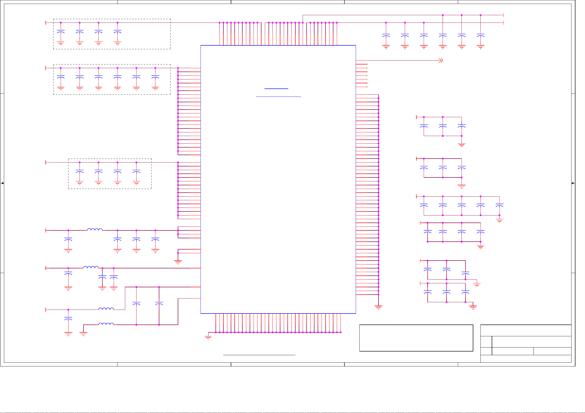
5
+1.2V
C125
0.1uF
D D
+3.3V
C C
+2.5V
B B
A A
+3.3V
+3.3V
+1.2V
* Locate under ZR391055
C145
0.1uF
* Locate under ZR391055
* Locate under ZR391055
C184
1.0uF
C194
1.0uF
C213
1.0uF
5
C126
0.1uF
C146
0.1uF
C170
0.1uF
L21
EXC-CL3225U
L22 EXC-CL3225U
C195
33uF/16V
C127
0.1uF
C147
0.1uF
C171
0.1uF
+
L23
EXC-CL3225U
L24
EXC-CL3225U
C128
0.1uF
C148
0.1uF
C172
0.1uF
+
C183
33uF/16V
P11305CT-ND
C203
0.1uF
C149
0.1uF
C173
0.1uF
C185
0.1uF
C211
0.01uF
* Locate under ZR391055
C150
0.1uF
C186
0.1uF
C212
0.1uF
4
W7
Y7
Y8
AA8
AA9
AA10
K6
J6
H6
H7
G7
G8
F8
F9
F10
CVDD
CVDD
CVDD
CVDD
CVDD
CVDD
CVDD
CVDD
CVDD
CVDD
CVDD
CVDD
CVDD
CVDD
E14
IVDD
E15
IVDD
E16
IVDD
F16
IVDD
AA16
IVDD
AB16
AB15
AB14
AB13
AB12
AB11
AA11
T6
T5
R5
P5
N5
M5
L5
L6
F11
E11
E12
E13
H21
J21
K21
L21
T21
U21
V21
W21
K22
L22
M22
N22
P22
R22
T22
U22
A14
B12
C11
E10
B13
A10
B14
E17
D17
IVDD
IVDD
IVDD
IVDD
IVDD
IVDD
IVDD
IVDD
IVDD
IVDD
IVDD
IVDD
IVDD
IVDD
IVDD
IVDD
IVDD
IVDD
IVDD
MVDD
MVDD
MVDD
MVDD
MVDD
MVDD
MVDD
MVDD
MVDD
MVDD
MVDD
MVDD
MVDD
MVDD
MVDD
MVDD
DACAVDD[1]
DACAVDD[2]
DACAVDD[3]
DACAVDD[4]
DACAVSS[1]
DACAVSS[2]
DHVDD
PLLAVDD
PLLAVSS
GND
V16
GND
V15
GND
V14
GND
V13
GND
V12
GND
V11
GND
U17
GND
U16
GND
U15
GND
U14
ZR391055
POWER & GROUND
GND
GND
GND
GND
GND
T17
T18
U10
U11
U12
U13
Power and Ground 1
4
W6
CVDD
CVDD
GND
GND
T16
U6
V6
CVDD
GND
T14
T15
3
AA20
CVDD
CVDD
GND
GND
T13
3
AA18
AA19
CVDD
GND
T11
T12
AA17
CVDD
CVDD
GND
GND
T10
Y20
CVDD
GND
T9
W20
Y19
CVDD
GND
R17
R18
H20
CVDD
CVDD
GND
GND
R16
G19
G20
CVDD
GND
R14
R15
F20
CVDD
CVDD
GND
GND
R13
F18
F19
CVDD
GND
R11
R12
F17
CVDD
CVDD
GND
GND
R10
U1N
NC7
NC6
NC5
NC4
NC3
NC2
NC1
NC0
GND
GND
GND
GND
GND
GND
GND
GND
GND
GND
GND
GND
GND
GND
GND
GND
GND
GND
GND
GND
GND
GND
GND
GND
GND
GND
GND
GND
GND
GND
GND
GND
GND
GND
GND
GND
GND
GND
GND
GND
GND
GND
GND
GND
GND
GND
GND
GND
GND
GND
GND
GND
GND
GND
GND
ZR391055SH
R9
2
C129
0.1uF
* Locate under ZR391055
A23
AE23
AB19
AB1
W3
Y2
H4
E1
J11
J12
J13
J14
J15
J16
K10
K11
K12
K13
K14
K15
K16
K17
L9
L10
L11
L12
L13
L14
L15
L16
L17
L18
M9
M10
M11
M12
M13
M14
M15
M16
M17
M18
N9
N10
N11
N12
N13
N14
N15
N16
N17
N18
P9
P10
P11
P12
P13
P14
P15
P16
P17
P18
Note: Place 100pf caps within .6" of pin.
Note: Place 1000pf caps within 1.5" of pin.
Note: Place .01uF, .1uF, and 1uF caps within 2" of pin.
C130
0.1uF
+1.2V
D1.2V
+2.5V
+2.5V
+3.3V
+3.3V
2
C190
0.1uF
C141
0.01uF
C131
1000pF
C163
100pF
+
C181
33uF/16V
C187
1000pF
C202
0.1uF
C191
0.1uF
LCD_DIMM
C155
0.1uF
C132
1000pF
C164
100pF
C177
0.01uF
C188
1000pF
C204
+
33uF/16V
C192
0.1uF
C159
+
33uF/16V
C133
1000pF
C165
1000pF
C178
0.1uF
+
C193
0.1uF
C174
0.01uF
C179
0.1uF
C197
0.01uF
C205
33uF/16V
Title
Size Document
B
Date:
Drawn by: O. Marinovsky
1
D1.2V
1.2V
C169
1.0uF
Phobos
BOBCAT_D1_Plus.DSN
Sheet
15 22
of
Wednesday, April 13, 2005
1
Rev
D2
79
Page 80

5
U8B
81
Vcc0
Vcc1
Vcc2
Vcc3
Vcc4
Vcc5
Vcc6
Vcc7
SPLLVcc
SPLLVcc
PLLVcc
PLLVcc
LVDSVcc
LVDSVcc
LVDSVcc3V
LVDSVcc3V
LVDSVcc3V
LVDSVcc3V
Vcc3V
Vcc3V
LVDSGND3V
LVDSGND3V
LVDSGND3V
LVDSGND3V
GND_3V
GND_3V
GND_3V
SPLLGND
SPLLGND
SPLLGND
PLLGND
PLLGND
PLLGND
LVDSGND
LVDSGND
82
75
77
96
119
123
125
87
89
92
94
105
109
101
103
107
111
121
127
102
106
110
112
120
126
128
86
88
90
91
93
95
104
108
113
100
118
122
124
99
67
66
65
83
97
19
20
85
70
33
73
74
76
78
79
80
84
LVDS DRIVER
POWER
PD
PWM
VSTAL
HIRQ
VREF
BAL
TST1
TST2
TST3
RES2
RES3
RES4
GND
GND
GND
GND
GND
GND
GND
GND
GND
GND
GND
DS90C2501
D D
+2.5V
+3.3V
C C
B B
+2.5V
LVDSVcc
PLLVcc
+2.5V
+3.3V
Supply Filters/Bypass, LVDS
4
DDR SDRAM
(PWR)
NC1
NC2
NC3
NC4
NC5
NC6
NC7
VREF
K4H561638F-UC(L)/B3
C214
0.1uF
VREF
+2.5V
C216
0.1uF
14
17
19
25
43
50
53
49
DDR SDRAM
(PWR)
NC1
NC2
NC3
NC4
NC5
NC6
NC7
VREF
K4H561638F-UC(L)/B3
C215
0.1uF
VREF
+2.5V
C217
0.1uF
14
17
19
25
43
50
53
49
U3B
VDD1
VDD2
VDD3
VDDQ1
VDDQ2
VDDQ3
VDDQ4
VDDQ5
VSS1
VSS2
VSS3
VSSQ1
VSSQ2
VSSQ3
VSSQ4
VSSQ5
U4B
VDD1
VDD2
VDD3
VDDQ1
VDDQ2
VDDQ3
VDDQ4
VDDQ5
VSS1
VSS2
VSS3
VSSQ1
VSSQ2
VSSQ3
VSSQ4
VSSQ5
3
+2.5V
1
18
33
3
9
15
55
61
34
48
66
6
12
52
58
64
+2.5V
1
18
33
3
9
15
55
61
34
48
66
6
12
52
58
64
1.8V
A3.3V
L60
BLM18AG601
BLM18AG601
2
1.8V
C395
0.01uF
C391
0.01uF
A3.3V
L61
C394
1.0uF
C390
1.0uF
Supply Bypass, Tuner Demodulator
A3.3V 1.8V
C11
+
1.8V
1.8V
10uF
C514
1000pF
C515
0.1uF
Pin 5 Pin 9 Pin 22 Pin 37 Pin 53 Pin 69 Pin 86 Pin 78
C42
1.0uF
C43
1.0uF
C12
1500pF
C516
1000pF
C44
1.0uF
C517
0.1uF
A3.3V
U9B
78
VccCLK
99
AVcc_ADC
5
Vcor
9
Vcor1
22
Vcor2
53
Vcor4
69
Vcor5
75
VccLO
86
Vcc_PLL
87
Vcc_ADC
84
AVdd_PLL
82 83
Vdd_OSC GND
17
Vdd
30
Vdd
46
Vdd
62
Vdd
74
Vcc(A1)
Cascade-2
+
C13
560pF
C518
1000pF
C523
0.1uF
C14
10uF
C519
0.1uF
C524
1000pF
OREN
C520
0.1uF
C525
0.1uF
TEST
GND
GND
GND
GND
GND
GNDVcor3
GND
GND
GND
GND
GND
GND
GND
GND
GND
GND
GND
GND
GND
GND
C521
0.1uF
C526
1000pF
C15
1500pF
1
3
6
7
15
23
33
3537
45
55
60
70
73
76
77
81
85
88
91
92
95
98
C16
560pF
C527
0.1uF
C528
1.0uF
+2.5V
C237
1.0uF
+2.5V
C247
1.0uF
A A
+2.5V
EXC-CL3225U
EXC-CL3225U
C228
0.1uF
L25
L26
C229
0.1uF
+
+
C244
0.1uF
C236
220uF
C246
220uF
C245
0.1uF
C238
0.1uF
C248
0.1uF
PLLVcc
C239
0.1uF
LVDSVcc
C249
0.1uF
C522
0.1uF
Locate between DDR chips.
Vref = 1.5V
VREF
+2.5V
R205
2K
1
R206
2K
TP3
Supply Bypass, DDR S0
+2.5V
C218
1.0uF
+2.5V
C230
1.0uF
C219
1.0uF
C231
1.0uF
C220
1.0uF
C232
1.0uF
C221
0.1uF
C233
0.1uF
C222
0.1uF
C234
0.1uF
C223
0.1uF
C235
0.1uF
Pin 9 Pin 53 Pin 78
Power and Ground 2
5
4
3
2
Pin 17 Pin 30 Pin 46 Pin 62 Pin 74
Title
Phobos
Size Document
B
BOBCAT_D1_Plus.DSN
Sheet
16 22
of
Wednesday, April 13, 2005
Date:
Drawn by: O. Marinovsky
1
Rev
D2
80
Page 81

5
4
3
2
1
C529
C532
0.1uF
0.1uF
+1.8V
D D
U7E
C533
0.1uF
C534
1000pF
ADV7400
(Power)
C531
0.1uF
6
18
12
39
90
63
47
48
ADV7400A
DVDDIO1
DVDDIO2
DVDD1
DVDD2
DVDD3
AVDD1
PVDD1
PVDD2
NC
DGND1
DGND2
DGND3
DGND4
DGND5
AGND1
AGND2
AGND3
AGND4
ANND5
AGND6
59
5
11
17
40
89
49
50
51
60
66
70
A3.3V
A3.3V
C530
0.1uF
DEC_DVcc
DEC_AVcc
C C
DEC_PVcc
+1.8V
A3.3V
C543
0.1uF
A3.3V
+3.3V_HDMI
L65
MLF2012A4R7K
C537
33uF/16V
L71 MLF2012A4R7K
L64
MLF2012A4R7K
C544
0.01uF
C538
C539
0.1uF
C540
1000pF
0.1uF
+
C535
1000pF
C541
1000pF
C536
1000pF
U10B
82
AUDVcc
66
DVcc
12
CVcc1
24
CVcc2
36
CVcc3
45
CVcc4
81
CVcc5
112
CVcc6
125
CVcc7
87
RVcc
86
XVcc
7
IOVcc1
19
IOVcc2
31
IOVcc3
68
IOVcc4
77
IOVcc5
98
IOVcc6
107
IOVcc7
120
IOVcc8
53
AVcc
57
AVcc
61
AVcc
47 46
PVcc PGND
SiI9011CLU
NC
RSVD
RSVDL
CGND
CGND
CGND
CGND
CGND
CGND
AUDGND
DGND
IOGND
IOGND
IOGND
IOGND
IOGND
IOGND
IOGND
IOGNDAVcc
AGND
AGND
AGND
AGND
43
48
88
13
25
37
80
113
126
83
65
6
18
30
69
78
97
106
11849
52
56
60
64
Supply Bypass, Decoder
L6
EXC-CL3225U
+1.8V
+
+
+
C71
10uF
C76
10uF
C79
10uF
C73
0.1uF
C78
0.1uF
C81
0.1uF
C74
0.1uF
DEC_PVcc
C82
0.1uF
C72
0.1uF
B B
A3.3V
+1.8V
A A
L7
EXC-CL3225U
C77
0.1uF
L8
EXC-CL3225U
C80
0.1uF
DEC_DVcc
C75
0.1uF
DEC_AVcc
DEC_PVcc
Supply Bypass, HDMI Receiver
A3.3V
L66
MLF2012A4R7K
A3.3V
C653
10uF
+
C549
10uF
C654
0.1uF
C550
0.1uF
+
C656
0.1uF
For IOVcc
C551
0.1uF
C657
0.1uF
C552
0.1uF
C658
1000pF
C553
0.1uF
C659
1000pF
C554
1000pF
C660
1000pF
C555
1000pF
+1.8V
C556
1000pF
C666
10uF
C558
1000pF
+
C557
1000pF
C668
C667
0.1uF
0.1uF
For CVcc
C559
1000pF
C669
0.1uF
C560
1000pF
C671
1000pF
C561
1000pF
C672
1000pF
+3.3V_HDMI
C673
1000pF
Title
Phobos
Size Document
B
Power & Ground 3
5
4
3
2
BOBCAT_D1_Plus.DSN
Sheet
17 22
of
Wednesday, April 13, 2005
Date:
Drawn by: O. Marinovsky
1
Rev
D2
81
Page 82

5
4
3
2
1
AP1122 1A 1.2V
LDO
D3.3V +1.2V
L721
D D
FB-3A:TI321611U121
加大散热面积和过孔散热
3.3V
TO-263
U706
AP1122
3
VI
GNDVOTAB
124
L719
FB-3A:TI321611U121
(1.0A)
D6V 5V
U709
3
VI
AP1084K50A
GNDVOTAB
L707
FB-3A:TI321611U121
TO-263
124
D3.3V D1.2V
L723
FB-3A:TI321611U121
C C
D3.3V
L725
FB-3A:TI321611U121
B B
D5V
3.3V
TO-263
3.3V
TO-263
U703
AP1084-3.3
3
VI
3
3
GNDVOTAB
U704
AP1122
VI
U710
AP1122
VI
GNDVOTAB
124
GNDVOTAB
124
L714
FB-3A:TI321611U121
L724
FB-3A:TI321611U121
E713
470uF/16V
L726
FB-3A:TI321611U121
E712
470uF/16V
+3.3V
(1.0A)
+
C719
0.1uF
D6V
TO-263
1.2V
(1.0A)
+
C716
0.1uF
FB-3A:TI321611U121
C703
0.1uF
3
L702
U702
AP1084K50A
VI
124
E711
100uF/16V
GNDVOTAB
+12V
R708 820
3
VI
L704
FB-3A:TI321611U121
U701
AP1084-ADJ
GNDVOTAB
124
R709 150
TO-252
+5VD5V
(2.0A)
L705
FB-3A:TI321611U121
D8VD12V
(1.0A)
T0-263
124
D6V
U711
AP1084-3.3
3
VI
A A
5
GNDVOTAB
124
L717
FB-3A:TI321611U121
E702
100uF/16V
A3.3V
1.2V - 2A (2.8A MAX)
D5V
R713 150
3
TO-252
U705
AP1084-ADJ
VI
GNDVOTAB
124
R712 150
L718
FB-3A:TI321611U121
C717
0.1uF
E718
100uF/16V
+2.5V
2.5V - 1.6A (2.6A MAX)
3.3V - 1.5A (2.3A MAX)
5.0V - 0.5A (1A MAX)
Title
Phobos
Size Document
B
Power & Ground 4
4
3
2
BOBCAT_D1_Plus.DSN
Sheet
18 22
of
Wednesday, April 13, 2005
Date:
Drawn by: O. Marinovsky
1
Rev
D2
82
Page 83

5
4
3
2
1
U708
AP1084K50A_NS
3
D D
VI
GNDVOTAB
124
TO-263
L706
FB-3A:TI321611U121_NS
C718
0.1uF_NS
E717
100uF/16V_NS
(1.0A)
CN701
33P3278 9
1
2
3
4
5
6
7
8
9
9VSC
C707
0.1uF
5VSC
C701
0.1uF
L716
FB-3A:TI321611U121_NS
L712
FB-3A:TI321611U121_NS
9V
D5V
U707
AP1084-5_NS
3
VI
GNDVOTAB
124
L720
FB-3A:TI321611U121_NS
E715
0.1uF_NS
FROM LG PDP
1.8V Linear Regulator for Oren
PSU
+3.3V
C C
3
U208
AZ1117-1.8
VI
GNDVOTAB
124
1.8V
C651
0.1uF
12
C652
47uF/16V
CN702
7
6
5
4
3
2
1
33P3278 7
VS-ONVS-ONVS-ONVS-ONVS-ONVS-ONVS-ONVS-ONVS-ONVS-ONVS-ONVS-ON
STB5VSTB5VSTB5VSTB5VSTB5VSTB5VSTB5VSTB5V
VS-ON
REL-SWRELAY-SW
R131 0_NS
R132 0
STB5V
C705
0.1uF
CN705
12
11
10
9
8
7
6
5
4
3
2
1
33P3278 12
D12V
5VSC
0.1uF
C156
FROM LG PDP
+1.8V Linear Regulator
+3.3V +1.8V
B B
3
VI
U207
AZ1117-1.8
GNDVOTAB
124
C323
0.1uF
12
C324
47uF/16V
PSU
CN706
REL-SW
+5VSB
33P3278 4
4
3
2
1
STB PDC POWER CON
+5VSB
PWR-ON
R125
3.3K
R126
3.3K
+5VSB
Q4
SST3904 BCE
R127
3.3K
+5VSB
R128
3.3K
+5V
NO
USE
REL-SWREL-SW
Q5
SST3904 BCE
E716
100uF/16V_NS
CN703
1
2
3
4
5
6
7
8
9
10
11
33P3278 11
STB5V
1
2
3
4
5
6
7
8
9
10
11
RELAY-SW
D3.3V
FROM SDI PDP
SMPS
CN704
5
5
4
4
3
3
2
2
1
1
33P3278 5
C158
0.1uF
PAD1
Gnd_Mount_Pad
1
1
L722
FB-3A:TI321611U121
L713
FB-3A:TI321611U121_NS
D6V
C706
0.1uF
FB-3A:TI321611U121
C704
C702
0.1uF
0.1uF
L701
L703 FB-3A:TI321611U121
PAD2
Gnd_Mount_Pad
1
1
STB5V
E708
100uF/16V
5VSB+5VD8V
+5VSB
D12V
C157
0.1uF
D6VD12V
POWER TEST POINTS
TP1
+2.5V
+1.2V +12V
A A
1
1
TP7
1
TP12
1
+3.3V +1.8V
TP15
TP13
1
TP4
1
TP8
1
+5V
TP14
1
1
1
1
TP19
TP6
TP9
1
+1.5V
TP16
TP11
1
TP17
1
TP18
1
PAD3
Gnd_Mount_Pad
1
1
Grounded Mounting Holes, PCB
Title
PAD4
Gnd_Mount_Pad
1
1
Phobos
Power & Ground 5
5
4
3
2
83
Size Document
B
BOBCAT_D1_Plus.DSN
Sheet
19 22
of
Wednesday, April 13, 2005
Date:
Drawn by: O. Marinovsky
1
Rev
D2
Page 84

5
4
VCCAUVCCAD V8AUD
3
AGNDC
C661
0.1uF
12
C227
47uF/16V
2
1
U223
D D
I2CCLK0
I2CDATA0
HW_RST_n
RESETn
AUDIO-R
AUDIO-L
C C
B B
AV-IN-R
AV-IN-L
SIF
I2CCLK0
I2CDATA0
R65 0_NS
RESETn
AUDIO-R
AUDIO-L
AV-IN-R
SIF
Y203
18.432MHz
C2028
56pF
1 2
C2039
18pF
C2033 0.33uF
C2034 0.33uF
C2035 0.33uF
C2036 0.33uF
C2037 0.33uF
C2038 0.33uF
12
C2040
18pF
C226
47uF/16V
R63 100
R64 100
C676 0.33uF
C677 0.33uF
C2029 56pF
V8AUD
C655
0.1uF
SC1R
SC1L
SC2R
SC2LAV-IN-L
SC3R
SC3L
SC4R
SC4L
ANI1
ANIM
AXTALI
AXTALO
AVREF
1 2
C224 10uF/16V
1 2
C225 10uF/16V
CPM
CPA
1
2
3
4
5
6
12
7
8
9
62
16
53
63
45
44
43
42
41
40
39
38
37
36
35
47
50
52
51
54
55
46
32
30
SCL
SDA
I2S_CL
I2S_WS
I2S_DO
I2S_DI1
I2S_DI2
ADR_DA
ADR_WS
ADR_CL
ADR_SEL
RESETn
TESTEN
STDBYn
SCI_IR
SCI_IL
ASG1
SC2_IR
SC2_IL
ASG2
SC3_IR
SC3_IL
ASG3
SC4_IR
SC4_IL
MONO_IN
ANA_IN1p
ANA_IN2p
ANA_INm
XTALI
XTALO
VREFTOP
CAPL_M
CAPL_A
10
MSP3455G-QI-B8-V3
11
31
DVSUP1
DVSS
48
49
AHVSUP
AVSS1
33
AVSUP
AHVSS1
34
AGNDC
DACM_R
DACM_L
DACM_SUB
DACA_R
DACA_L
SC1_OR
SC1_OL
SC2_OR
SC2_OL
AUD_CLO
DCTR_IO1
DCTR_IO2
VREF1
VREF2
27
19
NC1
NC2
NC3
NC4
NC5
NC6
NC7
NC8
TP
56P 593 2
20
21
23
17
18
28
29
25
26
57
60
61
13
14
15
22
24
58
59
64
56
AUDMR
AUDMLAUDML
AUDAR
AUDAL
C2043
1nF_NS
C2044
1nF_NS
SC-R1
SC-L1
E226 1uF/16V
E231 1uF/16V
C240
47uF/16V
1 2
1 2
12
V8AUDV8AUD
C663
470pF
1 2
C2045
1nF_NS
5VSB 5VSB
C2046
1nF_NS
D8V
L216
FB_1K_OHM_200MA
E227 1uF/16V
E232 1uF/16V
1 2
L218
10UH
EARPHONE_R
EARPHONE_L
AV-R
AV-L
C664
0.1uF
L217
FB_1K_OHM_200MA
AUDMR
AUDML
EARPHONE_R
EARPHONE_L
AV-R
AV-L
VCCADVCCAU
FQFP-64
I2C: 0x80
A A
C665
470pF
C670
0.1uF
12
C241
47uF/16V
C674
470pF
C675
0.1uF
Title
12
C242
47uF/16V
Phobos
Size Document
B
BOBCAT_D1_Plus.DSN
Sheet
20 22
of
Wednesday, April 13, 2005
Date:
5
4
3
2
Drawn by: O. Marinovsky
1
84
Rev
D2
Page 85

5
J603
D D
1
2
3
4
5
6
33P3278 6
12V-AUDIO
0.1uF
C696
L634 33uH/2A
1 2
12
0.1uF
C697
12VAMP
+
E632
1000uF/16V
4
R189
EARPHONE_R
EARPHONE_L
EARPHONE_R
EARPHONE_L
3.3K
R214
3.3K
3
E222
12
1uF/16V
E225
12
1uF/16V
R647 10K
R646 10K
R649 10K
R648 10K
3
2
12VAMP
5
6
84
+
-
84
+
-
2
U602A
1
TL072CD
10K_NS
U602B
7
TL072CD
R651
R650
10K
E224 1uF/16V
1 2
1 2
E223 1uF/16V
R652
10K
D3.3V
R654 10K_NS
PHONE-ON
EAR_R
EAR_L
C714
100pF
C715
100pF
1
J11
5
5
4
4
3
3
2
2
1
1
33P3278 5
TO Earphone OUTPUT
J605
1
2
3
C C
B B
A A
4
33P3278 4_NS
470uF/16V_NS
AUD_DOWN
E1
AUD_DOWN
24V
+
AUDML
AUDMR
U12
1
Vin
ON/OFF
C166
0.1uF_NS
R301 10K
AUD_DOWN
5
LM2596T-12_NS
AUDML
AUDMR
AUD_DOWN
Feedback
Vout
GND
3
1N5822_NS
R636 3.3K
4
2
D12
STB5V
E630
2.2uF/16V
E631
2.2uF/16V
STB5V
R635
3.3K
12V-AUDIO
C695
0.1uF_NS
R642 20K
+
R644 20K
+
R637 3.3K
Q631
SST3904 BCE
C631
1.0uF
R638
1K
Q630
SST3904 BCE
C698
0.1uF
R641 8.2K
R643 20K
R645 20K
C632
0.1uF
MUTEMUTE
U601
1
+5GEN
2
DCAP1
3
DCAP2
4
V5D
5
AGND1
6
REF
7
OVERLOAD
8
AGND2
9
V5A
10
VP1
11
IN1
12
MUTE
13
NC
14
VP2
15
IN2
16
BIASCAP
17
AGND3
18 19
SLEEP FAULT
CPUMP
PGND1
NC
VDDA
NC
OUTP1
VDD1
VDD1
OUTM1
OUTM2
VDD2
VDD2
OUTP2
NC
DGND
NC
PGND2
TA2024
PHONE-ON
R655
1K
TA2024 OUTPUT GND AND INPUT GND
NEED TO BE CONNECTED BY ONE POINT.
C700 1.0uF
36
35
34
33
32
31
30
29
28
27
26
25
24
23
22
21
20
C699
0.1uF
12VAMP
12VAMP
(1) C634,C647,C649 NEAR TO THE PINS OF VDD AND PGND
12VAMP
C708
0.1uF
(3) L630~L633 FAR TO THE PINS OF OUTPUT
L630 10uH/3A
1 2
12
D630 MBRS130T3
L631 10uH/3A
1 2
12
D631 MBRS130T3
D632 MBRS130T3
L632 10uH/3A
1 2
12
D633 MB RS130T3
L633 10uH/3A
1 2
12
12
12
12
(2) D630~D633 NEAR TO THE PINS OF OUTPUT AND PGND
C709
1000pF
12
LOUT+
LOUT-
ROUT-
C641
0.47uF
ROUT+
C710
0.47uF
C711
0.47uF
R639
10 1/4W
C640
0.47uF
C642
0.47uF
R640
10 1/4W
C646
0.47uF
C712
0.1uF
C643
0.1uF
C713
1000pF
C639
1000pF
C644
1000pF
C645
1000pF
R653 10K_NS
L638 FB
1 2
12
L637 FB
1 2
12
L636 FB
1 2
12
L635 FB
1 2
12
LO+
COMLO-
COMRO-
RO+
J14
1
1
2
2
3
3
4
4
5
5
33P3278 5
Title
Phobos
Size Document
B
BOBCAT_D1_Plus.DSN
Sheet
21 22
of
Monday, April 18, 2005
Date:
5
4
3
2
Drawn by: O. Marinovsky
1
85
Rev
D2
Page 86

86
Page 87

5
4
3
2
1
GPIO Pin Table
Signal
ZR391055 GPIO #
Function
Setting
Active high.0 LCD backlight ON/OFF control.LCD_ON
NAND_GPIO1_n 1
D D
Video_Input_Select 2 Composite - Y/C Video Input recognition.
Allow to boot-up from NAND FLASH Active low.
1 = Composite, 0 = Y/C
1 = WR Enable, 0 = protected.3 NAND FLASH WR protectionWP~
CH +
CH VOL +
VOL AUD_DOWN
11
AUD_DOWN MUTE
Active low.4 Tuner control / Setup errow
Active low.5 Tuner control / Setup errow
Active low.6 VOL control / Setup errow
Active low.7 VOL control / Setup errow
(see table p.05)12 AUDIO IN SelectAUD_SEL_A
(see table p.05)13 AUDIO IN SelectAUD_SEL_B
AUD_SEL_C 14 AUD I O I N S e l e ct (see ta b le p . 0 5 )
CVmix_SEL 104
C C
ACLK_SEL0
ACLK_SEL1
FMS_SEL
HD_DOWN
107
108
109
110
HDMI_SCDT 112 HDMI Si gnal Detect Active high.
TV_VIDEO 113 VIDEI O I N S e l e ct / F P S W Active low.
IDE_HSCBL_n
119
Analog video composite summer
Active lowHead Phone MUTE
ACLK select source - HDMI/CLK GEN Active low.
Active low.ACLK select source - HDMI/CLK GEN
RGB out filter select HD/SD
Active low.
FunctionDS90C2501 GPIO#
0 LVDS Control
1
2 DUAL Function
COLOR Function Active low.
Setting
Active high.
AIN_INT_n 120 Ana l o g D e c oder I C In t. Active low.
121 2 COMPONENT SIGNAL SW (see table p.07)HD_SEL
CEC 122 HDMI c o n t r o l
SLEEP_MODE_n
123
Active low.LOW PWR mode control
HDMI_VSYNC 125 SYNC signal control from H DMI s ours e.
B B
154 SPI EEPROM Wright protection. Active low.SPIEEPROM_WP_n
Active high.LAN_INT 155 Ether n e t I C I nt.
HDMI_INT 156 HDMI IC Int.
Active high.
157 Subcarrier Frequency Lock FSC_LOCK
158 LCD P WM Contro l.LCD_PWM
(see table p11)161ACS0 Audio Cl o ck Fr eq . S e l b i t 0 ( M a in )
ACS1
160 Audio Clock Freq. Sel bit 1 (Main)
(see table p11)
(see table p11)162 Audio Clock Freq. Sel bit 2 (Main)ACS2
HD_SYNC_SEL
LED2
LED3
LED4
A A
LED5
LED6 1 = off, 0 = lit
MENU
5
163
159
166
167
168
169
HD_SYNC_SEL
LED D2 Control
LED D3 Control
LED D4 Control
LED D5 Control
LED D6 Control
1 = off, 0 = lit
1 = off, 0 = lit
1 = off, 0 = lit
1 = off, 0 = lit
184 SEL / FP SW Active low.
GPOIs Table
4
3
Title
Phobos
Size Document
B
BOBCAT_D1_Plus.DSN
Sheet
Monday, March 28, 2005
Date:
2
Drawn by: O. Marinovsky
of
22 22
1
Rev
D2
87
Page 88

Spare Parts List
EN 21.
Set Level 42MF130A/37
Various
0001 9965 000 29550 Plasma panel
0002 9965 000 29551 Conductive filter
0003 9965 000 29552 Key board
0004 9965 000 29553 Image board
0005 9965 000 29554 Control stand
0006 9965 000 29555 Power switch board
0007 9965 000 29556 PSPC
0008 9965 000 29557 Front/side AV board
0009 9965 000 29558 Stand assy
0010 9965 000 29562 Front assy
0011 9965 000 29563 Bear-cover-M
0012 9965 000 29564 Bear cover low
0013 9965 000 29565 Bear cover BKT
0014 9965 000 29566 Internal sound box L
0015 9965 000 29567 Internal sound box R
0016 9965 000 29568 Handle
0017 9965 000 29569 Image to panel LVDS
0028 9965 000 29570 Power cord
0030 9965 000 29571 Remote control
0031 9965 000 29572 Manual
Boards Plasma Panel 42MF130A/37
Various
0034 9965 000 30132 Assy PCB buffer(E)
0035 9965 000 30133 Assy PCB buffer(F)
0036 9965 000 30134 Assy PCB buffer(G)
0037 9965 000 30135 Assy PCB buffer(Y-up)
0038 9965 000 30136 Assy PCB buffer(Y-low)
0039 9965 000 30137 Assy PCB logic main
0040 9965 000 30138 Assy PCB Y main
0041 9965 000 30139 SMPS
0042 9965 000 30140 SMPS-video
0043 9965 000 30141 Assy PCB X main
0044 9965 000 30142 Image board
0045 9965 000 30212 Key press 7x
0046 9965 000 30213 2005 lenss
0047 9965 000 30214 Front assy
0048 9965 000 30215 Dust proof sponge
0049 9965 000 30216 Dust proof sponge
0050 9965 000 30217 Conductive fabric/1000*
0051 9965 000 30218 EMI sponge 620x10x4
0059 9965 000 30219 Rear cover M
0060 9965 000 30220 Rear low cover
0074 9965 000 29570 Power cord
0077 9965 000 29571 Remote control
950*10
550*10
Boards Plasma Panel 42MF230A/37
Various
0087h 9965 000 30222 Assy PCB buffer(E)
h 9965 000 30223 Assy PCB buffer(F)
0088
0089
h 9965 000 30224 Assy PCB buffer(Y-up)
h 9965 000 30225 Assy PCB buffer(Y-low)
0090
h 9965 000 30226 Assy PCB logic main
0091
0092
h 9965 000 30227 Assy PCB Y main
h 9965 000 30228 SMPS
0093
h 9965 000 30229 SMPS-video
0094
0095
h 9965 000 30230 Assy PCB X main
h 9965 000 30142 Image board
0096
Set Level 42MF230A/37
Various
0001h 9965 000 30175 Plasma panel
0002 9965 000 29551 Conductive filter
0003 9965 000 29552 Key board
h 9965 000 30176 Image board
0004
0005 9965 000 29554 Control stand
0006 9965 000 30177 PSPC
0007 9965 000 30178 PSPC
0008 9965 000 29557 Front/side AV board
0009 9965 000 30179 Stand assy
0011 9965 000 30180 Logo
0012 9965 000 30181 BKT-main-power
0013 9965 000 30182 Handle
0014 9965 000 30183 PDP Internal sound box L
0015 9965 000 30184 PDP Internal sound box R
0016 9965 000 30185 Corner rubber
0017 9965 000 30186 Al foil
0018 9965 000 30187 Al foil
0019 9965 000 30188 Foam 1000x10x2
0020 9965 000 30189 EMC Foam
0021 9965 000 30190 EMC Foam
0022 9965 000 30191 EMI sponge 110x10x2
0023 9965 000 30192 EMI sponge 110x10x6
0024 9965 000 30193 EMC Foam 90*W10*T8
0025 9965 000 30194 EMI sponge 80x10x2
0026 9965 000 30195 EMI sponge
0029 9965 000 30196 EMI core
0030 9965 000 30197 EMI filter
0031 9965 000 30198 Wire harness
0032 9965 000 30199 Wire
0033 9965 000 30200 Wire harness
0034 9965 000 30201 Wire harness
0035 9965 000 30202 Wire harness
0036 9965 000 30203 Wire harness
0037 9965 000 30204 Wire harness
0038 9965 000 30205 Wire harness
0039 9965 000 30206 Wire harness
0040 9965 000 30207 Wire harness
0041 9965 000 30208 Shield-1
0042 9965 000 30209 BKT-shield52
0043 9965 000 30210 BKT-holder-5
0044 9965 000 30211 Front bottom
88
Page 89

REVISION LIST
3122 785 1569
0
First Release
3122 785 156
91 Model 42MF230A/37 added, 42MFx30A/37 as mentioned in this manual,
means both 42MF130A/37 and 42MF230A/37 sets.
THESE DOCUMENTS ARE FOR REPAIR SERVICE INFORMATION ONLY. EVERY REASONABLE
RT HAS BEEN MADE TO ENSURE THE ACCURACY OF THIS MANUAL; WE CANNOT
EFFO
GUARANTEE
DISCLAIMS
THE ACCURACY OF THIS INFORMATION AFTER THE DATE OF PUBLICATION AND
RELIABILITY FOR CHANGES, ERRORS OR OMISSIONS.
89
 Loading...