


Service Manual
Service
Service
Micro System
Service
Service
Service
MCM8/21/22/25
©
Copyright 2004 Philips Consumer Electronics B.V. Eindhoven, The Netherlands
All rights reserved. No part of this publication may be reproduced, stored in a retrieval system or
transmitted, in any form or by any means, electronic, mechanical, photocopying, or otherwise
without the prior permission of Philips.
Published by BB 0412 Service Audio Printed in The Netherlands Subject to modification
Version 1.1
TABLE OF CONTENTS
Page
Location of pc boards & Version variations................1-2
Technical Specifications ............................................. 1-3
Measurement setup ....................................................1-4
Service Aids, Safety Instruction, etc...........................1-5
Disassembly Instructions & Service positions .............. 2
Service Test Program .................................................3-1
Set Block diagram ......................................................4-1
Set Wiring diagram .....................................................5-1
Front Board .................................................................... 6
ECO6 Tuner Board : Systems Non-Cenelec............. 7A
Systems Cenelec..................... 7B
ETF8 Tape Module ........................................................ 9
Universal Loader ......................................................... 10
Power 2003 Module (75-150W Class D)..................... 11
Set Mechanical Exploded view & parts list ................. 12
Revision List ................................................................ 13
CLASS 1
LASER PRODUCT
GB
3139 785 30621
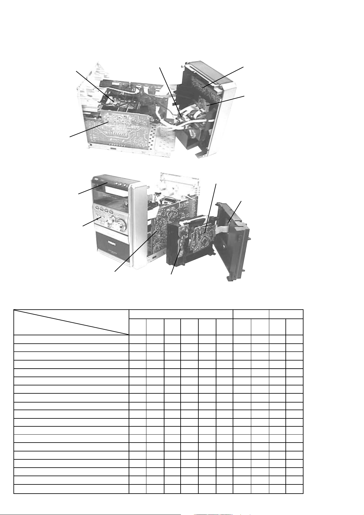
LOCATION OF PC BOARDS
1-2
Tuner Board
Mains Board
Top Key Board
Control Board
ETF8 SD Board
Display Board
Eeprom Board
CD Board
MP3 CD03 Board
Combi Board
VERSION VARIATIONS:
Type /Versions: MCM8
Features &
Board in used:
Aux in / CDR in x x x
Line Out
Video Out
Surround Out
Subwoofer Out
Digital Out
Digital in
Matrix Surround
RDS/NEWS x x
Dolby Pro Logic (DPL)
Incredible Surround x x x
Karaoke Features
Voltage Selector x
ECO Power Standby (Clock Display Off) x x x
ECO6 Tuner Board - Systems Non-Cenelec x
ECO6 Tuner Board - Systems Cenelec x x
Tray Motor Board
/21 /22 /25

SPECIFICATIONS
1-3
GENERAL:
Mains voltage : 110-127V/220-240V Switchable for /21/21M
120V for /37
220V for /33
220-230V for /22/25
230-240V for /30
Mains frequency : 50/60Hz
Power consumption : 60W at 1/8 P
65W at 1/8 P
rated
rated
/21/21M
< 15W at Standby (Demo mode off)
< 0.5W at ECO Standby
< 1.0W at ECO Standby /21/21M
Clock accuracy : < 4 seconds per day
Dimension centre unit : 175 x 252 x 350mm
TUNER:
FM
Tuning range : 87.5-108MHz
Grid : 50kHz
100kHz for /37
IF frequency : 10.7MHz ± 25kHz
Aerial input : 75 ohm coaxial
300 ohm click fit for /37
Sensitivity at 26dB S/N : < 7uV
Selectivity at 600kHz bandwidth : > 25dB
Image rejection : > 25dB [> 75dB]
Distortion at RF=1mV, dev. 75kHz : < 3%
-3dB Limiting point : < 8uV
Crosstalk at RF=1mV, dev. 40kHz : > 18dB
Input sensitivity
Aux in (at 1kHz) : 500mV at 600 ohm
CDR in (at 1kHz) : 1000mV at 600 ohm
Output sensitivity
Headphone output at 32 ohm : 15mW ± 2dB (Max. vol.)
CD Headphone output at 32 ohm : 5mW ± 2dB (Max. vol.)
CASSETTE RECORDER:
Number of track : 2 tracks (stereo)
Tape speed : 4.76 cm/sec ± 2%
Wow and flutter : < 0.4% DIN
Fast-wind/Rewind time C60 : 130 sec
Bias system : 78kHz ± 10kHz
Rec/Pb frequency response within 8dB: 80Hz - 10kHz
Signal to Noise Ratio (Type I) : > 48dBA
Signal to Noise Ratio (Type II) : > 52dBA
COMPACT DISC:
Measurement done directly at the connector on the board.
Output Resistance : < 100 ohm
Output Voltage (0dB, 1kHz) : 0.5Vrms ± 1dB (unloaded)
Channel Unbalance : < ±1dB
Channel Separation (1kHz) : > 60dB
Frequency Response (±3dB) : 20Hz-20kHz
Signal to Noise Ratio : > 76dBA
MP3-CD Bit Rate : 32-256 kbps
Sampling Frequencies : 32, 44.1, 48 kHz
MW
Tuning range : 531-1602kHz
530-1700kHz for /21/21M/37
Grid : 9kHz
10kHz for /21/21M/37
IF frequency : 450kHz ± 1kHz
Aerial input : Frame aerial
Sensitivity at 26dB S/N : < 4.4mV/M
Selectivity at 18kHz bandwidth : > 18dB
IF rejection : > 45dB
Image rejection : > 28dB
Distortion at RF=50mV, M=80% : < 5%
AMPLIFIER:
Output power (6 ohm, 1kHz, 10% THD)
L & R : 2 x 75W RMS
Frequency response within -3dB : 50Hz-16kHz
Bass : 60Hz ± 3 Steps
Treble : 12kHz ± 3 Steps
Incredible Surround : On / Off
[....] Values indicated are for "ECO6 Cenelec Board" only.
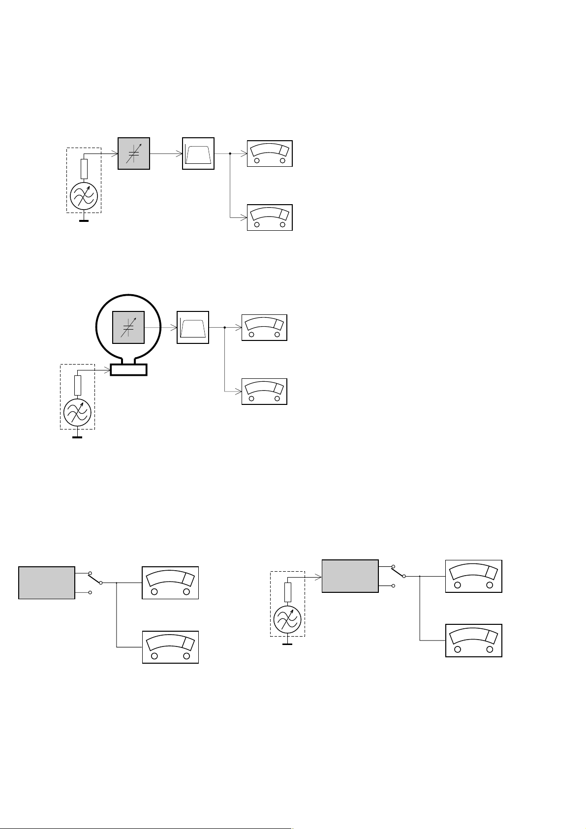
MEASUREMENT SETUP
Tuner FM
1-4
Bandpass
LF Voltmeter
e.g. PM2534
RF Generator
e.g. PM5326
DUT
250Hz-15kHz
e.g. 7122 707 48001
Ri=50Ω
S/N and distortion meter
e.g. Sound Technology ST1700B
Use a bandpass filter to eliminate hum (50Hz, 100Hz) and disturbance from the pilottone (19kHz, 38kHz).
Tuner AM (MW,LW)
RF Generator
e.g. PM5326
Ri=50Ω
DUT
Frame aerial
e.g. 7122 707 89001
Bandpass
250Hz-15kHz
e.g. 7122 707 48001
LF Voltmeter
e.g. PM2534
S/N and distortion meter
e.g. Sound Technology ST1700B
To avoid atmospheric interference all AM-measurements have to be carried out in a Faraday´s cage.
Use a bandpass filter (or at least a high pass filter with 250Hz) to eliminate hum (50Hz, 100Hz).
CD
Use Audio Signal Disc
(replaces test disc 3)
DUT
L
R
SBC429 4822 397 30184
S/N and distortion meter
e.g. Sound Technology ST1700B
LEVEL METER
e.g. Sennheiser UPM550
with FF-filter
Recorder
Use Universal Test Cassette CrO2 SBC419 4822 397 30069
or Universal Test Cassette
LF Generator
e.g. PM5110
Fe SBC420 4822 397 30071
DUT
L
R
S/N and distortion meter
e.g. Sound Technology ST1700B
LEVEL METER
e.g. Sennheiser UPM550
with FF-filter
SERVICE AIDS
Service Tools:
Universal Torx driver holder .................................. 4822 395 91019
Torx bit T10 150mm ............................................. 4822 395 50456
Torx driver set T6 - T20 ......................................... 4822 395 50145
Torx driver T10 extended ...................................... 4822 395 50423
Compact Disc:
SBC426/426A Test disc 5 + 5A ............................ 4822 397 30096
SBC442 Audio Burn-in Test disc 1kHz ................. 4822 397 30155
SBC429 Audio Signals disc .................................. 4822 397 30184
Dolby Pro-logic Test Disc ...................................... 4822 395 10216
1-5
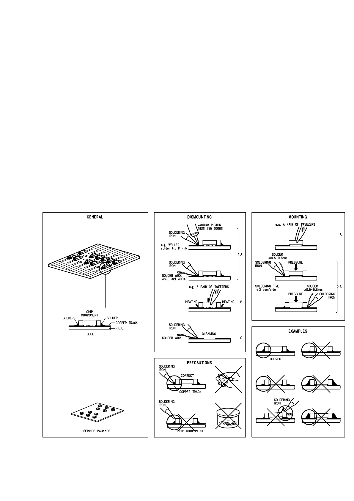
HANDLING CHIP COMPONENTS

1-6
GB
All ICs and many other semi-conductors are
susceptible to electrostatic discharges (ESD).
Careless handling during repair can reduce life
drastically.
When repairing, make sure that you are
connected with the same potential as the mass
of the set via a wrist wrap with resistance.
Keep components and tools also at this
potential.
Tous les IC et beaucoup d’autres
semi-conducteurs sont sensibles aux
décharges statiques (ESD).
Leur longévité pourrait être considérablement
écourtée par le fait qu’aucune précaution n’est
prise à leur manipulation.
Lors de réparations, s’assurer de bien être relié
au même potentiel que la masse de l’appareil et
enfiler le bracelet serti d’une résistance de
sécurité.
Veiller à ce que les composants ainsi que les
outils que l’on utilise soient également à ce
potentiel.
F
WARNING
ATTENTION
GB
Complete Kit ESD3 (small tablemat, wristband,
connection box, extention cable and earth cable) ...........4822 310 10671
Wristband tester ....................................................................4822 344 13999
ESD
D
WARNUNG
Alle ICs und viele andere Halbleiter sind
empfindlich gegenüber elektrostatischen
Entladungen (ESD).
Unsorgfältige Behandlung im Reparaturfall kan
die Lebensdauer drastisch reduzieren.
Veranlassen Sie, dass Sie im Reparaturfall über
ein Pulsarmband mit Widerstand verbunden
sind mit dem gleichen Potential wie die Masse
des Gerätes.
Bauteile und Hilfsmittel auch auf dieses gleiche
Potential halten.
ESD PROTECTION EQUIPMENT:
NL
Alle IC’s en vele andere halfgeleiders zijn
gevoelig voor electrostatische ontladingen (ESD).
Onzorgvuldig behandelen tijdens reparatie kan
de levensduur drastisch doen verminderen.
Zorg ervoor dat u tijdens reparatie via een
polsband met weerstand verbonden bent met
hetzelfde potentiaal als de massa van het
apparaat.
Houd componenten en hulpmiddelen ook op
ditzelfde potentiaal.
Tutti IC e parecchi semi-conduttori sono
sensibili alle scariche statiche (ESD).
La loro longevità potrebbe essere fortemente
ridatta in caso di non osservazione della più
grande cauzione alla loro manipolazione.
Durante le riparazioni occorre quindi essere
collegato allo stesso potenziale che quello della
massa dell’apparecchio tramite un braccialetto
a resistenza.
Assicurarsi che i componenti e anche gli utensili
con quali si lavora siano anche a questo
potenziale.
WAARSCHUWING
I
AVVERTIMENTO
GB
Safety regulations require that the set be restored to its original
condition and that parts which are identical with those specified,
be used
Safety components are marked by the symbol
!
.
NL
Veiligheidsbepalingen vereisen, dat het apparaat bij reparatie in
zijn oorspronkelijke toestand wordt teruggebracht en dat onderdelen,
identiek aan de gespecificeerde, worden toegepast.
De Veiligheidsonderdelen zijn aangeduid met het symbool
!
F
Les normes de sécurité exigent que l’appareil soit remis à l’état
d’origine et que soient utiliséés les piéces de rechange identiques
à celles spécifiées.
Less composants de sécurité sont marqués
!
D
Bei jeder Reparatur sind die geltenden Sicherheitsvorschriften zu
beachten. Der Original zustand des Geräts darf nicht verändert werden;
für Reparaturen sind Original-Ersatzteile zu verwenden.
Sicherheitsbauteile sind durch das Symbol
!
markiert.
I
Le norme di sicurezza esigono che l’apparecchio venga rimesso
nelle condizioni originali e che siano utilizzati i pezzi di ricambio
identici a quelli specificati.
Componenty di sicurezza sono marcati con
!
CLASS 1
LASER PRODUCT
GB
Invisible laser radiation when open.
Avoid direct exposure to beam.
Osynlig laserstrålning när apparaten är öppnad och spärren
är urkopplad. Betrakta ej strålen.
SF
Avatussa laitteessa ja suojalukituksen ohitettaessa olet alttiina
näkymättömälle laserisäteilylle. Älä katso säteeseen!
DK
Usynlig laserstråling ved åbning når sikkerhedsafbrydere er
ude af funktion. Undgå udsaettelse for stråling.
S
Warning !
Varning !
Varoitus !
Advarse !
GB
After servicing and before returning set to customer perform a leakage
current measurement test from all exposed metal parts to earth ground to
assure no shock hazard exist. The leakage current must not exceed
0.5mA.
F
"Pour votre sécurité, ces documents doivent être utilisés par
des spécialistes agréés, seuls habilités à réparer votre
appareil en panne".
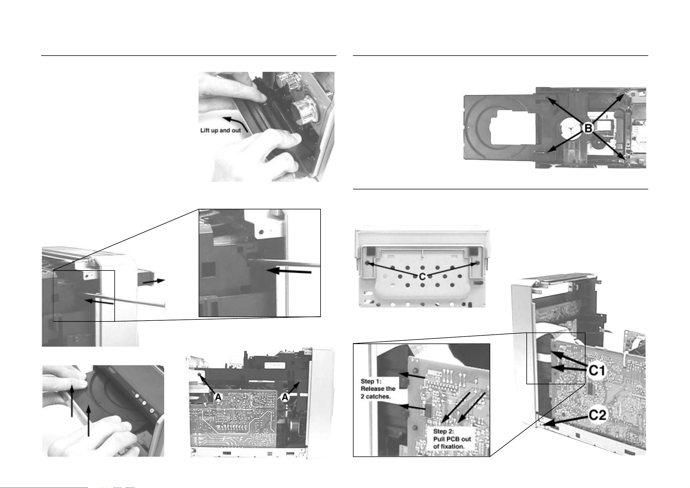
DISMANTLING INSTRUCTIONS
2-1 2-1
Dismantling of the Cover Cassette and Universal Loader
1) Remove the Cover Cassette (pos 150) in the direction as
shown in Figure 1.
2) Loosen 4 screws to remove the Cover Top (pos 240) by
sliding it out towards the rear before lifting up.
- 2 screws on the rear
- 1 screw each on the left & right side
3) Loosen 2 screws each to remove the Panel Left (pos 180)
and Panel Right (pos 181). The Panels are removed by
sliding it towards the rear and outwards.
- 1 screw on the rear
- 1 screw on the side
- see Service position A
4) Use a screw driver to give a push in the direction as shown
in Figure 2 and Figure 2A to unlock the Loader Tray before
sliding it out.
5) Slide out the Loader Tray and remove the Cover CD (pos
110 + pos 111) in the direction as shown in Figure 3.
6) Loosen 4 screws A (see Figure 4) to remove the Bracket
Module Mounting (pos 156) and Universal Loader (pos
1103).
- 2 screws each on the left & right side
Figure 1
Detaching the Universal Loader from the Bracket Module Mounting
1) Slide out the Loader Tray fully and remove 4 screws B (see
Figure 5) to detach the Universal Loader (pos 1103) from
the Bracket Module Mounting (pos 156).
- see Service position B
Figure 5
Detaching the Front Panel assembly from the Bottom/Rear assembly
1) Remove 2 screws C (see Figure 6) from the bottom of the
Cabinet Front (pos 101).
2) Release the fixation of the Combi Board (pos1102-1001)
to Bracket Combi (pos 155) by releasing the 2 catches C1
(see Figure 7) and pulling the Combi Board outwards as
shown in Figure 7A.
3) Uncatch 2 catches C2 (see Figure 7) on the left & right
sides of the Cabinet Front (pos 101) and slides the Front
Panel assembly out towards the front.
- see Service position C
Figure 2
Figure 3
Figure 2A
Figure 4
Figure 6
Figure 7A Figure 7
DISMANTLING INSTRUCTIONS
2-2
2-2
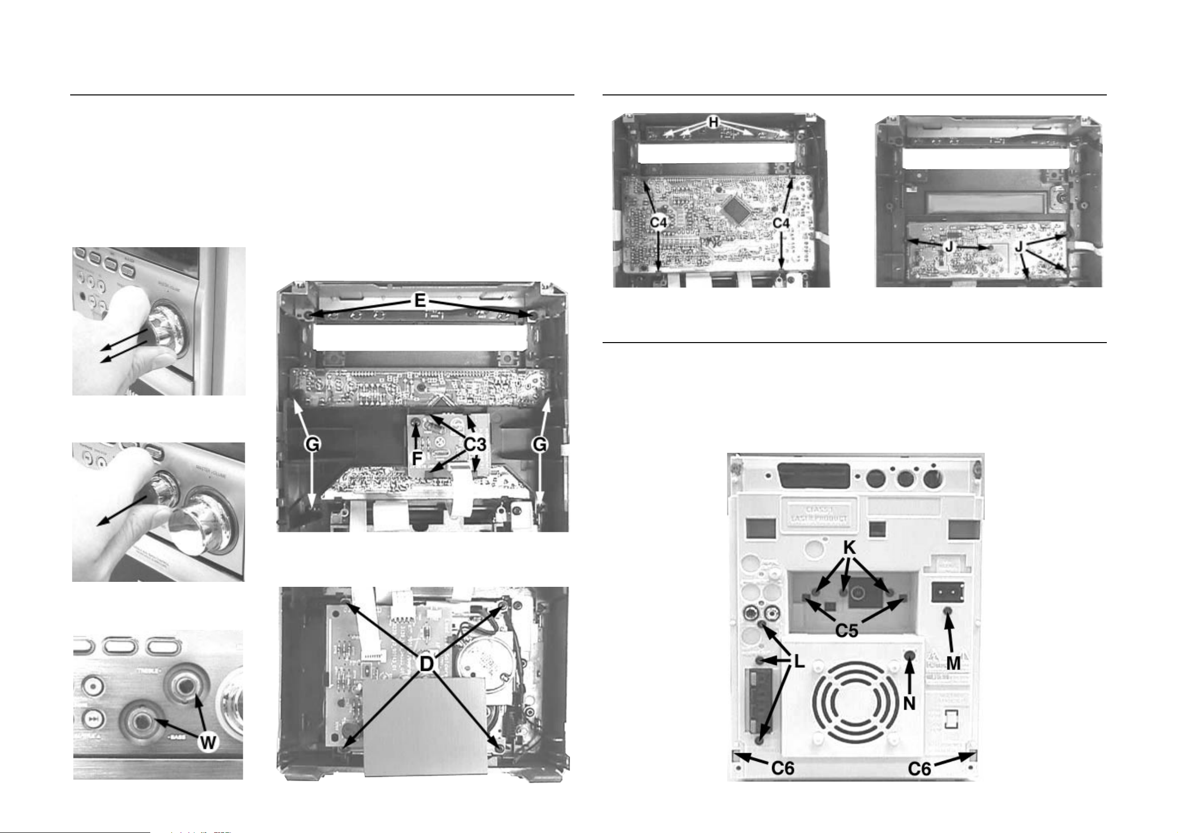
Dismantling of the Front Panel assembly
1) The Knob Volume (pos 141) can be remove by pulling it
out in the direction as shown in Figure 8.
2) The Knob Bass/Knob Treble (pos 140) can be remove by
pulling it out in the direction as shown in Figure 9.
3) Loosen 4 screws D (see Figure 12) to remove the Shield
Tape Deck and Module Tape Deck (pos 1107).
4) Loosen 2 screws E (see Figure 11) to remove the Bracket
Top Support (pos 113).
Figure 8
5) Loosen 1 screw F and 4 catches C3 (see Figure 11) to
remove the Eeprom Board (pos 1105D).
6) Loosen 4 screws G (see Figure 11) to remove the Bracket
Combi (pos 155).
7) Uncatch 4 catches C4 (see Figure 13) to remove the
Display Board (pos 1105A)
8) Loosen 4 screws H (see Figure 13) to remove the Top
Key Board (pos 1105C).
9) Loosen 5 screws J (see Figure 14) and 2 nuts W (see
Figure 10) to remove the Control Board (pos 1105B).
Dismantling of the Front Panel assembly
Figure 13
Dismantling of the Rear Panel assembly
1) Loosen 3 screws K and 2 catches C5 (see Figure 15) to
remove the Tuner Board assembly.
2) Loosen 3 screws L (see Figure 15) to free the Combi
Board (pos 1102-1001).
3) Loosen 1 screw M (see Figure 15) to free the Mains
Socket Board (pos 1102-1002B).
Figure 14
4) Loosen 1 scew N and 2 catches C6 (see Figure 15) to
free the Panel Rear (pos 230) by sliding it out towards the
rear.
Note : Tuner Board assembly and Mains Socket Board
can also be remove together with the Panel Rear.
Figure 9
Figure 10
Figure 11
Figure 12 Figure 15
DISMANTLING INSTRUCTIONS
2-3 2-3
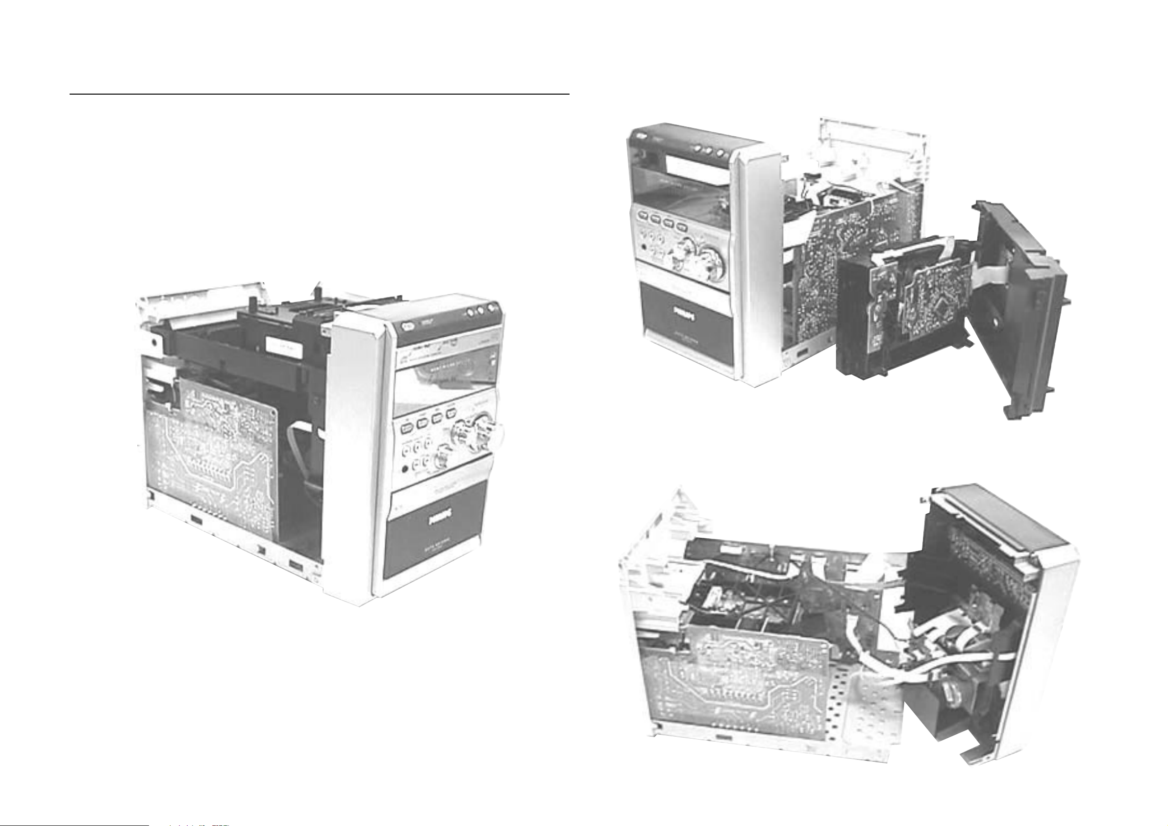
Repair Hints & Service Positions
1) During repair it is possible to disconnect the Tuner Board
and/or CD Module completely unless the fault is suspected to be in that area. This will not affect the
performance of the rest of the set.
Service position A
Service position B
Note: The flex cables are very fragile, care should be taken
not to damage them during repair. After repair, be
very sure that the flex cables are inserted properly
into the flex sockets before encasing, otherwise faults
may occurs.
Service position C
SERVICE TEST PROGRAM
3-1
To start service test program
plugging in the mains cord
S
hold & ECO
depressed while
3-1
TUNER
TEST
TUNER
Button pressed?
Y
Display Tuner Version
"ccc"
TUNER
Button pressed?
Y
Service frequencies are
copied to the RAM (see Table 1)
Tuner works normally except:
PROGRAM button
Disconnect
Mains cord ?
Y
Service Mode left
Display shows the
ROM version
"S-Vyy"
(Main menu)
QUARTZ
TEST
N
N
N
TAPE
Button pressed?
Y
Display shows
32K
Output at (Display Board)
pin 19 of uP = 2048Hz
TAPE
Button pressed?
Y
Display shows
12M
Output at (Display Board)
pin 19 of uP = 2,929.6875Hz
9
Button pressed?
Y
N
CD (on RC)
Button pressed?
Y
Note : Disc should be available on the tray before entering the Service Test Mode.
STEP
DISPLAY
MP3CD’03
N
Choose
level
by pressing
on the RC
Q
N
R
1
TI-Vnn
2
TI BUS
3
SLD I
4
SLD O
5
TI FOC
6
MP3-CD MODULE
TEST
N
MESSAGE
OKAY
-
-
BUS OK
-
-
FOC OK
ERROR
-
-
BUS ER
-
-
FOC ER
ACTION
Indicates the module used.
Version of the MPEG software (nn = Version Number).
Communication test between the Main uP and CD Module.
CD SLEDGE MOTOR is moved in.
CD SLEDGE MOTOR is moved out.
FOCUS SERVO Test.
Press
S refers to Service Mode
V refers to Version
yy refers to Software version number of the uProcessor
(counting up from 01 to 99)
9
to exit.
DISPLAY
TEST
DIM or RDS
Button pressed?
Y
Display shows Figure 1
and switch all LEDs on
except ECO LED
(see Table 2 Pattern 1)
DIM or RDS
Button pressed?
Y
Display shows Figure 2
and switch alternate LEDs on
(see Table 2 Pattern 2)
9
Button pressed?
Y
ADC
TEST
N
N
N
AUX
Button pressed?
Y
Display shows "ADC1 Value"
for ADC1
(Input Line - TpADC1)
AUX
Button pressed?
Y
Display shows "ADC2 Value"
for ADC2
(Input Line - TpADC2)
AUX
Button pressed?
Y
Display shows "ADC3 Value"
for ADC3
(Input Line - Option)
N
N
N
PRESET
1
2
3
4
5
6
7
8
9
10
11
Europe
"EUR"
87.5MHz
108MHz
531kHz
1602kHz
558kHz
1494kHz
87.5MHz
87.5MHz
87.5MHz
87.5MHz
98MHz
East Europe
"EAS"
87.5MHz
108MHz
531kHz
1602kHz
558kHz
1494kHz
87.5MHz
87.5MHz
87.5MHz
87.5MHz
98MHz
East Eur. Extended-band
"EAS"
65.81MHz
108MHz
74MHz
87.5MHz
531kHz
1602kHz
558kHz
1494kHz
98MHz
70.01MHz
65.81MHz
Table 1
USA
"USA"
87.5MHz
108MHz
530kHz
1700kHz
560kHz
1500kHz
98MHz
87.5MHz
87.5MHz
87.5MHz
87.5MHz
Note: * Depending on the selected grid frequency (9 or 10kHz).
By holding the ECO and TUNER buttons depressed while switching on the Mains supply,
one of the undermentioned features will be activated:
- the tuning grid frequency is toggled between 9kHz and 10kHz for the Oversea (/21) version.
- the extended FM1 (65.81MHz - 74MHz) is toggled on and off for East Eur. (/34) version.
Oversea
"OSE"
87.5MHz
108MHz
531/530kHz*
1602/1700kHz*
558/560kHz*
1494/1500kHz*
87.5/98MHz*
87.5MHz
87.5MHz
87.5MHz
98/87.5MHz*
LEDs
ECO
CD
TUNER
TAPE
AUX
Volume Rotary
Pattern 1 Pattern 2
Off
On
On
On
On
On
Table 2
Figure 1
Figure 2
Off
On
Off
On
Off
On
AUX
Button pressed?
Y
Display shows "ADC4 Value"
for ADC4
(Input Line - AmNtc)
ADC Test is used for checking the
ADC inputs to the microprocessor.
The display shows an ADC value
between 0 and 255 for an input
signal between 0 and 5V.
TEST
EEPROM TEST Test patterns will be sent to the EEPROM.
EEPROM FORMAT
TEST
DEMO TOGGLE
ROTARY
ENCODER TEST
LEAVE SERVICE
TEST PROGRAM
Activated with
S
9
to Exit
S
BII
Volume, Treble or Bass
Knob
Disconnect
mains cord
9
Button pressed?
Y
ACTION
"PASS" is displayed if the uProcessor read back the test patterns
correctly, otherwise "FAIL" will be displayed.
Load default data. Display shows "NEW" for 1 second.
Caution! All presets from the customer will be lost!!
Pressing this button will toggle between DEMO ON and DEMO
OFF. The DEMO status will scroll once across the Display.
Display shows value for 2 seconds.
Values increases or decreases until Volume Maximum (0dB) or
Volume Minimum (VOL MUTE) is reached.
N
N
Micro 2004_MCM7 & MCM8_Service Test Program_dd wk0410
Various
other Tests
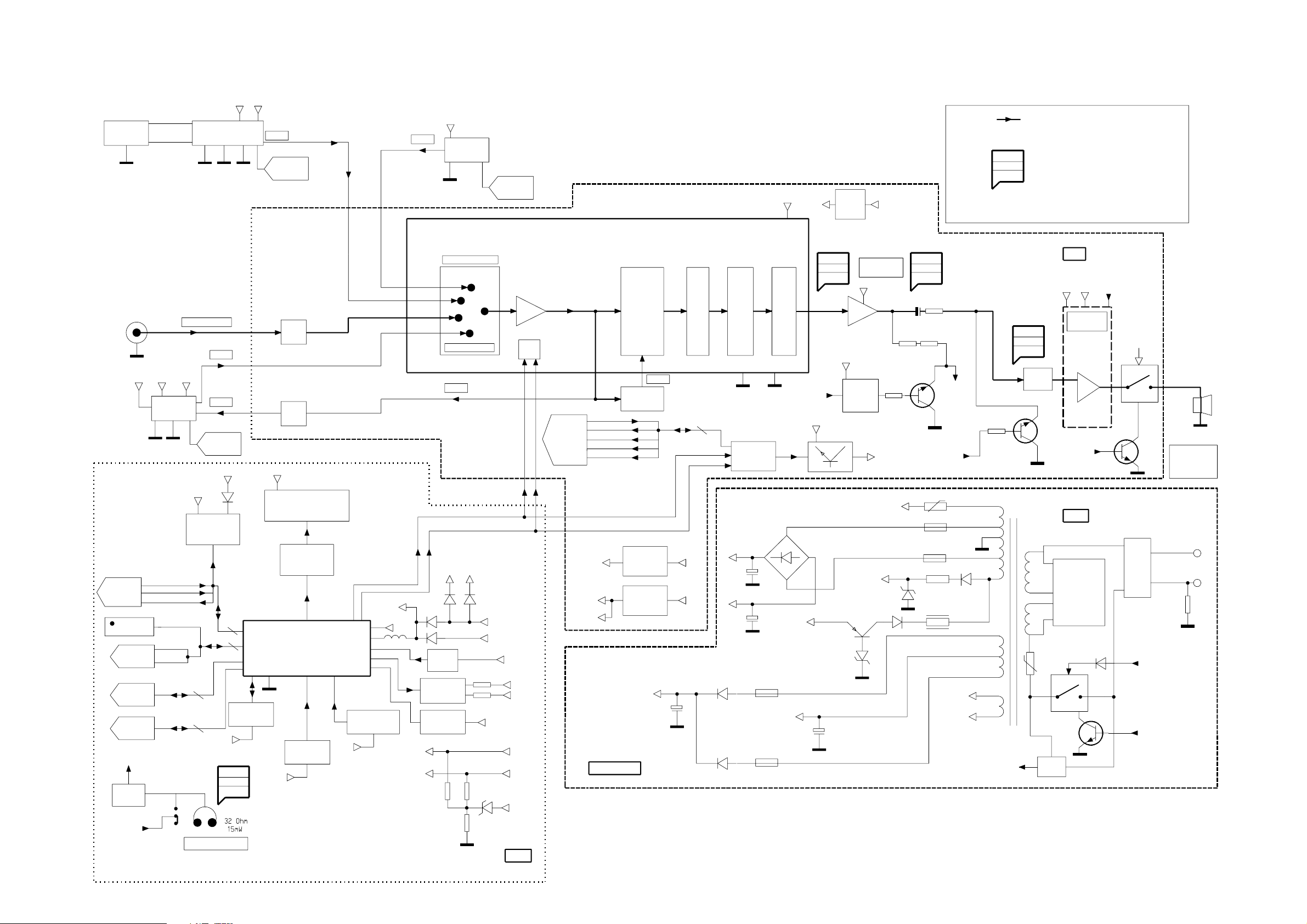
SET BLOCK DIAGRAM
-6dB Track
MP3
D
A
+CD
UL-ICD03
+12V_M
DM
285mV
CDC
CONTROL
4-1
125mV
+12V_A
ECO6
A
FM (67.5 kHz)
AM (80% MOD)
TUNER
CONTROL
TDA7468
+9.1V
+9.1V
+9V
REG
+12V_A
4-1
NOTE :
MAIN SIGNAL PATH
MEASUREMENTS ARE IN AUX MODE :
XX mV
YY dBA
ZZ dB
LEVELS AT MAX VOL
S/N AT 500mW Output
HEADROOM (1% THD) WRT TO LEVEL AT MAX VOL
AUX / CDR
500mV / 1000mV
ATTN.
-8.5dB
A
-CMOS +12V_D
250nWb/m ATTN.
+12V_A
ETF8
125mV
28mV
-25dB
ETF8
CONTROL
+C
ECO POWER
LED
+5V6
+D
SOURCE / VOLUME LEDS
REGISTER
TMP88CU74YF
POWER
CONTROL
RDS
DECODER
TUNER
CONTROL
NTC
PWDN
LPC
AM
SHIFT
uP
SOFTWARE CONTROL
SOURCE SELECTOR
500mV
IIC
500mV
85dBA
16dB
INCREDIBLE
SURROUND
INTERFACE
IIC_CLK1IIC_DATA1
500mV
VOL. 1
SIMPLE
TREBLE
&
BASS
A
VOL. 2
D
LEFT/RIGHT
HP_MUTE
+12V_A
NJM4556AM
+5V6
MUTE
HEADPHONE
AMPLIFIER
2.50V
85dBA
3dB
39R 39R
HP_OUT
1.90V
67dBA
3.0dB
ATTEN.
Rin = 3k
LEFT/RIGHT
COMBI
+AMP
-AMP
POWER
AMPLIFIER
CLASS D
AMP_OFF
+12V_A
IS FILTER
HP_DET
+5V6
+12V_A
+12V_D
MUTE_HP
AMP_OFF
AMP_MUTE
AMP_RELAY
REGULATOR
LM317P
REGULATOR
LM317P
IIC_DATA1
IIC_CLK1
+D2
+D
M62320FP
IIC SHIFT
REGISTER
+AMP
-AMP
COMBI
CONTROL
IIC_CLK1IIC_DATA1
+D
+G
+C
-33V
IR EYE
+5V6
+5V6_ECO
+C
CD_ON
-33V
+5V6
PWDN
+5V_CD
NTC
A
AMP_MUTE
FUSE
FUSE
A
AMP_RELAY
TRAFO
FOR -/21 ONLY
VOLTAGE
SELECTOR
MAINS
CHOKE
(NOT USED FOR -/37)
(ONLY FOR -/37)
LOW_POWER_SUPPLY
L/R SPEAKER
2 X 75W
2 X 6 OHMS
L
N
10M
CONTROL
CONTROL
HP_DET
HP DET
HP_OUT
UL-CD
ETF8
+D
650mV
78dBA
3.2dB
HEADPHONE
EEPROM
D
BASS & TREBLE
CONTROL
ADC
KEY SCAN
+C
+D
+D
FTD
VOLUME
CONTROL
F1x
F2x
F1x
F2x
F1
F2
-33V
FRONT
+D
POWER SUPPLY
FUSE
FUSE
+D2
F1
F2
LOW_POWER_CONTROL
+5V6_ECO
LPS
SMPS
Block Diagram_3139 119 37731_dd wk0409
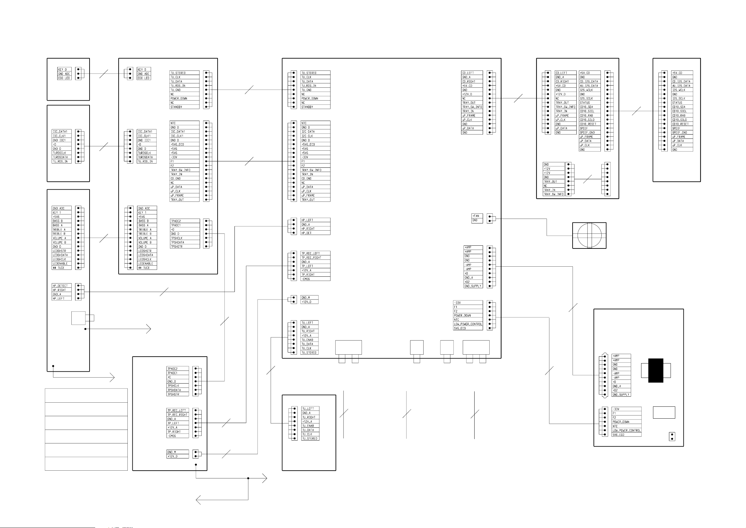
SET WIRING DIAGRAM
5-1
5-1
BI 8008
1
TOP KEY
(CDC KEY)
(1105)
EEPROM
(RDS)
FCT 1600
1
(1105)
FCS 1302
1
8008
3P/180mm
3139 110 36001
8009
8P/100mm/AD
3139 110 34841
8010
15P/120mm/AD
3140 110 20881
EHT 1404
1
FRONT
DISPLAY
(1105)
FCT 1406
1
1
FCS 1405
FCS 1402
FCS 1401
FCT 1407
1
8006
9P/180mm/AD
3139 110 35081
1
1
1
FCT 1012
FCT 1026
FCT 1018
8003
15P/280mm/BD/Fold
3139 111 03871
FCS 1801
FCS 1803
11
8004
19P/98mm/BD
3103 308 93622
FCS 1451
UL-CD
8007
19P/180mm/AD/Fold
3139 111 03881
2 X 75W
(1103)
FCS 1805
1
8001
8P/268mm/AD
3103 308 94021
FCS 1810
MP3
(1106)
COMBI
(1102-1001)
FCT 1014
1
1
1
FCT 1022
EHT 1401
EHT 1010
1
1
2P/260mm
FAN
(1104)
FCS 1300
FRONT
1
1301
HP
8300
8300
1P/220 mm
3139 110 33901
HEADPHONE ESD WIRE
CONTROL
(1105)
## 8301
FRONT CONTROL ESD WIRE
## 8301
1P/220 mm
TO
BOTTOM
PLATE
LEGEND
EHS - EH SIDE ENTRY
EHT - EH TOP ENTRY
FCS - FFC SIDE ENTRY
FCT - FFC TOP ENTRY
BI - BOARD IN ENTRY
8011
4P/280mm/BD
3139 110 34781
TO BOTTOM PLATE’S
PLATE’S LEFT LUG
FCS 1706
FCS 1701
ETF8
EHT 1703
(1107)
FROM TAPE CHASSIS
FROM ALUMINIUM FRONT PANEL
8012
7P/140mm/AD
3139 110 34481
1
1
1
8013
7P/180mm/AD
3139 110 34131
8014
2P/280mm
3139 110 38421
8015
1P/140 mm
3139 111 04291
8015
1P/180 mm
FHT 1020
1
FCT 1013
1
8005
8P/280mm/AD/Fold
3139 110 35241
FCT 1120
1
ECO6
(1101)
TO BOTTOM PLATE’S RIGHT LUG
1005
AUX-IN
8016
1P/160 mm
3139 110 35641
FROM TUNER’S METAL STRIP
TO AUX’S METAL STRIP
ON REARCAB
## 1004
SUBWOOFER OUT
8018
1P/180 mm
3139 110 35791
FROM LEFT CHROME
STRIP TO BOTTOM PLATE’S
LEFT LUG
## 1006
DIGITAL OUT
NOTE : ## - PROVISION
FCT 1011
1
1307
LOUDSPEAKER
8019
2P/180 mm
3139 111 04301
FROM RIGHT & BOTTOM
CHROME STRIPS
TO BOTTOM PLATE’S RIGHT LUG
8001
7P/220mm/AD
3139 110 35901
8303
10P/220mm
3139 110 31571
SUPPLY (MAINS)
(1102-1002)
1
DIP 0201
FCT 1210
1
Wiring Diagram_3139 119 37711_dd wk0409
(5001)
TRAFO
PIN TYPE
LPS
TRAFO
1204
1
N
L

6-1 6-1
FRONT BOARD
TECHNICAL REMARKS
TABLE OF CONTENTS
FTD Display Pin Connection ........................................... 6-2
Display part - Component Layout .................................... 6-3
Display part - Chip Layout ............................................... 6-4
Display part - Circuit Diagram Part 1 .............................. 6-5
Display part - Circuit Diagram Part 2 .............................. 6-6
Display part - Variant Table ............................................. 6-7
Top Key part - Layout & Circuit diagram ......................... 6-7
Control part - Component & Chip Layout ........................ 6-8
Control part - Circuit Diagram Part 1 ............................... 6-9
Control part - Circuit Diagram Part 2 ............................. 6-10
Eeprom part - Layout & Circuit diagram ........................ 6-11
Karaoke part - Component & Chip Layout .................... 6-12
Karaoke part - Circuit Diagram ...................................... 6-13
Electrical parts list.......................................................... 6-14
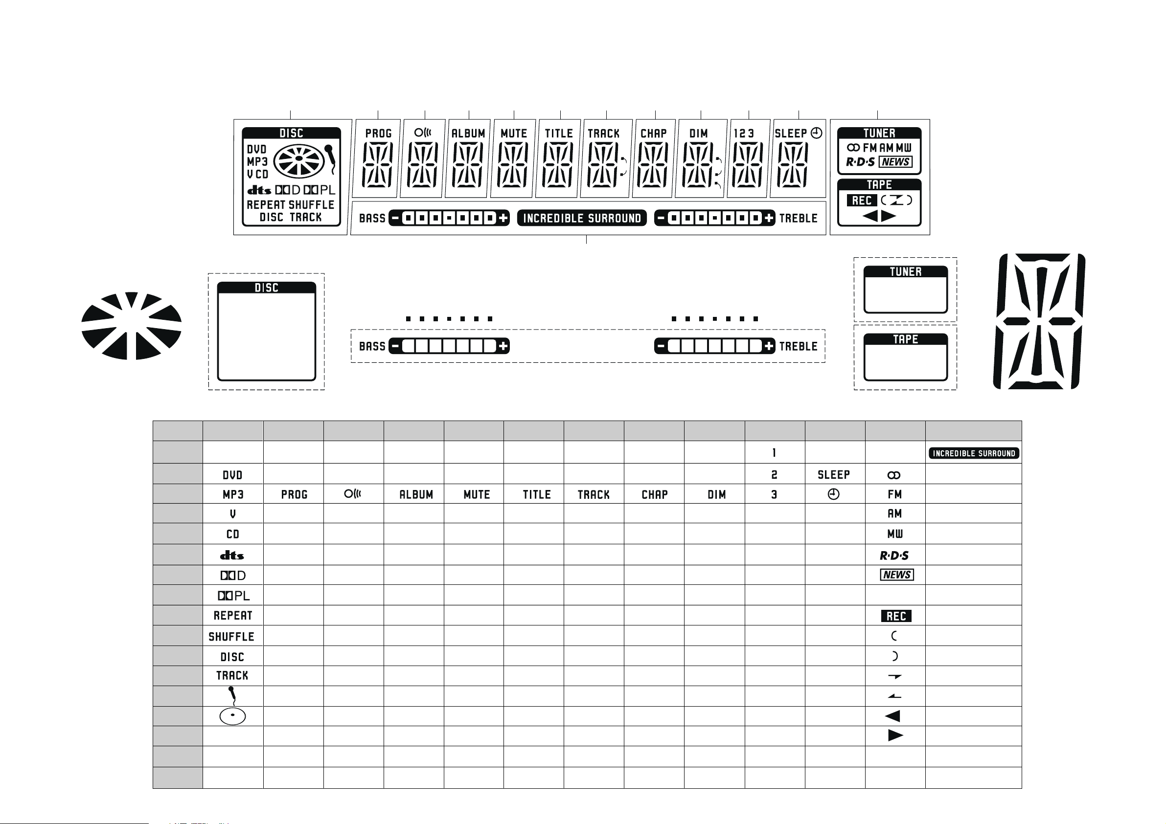
FTD DISPLAY PIN CONNECTION
C1
C2
C3
C4
C5
C6
C7
col
col
dp
6-2
6-2
A
B C
C B
A A
B C
(1G)
1G 2G 3G 4G 5G 6G
B1
B2 B3 B4 B5 B6 B7
S1
(1G)
7G 8G
13G
A1
(13G)
col
9G 10G 11G 12G
col
dp
C1 C2 C3 C4 C5C5C6C6C7
a
hf j k b
S2
g
r
S3
e p n c
d
(12G) (2G - 11G)
m
P1
P2
P3
P4
P5
P6
P7
P8
P9
P10
P11
P12
P13
P14
P15
P16
P17
1G
S1
B
A
C
2G
a
h
j , p
k
b
m
g
c
e
n
d
3G
-
-
-
-
4G
5G
-
-
-
-
6G
7G
-
-
col
-
8G
9G
-
-
col
dp
10G
11G
-
12G
S2
13G
A1
B1
a
h
j , p
k
b
f
r
-
f
m
g
c
e
r
n
d
-
a
h
j , p
k
b
f
m
g
c
e
r
n
d
-
a
h
j , p
k
b
f
m
g
c
e
r
n
d
-
a
h
j , p
k
b
f
m
g
c
e
r
n
d
-
a
h
j , p
k
b
m
g
c
e
n
d
a
h
j , p
k
b
f
r
-
f
m
g
c
e
r
n
d
-
a
h
j , p
k
b
f
m
g
c
e
r
n
d
-
a
h
j , p
k
b
f
m
g
c
e
r
n
d
-
a
h
j , p
k
b
m
g
c
e
n
d
S3
f
r
-
-
-
B2
B3
B4
B5
B6
B7
C1
C2
C3
C4
C5
C6
C7
-
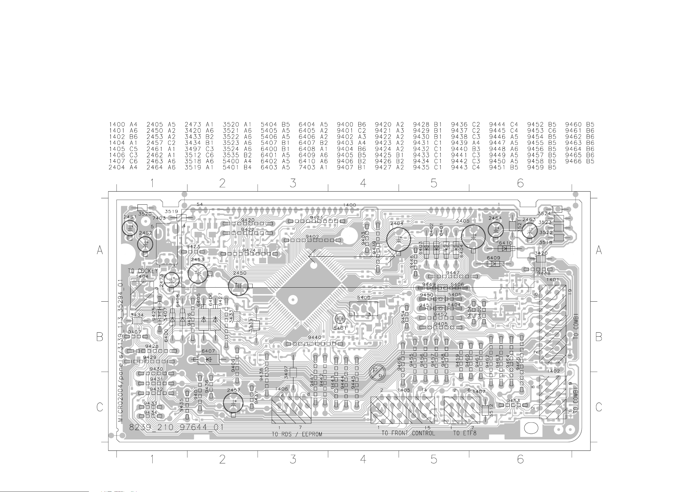
DISPLAY BOARD - COMPONENT LAYOUT
6-3 6-3
This assembly drawing shows a summary of all possible versions. For components used in a specific version see schematic diagram and respective parts list.
3139 113 3529 pt4 dd wk0409
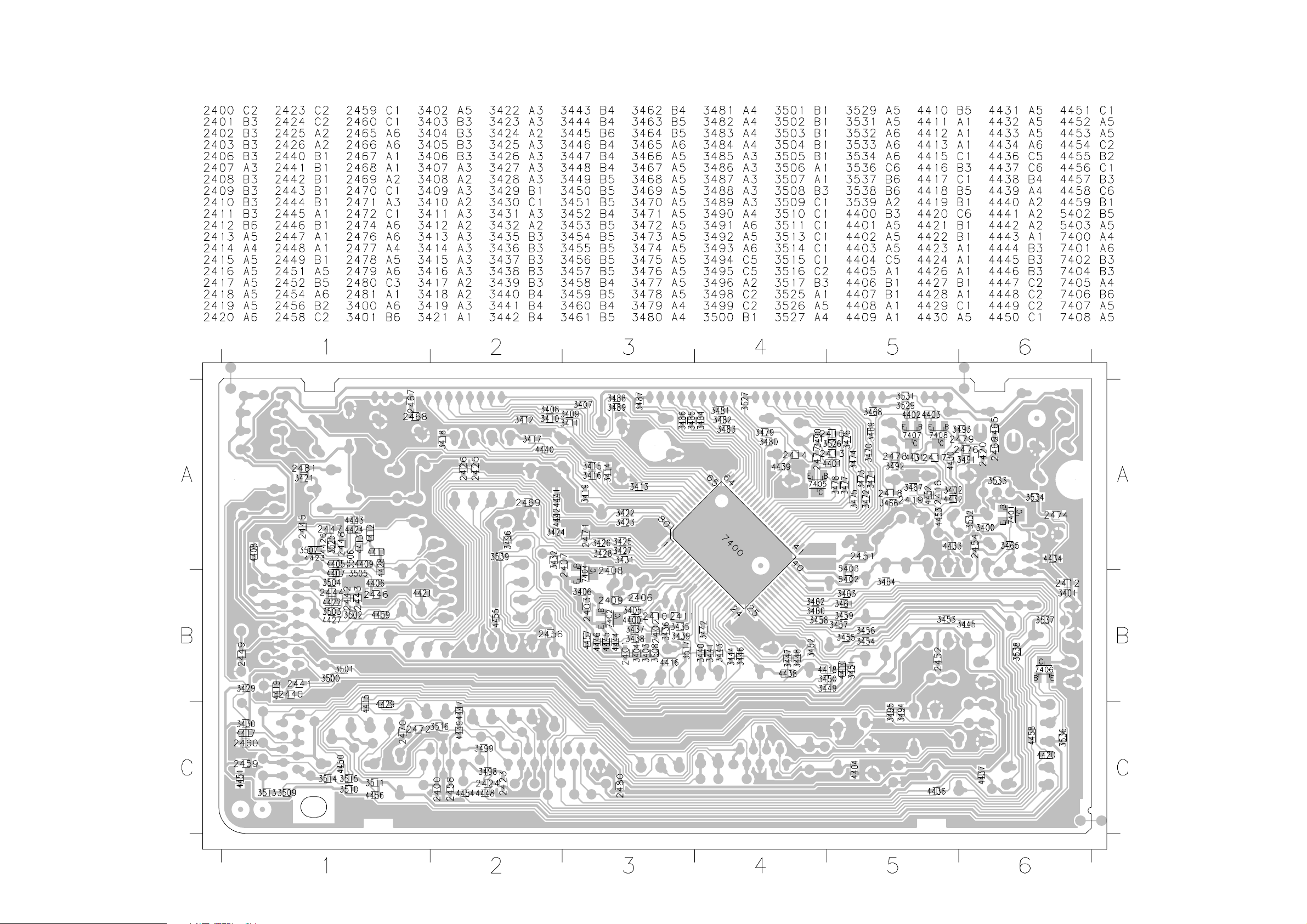
DISPLAY BOARD - CHIP LAYOUT
6-4
6-4
This assembly drawing shows a summary of all possible versions. For components used in a specific version see schematic diagram and respective parts list.
3139 113 3529 pt4 dd wk0409
6-5 6-5
DISPLAY BOARD - CIRCUIT DIAGRAM PART 1
1 234
DVD
7406
BC847B
3536
10K
4415
4429
P12
P13
P14
P15
P16
P17
6401
1N4148
6403
1N4148
##
3429
3430
1K8
1K8
4.6V [4.6V]
7403
TSOP4836ZC1
VS
OUT
GND
4
5
FTD2
3421
3411
1K0
3415
1K0
3417
1K0
6410
1N4148
10K
D
IIC1
3
1
2
A
B
C
D
E
F
G
H
I
ECO LED
BC857B
7401
TO CDC KEY
1404
1
2
3
S3B-EH
TO FRONT CONTROL
1405
1
2
3
4
5
6
7
8
9
10
11
12
13
14
15
15FE-ST-VK-N
RESET
4.9V
3403
100K
D
10n
2403
1 23456
+C
2401
3406
3400
820R
220K
D
6400
1N4148
3401
3404
680K
470n
47K
ECO LED
D
7402
BC847B
+C
+5V6
RC5
+D
TUDATA__DVD_RC6
VolA
TUCLK__DVD_VolA
D
VolB
TUSTEREO__DVD_VolB
D
9425
5407
2u2
100p
+5V6
3465
+C
ADC
D
Key0
2K7
Key1
BassB
BassA
TrebleA
TrebleB
VolA
VolB
LedShStr
LedShClk
LedShData
LedShStr
LedEnable
DVD_INT__TUCE
-33V
#
2412
LedShData
LedShClk
LedEnable
TUCE
TpShStr
TpShData
TpShClk
TUDATA__DVD_RC6
TUCLK__DVD_VolA
TUSTEREO__DVD_VolB
TURdsDATA
+D +D
3405
1K0
10n
2402
Reset
NTC
D
IR EYE
1N4148
6404
1N4148
4404
D
Tray_Out__DVD_TURdsDATA
Only for MCD9/22 Ver
uP_FRAME__DVD_TURdsClk
Only for MCD9/22 Ver
3407
1K0
3408
1K0
3409
1K0
3410
1K0
3412
1K0
3413
10K
3414
10K
6402
3416
1K0
3418
1K0
2404
2405
50V 22u
FTD2
3423
1K0
3425
1K0
3427
1K0
9401
D
10K
2473
3533
D
1K0
3534
2474
2n2
RC5
4416
4418
3419
1K0
50V
4u7
1400 A13
5 6 7 8 9 10 11 12 13
G12x
#
49
G13x
3491
#
4403
F2b
53
54
10K
1400
HNA-13SM42
F2a
+G
100p
2419
7408
BC847B
82K
3493
2479
100p
#
TO RDS / EEPROM
1406
08FE-ST-VK-N
TO ETF8
1407
1
TPADC2
2
TPADC1
3
+C
4
GND_D
5
TPSHCLK
6
TPSHDATA
7
TPSHSTROBE
FE-ST-VK-N
-26.5V
(-26.9V)
1
2
3
4
5
6
7
8
G13x
3531
2420
FTD1
-33V
A
B
100R
C
100p
D
E
F
G
H
I
Note : Some values may varies, see respective parts list for correct value.
DC Voltages During Active Play.Note :
Values in Square Bracket are DC Voltages at ECO-Standby.
Values in Bracket are DC Voltages at Standby (Clock Mode).
TURdsDATA
Legend :
TURdsClk
P6
P7
P8
P9
P10
P11
1K0
3489
3487
1K0
3488
65
66
67
68
69
70
71
72
73
74
75
76
77
78
79
80
50V 22u
3422
1K0
3424
1K0
3426
1K0
4457
V24
V25
V26
V27
V28
V29
V30
V31
V32
V33
V34
V35
V36
VKK
-SCK1
SI1
1
V23
SO1
V21
V22
80k pull
8-Bit h. breakdown v.
out. port w. latch P9
PD
source open
5-Bit h. breakd. v.
out w. latch
8-Bit Input/Output
(tri-state)
P03
P04
3
3428
1K0
ADC
3496
4.9V
3532
+C
100R
D
D
1K0
1K0
3485
1K0
3486
3484
V18
V19
V20
8-Bit h. break. v.
down
drain 80k p.d.
P0
P05
P06
P07
4
1K0
3431
4K7
10K
3432
33p
2407
P5
P4
1K0
3483
1K0
V17
VFT driver circuit (automatic display)
VSS
8
7
D
5400
2406
D
7404
BC847B
D
Refer to Variant Table.
#
For Provision Only .
P1
P2
P3
1K0
3481
1K0
3482
V16
V15
8-Bit high breakdown voltage 8-Bit high breakdown v.
output port with latch output port with latchout w. latch P8
3480
V14
3479
1K0
V13
G2
G1
1K0
3477
1K0
3478
V11
V12
G3
1K0
3476
51525354555657585966061626364
V10
P7 P6
80k pull down80k pull down
P6-P9 source open drain
ROMRAM
CPU
drain
sink o.
8-Bit I/O P2
sink o.drain
XIN
XOUT
-RESET
TEST
XTIN
XTOUT
9
10 11 12 13 14 15 16 17 18 19220 21 22
32K768
2410
D
22p
22p
2408
Option
Reset
5401
-STOP
22p
D
D
22p
2411
D
2p2
2409
D
3433
2K7
3434
180R
G6
G5
G4
1K0
3473
3475
1K0
1K0
3474
V7
V8
V9
Program
Counter
8-Bit Input/Output
(tri state)
TC2
-INT0
-INT1
+C
D
G7
G8
1K0
3471
1K0
3472
V6
8-Bit A/D
Converter
TC4
-DV0
POWER-DOWN
FTD1
G9
1K0
3470
V4
V5
P1
TC1
3435
1K0
80k pull down
9402 9403
D
G10
G13
G12
G11
1K0
1K0
3469
3467
1K0
1K0
3468
414243444546474849550
V1
V2
V3
VAREF
VASS
AIN13
P5
AIN12
AIN10
4-Bit In/Output
(tri-state)
P4
8-Bit Input/Output
(tri-state)
3-B. I/O P3
( tristate )
-SCKO
INT4
INT2
SCL
23 24
1M0
3436
1K0
3466
V0
VDD
AIN11
AIN7
AIN6
AIN5
AIN4
AIN3
AIN2
AIN1
AIN0
SCA
TMP88CU74F
7400
3448
470R
3445
1K0
3444
1K0
3442
100R
3440
1K0
D
FTD2
4.9V [4.9V]
40
39
4.9V [4.9V]
38
37
36
35
34
33
32
31
30
29
28
27
26
25
3437
680K
4400
3447
470R
3446
470R
3443
100R
3441
1K0
3439
1K0
3464
470R
3462
3460
3458
3456
3454
3452
470R
P1
P2
1G372G
34P333P432P531P630P729P828P927
35
383G394G405G416G427G43
P1
P2
P3
P6
P4
P5
G1x
+G
G12x
44
G8G7G6G5G4G3G2
G13
8G
45
G9
9G
10G4611G4712G4813G
G10
G11
-33V
#
3529
3492
+D
6K8
IIC1
7407
BC847B
82K
3495
2418
6K8
+D
100R
100p
FTD1
2476
100p
10K
2417
100p
100p
2478
#
3494
D
P14
P13
P15
+G
7405
BC847B
82K
3490
IIC_DATA1
IIC_CLK1
TpADC2
TpADC1
P11
P12
VolA
VolB
NTC
BassB
BassA
Option
Key0
Key1
G1x
3527
2414
+D
P1013P1112P1211P1310P149P158P167P17
P10
D
G12
100R
100p
FTD1
IIC_DATA1
IIC_CLK1
TURdsClk
TURdsDATA
TU_RDS_In
P7
P9
P8
#
#
2416
100p
3402
4402
#
F1a
F1b
6
1
2
-26.5V
F1x F2x
(-26.9V)
-33V -33V
#
#
100p
2415
3526
P16
P17
10K
2413
100p
G1
4401
#
100p
2477
#
+C
ADC
+H
2K7
3535
100p
2480
+C
D
3463
470R
1K0
3461
1K0
1K0
3459
1K0
1K0
3457
1K0
1K0
3455
1K0
1K0
3453
1K0
4410
10K
10K
3450
3449
DVD
3537
10K
3538
9407
10K
4458
4420
uP_FRAME__DVD_TURdsClk
3451
10K
9406
uP_CLK__IIC_CLK3
uP_DATA__IIC_DATA3
RC5
Tray_SW_Info
4438
TURdsClk
Tray_In__DVD_Power_On
Tray_Out__DVD_TURdsDATA
Standby
TrebleB
TrebleA
TpADC2
TpADC1
+C
TpShClk
TpShData
3499
100R
3498
100R
TpShStr
10K
3539
3438
1M0
D
D
3497
10K
DVD
D
PWDN
D
47p
100n
2423
2424
2458
# FOR PROVISION ONLY
47p
47p
47p
2425
2426
2400
47p
D
8239_210_97644_01 (Display Circuit 1)...for 3529 pt4 dd wk0409
1404 C1
1405 E1
1406 E13
1407 G13
2400 H12
2401 H1
2402 H2
2403 I1
2404 F4
2405 F4
2406 G6
2407 H5
2408 H6
2409 H6
2410 G6
2411 G6
2412 C2
2413 C10
2414 C10
2415 C9
2416 C11
2417 C11
2418 C12
2419 C13
2420 C13
2423 H11
2424 H12
2425 H12
2426 H12
2458 H11
2473 H4
2474 I4
2476 C12
2477 C10
2478 C11
2479 C13
2480 D9
3400 A1
3401 B1
3402 C11
3403 H1
3404 H1
3405 H2
3406 I1
3407 C4
3408 C4
3409 C4
3410 D4
3411 D3
3412 D4
3413 D4
3414 E4
3415 E3
3416 E4
3417 E3
3418 F4
3419 F4
3421 F3
3422 G4
3423 G4
3424 G4
3425 G4
3426 G4
3427 G4
3428 G5
3429 H3
3430 H3
3431 H5
3432 H5
3433 H7
3434 I7
3435 H8
3436 I8
3437 H9
3438 I9
3439 H9
3440 H8
3441 H9
3442 G8
3443 G9
3444 G8
3445 G8
3446 G9
3447 G9
3448 G8
3449 F9
3450 F9
3451 F10
3452 F9
3453 F9
3454 F9
3455 F9
3456 F9
3457 E9
3458 E9
3459 E9
3460 E9
3461 E9
3462 E9
3463 E9
3464 D9
3465 C2
3466 C8
3467 C8
3468 C8
3469 C8
3470 C8
3471 C7
3472 C7
3473 C7
3474 C7
3475 C7
3476 C7
3477 C7
3478 C6
3479 C6
3480 C6
3481 C6
3482 C6
3483 C6
3484 C6
3485 C5
3486 C5
3487 C5
3488 C5
3489 C5
3490 C10
3491 C13
3492 C12
3493 C13
3494 E12
3495 E12
3496 H5
3497 H10
3498 G12
3499 G12
3526 C10
3527 C10
3529 C12
3531 C13
3532 H4
3533 H4
3534 I4
3535 D9
3536 A3
3537 D10
3538 D10
3539 H9
4400 I9
4401 C10
4402 C11
4403 C13
4404 H4
4410 F9
4415 B3
4416 B4
4418 B4
4420 E10
4429 B3
4438 G10
4457 G5
4458 E10
5400 G6
5401 G6
5407 C2
6400 A1
6401 E3
6402 E4
6403 E3
6404 F4
6410 F3
7400 G8
7401 B1
7402 H1
7403 H3
7404 H6
7405 C10
7406 A3
7407 C12
7408 C13
9401 H4
9402 B8
9403 B8
9406 G10
9407 D10
9425 C2
789101112 13
6-6
DISPLAY BOARD - CIRCUIT DIAGRAM PART 2
6-6
1401 A3
1402 B11
2440 B5
2441 B6
2442 C6
2443 C5
2444 C5
2445 D4
2446 D4
2447 D5
2448 D5
2449 F2
2450 F3
2451 F3
2452 F2
2453 F2
123456789101112
A
DVD
B
C
D
IIC_CLK3
IIC_DATA3
GND_IIC3
DVD_POWER_ON
NC
DVD_I NT
DVD_TURDS_CLK
DVD_TURDS_DATA
NOTE : DVD_TURDS_CLK & DVD_TURDS_DATA ARE FOR MCD9/22 VERSION
MP3
NTC
GND_IIC1
IIC_DATA1
IIC_CLK1
GND_D
+5V6_ECO
+5V6
+5V6
-33V
F1
F2
SW_INFO
TRAY_IN
CD_GND
NC
uP_DATA
uP_CLK
uP_FRAME
TRAY_OUT
E
+5V6_ECO
#
2449
F
+5V6
#
2452
G
2454 F3
2456 F3
2457 F5
2459 F5
6405
1N4003
100n
D
6406
1N4003
100n
D
2460 C9
2461 E10
2462 E10
2463 F10
TO COMBI
1401
1
2
3
4
5
6
7
8
9
10
11
12
13
14
15
16
17
18
19
FE-ST-VK-N
16V47u
2453
#
5402
4u7
5403
4u7
2454
100n
2464 F10
2465 E10
2466 E10
2467 F10
16V47u
2450
D
D
#
2451
2456
2468 F10
2469 C8
2470 C8
2471 C9
+H
100n
+C
100n
2472 C9
2481 C7
3420 C8
3500 B5
I2C1
D
+5V6_ECO
+5V6
5.6V
-33V
-33V
F1
F2
4408
#
4459
3504
#
470R
3506
#
470R
4405
D
+5V
+5V
3501 B5
3502 B6
3503 C5
3504 C4
#
4419
I2C1
0V [5.6V]
4427
3503
220R
4422
4407
#
3505
470R
#
3507
470R
4423
10p
10p
2446
2445
# FOR ESD PROVISION ONLY
+5V6
+5V6
6407
1N4003
6408
1N4148
3505 D4
3506 D4
3507 D4
3508 B8
IIC1
# ESD PROVISION
D
4428
4411
4412
#
10p
2448
2447
2457
3509 B8
3510 B8
3511 B9
3512 B9
3513 B10
3514 B9
3515 B10
3516 B9
3517 C8
3518 E9
3519 D9
3520 E9
3521 F9
3522 F8
3523 F9
3524 F9
3525 D6
4405 D4
4406 D5
4407 C4
NTC
10p
2440
2441
#
#
3500
220R
3501
220R
2442
2443
10p
10p
D
2444
100n
4406
#
4409
5406
2u2
9449
3502 -> 220R for MCD9
10p
IIC1
3502
470R
9405
Tray_SW_Info
IIC_DATA1
IIC_CLK1
Tray_In__DVD_Power_On
9400
9404
5404
uP_DATA__IIC_DATA3
2u2
9451
5405
2u2
9450
4421
uP_CLK__IIC_CLK3
uP_FRAME__DVD_TURdsClk
TUSTEREO__DVD_VolB
TUCLK__DVD_VolA
TUDATA__DVD_RC6
TUCE
TU_RDS_In
DVD_INT__TUCE
PWDN
Standby
Tray_Out__DVD_TURdsDATA
#
3525
2459
470R
4426
+D
100n
10p
16V47u
#
4424
DVD_INT__TUCE
4413
+5V
D
+G
Note : Some values may varies, see respective parts list for correct value.
DC Voltages During Active Play.Note :
Values in Square Bracket are DC Voltages at ECO-Standby.
Legend :
Refer to Variant Table.
#
For Provision Only .
4408 C4
4409 D5
4411 D5
4412 D5
47p
2481
(MCM5) 4.7Vac
(MCM7) 4.7Vac
(MCM8) 4.0Vac
(MCD9) 4.7Vac
4413 E6
4417 C10
4419 A4
4421 C6
3420
1K0
D
10K
47p
3510
2470
4427 C5
4428 D5
4459 C4
5402 E3
+D
10K
47p
3517
+C
3508
47K
4422 C5
4423 D4
4424 D6
4426 E6
39K
3509
2469
# FOR ESD PROVISION ONLY
F2
F1
3522
220R
6409
BZX79-B6V8
-33V
3511
2471
3518
3521
10K
#
3516
1K0
47p
220R
22K
FTD2
5403 F3
5404 C6
5405 D6
5406 D6
#
10K
3512
#
47p
2472
3514
1K0
9453
3519
2R2
3520
2R2
3523
2R2
3524
2R2
6405 E2
6406 F2
6407 E4
6408 F4
2460
100p
3513
1K0
3515
1K0
4417
2461
2462
2463
2464
6409 G8
9400 C6
9404 C6
9405 B6
4u7
2465
50V
#
2466
50V 4u7
#
FTD1
4u7
2467
50V
#
4u7
2468
50V
#
FTD2
220p
220p
220p
220p
9449 D6
9450 D6
9451 D6
9453 B9
F2x
F1x
TO COMBI
1402
1
2
3
4
5
6
7
8
9
FE-ST-VK-N
(MCM5) 4.4Vac
(MCM7) 4.4Vac
(MCM8) 3.9Vac
(MCD9) 4.4Vac
DVD
DVD_VOLB
DVD_VOL A
DVD_RC6
TU_RDS_IN
TU_GND
NC
POWER_DOWN
NC
STANDBY
8239_210_97644_01 (Display Circuit 2)...for 3529 pt4 dd wk0409
MP3
TU_STEREO
TU_CLK
TU_DATA
TU_RDS_IN
TU_GND
NC
POWER_DOWN
NC
STANDBY
A
B
C
D
E
F
G
123
456789
10 11 12
This assembly drawing shows a summary of all possible versions. For components used in a specific version see schematic diagram and respective parts list.
3139 113 3529 pt4 dd wk0409
6-7 6-7
DISPLAY BOARD - VARIANT TABLE
MCM7/22 MCM8/22
MCM7/25
2444
100N 100N
3434
1M
3437
680K
3438
3496
-
-
3503
39K3508 39K
3519
3520 2R22R2 1R1R
3523
MCM7/37
180R
1M 2M23436
680K
1M1M
10K
10K 10K3497
--
2R22R2
2R22R2
MCM8/25
100N
470R 470R180R
MCM8/21
100N
2M2
--
-
-
-
10K
-
--
-1R1R
1R1R
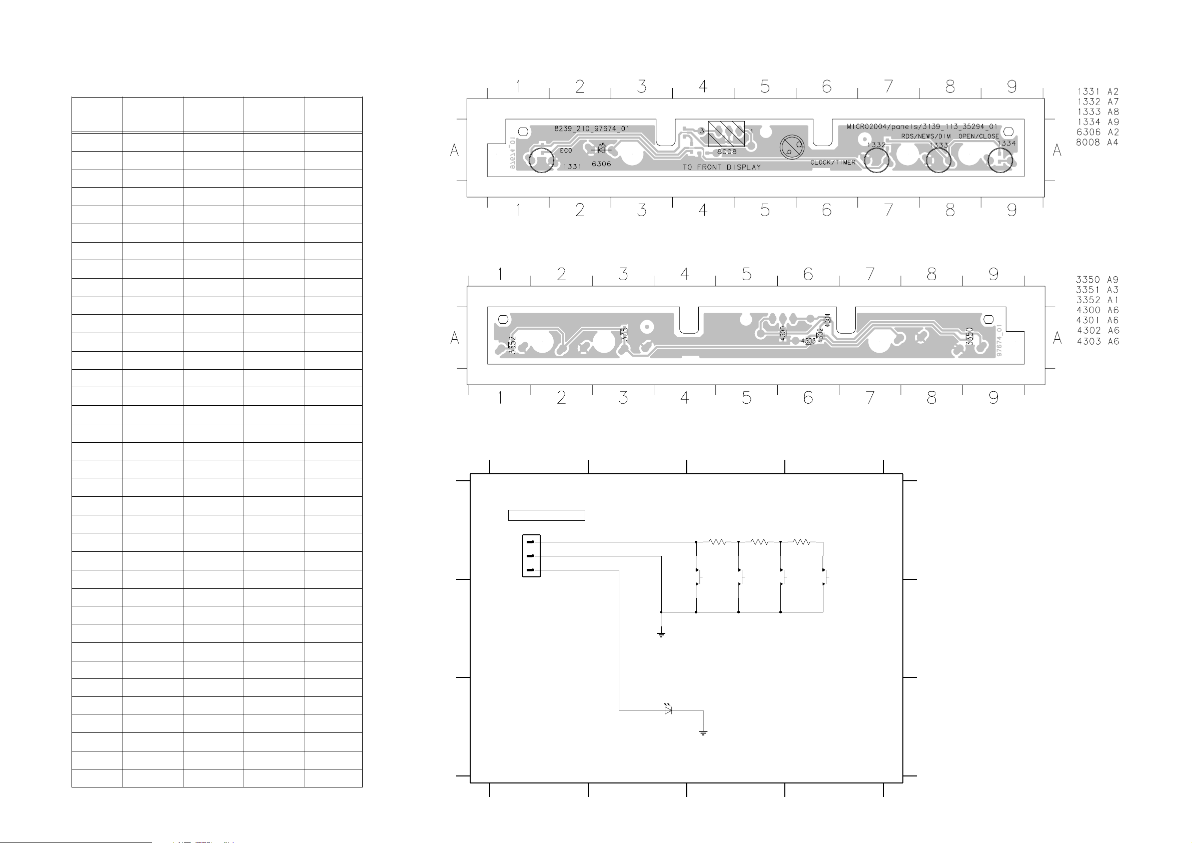
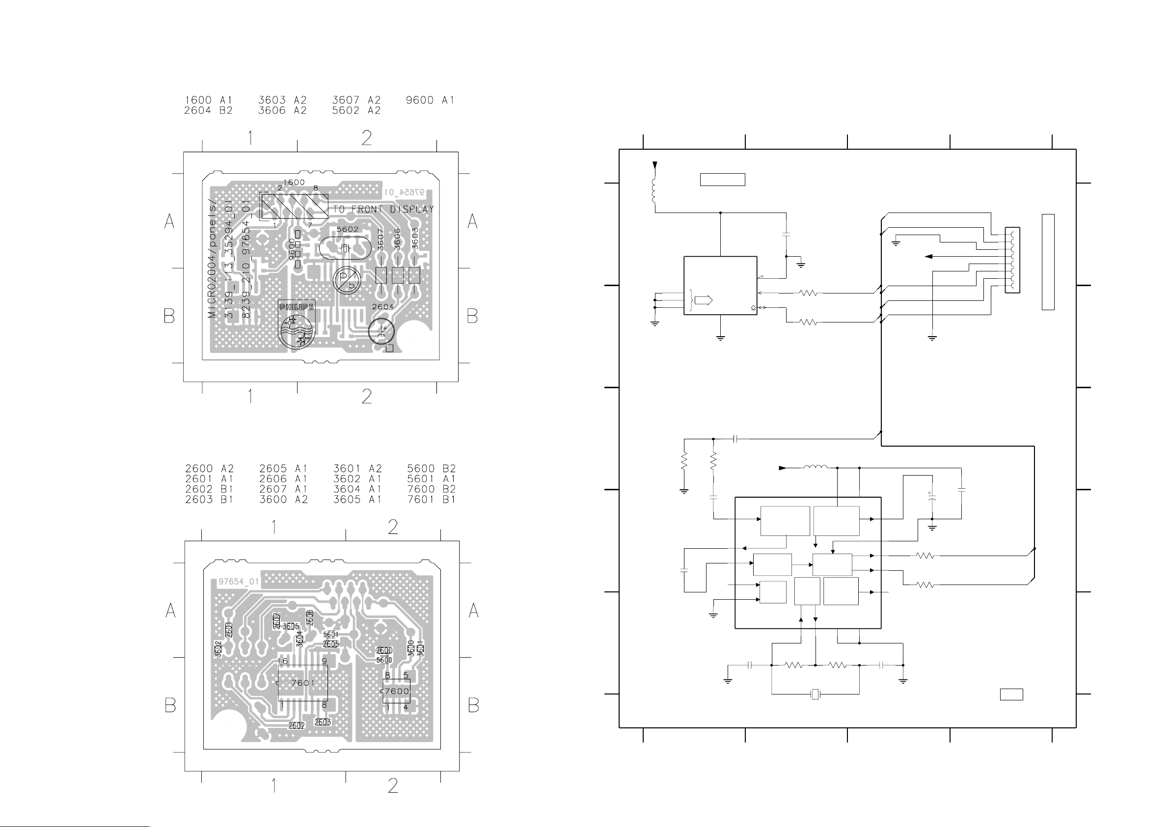
TOP KEY BOARD - COMPONENT LAYOUT
This assembly drawing shows a summary of all possible versions. For components used in a specific version see schematic diagram and respective parts list.
3139 113 3529 pt4 dd wk0409
TOP KEY BOARD - CHIP LAYOUT
3524 2R22R2 1R1R
4400
4406
4409
4411
4413
4420
4421
4422
4424
4427
4438
4457
4458
4459
--
XXXX
XXXX
XXXX
----
XXXX
XXXX
----
XXXX
XXXX
XX
XX
--
--
XXX
----
XX
5404 2U2 2U2 2U22U2
5405
2U2
2U2
2U2
X
2U2
TOP KEY BOARD - CIRCUIT DIAGRAM
1234
TO FRONT DISPLAY
A
8008
35022
1
2
3
Key0
B
ADC
ECO
SKQNAB
CLOCK / TIMER
3350
150R
1331
SKQNAB
RDS / NEWS / DIM
OPEN / CLOSE
SKQNAB
3352
270R
1333
3351
220R
1332
SKQNAB
1334
A
B
1331 A3
1332 A3
1333 A4
1334 A4
3350 A3
3351 A3
3352 A4
6306 C2
8008 A1
5406
9400
9404
9405 XXXX
9449
9450
9451
X - Item in use.
2U2
2U2
2U2
2U2
----
--
--
----
----
----
C
Note : Some values may varies, see respective parts list for correct value.
1234
ECO LED
6306
LTL-816EELC
ADC
C
8239_210_97674_01...for 3529 pt4 dd wk0409
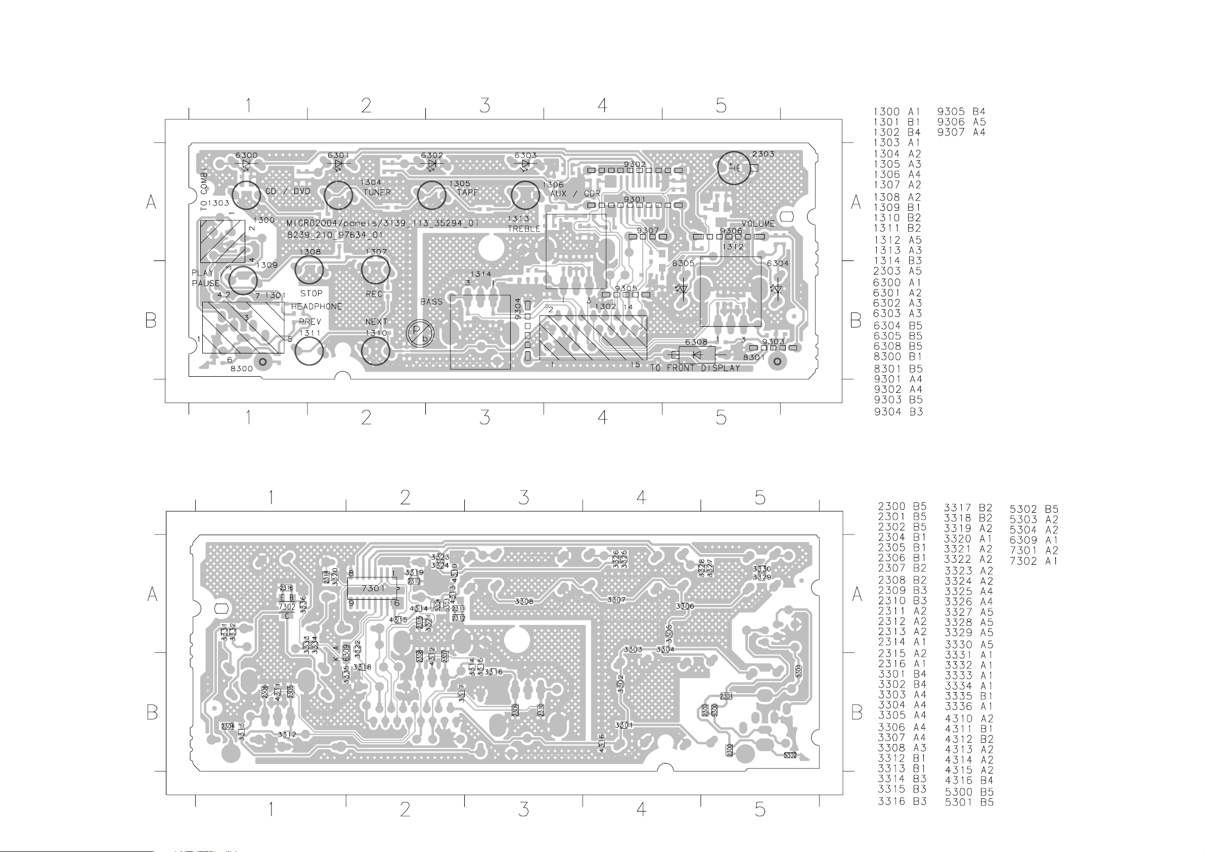
CONTROL BOARD - COMPONENT LAYOUT
This assembly drawing shows a summary of all possible versions. For components used in a specific version see schematic diagram and respective parts list.
6-8
6-8
CONTROL BOARD - CHIP LAYOUT
This assembly drawing shows a summary of all possible versions. For components used in a specific version see schematic diagram and respective parts list.
3139 113 3529 pt4 dd wk0409
3139 113 3529 pt4 dd wk0409

6-9 6-9
CONTROL BOARD - CIRCUIT DIAGRAM PART 1
A
B
1300 A7
1301 A9
1302 A1
1303 A5
1304 A5
1305 A5
TO FRONT DISPLAY
1302
1
2
3
4
5
6
7
8
9
10
11
12
13
14
15
15FE-ST-VK-N
1306 A6
1307 A3
1308 A4
1309 A4
1310 A3
1311 A3
1312 E2
1313 E4
1314 E5
2300 B8
2301 A8
2302 A9
2304 E2
2305 E3
2306 E3
2307 E4
2308 E5
2309 E6
2310 E6
3301 A3
3302 A3
3303 A4
3304 A4
3305 A4
3306 A5
3307 A5
3308 A5
3312 D3
3313 D3
3314 D4
3315 D5
3316 D6
3317 D6
5300 A8
5301 A8
5302 B8
6308 D2
8300 B7
8301 E2
123456789
FRONT CONTROL PANEL KEYS
Key1
+5V6
BassB
BassA
TrebleA
TrebleB
VolA
VolB
D
LedShStr
LedShData
LedShClk
LedEnable
TUCE
ADC
Key1
NEXT
150R
SKQNAB
3301
1310
ADC
PREV
SKQNAB
3302
220R
1311
REC
3303
270R
SKQNAB
1307
STOP
SKQNAB
3304
390R
1308
3305
560R
SKQNAB
1309
CD
3306
820R
SKQNAB
1303
TUNERPLAY / PAUSE
3307
1K2
SKQNAB
1304
TAPE
SKQNAB
AUX / CDR
3308
1K8
1305
SKQNAB
1306
TO COMBI
1300
1
2
3
4
FE-ST-VK-N
8300
1
RT-01T-1.0B
HEADPHONE ESD WIRE
TO BOTTOM PLATE
HP
HP_DETECT
HP_RIGHT
HP_GND
HP_LEFT
5300
2u2
5301
2u2
5302
2u2
2300
100n
2301
22n
2302
HP
22n
HEADPHONE
1301
4
2
7
1
6
3
5
TC38-103-61
A
B
C
D
E
VolA
VolB
VOLUME
8301
6308
1N4003
2304
#
100n
+D
1312
EC12
1B3
A
C
5
2
4
D
+5V6
#
1
RT-01T-1.0B
PROVISION FOR ESD WIRE TO BOTTOM PLATE
3312
2305
+D
10K
10n
4.9V
3313
2306
D
10K
10n
TREBLE
1313
EVE
4
TrebleA
1A3
C
5
D
TrebleB
B
2
3314
2307
+D
10K
10n
4.9V
3315
2308
D
10K
10n
BASS
1314
EVE
C
LedEnable
BassB
BassA
LedShStr
+D
4.9V
LedShData
LedShClk
10K
10n
3317
2310
D
10K
10n
TUCE
# : PROVISION
Note : Some values may varies, see respective parts list for correct value.
3316
1A3
B
C
2
4
5
2309
D
LedEnable
LedShStr
LedShData
LedShClk
TUCE
D
E
8239_210_97634_01 (Control Circuit 1)...for 3529 pt4 dd wk0409
123456789
6-10
CONTROL BOARD - CIRCUIT DIAGRAM PART 2
6-10
A
B
C
D
2303 D5
2311 A4
2312 A4
2313 C3
2314 C3
2315 D3
2316 C8
3318 B2
3319 C2
3320 C2
3321 D2
3322 E2
3323 B5
3324 B6
3325 B6
3326 B6
3327 B7
3328 B7
3329 B7
3330 B8
3331 B8
3332 B8
3333 B9
3334 B9
3335 D5
3336 C5
5303 A3
5304 A3
6300 B8
6301 B7
6302 B6
6303 B5
6304 B8
6305 B9
6309 C5
7301 B3
7302 C9
1234567
5303
4u7
5304
4u7
7301
74HC4094D
15
EN1
1
STB
3
2
D1
SRG8
16
2311
100n
2312
100n
1K5
3323
D
3324
1K5
3325
AUX / CDR
1K5
3326
1K5
TUNERTAPE
3327
1K5
3328
CD / DVD
1K5
3329
1K5
3330
AUX / CDR
4
5
6
7
TAPE
TUNER
CD
6303
LTL-816TDK3
D
6302
LTL-816TDK3
D
14
13
12
11
9
10
8
D
6309
BAS316
3335
10K
D
2303
10V100u
3336
10K
VOLUME
6301
LTL-816TDK3
6300
LTL-816TDK3
LedEnable
LedShStr
LedShClk
LedShData
3318
3319
3320
3321
D
D
D
10K
10K
10K
10K
2313
2314
2315
+5V6
47p
D
47p
D
47p
89
+5V6+5V6 +5V6
1K5
3331
390R
6304
2316
#
3332
390R
LTL-816TDK3
22p
D
7302
BC847B
D
3333
390R
6305
VOLUME
3334
390R
LTL-816TDK3
A
B
C
D
E
# : PROVISION
Note : Some values may varies, see respective parts list for correct value.
TUCE
3322
#
1K0
D
D
E
8239_210_97634_01 (Control Circuit 2)...for 3529 pt4 dd wk0409
123456789
6-11
6-11
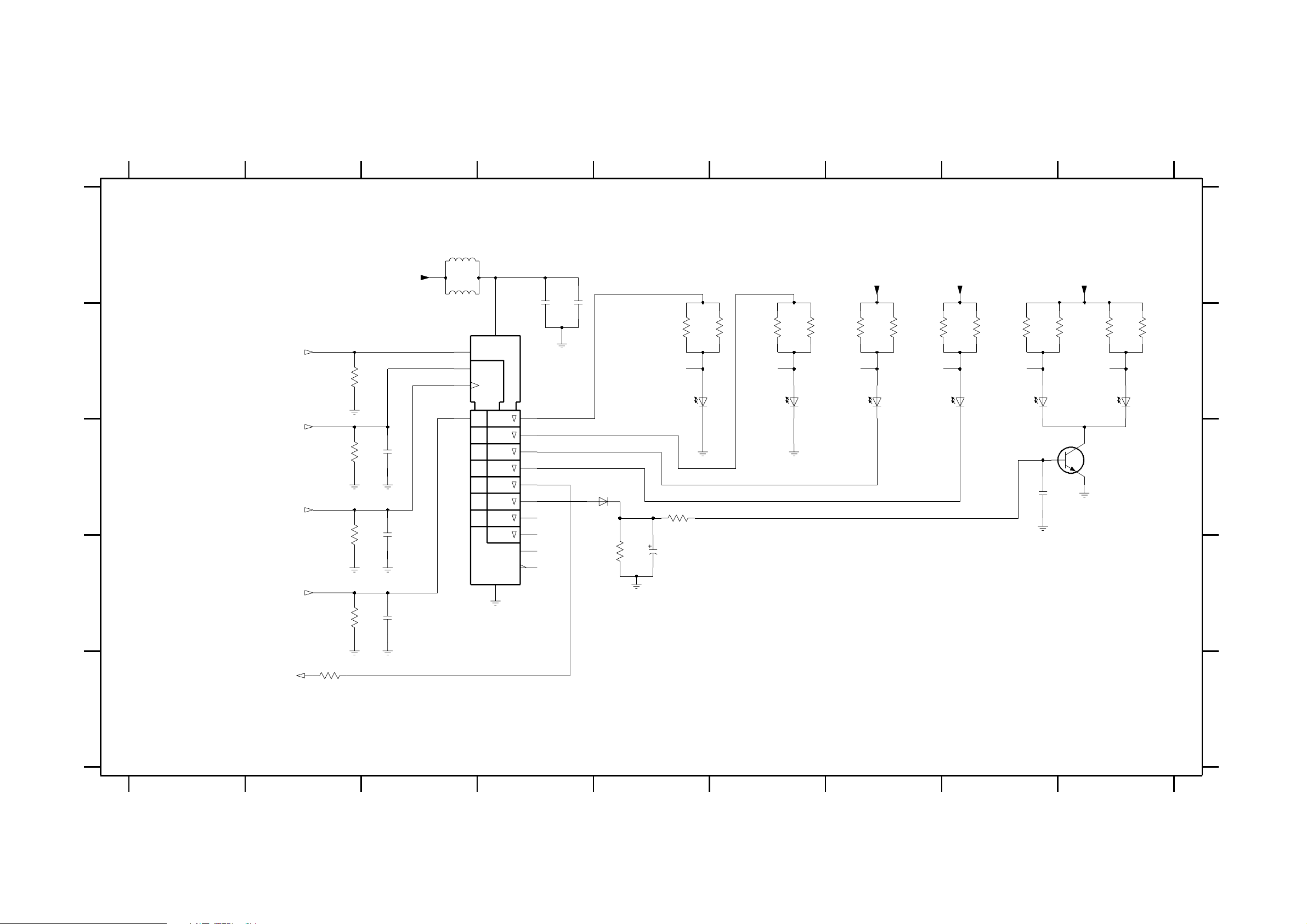
EEPROM BOARD - CIRCUIT DIAGRAMEEPROM BOARD - COMPONENT LAYOUT
This assembly drawing shows a summary of all possible versions.
For components used in a specific version see schematic diagram and respective parts list.
3139 113 3529 pt4 dd wk0409
A
B
1600 A4
2600 A2
2601 C1
2602 D1
+D
2u2
5600
7600
M24C02-WMN6
1
2
3
IIC1
2603 D1
2604 D3
2605 D4
2606 E2
2607 E3
3600 B2
3601 B2
3602 C1
3603 C1
3604 E2
3605 E2
3606 D3
3607 D3
5600 A1
5601 C2
5602 E2
7600 A1
7601 C1
1234
EEPROM
IIC_DATA1
4.9V
84
Φ
(256x8)
EEPROM
0
ADR
1
2 SDA
IIC1
WC
SCL
IIC_CLK1
100n
2600
3600
1K0
3601
1K0
IIC1
IIC_CLK1
IIC_DATA1
7
6
5
IIC1
4.9V
+D
TURdsClk
TURdsData
TU_RDS_In
D
1600
1
2
3
4
5
6
7
8
08FE-BT-VK-N
TO FRONT DISPLAY
A
B
EEPROM BOARD - CHIP LAYOUT
This assembly drawing shows a summary of all possible versions.
For components used in a specific version see schematic diagram and respective parts list.
2601
C
D
3602
2603
10K
D
560p
3603
2602
1n0
1K5
7601
SAA6581T
560p
4
8
7
15
9
MPX
SCOUT
CIN
TCON
MODE
+D
57 Khz
BANDPASS
(8th ORDER)
CLOCKED
COMP
TEST
CTRL
D
E
2606
47p
DD
Note : Some values may varies, see respective parts list for correct value.
3604
220K
5601
VSSA
OSC
&
CLK
OSCI
13
5602
AT-51
TU_RDS_In
2u2
512
VDDA
POW SUPPL
&
RESET
RDS/RBDS
DEM
SIGNAL
QUALITY
DET
VSSA
OSCO
611
14
3605
2K2
4M332
4.9V
VDDD
VREF
SYNC
RDCL
RDDA
QUAL
VSSD
2607
47p
3
10
16
2
1
50V
100n
2605
2604
2u2
D
3607
1K0
3606
1K0
TURdsClk
TURdsData
RDS
8239_210_97654_01...for 3529 pt4 dd wk0409
C
D
E
3139 113 3529 pt4 dd wk0409
1234
6-12
6-12
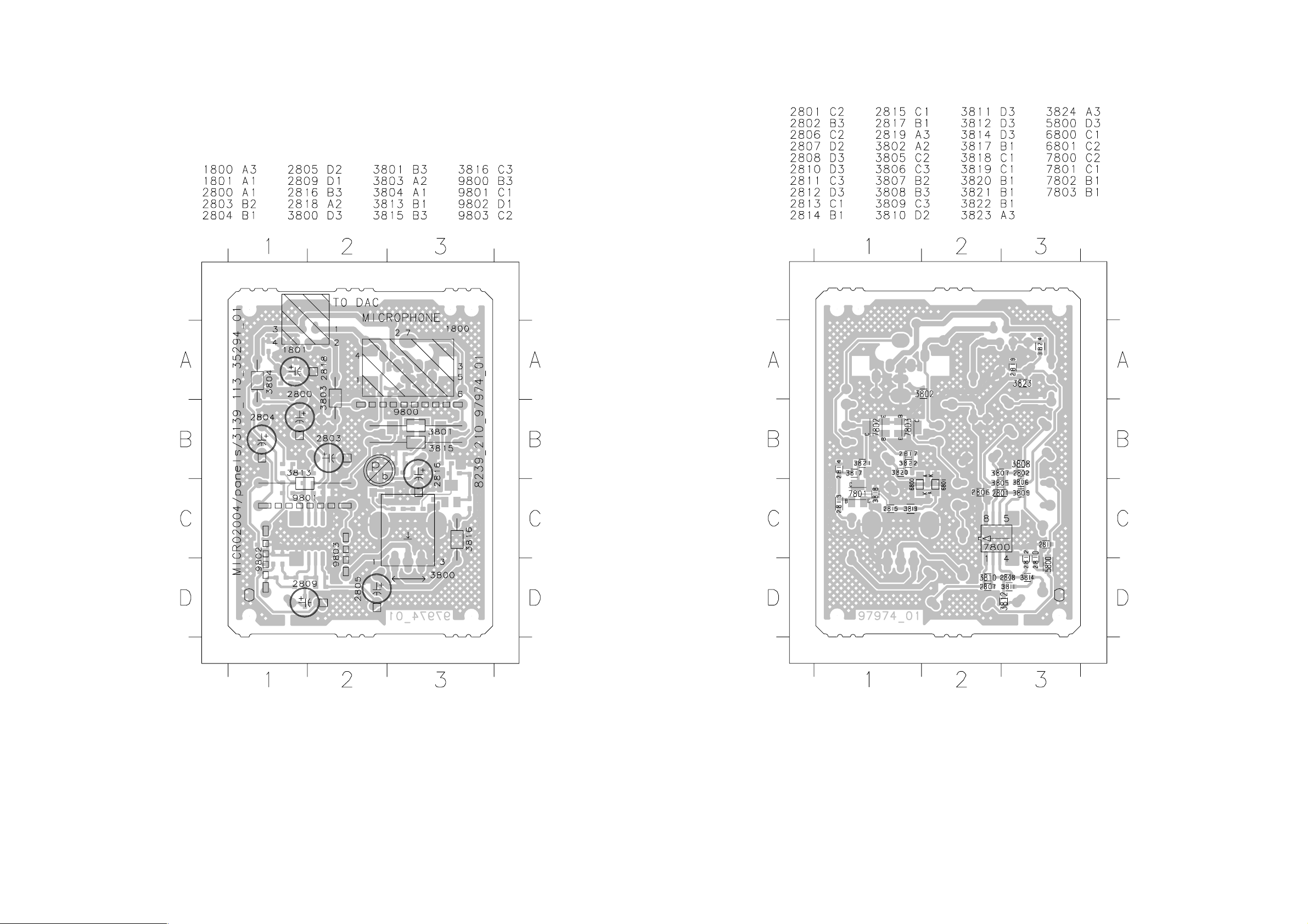
KARAOKE BOARD - COMPONENT LAYOUT (For MCD9 only)
This assembly drawing shows a summary of all possible versions.
For components used in a specific version see schematic diagram and respective parts list.
KARAOKE BOARD - CHIP LAYOUT (For MCD9 only)
This assembly drawing shows a summary of all possible versions.
For components used in a specific version see schematic diagram and respective parts list.
3139 113 3529 pt4 dd wk0409
3139 113 3529 pt4 dd wk0409

6-13
KARAOKE BOARD - CIRCUIT DIAGRAM (For MCD9 only)
6-13
A
B
C
D
1800 B1
1801 B9
2800 B7
2801 C7
2802 B6
2803 C6
2804 B6
2805 B5
2806 A5
2807 C4
2808 B4
2809 B3
2810 B3
2811 B2
2812 B2
2813 D5
2814 E4
2815 D4
1 23456789
ONLY USED FOR MCD9 VERSION
MIC IN
1800
TC38-103-61
Mic
4
2
7
1
6
3
5
3815
1K2
Mic
BC847B
7803
Vref
Mic
Mic
3814
12K
2812
100p
3813
2K2
+12V_A
BC847B
7802
2811
5800
22u
100p
Mic
2817
Mic
2809
100p
2810
MIC-ALC
1M
3822
100n
2816 E3
2817 E2
2818 E7
3802
50V22u
3820
150K
3821
560R
2816
3801
4K76K8
3812
5K6
2819 E6
3800 B5
3801 A3
+12V_A
6800
1SS355
50V10u
2808
3811
Vref
3819
6801
470p
6K8
2815
100n
3802 A3
3803 B9
3804 B8
3
2
1K
1SS355
+12V_A
8
4
Mic
3818
7800-A
NJM4560M
3810
270K
2807
47p
3817
1M
BC847B
7801
220R
3805 C7
3806 B6
3807 C6
2806
470n
1
1n
2814
2805
50V22u
2813
1u0
3808 B6
3809 C6
3810 C4
Mic
3816
3800
270R
3811 B4
3812 B3
3813 B2
20K
2
45
31
Mic
Vref
3814 A2
3815 B1
3816 D5
3817 D4
3818 E4
3819 D4
Microphone
Vref
2804
50V22u
3809
6K8
3808
Vref
3806
12K
2802
3807
2803
Mic
100p
1K2
50V1u0
5
6
3820 D3
3821 D3
3822 E3
+12V_A
8
4
2801
470p
3805
6K8
7800-B
NJM4560M
Mic
3823 E7
3824 E7
5800 B3
7
+12V_A
3823
2800
50V22u
4K7
6800 D3
6801 E4
7800-A B4
3804
1K0
7800-B B7
7801 D4
7802 D2
+12V_A
3803
470R
Mic
7803 D2
TO DAC
1801
1
2
3
4
FE-ST-VK-N
A
B
MIC_DET
+12V
MIC_OUT
GND_MIC
C
D
E
Note : Some values may varies, see respective parts list for correct value.
12
Mic
2819
22n
10V100u
2818
3824
4K7
Mic
8239_210_97974_01...for 3529 pt4 dd wk0409
3456789
E

6-14 6-14
ELECTRICAL PARTS LIST - FRONT BOARD
MISCELLANEOUS
1300 4822 265 11183 Flex Connector 4P
1301 2422 026 05563 Headphone Socket
1302 4822 265 10979 Flex Connector 15P
1303 4822 276 13775 Tact Switch
1304 4822 276 13775 Tact Switch
1305 4822 276 13775 Tact Switch
1306 4822 276 13775 Tact Switch
1307 4822 276 13775 Tact Switch
1308 4822 276 13775 Tact Switch
1309 4822 276 13775 Tact Switch
1310 4822 276 13775 Tact Switch
1311 4822 276 13775 Tact Switch
1312 2422 129 16708 Rotary Encoder 24P
1313 2422 129 00039 Rotary Encoder 24P
1314 2422 129 00039 Rotary Encoder 24P
1331 4822 276 13775 Tact Switch
1332 4822 276 13775 Tact Switch
1333 4822 276 13775 Tact Switch
1334 4822 276 13775 Tact Switch
1400 3139 110 53601 FTD HNA-13SM42
1401 4822 265 11545 Flex Connector 19P
1402 4822 265 11531 Flex Connector 9P
1405 4822 265 10979 Flex Connector 15P
1406 4822 265 11535 Flex Connector 8P
1407 4822 267 10956 Flex Connector 7P
1600 4822 265 11515 Flex Connector 8P
CAPACITORS
2300 2238 586 59812 100nF +80/-20% 50V
2301 2238 916 15641 22nF 10% 25V
2302 2238 916 15641 22nF 10% 25V
2303 9965 000 14169 100uF 10V 20%
2305 5322 126 11583 10nF 10% 50V
2306 5322 126 11583 10nF 10% 50V
2307 5322 126 11583 10nF 10% 50V
2308 5322 126 11583 10nF 10% 50V
2309 5322 126 11583 10nF 10% 50V
2310 5322 126 11583 10nF 10% 50V
2311 2238 586 59812 100nF +80/-20% 50V
2312 2238 586 59812 100nF +80/-20% 50V
2313 4822 126 11785 47pF 5% 50V
2314 4822 126 11785 47pF 5% 50V
2315 4822 126 11785 47pF 5% 50V
2401 3198 017 44740 470nF 10V
2402 5322 126 11583 10nF 10% 50V
2403 5322 126 11583 10nF 10% 50V
2404 3198 028 52290 22uF 20% 50V
2405 3198 028 52290 22uF 20% 50V
2407 2222 867 15339 33pF 5% 50V
2408 4822 122 33761 22pF 5% 50V
2409 4822 126 14223 2,2pF 50V
2410 4822 122 33761 22pF 5% 50V
2411 4822 122 33761 22pF 5% 50V
2412 2020 552 94427 100pF 5% 50V
2413 2020 552 94427 100pF 5% 50V
2414 2020 552 94427 100pF 5% 50V
2417 2020 552 94427 100pF 5% 50V
2418 2020 552 94427 100pF 5% 50V
2419 2020 552 94427 100pF 5% 50V
2420 2020 552 94427 100pF 5% 50V
2444 2238 586 59812 100nF +80/-20% 50V
2450 4822 124 81286 47uF 20% 16V
2451 2238 586 59812 100nF +80/-20% 50V
2453 4822 124 81286 47uF 20% 16V
2457 4822 124 81286 47uF 20% 16V
2460 2020 552 94427 100pF 5% 50V
2461 4822 124 12032 4,7uF 20% 50V
2462 4822 124 12032 4,7uF 20% 50V
2463 4822 124 12032 4,7uF 20% 50V
2464 4822 124 12032 4,7uF 20% 50V
2473 4822 124 12032 4,7uF 20% 50V
2474 4822 126 14238 2,2nF 50V
2480 2020 552 94427 100pF 5% 50V
2600 2238 586 59812 100nF +80/-20% 50V
2601 5322 126 11578 1nF 10% 50V /22/25
2602 4822 126 14249 560pF 10% 50V /22/25
2603 4822 126 14249 560pF 10% 50V /22/25
2604 4822 124 22652 2,2uF 20% 50V /22/25
2605 2238 586 59812 100nF +80/-20% 50V /22/25
2606 4822 126 11785 47pF 5% 50V /22/25
2607 4822 126 11785 47pF 5% 50V /22/25
RESISTORS
3301 4822 051 30151 150R 5% 0,062W
3302 4822 051 30221 220R 5% 0,062W
3303 4822 051 30271 270R 5% 0,062W
3304 4822 051 30391 390R 5% 0,062W
3305 4822 051 30561 560R 5% 0,062W
3306 4822 117 12968 820R 5% 0,62W
3307 4822 117 11817 1k2 1% 1/16W
3308 4822 117 12903 1k8 1% 0,063W
3312 4822 051 30103 10k 5% 0,062W
3313 4822 051 30103 10k 5% 0,062W
3314 4822 051 30103 10k 5% 0,062W
3315 4822 051 30103 10k 5% 0,062W
3316 4822 051 30103 10k 5% 0,062W
3317 4822 051 30103 10k 5% 0,062W
3318 4822 051 30103 10k 5% 0,062W
3319 4822 051 30103 10k 5% 0,062W
3320 4822 051 30103 10k 5% 0,062W
3321 4822 051 30103 10k 5% 0,062W
3323 4822 051 30152 1k5 5% 0,062W
ELECTRICAL PARTS LIST - FRONT BOARD
3324 4822 051 30152 1k5 5% 0,062W
3325 4822 051 30152 1k5 5% 0,062W
3326 4822 051 30152 1k5 5% 0,062W
3327 4822 051 30152 1k5 5% 0,062W
3328 4822 051 30152 1k5 5% 0,062W
3329 4822 051 30152 1k5 5% 0,062W
3330 4822 051 30152 1k5 5% 0,062W
3331 4822 051 30391 390R 5% 0,062W
3332 4822 051 30391 390R 5% 0,062W
3333 4822 051 30391 390R 5% 0,062W
3334 4822 051 30391 390R 5% 0,062W
3335 4822 051 30103 10k 5% 0,062W
3336 4822 051 30103 10k 5% 0,062W
3350 4822 051 30151 150R 5% 0,062W
3351 4822 051 30221 220R 5% 0,062W
3352 4822 051 30271 270R 5% 0,062W
3400 4822 117 12968 820R 5% 0,62W
3401 4822 117 12925 47k 1% 0,063W
3403 4822 117 13632 100k 1% 0,62W
3404 4822 051 30684 680k 5% 0,062W
3405 4822 051 30102 1k 5% 0,062W
3406 4822 117 12891 220k 1%
3407 4822 051 30102 1k 5% 0,062W
3408 4822 051 30102 1k 5% 0,062W
3409 4822 051 30102 1k 5% 0,062W
3410 4822 051 30102 1k 5% 0,062W
3411 4822 051 30102 1k 5% 0,062W
3412 4822 051 30102 1k 5% 0,062W
3413 4822 051 30103 10k 5% 0,062W
3414 4822 051 30103 10k 5% 0,062W
3415 4822 051 30102 1k 5% 0,062W
3416 4822 051 30102 1k 5% 0,062W
3417 4822 051 30102 1k 5% 0,062W
3418 4822 051 30102 1k 5% 0,062W
3419 4822 051 30102 1k 5% 0,062W
3420 4822 050 21003 10k 1% 0,6W
3421 4822 051 30103 10k 5% 0,062W
3422 4822 051 30102 1k 5% 0,062W
3423 4822 051 30102 1k 5% 0,062W
3424 4822 051 30102 1k 5% 0,062W
3425 4822 051 30102 1k 5% 0,062W
3426 4822 051 30102 1k 5% 0,062W
3427 4822 051 30102 1k 5% 0,062W
3428 4822 051 30102 1k 5% 0,062W
3431 4822 051 30102 1k 5% 0,062W
3432 4822 051 30472 4k7 5% 0,062W
3433 4822 116 52263 2k7 5% 0,5W
3434 4822 116 83883 470R 5% 0,5W
3435 4822 051 30102 1k 5% 0,062W /22/25
3436 3198 021 32250 RST SM 0603 2M2 5%
3439 4822 051 30102 1k 5% 0,062W
3440 4822 051 30102 1k 5% 0,062W
3441 4822 051 30102 1k 5% 0,062W
3442 4822 051 30101 100R 5% 0,062W
3443 4822 051 30101 100R 5% 0,062W
3444 4822 051 30102 1k 5% 0,062W
3445 4822 051 30102 1k 5% 0,062W
3446 4822 051 30471 470R 5% 0,062W
3447 4822 051 30471 470R 5% 0,062W
3448 4822 051 30471 470R 5% 0,062W
3452 4822 051 30471 470R 5% 0,062W
3453 4822 051 30102 1k 5% 0,062W
3454 4822 051 30102 1k 5% 0,062W
3455 4822 051 30102 1k 5% 0,062W
3456 4822 051 30102 1k 5% 0,062W
3457 4822 051 30102 1k 5% 0,062W
3458 4822 051 30102 1k 5% 0,062W
3459 4822 051 30102 1k 5% 0,062W
3460 4822 051 30102 1k 5% 0,062W
3461 4822 051 30102 1k 5% 0,062W
3462 4822 051 30102 1k 5% 0,062W
3463 4822 051 30471 470R 5% 0,062W
3464 4822 051 30471 470R 5% 0,062W
3465 4822 051 30272 2k7 5% 0,062W
3466 4822 051 30102 1k 5% 0,062W
3467 4822 051 30102 1k 5% 0,062W
3468 4822 051 30102 1k 5% 0,062W
3469 4822 051 30102 1k 5% 0,062W
3470 4822 051 30102 1k 5% 0,062W
3471 4822 051 30102 1k 5% 0,062W
3472 4822 051 30102 1k 5% 0,062W
3473 4822 051 30102 1k 5% 0,062W
3474 4822 051 30102 1k 5% 0,062W
3475 4822 051 30102 1k 5% 0,062W
3476 4822 051 30102 1k 5% 0,062W
3477 4822 051 30102 1k 5% 0,062W
3478 4822 051 30102 1k 5% 0,062W
3479 4822 051 30102 1k 5% 0,062W
3480 4822 051 30102 1k 5% 0,062W
3481 4822 051 30102 1k 5% 0,062W
3482 4822 051 30102 1k 5% 0,062W
3483 4822 051 30102 1k 5% 0,062W
3484 4822 051 30102 1k 5% 0,062W
3485 4822 051 30102 1k 5% 0,062W
3486 4822 051 30102 1k 5% 0,062W
3487 4822 051 30102 1k 5% 0,062W
3488 4822 051 30102 1k 5% 0,062W
3489 4822 051 30102 1k 5% 0,062W
3490 4822 117 12864 82k 5% 0,6W
3491 4822 051 30103 10k 5% 0,062W
3492 4822 117 12864 82k 5% 0,6W
3493 4822 117 12864 82k 5% 0,6W

6-15 6-15
ELECTRICAL PARTS LIST - FRONT BOARD ELECTRICAL PARTS LIST - FRONT BOARD
RESISTORS
3494 4822 051 30682 6k8 5% 0,062W
3495 4822 051 30682 6k8 5% 0,062W
3496 4822 051 30103 10k 5% 0,062W /21
3497 4822 050 21003 10k 1% 0,6W /21
3498 4822 051 30101 100R 5% 0,062W
3499 4822 051 30101 100R 5% 0,062W
3500 4822 051 30221 220R 5% 0,062W
3501 4822 051 30221 220R 5% 0,062W
3502 4822 051 30471 470R 5% 0,062W
3509 4822 051 30103 10k 5% 0,062W
3510 4822 051 30103 10k 5% 0,062W
3511 4822 051 30103 10k 5% 0,062W
3513 4822 051 30102 1k 5% 0,062W
3514 4822 051 30102 1k 5% 0,062W
3515 4822 051 30102 1k 5% 0,062W
3518 4822 116 83872 220R 5% 0,5W
3519 4822 116 80176 1R 5% 0,5W
3520 4822 116 80176 1R 5% 0,5W
3521 4822 116 52257 22k 5% 0,5W
3522 4822 116 83872 220R 5% 0,5W
3523 4822 116 80176 1R 5% 0,5W
3524 4822 116 80176 1R 5% 0,5W
3527 4822 051 30101 100R 5% 0,062W
3529 4822 051 30101 100R 5% 0,062W
3531 4822 051 30101 100R 5% 0,062W
3532 4822 051 30101 100R 5% 0,062W
3533 4822 051 30103 10k 5% 0,062W
3534 4822 051 30102 1k 5% 0,062W
3535 4822 116 52263 2k7 5% 0,5W
3600 4822 051 30102 1k 5% 0,062W
3601 4822 051 30102 1k 5% 0,062W
3602 4822 051 30103 10k 5% 0,062W /22/25
3603 4822 116 52243 1k5 5% 0,5W /22/25
3604 4822 117 12891 220k 1% /22/25
3605 4822 051 30222 2k2 5% 0,062W /22/25
3606 4822 050 11002 1k 1% 0,4W /22/25
3607 4822 050 11002 1k 1% 0,4W /22/25
4300 4822 051 30008 0R Jumper 0603
4301 4822 051 30008 0R Jumper 0603
4302 4822 051 30008 0R Jumper 0603
4303 4822 051 30008 0R Jumper 0603
4310 4822 051 30008 0R Jumper 0603
4311 4822 051 30008 0R Jumper 0603
4312 4822 051 30008 0R Jumper 0603
4313 4822 051 30008 0R Jumper 0603
4314 4822 051 30008 0R Jumper 0603
4315 4822 051 30008 0R Jumper 0603
4316 4822 051 30008 0R Jumper 0603
4400 4822 051 30008 0R Jumper 0603
4404 4822 051 30008 0R Jumper 0603
4405 4822 051 30008 0R Jumper 0603
4406 4822 051 30008 0R Jumper 0603
4407 4822 051 30008 0R Jumper 0603
4409 4822 051 30008 0R Jumper 0603
4411 4822 051 30008 0R Jumper 0603
4420 4822 051 30008 0R Jumper 0603
4421 4822 051 30008 0R Jumper 0603
4423 4822 051 30008 0R Jumper 0603
4424 4822 051 30008 0R Jumper 0603
4426 4822 051 30008 0R Jumper 0603
4427 4822 051 30008 0R Jumper 0603
4430 4822 051 30008 0R Jumper 0603
4431 4822 051 30008 0R Jumper 0603
4432 4822 051 30008 0R Jumper 0603
4433 4822 051 30008 0R Jumper 0603
4434 4822 051 30008 0R Jumper 0603
4436 4822 051 30008 0R Jumper 0603
4437 4822 051 30008 0R Jumper 0603
4438 4822 051 30008 0R Jumper 0603 /22/25
4439 4822 051 30008 0R Jumper 0603
4440 4822 051 30008 0R Jumper 0603
4441 4822 051 30008 0R Jumper 0603
4442 4822 051 30008 0R Jumper 0603
4443 4822 051 30008 0R Jumper 0603
4444 4822 051 30008 0R Jumper 0603
4445 4822 051 30008 0R Jumper 0603
4446 4822 051 30008 0R Jumper 0603
4447 4822 051 30008 0R Jumper 0603
4448 4822 051 30008 0R Jumper 0603
4449 4822 051 30008 0R Jumper 0603
4450 4822 051 30008 0R Jumper 0603
4451 4822 051 30008 0R Jumper 0603
4452 4822 051 30008 0R Jumper 0603
4453 4822 051 30008 0R Jumper 0603
4454 4822 051 30008 0R Jumper 0603
4455 4822 051 30008 0R Jumper 0603
4456 4822 051 30008 0R Jumper 0603
4457 4822 051 30008 0R Jumper 0603 /22/25
4458 4822 051 30008 0R Jumper 0603
COILS & FILTERS
5300 3198 018 52280 FXDIND SM 0603 2U2 10%
5301 3198 018 52280 FXDIND SM 0603 2U2 10%
5302 3198 018 52280 FXDIND SM 0603 2U2 10%
5303 3198 018 54780 FXDIND SM 0603 4U7 10%
5304 3198 018 54780 FXDIND SM 0603 4U7 10%
5400 5322 242 73686 RES CER 12MHz
5401 2422 543 01069 RES XTL 32,768kHz
5402 3198 018 54780 FXDIND SM 0603 4U7 10%
5403 3198 018 54780 FXDIND SM 0603 4U7 10%
5404 4822 157 62552 Coil 2,2uH 5%
5405 4822 157 62552 Coil 2,2uH 5%
5406 4822 157 62552 Coil 2,2uH 5%
5407 4822 157 62552 Coil 2,2uH 5%
5600 3198 018 52280 FXDIND SM 0603 2U2 10%
5601 3198 018 52280 FXDIND SM 0603 2U2 10% /22/25
5602 4822 242 11033 RES XTL 4,332MHz /22/25
DIODES
6300 9322 190 55676 LED VS LTL-816TDK3
6301 9322 190 55676 LED VS LTL-816TDK3
6302 9322 190 55676 LED VS LTL-816TDK3
6303 9322 190 55676 LED VS LTL-816TDK3
6304 9322 190 55676 LED VS LTL-816TDK3
6305 9322 190 55676 LED VS LTL-816TDK3
6306 9322 179 76676 LED VS LTL-816EELC
6308 4822 130 31878 1N4003G
6309 4822 130 11397 BAS316
6400 4822 130 30621 1N4148
6401 4822 130 30621 1N4148
6402 4822 130 30621 1N4148
6403 4822 130 30621 1N4148
6404 4822 130 30621 1N4148
6405 4822 130 31878 1N4003G
6406 4822 130 31878 1N4003G
6407 4822 130 31878 1N4003G
6408 4822 130 30621 1N4148
6409 4822 130 34278 BZX79-B6V8
6410 4822 130 30621 1N4148
TRANSISTORS & INTEGRATED CIRCUITS
7301 4822 209 15449 IC SM 74HC4094D
7302 5322 130 60159 BC847B
7400 3139 110 53741 TMP88CU74YF - 'MCM7/8S53741'
7401 4822 130 60373 BC857B
7402 5322 130 60159 BC847B
7403 9322 185 95667 IR Receiver TSOP4836ZC1
7404 5322 130 60159 BC847B
7405 5322 130 60159 BC847B
7407 5322 130 60159 BC847B
7408 5322 130 60159 BC847B
7600 9322 145 26668 IC SM M24C02-WMN6
7601 9352 686 05118 IC SM SAA6581T /22/25
Note : Only the parts mentioned in this list are normal service
spare parts.

7A-17A-1
1
FM
Osc.
FM
Mixer
AM
Mixer
AM
Osc.
AM IF
IF1
IF2
FM
Det.
AM
Det.
3393733
RADIO IC
TEA 5757H
TUNER BOARD
ECO 6
Systems
1018 11
14
15
24
right
right
left
left
stereo
VCO
4140 36 193244 25
Stereo
Decoder
AFC
AFC +
AFC -
4
4
AGC
Pre-
scaler
Multi-
plexer
Charge
pump
Stabilizer
CONTROL
Reference
Oscillator
29
28
27
clock
data
enable
P1
P0
31
30
programmable
output ports
V
Loop
V
Loop
V
Loop
V
Loop
V
Loop
2
6
5
43
C
D
450kHz450kHz450kHz
20
75kHz
V
Stab
AV
Stab
BV
Stab
B
V
Stab
A V
Stab
B
10,7 MHz 10,7 MHz
35 9
Vdd Vcc1
723
V
Stab
A
V
Stab
B
38
34
22
Vcc2
8
ECO6 Systems, 140499
LF filter
RDS
(MPX)
RDS
(MPX)
stereo
clock
data
enable
Version
1120
1
8
FM
Frontend
AM
Frontend
AM-FRAME AERIAL
B
1103
1101
(1102)
A
FM
MPX
buffer ampl.
5
Discriminator
10,7 MHz
Vdd
Vcc1
Vcc
Vcc2
AM-RF
AM-Osc.
FM-Osc.
FM-RF FM-IF 1 FM-IF 2
AM-IF 1 AM-IF 2
AM-AFC
3
2
BLOCK DIAGRAM
ECO6 Tuner Board
version:
SYSTEMS non-CENELEC
TABLE OF CONTENTS
Blockdiagram ..................................................................7A-1
Schematic Diagram.........................................................7A-2
Component Layout..........................................................7A-3
Adjustment table .............................................................7A-3
Electrical Partslist............................................................7A-4

7A-2 7A-2
ECO6 Sys-non Cenelec, 000911
1101 A1
1102 B1
1103 F2
1120 E14
1130 A2
1131 B2
1132 G13
2101 B3
2102 B1
2103 C7
2104 B3
2105 A2
2106 F3
2107 F4
2119 H6
2120 G6
2124 H6
2125 H6
2126 F7
2127 E7
2128 C8
2129 C7
2130 F11
2131 G8
2132 G8
2133 G8
2134 H8
2135 H9
2136 G14
2137 G13
2138 F9
2139 G9
2140 G9
2141 F10
2143 G12
2144 G11
2145 F12
2146 E12
2147 E12
2148 E12
2149 H7
2150 A10
2152 E4
2153 E5
2154 D5
2155 D5
2159 F6
2161 C11
2163 D11
2164 F10
2165 C7
2166 E11
2167 E11
2169 H8
3101 E4
3102 D4
3103 C6
3104 A7
3105 B6
3132 G5
3134 H6
3141 E7
3142 E7
3143 G7
3144 H7
3145 F8
3146 G13
3152 G14
3153 G13
3154 G13
3155 G11
3156 C12
3157 C12
3158 E13
3159 D13
3160 D12
3161 D13
3167 F12
3168 F11
3169 E11
3170 C12
3172 G12
3176 G7
3181 E6
5102 F2
5109 B9
5110 B10
5111 A8
5112 A11
5114 B11
5119 G9
5121 E11
5123 G5
5130 E5
5131 C6
6103 B2
6105-1 F3
6105-2 G5
6106 C3
6107 G13
6120 C13
6130 E5
6131 D5
7101 C8
7102 C6
7103 H7
7111 C13
7112 G12
T102 B2
T103 B2
T105 F2
T106 F2
T109 B6
T110 F5
T111 F4
T112 F7
T113 A8
T114 B10
T115 A8
T116 F10
T117 G13
T118 G11
T120 F13
T121 F13
T122 F13
T123 E13
T124 G14
T125 F14
T126 F13
T127 F13
T128 D7
T140 F11
T141 F10
T142 F10
1
34
6
87
2
1
34
6
87
2
LEGEND
p ...for provision only
USA ... for USA version only
E-EU ... for East European version only
22n
USA
22n
USA
p
p
p
7
1
2
3
8
6105
6
HN1V02H
54
3
6
1
2
7
29
25
13
30
31
16
4
42
15
1
7
22
9
23
38 34
2118
37 35
33
43 39
5
3
8
171412
24
11
10
2019
44
32
41 3640
6
2
27
28
26
1
3
4
5
6
87
2
1
34
6
87
2
1
34
6
87
2
p
SCALER
MULTIPLEXER
CONTROL
FILTER
AM
IF
AM
DET
FM
DET
VSTABB
DECODER
CHARGE
PUMP
AGC
OSC
AM DET
FM
IF2
RIPPLE
AGC
STABILIZER
AFC
VDD
VSTABA
AM-IF
MONO/
FM
FRONTEND
CONTROL
XTAL
AGC
PRE-
CTRL
AGC
AM
OSC
AGC
VCC2
FM
OSC
AM
MIXER
MIXER
FM
FM
IF1
FRONTEND
AM
STEREO
STEREO
RDS only
DISCRIMINATOR
to/from
FM-OSCILLATOR
PROGR.
MPX
Q-multiplier
MW
OUTPUT PORTS
to 1120
pin 5
ENABLE/MPX
BUFFER
kHz
VERSION DETECTION
VCO
RIGHT
14
12 3
AM FRAME AERIAL
DATA
C
D
E
F
AM-OSCILLATOR
FM 75 OHM
FM-IF2
MW
2345
AM-RF
450kHz
450kHz
AM-IF2
from 2169
78
AM-AFC
LEFT
6 7 8 9 10 11 12 13
456
FM-RF
TUNER BOARD ECO6
/ SYSTEMS NON CENELEC
9 1011121314
A
B
G
H
A
B
1
VCC
STEREO
CLOCK
AMPLIFIER
GND
H
C
D
E
F
G
470n
2132
BAS216
6120
2103
1u
2107
1n
3134
22K
6105-2
HN1V02H
100n
2163
T141
7KL
1K
3144
5102
3157
100K
T109
470R
3153
2130
22n
220R
3105
3142
100K
3167
120R
33p
2149
2K2
3145
1132
C-PAD
T103
T111
2164
470n
T102
2140 15p
2139
2138
2u2
82p
2133
1u
3103
8K2
T120
4p7
2154
3156
1101
USA
YKD21
100K
2161
100n
5119
2119
10p
T142
5123
11p
2106
3172
6106
BAS216
100n
2165
5K6
3154
3155
220R
330R
2124
33K
3176
22n
WRITE-EN
5114
7P
MUTE
P0
P1
PILOT
RF-GND1
RF-GND2
RIGHT
RIPPLE
VCC1
VCC2
VCO
VDD
VSTABA
VSTABB
FM-DEMOD
FM-IF1-IN
FM-IF2
FM-IF2-IN
FM-IN
FM-MIXOUT
FM-OSC
FM-RF
I-TUNE
IF-GND
LEFT
LPF
MPX-IN
AF-OUT
AFC+
AFC-
AGC
AM-AFC
AM-IF1-IN
AM-IF2
AM-MIXOUT
AM-OSC
AM-RF
CLOCK
DATA
DIG-GND
FIELDSTR-IND
5130
T127
T126
220n
2127
5121
DT-381
150K
3169
75K
3102
100K
56K
3141
1131
C-PAD
3132
5112
7P
6107
47R
6131
1SV228
BZX284-C11
1120
FE-BT-VK-N
T118
T140
T117
T112
2131
470n
33K
3101
1SV228
6130
3168
120R
2125
560p
T116
2n2
2148
100n
2141
470R
18p
2120
470R
3158
3152
3159
XH-S
1103
3160
470R
470R
220n
2143
2150
T125
1
2
3
4
5
6
7
8
22R
3146
BF550
7102
5131
11p
2155
O
100K
5110
G
I
1102
not USA
3170
T122
2135
15n
2167
2145
220p
T110
12p
HN1V02H
1n
2166
T105
6105-1
T106
T121
T123
BC547C
7112
3143
2129
100u
C-PAD
1130
22K
220n
2137
T128
3181
1K
330p
2126
2101
47p
BAV99
6103
2104
100p
2153
15p
T124
2152
33n
560p
E-EU
12p
E-EU
2p2
J
33p
2159
220p
2146
2169
2n2
1u
15n
2134
2144
220n
2136
22K
3161
BC857C
BC847C
7111
7103
2147
220p
VCC2
VCC2
VDD
T114
MPX
P1
P0
P1
VDD
MPX
VCC1
VCC1
VCC1
printed
printed
printed
1
2
13
2
1
2
3
1
2
TEA5757H
TEA5759H
J
7101
2128
10u
7111
component mounted
/14 FM-OIRT/MW
/00 /02 FM/MW/LW
6120 3170
/01 FM/MW
VERSION
/00 /02 FM/MW
3156
/17 FM/AM
/06 FM-Japan/AM
3157
VERSION PROGRAMMING COMPONENTS
J ... for Japanese version only
AM-IF1
450kHz
8
5111
1
2
3
4
6
7
T113
T115
FM-IF1
2
G
1I3
O
5109
3104
330R
100n
0R
4103
...V MW mode
...V LW mode
voltages measured while
set is tuned to a strong transmitter
...V FM mode stereo
EVM
V
5V
0V
152kHz, 50mV
pp
stereo stereomono
9.6V
9.5V
9.5V
10.4V
12V
1V
1.3V
1.4V
stereo 0.2V
mono 4.8V
9.6V
12Vtyp
stereo 0.4V
0.15V
11.1V
7.8V
2V
0.7V
0V
1.2V
7.6V
(10-14V)
0.2V
0V
1.2V
0.1V
D
1.4V
0.7V
4
0V
0V
mono 4.8V
1.4V
9.6V
1.4V
0.2V
0.7V
1.4V
7.9V
7.7V
0V
0V
0V
0V
0.6V
0.8V
0.1V
1.6-8V
1-8V
11.1V
0V
1V
1.4V
1.4V
B
7.6V
5
3
2
A
1.3V
0.7V
7.8V
11.1V
0.8V
0.6V
0.6V
1V
0.7V
1V
1.1V
1.1V
0V
0V
2V
C
1
0.8V
1.2V
1.1V
IF-AMP.
BFS20
7119
J
1K
3113
J
2112
J
100p
330R
3119
J
Signal path
FM
AF - left/right
AM
MPX (Audio Frequency)
2102
100n
2105
USA
100n

7A-37A-3
VARICAP ALIGNMENT
FM RF
FM IF
VCO
AM IF
AM RF
3)
108MHz
87.5MHz
(65.81MHz)
87.5MHz
(65.81MHz)
87.5MHz
(65.81MHz)
279kHz
153kHz
1602kHz
531kHz
5130
check
5122
check
5123
check
8V ±0.2V
4.3V ±0.5V
(1.2V ±0.5V)
8V ±0.2V
1.1V ±0.4V
8V ±0.2V
1.1V ±0.4V
1494kHz
558kHz
560kHz 5102
1500kHz
5103198kHz
1494kHz
558kHz
560kHz
1500kHz
198kHz
2106
5102
2106
3142 152kHz ±1kHz
1)
98MHz
5112
MAX
FM
87.5 - 108MHz
(65.81 - 74, 87.5 - 108MHz)
LW
153 - 279kHz
MW
FM/MW/LW- version, 9kHz grid
531 - 1602kHz
1700kHz
530kHz
5123
check
8V ±0.2V
1.1V ±0.4V
1602kHz
531kHz
5123
check
6.9V ±0.2V
1.1V ±0.4V
108MHz
108MHz 2155
5131
MW
FM/AM-version, 10kHz grid
530 - 1700kHz
FM
MW
LW
98MHz, 1mV
continuous wave
450kHz
connect pin 6 of
IC 7101 (AM Osc.)
with 3.3kΩ to Vcc
Use Service Testprogram. By selecting the TUNER TEST test frequencies will be stored as preset frequencies automatically.
4
1
3
5
5
A
A
5119FM
10.7MHz, 45mV
continuous wave
2D
mod=1kHz
∆f=±22.5kHz
1)
If sensitivity of frequency counter is too low adjust to max. channel separation
(input signal: stereo left 90% + 9%, adjust output on right channel to minimum)
Repeat
ECO6, Sys + PA with frame aerial, 070799
TUNER ADJUSTMENT TABLE ( ECO6 FM/MW- and FM/MW/LW - versions with AM-frame aerial )
∆f=±10kHz
VRF = 0.5mV
C
see
remark
2)
220R
100nF
36
IC 7101
220R
100nF
40
IC 7101
2141
shortcircuit
to block AFC
21
IC 7101
max.
symmetric
f
o
AM AFC
MW
C
continuous wave
VRF = 2mV
5111
5114
2
0 ± 2 mV DC
0 ± 3 mV DC
MW
4)
FM/MW/LW- and FM/MW-version
( 9kHz grid)
531 - 1602kHz
B
∆f = ±30kHz
V
RF
as low as
possible
max.
symmetric
f
o
MW
FM/AM-version, 10kHz grid
530 - 1700kHz
3)
For AM RF adjustments the original frame antenna has to be used !
2)
RC network serves for damping the IF-filter while adjusting the other one.
4)
MW has to be aligned before LW.
Waverange Input frequency Input Tuned to Adjust Output Scope/Voltmeter
FM
87.5 - 108MHz
(65.81 - 74, 87.5 - 108MHz)
FM/MW-version, 9kHz grid
531 - 1602kHz
(as low as
possible)
ECO6 System non Cenelec stage .3, 120900
TUNER BOARD ECO6
Systems non Cenelec
/ componentside view
1101 A6
1102 B6
1103 D6
1120 A4
1130 B5
1131 D5
1132 A5
2106 C5
2107 B5
2128 C4
2129 B4
2133 D2
2138 C2
2144 B2
2155 C4
3142 D2
5102 D6
5109 A3
5110 B3
5111 B4
5112 A3
5114 A2
5119 C2
5121 B2
5123 D5
5130 D3
5131 D4
7112 C1
9101 A2
9103 B2
9104 B5
9105 B1
9106 B3
9107 D4
9108 C4
9109 D2
AM FRAME AERIAL
FM 75Ω
B
A
TUNER BOARD ECO6
Systems - non Cenelec
/
copperside view
2101 B4
2102 B1
2103 D4
2104 B4
2105 C1
2112 B5
2119 D3
2120 D3
2124 D3
2125 D3
2126 D6
2127 C5
2130 D5
2131 C5
2132 D6
2134 D7
2135 D7
2136 A4
2137 A4
2139 C6
2140 C6
2141 C6
2143 C7
2145 A5
2146 B7
2147 A5
2148 B6
2149 D6
2150 B5
2152 C5
2153 C5
2154 C4
2159 C5
2161 A6
2163 B6
2164 C6
2165 C4
2166 B6
2167 B6
2169 A4
3101 D5
3102 C3
3103 C4
3104 B4
3105 C4
3113 B5
3119 B5
3132 D5
3134 D3
3141 C5
3143 D6
3144 B7
3145 C5
3146 C7
3152 A4
3153 A4
3154 C7
3155 C7
3156 A6
3157 A6
3158 A4
3159 A5
3160 A5
3161 A5
3167 B7
3168 C7
3169 B6
3170 A6
3172 C7
3176 D6
3181 D4
4103 B5
4106 C4
4107 C5
4108 C5
6103 B3
6105 C3
6106 C3
6107 C7
6120 A6
6130 D4
6131 C4
7101 C5
7102 D4
7103 D7
7111 A5
7119 B5
These assembly drawings show a summary of all possible versions.
For components used in a specific version see schematic diagram respectively partslist.
ECO6 Systems non CENELEC stage .3, 120900
41..
in schematic diagram)
(not all items shown
SMD jumper
EB
C
A
K
1
2
7
8
4
D
A
C
1
2
5
3
V
dd
Vcc2
Vcc1

MISCELLANEOUS
–––––––––––––––––––––––––––––––––––––––––––––––––––––
1101 2422 015 19376 SOCKET 2P CLICKFIT USA only
1102 4822 267 10283 SOCKET COAX, IEC 75Ω not USA
1103 4822 265 31184 JST CONNECTOR 2 POLE
1120 4822 265 11515 FFC SOCKET, 8P
CAPACITORS
–––––––––––––––––––––––––––––––––––––––––––––––––––––
2101© 4822 126 13692 47pF 1% 63V
2102© 4822 126 13838 100nF 10% 50V not USA
2103© 5322 122 31647 1nF 10% 63V
2104© 5322 122 32531 100pF 5% 50V
2105© 4822 126 13838 100nF 10% 50V USA only
2106 2020 800 00191 3-11pF TRIMCAP.,N450
2107 4822 121 51319 1µF 20% 50V
2120© 4822 126 13689 18pF 1% 63V
2124© 5322 122 32654 22nF 10% 63V
2125© 2020 552 96199 560pF 1% 50V
2126© 5322 122 31863 330pF 5% 50V
2127© 4822 126 14076 220nF 20% 25V
2128 4822 124 40248 10µF 20% 63V
2129 4822 124 41584 100µF 20% 10V
2130© 5322 122 32654 22nF 10% 63V
2131© 4822 126 13482 470nF 20% 16V
2132© 4822 126 13482 470nF 20% 16V
2133 4822 124 21913 1µF 20% 63V
2134© 4822 126 13188 15nF 5% 63V not USA
2134© 5322 122 32654 22nF 10% 63V USA only
2135© 4822 126 13188 15nF 5% 63V not USA
2135© 5322 122 32654 22nF 10% 63V USA only
2136© 4822 126 14076 220nF 20% 25V
2137© 4822 126 14076 220nF 20% 25V
2138 4822 124 22652 2,2µF 20% 50V
2139© 4822 126 14236 15pF 5% 50V
2140© 4822 126 13695 82pF 1% 63V
2141© 4822 126 13838 100nF 10% 50V
2143© 4822 126 14076 220nF 20% 25V
2144 4822 124 21913 1µF 20% 63V
2145© 4822 122 33575 220pF 5% 50V
2146© 4822 122 33575 220pF 5% 50V
2147© 4822 122 33575 220pF 5% 50V
2148© 4822 122 33127 2,2nF 10% 63V
2149© 5322 122 32659 33pF 5% 50V RDS only
2150© 4822 126 13838 100nF 10% 50V
2152© 4822 126 12105 33nF 5% 63V not for East Europe
2152© 5322 116 80853 560pF 5% 63V for East Europe only
2153© 4822 126 13486 15pF 2% 63V not for East Europe
2153© 4822 122 33926 12pF 2% 50V for East Europe only
2155 2020 800 00191 3-11pF TRIMCAP.,N450
2159© 5322 122 32659 33pF 5% 50V
2164© 4822 126 13482 470nF 20% 16V
2165© 4822 126 13838 100nF 10% 50V
2166© 5322 122 31647 1nF 10% 63V
2167© 4822 122 33926 12pF 5% 50V
2169© 4822 122 33127 2,2nF 10% 63V RDS only
RESISTORS
–––––––––––––––––––––––––––––––––––––––––––––––––––––
3101© 4822 051 20333 33kΩ 5% 0,1W
3102© 4822 117 10837 100kΩ 1% 0,1W
3103© 4822 051 20822 8,2kΩ 5% 0,1W
3104© 4822 117 13577 330Ω 1% 0,1W
3105© 4822 117 11503 220Ω 5% 0,1W
3132© 4822 051 20479 47Ω 5% 0,1W
3134© 4822 051 20223 22kΩ 5% 0,1W
3141© 4822 117 11148 56kΩ 1% 0,1W
3142 4822 100 12159 TRIMPOT. 100kΩ
RESISTORS
–––––––––––––––––––––––––––––––––––––––––––––––––––––
3143© 4822 051 20223 22kΩ 5% 0,1W RDS only
3144© 4822 051 10102 1kΩ 2% 0,25W RDS only
3145© 4822 117 11449 2,2kΩ 1% 0,1W
3146© 4822 051 20229 22Ω 5% 0,1W
3152© 4822 051 20471 470Ω 5% 0,1W
3153© 4822 051 20471 470Ω 5% 0,1W
3154© 4822 117 13577 330Ω 1% 0,1W
3155© 4822 117 11503 220Ω 5% 0,1W
3156© 4822 117 10837 100kΩ 1% 0,1W
3157© 4822 117 10837 100kΩ 1% 0,1W
3158© 4822 051 20471 470Ω 5% 0,1W
3159© 4822 051 20471 470Ω 5% 0,1W
3160© 4822 051 20471 470Ω 5% 0,1W
3161© 4822 051 20223 22kΩ 5% 0,1W
3167© 4822 051 20121 120Ω 5% 0,1W
3168© 4822 051 20121 120Ω 5% 0,1W
3169© 4822 051 20154 150kΩ 5% 0,1W
3170© 4822 117 10837 100kΩ 1% 0,1W
3172© 4822 051 20562 5,6kΩ 5% 0,1W
3176© 4822 051 20333 33kΩ 5% 0,1W RDS only
3181© 4822 051 10102 1kΩ 2% 0,25W
4103© 4822 051 20008 CHIP JUMPER 0805
4106© 4822 051 20008 CHIP JUMPER 0805
4107© 4822 051 20008 CHIP JUMPER 0805
4108© 4822 051 20008 CHIP JUMPER 0805
COILS
–––––––––––––––––––––––––––––––––––––––––––––––––––––
5102 4822 157 71634 RF-COIL MW
5109 4822 242 70665 FM-IF FILTER 10,7MHz
5110 4822 242 70665 FM-IF FILTER 10,7MHz
5111 2422 549 44023 AM-IF FILTER 450kHz
5112 4822 157 70302 AM-IF FILTER 450kHz
5114 4822 157 70302 AM-IF FILTER 450kHz
5119 4822 157 11443 DISCRIMINATOR COIL
5121 4822 242 10261 QUARTZ 75kHz
5123 2422 549 44108 RF-COIL, AM-OSCILLATOR
5130 4822 157 11843 RF COIL 1,5 TURNS
5131 4822 157 11843 RF COIL 1,5 TURNS
DIODES
–––––––––––––––––––––––––––––––––––––––––––––––––––––
6103© 5322 130 34337 BAV99
6105© 4822 130 83075 HN1V02H
6106© 4822 130 83757 BAS216
6107© 9340 386 90115 BZX284-C11
6120© 4822 130 83757 BAS216
6130© 4822 130 82833 1SV228
6131© 4822 130 82833 1SV228
TRANSISTORS
–––––––––––––––––––––––––––––––––––––––––––––––––––––
7102 4822 130 42131 BF550
7103© 5322 130 42756 BC857C RDS only
7111© 5322 130 42755 BC847C
7112 4822 130 44503 BC547C
INTEGRATED CIRCUITS
–––––––––––––––––––––––––––––––––––––––––––––––––––––
7101© 9351 740 80557 TEA5757H/V1, RADIO IC
7A-4
Electrical Partslist
ECO6
SYSTEMS NON-CENELEC
7A-4

7B-1 7B-1
1
AM
Mixer
AM
Osc.
AM IF
IF1
IF2
FM
Det.
AM
Det.
37 33
RADIO IC
TEA 5762
TUNER BOARD
ECO 6
Systems Cenelec
1018 11
143915
24
right
AM/FM
right
left
left
stereo
VCO
4140 36 193244 25
Stereo
Decoder
AFC
AFC +
AFC -
4
4
AGC
Pre-
scaler
Multi-
plexer
Charge
pump
Stabilizer
CONTROL
Reference
Oscillator
292827
clock
data
enable
P1
P0
31
30
programmable
output ports
V
Loop
V
Loop
V
Loop
2
6
5 FM Osc.
C
D
450kHz450kHz450kHz
20
75kHz
V
Stab
AV
Stab
BV
Stab
B
V
Stab
A V
Stab
B
10,7 MHz 10,7 MHz
35 9
Vdd Vcc1
723
V
Stab
A
V
Stab
B
38
34
22
Vcc2
8
ECO6 Systems Cenelec, 140499
V
Loop
+FM
AM-RF
AM-Osc.
FM-IF 1 FM-IF 2
LF filter
MPX
buffer ampl.
RDS
(MPX)
5
RDS
(MPX)
stereo
clock
data
enable
Version
3
1120
AM-IF 1 AM-IF 2
AM-AFC
1
8
AM
Frontend
2
AM-FRAME AERIAL
B
1103
1101
(1102)
A
FM
AM/FM
Discriminator
10,7 MHz
Vdd
+FM
Vcc1
Vcc
Vcc2
MW/LW
AM-RF,
AM-Osc.
1
Ant.
Osc.
out
GND
234 6 5
8
7
V
CC
V
varicap
MIXER
FM FRONTEND
IF
out
ECO6 T uner Board
version:
SYSTEMS CENELEC
TABLE OF CONTENTS
Blockdiagram...................................................................7B-1
Schematic Diagram.........................................................7B-2
Component Layout..........................................................7B-3
Adjustment table .............................................................7B-3
Electrical Partslist ............................................................7B-4
BLOCK DIAGRAM

7B-2 7B-2
MIXER
varicap
FM FRONTEND
GND
PRE-
SCALER
MULTI-
PLEXER
VSTABA
AM-IF
MONO/
XTAL
AGC
CONTROL
OSC
AM DET
AM
OSC
AGC
VCC2
AGC
PUMP
AM
MIXER
DECODER
CHARGE
FM
IF1
FRONTEND
AM
VSTABB
DET
FM
CONTROL
FILTER
AM
IF
AM
DET
STEREO
STEREO
FM
IF2
RIPPLE
AGC
STABILIZER
AFC
VDD
CTRL
AGC
A
B
C
D
E
F
G
H
I
234567891011121314
123456
31576120
MW=HIGH
FM 75 OHM
PROGRAMMABLE
OUTPUT PORTS
FM-IF2
LW
VERSION DETECTION
FM-IF1
7
I
7 8 9 1011121314
A
B
C
D
E
F
G
H
from
kHz
3170
BUFFER AMPLIFIER
VCC
1
1
2
LEGEND
* ... only assembled in FM/AM-version SMD jumper
MW=HIGH
BIRDY FILTER
/00 /02 FM/MW
/00 /02 FM/MW/LW
2169
/ SYSTEMS-CENELEC
STEREO
3
450kHz
AM-IF2
3156
RIGHT
MW
LW only
450kHz
DISCRIMINATOR
AM-AFC
AM-IF1
8
/01 FM/MW
6105
6
LW only
LW =HIGH
VERSION PROGRAMMING COMPONENTS
marked components not for LW version
MW/LW-RF
VCO
RDS only
MPX
to/from
GND
from 7101/39
LEFT
/17 FM/AM
to 1120
HN1V02H
VERSION
/14 FM-OIRT/MW
450kHz
LW=HIGH
TUNER BOARD ECO6
pin 5
54
LW ... for LW version only
MW
ENABLE/MPX
LW
component mounted
7111
AM-OSCILLATOR
CLOCK
DATA
AM FRAME AERIAL
p ...for provision only
USA ... for USA version only
2166
1n
T117
4
IF-OUT
7
910
8
OSC.
OUT
V
5
VCC
6
150K
3169
1110
FE450
ANT
1
23
T110
3168
T115
T109
3161
22K
120R
2130
22n
3142
100K
22u
2162
2137
220n
2123
390p
6
78
T106
T121
5103
1
2
3
4
T140
T118
T114
BC337-40
7105
T113
7124
100u
2129
68K
3151
BC847C
220p
2146
HN1V02H
6105-1
1
2
7
2K2
3128
2190
100n
0R
4102
*
3159
470R
YKD31-
0432
1
2
470R
3160
2149
33p
1102
1103
XH-S
1
2
22
VCC2
9 VCO
23
VDD
38
VSTABA
VSTABB
34
29
WRITE-EN
25
470n
2131
IF-GND
14
LEFT
12
LPF
24
11
MPX-IN
13
MUTE
43
NC
30P0
31P1
16
PILOT
4 RF-GND1
42
RF-GND2
15
RIGHT
1 RIPPLE
7 VCC1
40
AM-MIXOUT
6 AM-OSC
2 AM-RF
39
AM|FM
27
CLOCK
28
DATA
26DIG-GND
21
FIELDSTR-IND
18
FM-DEMOD
3 FM-GND
37
FM-IF1-IN
35
FM-IF2
33FM-IF2-IN
5 FM-OSC
8
I-TUNE
17
TEA5762
7101
10
AF-OUT
20
AFC+
19
AFC-
44
AGC
32AM-AFC
41
AM-IF1-IN
36
AM-IF2
2107
1u
56K
3141
BAS216
6106
22K
3134
7110
BC857B
6
7
8
2u2
2138
1120
FE-BT-VK-N
1
2
3
4
5
1
2
34
6
78
5111
22K
3143
470R
3158
2143
220n
T124
330R
3154
T123
T125
T111
3190
120R 120R
3191
BAS216
6120
1K
3144
100K
3156
2144
1u
47K
3171
3194
2K2
2132
470n
1132
C-PAD
2118
2p2
220R
3105
2161
100n
p
2141
100n
T105
3157
100K
2119
10p
2K2
3145
2120
18p
22p
LW
1
2
3
2124
10n
*
YKD21
1101
USA
T126
7122
BC847C
2109
10p
T116
2
34
6
78
1u
2133
5114
7P
1
3
6
22K
3137
22R
3146
HN1V02H
6105-2
5
2122
3n3
2159
33p
10u
2128
10K
3150
47R
3132
BC857C
7103
3172
5K6
2167
12p
DT-381
5121
75
T142
2147
220p
T104
BC857B
7109
2K2
3108
4K7
3123
T122
T120
T127
7112
BC547C
2134
22n
USA
22n
USA
C-PAD
1131
T141
2106
11p
20p_LW
0R
4104
*
0R
41xx
2165
100n
1130
C-PAD
10K
3180
2150
100n
BZX284-C11
6107
T102
2127
220n
2169
2n2
100K
3170
1I3
O
2125
560p
5109
2
G
470R
3152
2108
100p
3125
10K
3153
470R
330R
3193
T103
120R
3167
100R
3195
78
33K
3176
8
5122
1
2
34
6
5123
1
2
34
6
7
5110
G
2
I1O
3
5115
123
46
7
8
2
34
6
78
5119
1
2135
100n
2163
LW
7104
BC337-40
2145
220p
150R
3155
220n
2136
6
78
T112
T107
*
5102
7KL
1
2
34
5
3109
4K7
4101
0R
7111
BC847C
1
2
34
6
7
8
330R
3192
2n2
2148
5112
7P
470n
2164
ECO6 Sys-Cenelec, 010517
2140
82p
VCC1
VCC1
2139
15p
MPX
+FM
P0
P1
VDD
VDD
VCC2
VCC2
VCC1
MPX
P01
P1
P0
P01
P0
VDD VDD
AM/FM
+FM
AM/FM
P0
1101 A2
1102 B1
1103 E2
1110 B2
1120 E14
1130 A2
1131 C2
1132 F13
2102 B1
2105 A2
2106 E3
2107 E4
2108 G3
2109 G3
2118 H6
2119 H6
2120 H6
2122 I6
2123 H6
2124 H6
2125 H6
2127 E7
2128 B8
2129 C7
2130 F11
2131 F8
2132 F8
2133 F8
2134 I8
2135 I9
2136 H14
2137 H13
2138 F9
2139 G9
2140 G9
2141 F10
2143 G12
2144 G11
2145 E11
2146 E12
2147 E12
2148 E12
2149 H7
2150 A10
2159 D5
2161 C11
2162 H12
2163 D11
2164 G10
2165 C7
2166 E11
2167 E11
2169 G8
2180 C4
2190 C3
2191 C3
3105 D5
3108 D2
3109 G4
3123 H3
3125 H2
3128 H3
3130 I9
3131 I9
3132 G4
3134 H6
3135 E7
3137 H7
3141 E7
3142 E6
3143 G7
3144 G8
3145 F8
3146 G13
3150 H12
3151 H12
3152 G14
3153 G13
3154 F13
3155 G12
3156 C12
3157 D12
3158 E13
3159 D13
3160 D13
3161 D13
3167 F12
3168 F11
3169 E11
3170 D12
3171 G12
3172 G12
3176 H7
3180 I3
3190 B6
3191 B7
3192 B6
3193 B4
3194 C4
3195 C3
4101 E2
4102 F3
4104 H5
5102 E3
5103 F2
5109 B9
5110 B10
5111 A9
5112 A11
5114 B11
5115 E7
5118 G9
5119 G9
5121 E11
5122 H5
5123 G5
6105-1 E4
6105-2 G6
6106 D4
6107 G13
6120 C13
7101 C8
7103 H8
7104 D2
7105 F4
7109 H3
7110 H12
7111 C13
7112 G12
7122 H4
7124 H7
T102 B2
T103 B2
T104 B6
T105 E2
T106 E2
T107 C3
T109 D5
T110 D5
T111 E5
T112 F7
T113 A9
T114 B11
T116 F10
T117 F13
T118 G11
T120 F13
T121 F13
T122 E13
T123 E13
T124 G14
T125 F14
T126 F13
T127 F13
T140 F11
T141 F10
T142 F10
p
p
p
2191
100u
2102
100n
2105
USA
100n
5118
1nH
15n
15n
3131
820R
3130
820R
1K
3135
2180
10n
8.3V
7.5V
7.2V
9V
11V
8.2V
0.1V
1.2V
1.6-8V
5
1
A
3
2
D
C
4
...V MW mode
...V LW mode
voltages measured while
set is tuned to a strong transmitter
0.7V
0.7V
1.3V
0.7V
0V
7.4V
0V
7.5V
0.7V
0V
mono 4.8V
0V
0V
stereo 0.4V
7.5V
7.5V
1.4V
1.6-8V
0.1V
0V
0V
2V
0.2V
1.4V
1.4V
0.4V
0.7V
1.4V
1.4V
1.1V
0.7V
1.4V
0.6V
0.6V
0.8V
0.15V
...V FM mode stereo
EVM
V
B
8V
6.7V
8.3V
0.7V
0V
0V
0V
0.1V
0V
11V
2V
1.1V
1.1V
1V
1V
8.2V
7.8V
1.2V
0V
8.9V
12Vtyp
8.2V
mono 4.8V
stereo 0.2V
1.4V
0V
0V
0V
0V
0.1V
0V
0.7V
0.1V
0V
0.2V
(10-14V)
9.6V
12V
8.9V
8.2V
7.5V
8.3V
8.2V
0.8V
1.2V
0.7V
1.3V
1V
8.2V
7.8V
1-8V
0V
5V
0V
152kHz, 50mV
pp
stereo stereomono
Signal path
FM
AF - left/right
AM
MPX (Audio Frequency)

7B-3 7B-3
98MHz
Waverange Input frequency Input Tuned to Adjust Output Scope/Voltmeter
VARICAP ALIGNMENT
FM - VCO
FM RF (channel separation)
AM IF
AM RF
3)
108MHz
87.5MHz
check
check
8V ±1.2V
1.6V ±0.5V
8V ±0.2V
6.9V ±0.2V
1.1V ±0.4V
152kHz ±1kHz
1)
98MHz 3142
198kHz198kHz 5103
5111
FM
87.5 - 108MHz
(50kHz grid)
1602kHz
531kHz
5123
check
MW
531 - 1602kHz
(9kHz grid)
8V ±0.2V
1.1V ±0.4V
279kHz
153kHz
5122
check
LW
153 - 279kHz
(3kHz grid)
FM
FM
LW
558kHz558kHz
1494kHz
5102
1494kHz 2106
MW
MW
98MHz, 1mV
continuous wave
98MHz, 1mV
90% Left + 9% pilot
mod=1kHz
IF coil
inside
FM
frontend
1110
1
3
5
5
A
FM - IF
0mV ±3mV5119
FM
10.7MHz, 45mV
continuous wave
2D
right channel min.
4A
0mV ±2mV5114
2
C
Repeat
C
5112
1)
If sensitivity of frequency counter is too low adjust to max. channel separation
(input signal: stereo left 90% + 9%, adjust output on right channel to minimum)
2)
RC network serves for damping the IF-filter while adjusting the other one.
3)
For AM RF adjustments the original frame antenna has to be used!
TUNER ADJUSTMENT TABLE
( ECO6 Cenelec FM/MW - and FM/MW/LW - versions with AM-frame aerial )
max.
symmetric
f
o
max.
symmetric
f
o
ECO6 Sys Cenelec, 190599
B
∆f = ±30kHz
V
RF
as low as
possible
MW has to be aligned before LW.
3-band
2-band
Note: The FM-frontend unit has already been adjusted by the factory
and needs therefore no further adjustments for service purposes.
2141
shortcircuit
to block AFC
21
IC 7101
see
remark
2)
220R
100nF
36
IC 7101
220R
100nF
40
IC 7101
450kHz
connect pin 6 of
IC 7101 (AM Osc.)
with 3.3kΩ to Vcc
AM AFC
MW
continuous wave
VRF = 2mV
∆f = ±10kHz
V
RF
= 0.5mV
(as low as
possible)
Use Service Testprogram. By selecting the TUNER TEST test frequencies will be stored as preset frequencies automatically.
AM FRAME AERIAL
FM 75Ω
FM FRONTEND
Birdy Filter
ECO6 Sys-Cenelec, layout stage .8, 200803
1101 B5
1102 B5
1103 C5
1110 B4
1120 A4
1130 A5
1131 C5
1132 A4
2106 B4
2107 B3
2128 A3
2129 B3
2133 C1
2138 B1
2144 B1
2162 A4
2191 B4
3142 C2
5102 C4
5103 C4
5109 B3
5110 A2
5111 A3
5112 A2
5114 A2
5115 C2
5119 B2
5121 B2
5122 C3
5123 C3
7104 C4
7105 C5
7112 B1
9101 A2
9102 B2
9103 A1
9104 B1
9105 B1
9106 B1
9107 B4
9108 B3
9109 C2
9110 A4
9111 A3
TUNER BOARD ECO6
Systems - Cenelec
/ componentside view
B
A
These assembly drawings show a summary of all possible versions.
For components used in a specific version see schematic diagram respectively partslist.
ECO6 Sys-Cenelec, layout stage .8, 200803
41..
in schematic diagram)
(not all items shown
SMD jumper
EB
C
A
K
TUNER BOARD ECO6
Systems - Cenelec
/ copperside view
2102 B1
2105 B1
2108 C1
2109 C1
2118 C3
2119 C3
2120 C3
2122 C3
2123 C3
2124 C3
2125 C3
2127 C4
2130 B3
2131 C4
2132 C4
2134 C5
2135 C5
2136 A3
2137 A3
2139 B4
2140 B4
2141 B5
2143 B5
2145 B5
2146 B5
2147 A5
2148 B4
2149 C4
2150 B3
2159 B3
2161 A4
2163 A4
2164 B4
2165 B3
2166 B5
2167 B4
2169 A3
2180 B2
2190 B2
3105 B3
3108 C2
3109 C1
3123 A5
3125 A5
3128 C2
3130 C4
3131 C4
3132 B3
3134 C3
3135 C4
3137 C4
3141 B3
3143 C5
3144 A5
3145 C4
3146 B5
3150 B3
3151 A2
3152 A3
3153 A3
3154 B5
3155 B5
3156 A4
3157 A4
3158 A3
3159 A3
3160 A3
3161 A4
3167 A5
3168 C5
3169 B4
3170 A4
3171 B5
3172 B5
3176 C4
3180 A5
3190 B2
3191 A3
3192 A2
3193 B2
3194 B2
3195 B2
4101 C2
4102 C2
4104 C3
4105 B2
4106 B3
4107 C4
5118 C4
6105 B2
6106 B2
6107 B5
6120 A4
7101 B4
7103 C5
7109 A5
7110 B2
7111 A4
7122 C3
7124 C3
1
1
8
2
7
8
5118
2180
3135
4
D
A
C
1 25
3
V
dd
Vcc2
Vcc1
+FM

7B-4 7B-4
Electrical Partslist
ECO6
SYSTEMS-CENELEC
MISCELLANEOUS
–––––––––––––––––––––––––––––––––––––––––––––––––––––
1101 2422 015 19376 SOCKET CLICKFIT 2P USA only
1102 4822 267 10283 SOCKET COAX, IEC 75Ω not USA
1103 4822 265 31184 JST CONNECTOR, 2 POLE
1110 2422 542 90071 FM FRONTEND
1120 4822 265 11515 FFC SOCKET, 8P
CAPACITORS
–––––––––––––––––––––––––––––––––––––––––––––––––––––
2102© 4822 126 13838 100nF 10% 50V not USA
2105© 4822 126 13838 100nF 10% 50V USA only
2106 2020 800 00204 TRIMCAP. 4,2 - 20pF, N750 LW only
2106 2020 800 00191 TRIMCAP. 3 - 11pF, N450 FM/AM only
2107 4822 121 51319 1µF 20% 50V
2108© 5322 122 32531 100pF 5% 50V LW only
2109© 5322 122 32448 10pF 5% 50V LW only
2120© 4822 126 13689 18pF 1% 63V FM/AM only
2120© 5322 122 32658 22pF 5% 50V LW only
2122© 4822 122 33891 3,3nF 10% 63V LW only
2123© 2020 552 93494 390pF 1% 50V LW only
2124© 4822 122 33177 10nF 20% 50V FM/AM only
2125© 2020 552 96199 560pF 1% 50V
2127© 4822 126 14076 220nF 20% 25V
2128 4822 124 40248 10µF 20% 63V
2129 4822 124 41584 100µF 20% 10V
2130© 5322 122 32654 22nF 10% 63V
2131© 4822 126 13482 470nF 20% 16V
2132© 4822 126 13482 470nF 20% 16V
2133 4822 124 21913 1µF 20% 63V
2134© 3198 017 31530 15nF 10% 50V not USA
2134© 5322 122 32654 22nF 10% 63V USA only
2135© 3198 017 31530 15nF 10% 50V not USA
2135© 3198 017 32230 22nF 10% 25V USA only
2136© 4822 126 14076 220nF 20% 25V
2137© 4822 126 14076 220nF 20% 25V
2138 4822 124 22652 2,2µF 20% 50V
2139© 4822 126 14236 15pF 5% 50V
2140© 4822 126 13695 82pF 1% 63V
2141© 4822 126 13838 100nF 10% 50V
2143© 4822 126 14076 220nF 20% 25V
2144 4822 124 21913 1µF 20% 63V
2145© 4822 122 33575 220pF 5% 50V
2146© 4822 122 33575 220pF 5% 50V
2147© 4822 122 33575 220pF 5% 50V
2148© 4822 122 33127 2,2nF 10% 63V
2149© 5322 122 32659 33pF 5% 50V RDS only
2150© 4822 126 13838 100nF 10% 50V
2159© 5322 122 31151 22µF 20% 50V
2163© 4822 126 13838 100nF 10% 50V LW only
2164© 4822 126 13482 470nF 20% 16V
2165© 4822 126 13838 100nF 10% 50V
2166© 5322 122 31647 1nF 10% 63V
2167© 4822 122 33926 12pF 5% 50V
2169© 4822 122 33127 2,2nF 10% 63V RDS only
2180© 3198 017 31030 10nF 10% 50V
2190© 4822 126 13838 100nF 10% 50V
2191 4822 124 40178 100µF 20% 10V
RESISTORS
–––––––––––––––––––––––––––––––––––––––––––––––––––––
3105© 4822 117 11503 220Ω 5% 0,1W
3108© 4822 117 11449 2,2kΩ 1% 0,1W LW only
3109© 4822 051 20472 4,7kΩ 5% 0,1W LW only
3123© 4822 051 20472 4,7kΩ 5% 0,1W LW only
3125© 4822 117 10833 10kΩ 1% 0,1W LW only
RESISTORS
–––––––––––––––––––––––––––––––––––––––––––––––––––––
3128© 4822 117 11449 2,2kΩ 1% 0,1W LW only
3130© 3198 021 38210 820Ω 5% 0,06W
3131© 3198 021 38210 820Ω 5% 0,06W
3132© 4822 051 20479 47Ω 5% 0,1W
3134© 4822 051 20223 22kΩ 5% 0,1W
3135© 3198 021 31020 1kΩ 5% 0,06W
3137© 4822 051 20223 22kΩ 5% 0,1W LW only
3141© 4822 117 11148 56kΩ 1% 0,1W
3142 4822 100 12159 TRIMPOT. 100kΩ
3143© 4822 051 20223 22kΩ 5% 0,1W RDS only
3144© 4822 051 10102 1kΩ 2% 0,25W RDS only
3145© 4822 117 11449 2,2kΩ 1% 0,1W
3146© 4822 051 20229 22Ω 5% 0,1W
3150© 4822 117 10833 10kΩ 1% 0,1W
3151© 4822 051 20683 68kΩ 5% 0,1W
3152© 4822 051 20471 470Ω 5% 0,1W
3153© 4822 051 20471 470Ω 5% 0,1W
3154© 4822 117 13577 330Ω 1% 0,1W
3155© 4822 117 10353 150Ω 5% 0,1W
3156© 4822 117 10837 100kΩ 1% 0,1W
3157© 4822 117 10837 100kΩ 1% 0,1W
3158© 4822 051 20471 470Ω 5% 0,1W
3159© 4822 051 20471 470Ω 5% 0,1W
3160© 4822 051 20471 470Ω 5% 0,1W
3161© 4822 051 20223 22kΩ 5% 0,1W
3167© 4822 051 20121 120Ω 5% 0,1W
3168© 4822 051 20121 120Ω 5% 0,1W
3169© 4822 051 20154 150kΩ 5% 0,1W
3170© 4822 117 10837 100kΩ 1% 0,1W
3171© 4822 117 10834 47kΩ 1% 0,1W
3172© 4822 051 20562 5,6kΩ 5% 0,1W
3176© 4822 051 20333 33kΩ 5% 0,1W RDS only
3180© 4822 117 10833 10kΩ 1% 0,1W LW only
3190© 4822 051 20121 120Ω 5% 0,1W
3191© 4822 051 20121 120Ω 5% 0,1W
3192© 4822 117 13577 330Ω 1% 0,1W
3193© 4822 117 13577 330Ω 1% 0,1W
3194© 4822 117 11449 2,2kΩ 1% 0,1W
3195© 4822 051 20101 100Ω 5% 0,1W
4101© 4822 051 20008 CHIP JUMPER 0805 FM/AM only
4102© 4822 051 20008 CHIP JUMPER 0805 FM/AM only
4104© 4822 051 20008 CHIP JUMPER 0805 FM/AM only
4105© 4822 051 20008 CHIP JUMPER 0805
4106© 4822 051 20008 CHIP JUMPER 0805
4107© 4822 051 20008 CHIP JUMPER 0805
COILS
–––––––––––––––––––––––––––––––––––––––––––––––––––––
5102 4822 157 71634 RF-COIL MW
5103 2422 549 44107 RF-COIL LW LW only
5109 4822 157 71639 FM-IF FILTER 10,7MHz
5110 4822 242 70665 FM-IF FILTER 10,7MHz
5111 2422 549 44023 AM-IF FILTER 450kHz
5112 4822 157 70302 AM-IF FILTER 450kHz
5114 4822 157 70302 AM-IF FILTER 450kHz
5115 4822 157 71636 ANTI BIRDY FILTER
5118© 2422 535 95881 100nH
5119 4822 157 11443 DISCRIMINATOR COIL
5121 4822 242 10261 QUARTZ 75kHz
5122 2422 549 44108 RF-COIL, LW-OSCILLATOR LW only
5123 2422 549 44108 RF-COIL, MW-OSCILLATOR
DIODES
–––––––––––––––––––––––––––––––––––––––––––––––––––––
6105© 4822 130 83075 HN1V02H
6106© 4822 130 83757 BAS216
6107© 9340 386 90115 BZX284-C11
6120© 4822 130 83757 BAS216
TRANSISTORS
–––––––––––––––––––––––––––––––––––––––––––––––––––––
7103© 5322 130 42756 BC857C RDS only
7104 9322 003 64676 TBC337-40 LW only
7105 9322 003 64676 TBC337-40 LW only
7109© 4822 130 60373 BC856B LW only
7110© 4822 130 60373 BC856B
7111© 5322 130 42755 BC847C
7112 4822 130 44503 BC547C
7122© 5322 130 42755 BC847C LW only
7124© 5322 130 42755 BC847C LW only
INTEGRATED CIRCUITS
–––––––––––––––––––––––––––––––––––––––––––––––––––––
7101 4822 209 90315 TEA5762H/V1, RADIO IC

9-1
9-1
CONNECTORS ASSIGNMENTS:
CONNECTOR 1701 INTERCONNECTION TO AF BOARD
1 REC-L Record input left
2 REC-R Record input right
3 GND A AF Ground
4 TAPE-L Playback output left
5 +12V D.C. supply (+12V) for AF electronics
6 TAPE-R Playback output right
7 -CMOS Negative d.c. supply (-9V) for controlling JFET J111
ETF8 TAPE MODULE
TABLE OF CONTENTS
Connector assignment ........................................................ 9-1
Tape Module Wiring ............................................................. 9-2
Tape Mechanism electronics ............................................... 9-2
Tape adjustment / Check Table ........................................... 9-3
HEF4094BT Functional Block & Application Logic Table ... 9-3
ETF8 Board layouts - Components & Chips ....................... 9-4
ETF8 Circuit diagram .......................................................... 9-5
Exploded Views & mechanical parts list ............................. 9-6
Electrical parts list ............................................................... 9-8
CONNECTOR 1703 INTERCONNECTION TO AF BOARD
1 GND M Motor Ground
2 +MOTOR D.C. supply (+12V) for tape deck motor & solenoid
CONNECTOR 1706 INTERCONNECTION TO FRONT BOARD
1 CR_IN Deck sensing Chrome Tape
2 AD1 Deck sensing switches output voltage / Deck EOT
3 +5V DC supply (+5V) for deck status ADC network (ref to microprocessor’s supply)
4 GND _P Control & Oscillator Ground
5 CLK HEF4094BT shift register Clock line
6 DATA HEF4094BT shift register Data line
7 STROBE HEF4094BT shift register Strobe line
CONNECTOR 1710 TAPE HEAD CONNECTIONS
1 GND A
2 ERASE HEAD
3 R/P HD Rch R/P Head right channel positive
4 Common
5 R/P HD Lch
Erase Head ground
Erase Head
Pb Head return ground shield
R/P Head left channel positive
CONNECTOR 1760 DECK CONTROL INTERFACE
1 Vcc 12V Deck / Motor supply
2 PHOTO Photo sensor output (tape movement indication)
3 GND_M Deck / Motor ground
4 MODE Mode switch (head engagement)
5 Sol_supply Solenoid supply
6 CR_IN Chrome tape detection switch
7 REC FWD Record tab protection status switch (forward)
8 REC REW Record tab protection status switch (reverse)

9-2
9-2
TAPE DECK WIRING
REC
RVS
CRO
To ETF8 Board
Connector 1760 (8P)
REC
FWD
TAPE MECHANISM ELECTRONICS
Motor
Photo Interrupter
Mode Switch
CrO2 Switch
Rec Switch (FWD)
08FESTVKNA
Pin No.
1. Vcc 12V
2. Photo Out
3. Gnd
4. Mode Switch
5. Solenoid
6. CrO2 Switch
7. Rec Switch (FWD)
8. Rec Switch (RVS)
To ETF8 Board
Connector 1710 (5P)
Non-Autoreverse version
Red
1
Blue
Tape Deck
Motor
Autoreverse version
Red
1
Blue
470R
Rec Switch (RVS)
Solenoid
White
Black
Rec/Pb head
Yellow
Erase head
White
Black
Yellow
To Autoreverse
Rec/Pb head

9-3 9-3
TAPE ADJUSTMENT & CHECK TABLE
MOTOR SPEED
WOW & FLUTTER
ADJUST AZIMUTH
PLAYBACK
FREQ. RESPONSE
TEST
CASSETTE
SBC420
3150Hz
SBC420
3150Hz
SBC420
10kHz
SBC420
RECORDER
MODE
PLAY
PLAY
PLAY FWD
PLAY REV ^
PLAY
CHECK RECORD/PLAYBACK FREQUENCY AND DISTORTION
Inject 8.85mV signals
100Hz, 250Hz, 1kHz,
10kHz, 12.5kHz
via
or
3
4
Inject 1kHz 28mV
via
or
3
4
SBC419A
or
SBC420
RECORDED
CASSETTE
SBC419A
or
SBC420
RECORDED
CASSETTE
RECORD
PLAY
RECORD
PLAY
MEASURE
ON
or
1
RIGHT
LEFT
or
1
RIGHT
LEFT
or
1
RIGHT
LEFT
2
2
2
READ ON
frequency
counter
W&F-meter
mV-meter
mV-meter
mV-meter
THD-meter
ADJUST
with
check
check
left hand screw
right hand screw
check
check
check
to
3150Hz +/- 2%
< 0.4 % DIN
max. output level
& left=right
limits see fig. 1 *
limits see fig. 2 *
< 3% *
HEF4094BT FUNCTIONAL BLOCK DIAGRAM
16
DD
V
D
2
CP
3
STR
1
EO
15
VSS
8
AF Control Logic State Table
State of Module
8-STAGE SHIFT
REGISTER
8-BIT STORAGE
REGISTER
3-STATE OUTPUTS
O
O
O
0
2
1
6
54
O
O
3
7
14
O
CR_SEL
O
O
4
5
13
12
0
O
REC
6
11
1
O
’
S
10
O
S
9
O
7
Control lines from HEF4094BT
2
O
BIAS_OFF
CR_BIAS
3
O
4
O
O
5
SOL
6
O
MUTE_OFF
O
MOT
7
SBC419A : 4822 397 30069
SBC420 : 4822 397 30071
level(dB)
8dB
80
250
6dB
figure. 1
4k
^ For Auto-reverse version only
* If high frequencies are not within limits, decrease bias and re-measure.
If distortion is too high, increase bias and re-meaure
level(dB)
100
8dB
250
6dB
figure. 2
4k
8dB
f(Hz)
10k
8dB
f(Hz)
12.5k (AR)
10k (Non-AR)
Stop
Playback (Ferro)
Playback (Chrome)
Record (Ferro)
Record (Chrome)
FWD
REW
Note: 0 = Logic Low
1 = Logic High
X = Not applicable
0
0
1
0
1
0
0
0
0
0
1
1
0
0
1
1
1
0
0
1
1
X
0
1
0
1
X
X
Not in used
Deck Mechanism Timing
0
1
1
0
0
0
0
0
1
1
1
1
1
1

COMPONENT LAYOUT CHIP LAYOUT
9-49-4
1
2
This assembly drawing shows a summary of all possible versions. For components used in a specific version see schematic and respecive parts list.
4
3
3
4 1
This assembly drawing shows a summary of all possible versions. For components used in a specific version see schematic and respecive parts list.
2
3139 113 3455 pt3 dd wk411
3139 113 3455 pt3 dd wk411

0
0
0
4
2
2
CIRCUIT DIAGRAM
1 2 3 4 5 6 7 8 9 10 11 12 13 14
1703
EH-B
+MOTOR
GND_M
A
FE-BT-VK-N
B
1706
STROBE
DATA
CLK
GND_P
+5V
AD1
CR_IN
TO / FROM
FRONT BOARD
C
D
E
REC/PB
F
GND_A
Erase
G
H
I
15n
2784
A
A
1234
11.9V
2
1
M
7
6
5
4
3
2
1
FE-ST-VK-N
1710
1
2
3
Rch
4
5
Lch
2786
100p
6772
+12V
A
6R8
3778
11.6V
BC557B
7782
P
MT18MT2
7
6
3
5
2
4
1
CLNS-2A833 YEZ
5703
2743
22n
A
P
+5V
A
2732
1u
2785
+MOTOR
P
Rch
Lch
Common
-C
6773
1N4148
1N4148
6770
6771
11.0V
3.3V 1.6V
3770
1K5
3777
150R
1u
ERASE
OSCILLATOR
P
7786
J112
3781
4M7
3749
120R
3750
120R
A
3780
1M
1N4148
1N4148
7783
BC847B
0.0V
3762
820R
2701
2782
4n7
3776
6K8
A
18.7V
100p
5701
2623
2702
2u2
A
6777
P
3771
1K2
0.7V
2781
2622
470p
100p
A
0.0V
7784
BC857B
BZX79-F8V2
P
10n
3775
P
470p
PB_Lin
2787
A
3.1V
7781
BC817-25
0.3V
4R7
P
2621
33n
1N4148
*
STROBE
DATA
3779
330K
6774
3774
3772
9-5 9-5
1701 D14
3786 I5
1703 A1
3789 I4
1706 A1
3790 D9
1710 F1
3791 G9
1760 A14
+MOTOR
7612
PMBT 2907
11.0V
22u
(0.7V)
12ALC
GND9
ALC
A
2796
3630
2711
11
N|C|S
LOGIC
NOR/CHRO
10 VCC
47u
+MOTOR
470R
3624
100p
A
A
11.8V
(11.0V)
100K
(1.1V)
7620
BC847B
M
2798
+12V
3764
3791
7614
PMBT 2907
3626
REC_Rin
3796
10u
A
180R
PRE_AMP_VCC
27K
1K
2799
4M7
sol_supply
6612
2761
100n
A
1N4003
3611
3608
220u
REC_Lin
(11.8V)
2K2
27K
(0.3~1.5V)
3686
100K
REC
2725
A
220p
3800
22K
+5V
3609
3612
2K2
2K2
3607
M
+5V
56K
3610
120K
27K
56K
3614
(0.8~2.1V)
3746
1K2
3744
56K
A
TAPE_R
BC847B
3797
2770
7790
3745
1K2
-C
33n
+12V
REC_Lin
REC_Rin
3734
100p
1K
2747
3768
A
10K
11.9V
2788
3735
22n
100p
2703
27K
A
A
2768
3736
22K
27K
3733
A
+12V
47K
3739
0.8V
BC847B
1u
AA
22K
REC_L
REC_R
MUTING CIRCUIT
MUTE_OFF
7788
0.0V
MUTE_OFF
TAPE_L
TAPE_R
2n2
56K
3743
2769
2n2
A
A
TAPE_L
BC847B
0.0V
0.6V
A
7789
3738
1K
2704
A
A
0.0V
0.6V
3737
A
BC847B
7624
(0.3~1.5V)
** - Provision Part
DC Voltages measured with Fe Recording.
xxV - Voltages during Solenoid On.
* - Variant Parts between AR and NAR versions : please refer to table below;
AR NAR
3723 18K 22K
3724 18K 22K
3717 1K2 Jumper (4737)
3718 1K2 Jumper (4736)
2717 15n Open
2718 15n Open
2790 1n5 Open
2791 1n5 Open
3769 22K 18K
3772 15K 12K
-9.0V
3740
47K
2
1
A
4
TO / FROM
MECHANISM
FE-ST-VK-N
1760
1
Vcc12V
2
PHOTO
3
GND_M
4
MODE
5
sol_supply
6
CR_IN
7
REC_FWD
8
REC_RVS
TO / FROM
AF BOARD
1701
FE-BT-VK-N
7
6
5
4
3
2
1
3
-CMOS
TAPE_R
+12V
TAPE_L
GND_A
REC_R
REC_L
A
B
C
D
E
F
G
H
I
11.9
15REC|LI
6 REC|RO
100n
100p
2713
100n
33n
14REC|LO
LR
7 PB|REC|SW
3628
BC847B
M
3680
47K
3790
22K
REC_Rout
A
2731
NC 13
LOGIC
PB/REC
RF8
2797
V
100K
1.1V
7618
A
1n
REJECTION
RIPPLE
A
(AR)
7610
(NAR)
(NAR)
(AR)
VSS
+5V
1N4148
2795
6778
P
8
7
0.0V
CR_BIAS
O3
11
5.0V
MOT
O7
O5
O6
O4
O0
O1
O2
E0
15
PB_Rin
*
3793
1u
A
BIAS_OFF
SOL
13
MUTE_OFF
12
14
CR_SEL
4
REC
5
BIAS_OFF
6
REC EQ
*
+12V
47K
7792
BC847B
A
CR_BIAS
3792
47K
0.0V
0.0V
0.0V
5.0V
0.0V
CR_SEL
2723
2721
1u
2n2
A
2709
1n
3711
100R
AN17150A
2793
2715
100u
20PB|LI
220p
A
7720
TAPE PRE-AMP IC
1 PB|RIN
3712
100R
2710
1n
2794
220p
A
2724
2722
1u
2n2
A
2716
100u
REC_Lout
REC
2729
19PB|LNF
2 PB|RNF
2730
3710
3678
47K
MUTE_OFF
PB_Rout
22n
2791
*
1n5
18PB|LEQ
3 PB|REQ
*
2790
1n5
22n
33R
A
3709
33R
17PB|LO
4 PB|RO
PB_Lout
2714
2712
0.7V
2789
16ALC|LC
MUTE
MUTE
5 REC|RI
A
P
1n
CLK
*
3723
18K
2727
2n2
*
3724
18K
2728
2n2
5K6
3721
3719
33n
2719
BC847B
7793
A
BIAS_OFF
18K
BIAS
LEVEL
6776
15K
2780
1N4148
BC847B
22u
P
P
2K7
BC847B
+12V
3789
7780
SHIFT REGISTER
P
5K6
3722
3720
33n
2720
7794
A
47K
11.7V
0.0V
P
3795
1K
2625
100n
2K7
10
AD1
DATA
CR_IN
3794
3786
9
1
2
3
*
22K
Os’
Os
STR
D
CP
4737
*
*
3717
1K2
*
2717
15n
4736
*
3718
1K2
*
2718
15n
1K
*
3769
22K
HEF4094BT
VDD
16
3139 118 54891_8239 210 90143...for 3455 pt3_dd wk0411
2621 A3
2622 A3
2623 A3
2625 C5
2701 D2
2702 E3
2703 E13
2704 F12
2709 E7
2710 G7
2711 D9
2712 I8
2713 D9
2714 I8
2715 D8
2716 H8
2717 D5
2718 E5
2719 F4
2720 F4
2721 D7
2722 H7
2723 D7
2724 H7
2725 D10
2727 D3
2728 E3
2729 E8
2730 H8
2731 E9
2732 G2
2743 I1
2747 D13
2761 F10
2768 H13
2769 E12
2770 F11
2780 I4
2781 I3
2782 I2
2784 I1
2785 I2
2786 G1
2787 H3
2788 E13
2789 E9
2790 G8
2791 E8
2793 F8
2794 G8
2795 G5
2796 G9
2797 G9
2798 E9
2799 F10
3607 A11
3608 B10
3609 A11
3610 B11
3611 A10
3612 B11
3614 C11
3624 A9
3626 A10
3628 A9
3630 A9
3678 B8
3680 B9
3686 C11
3709 D8
3710 I8
3711 E7
3712 G7
3717 D5
3718 E5
3719 E4
3720 E5
3721 E4
3722 E4
3723 D3
3724 E3
3733 E13
3734 F13
3735 E13
3736 E13
3737 G13
3738 G12
3739 G13
3740 G14
3743 E12
3744 F11
3745 D12
3746 D11
3749 D2
3750 E2
3762 H2
3764 F10
3768 D13
3769 H5
3770 I2
3771 I3
3772 I3
3774 H3
3775 I3
3776 I2
3777 I2
3778 H1
3779 G3
3780 G2
3781 G2
3792 F6
3793 F5
3794 F5
3795 F5
3796 E10
3797 C11
3800 G11
4736 D5
4737 D5
5701 G2
5703 I1
6612 A1
6770 H2
6771 H2
6772 H1
6773 G2
6774 G3
6776 I4
6777 H3
6778 H5
7610 B5
7612 A9
7614 A1
7618 B9
7620 B1
7624 C11
7720 F8
7780 I4
7781 I3
7782 H2
7783 I2
7784 G3
7786 G2
7788 G1
7789 G1
7790 G1
7792 F6
7793 F4
7794 F4
5 6 7 8 9 10 11 12 13 14

9-6
AUTOREVERSE (AR) TAPE MECHANISM
MECHANICAL PARTS LIST - AUTOREVERSE TAPE MECHANISM
1 9965 000 10041 Rec/Pb Head assembly
7 9965 000 10042 Cap Pinch R
8 9965 000 10043 Cap Pinch L
9 9965 000 10044 Roller Pinch
32 9965 000 10045 Solenoid assembly
34 9965 000 10046 Motor Assembly
36 9965 000 07441 Belt-SR
37 9965 000 07442 Belt-FR
39 9965 000 10047 Flex Socket 5pin Hort.
40-2 9965 000 10048 Flex Socket 8pin Hort.
40-3 9965 000 10049 Mode Switch
40-4 4822 116 83883 470R 5% 0,5W
40-5 9965 000 10050 Spacer
40-6 9965 000 10051 Photo Interrupter
40-7 9965 000 07443 Box Switch
9-6
40-8 9965 000 10052 Spring Sw
61 9965 000 10053 Spring
62 9965 000 10054 Spring
Note: Only the parts mentioned in this list are normal service
spare parts.

9-7
NON-AUTOREVERSE (NAR) TAPE MECHANISM
MECHANICAL PARTS LIST - NON-AUTOREVERSE TAPE MECHANISM
1 9965 000 12110 Play Head
2 9965 000 02600 Erase Head
7 9965 000 10042 Cap Pinch Roller
9 9965 000 10044 Roller Pinch
32 9965 000 07439 Solenoid Assy
34 9965 000 10046 Assembly Motor
36 9965 000 12114 Belt SF
37 9965 000 07442 Belt FR
39 9965 000 12115 Flex Socket 5pin Hort.
40-2 4822 265 11535 Flex Socket 8pin Hort.
40-3 9965 000 10049 Mode Switch
40-4 4822 116 83883 470R 5% 0,5W
40-5 9965 000 12116 Spacer
40-6 9965 000 10051 Photo Interrupter
40-7 9965 000 07443 Box Switch
9-7
40-8 9965 000 10052 Spring Sw
61 9965 000 10053 Spring
62 9965 000 10054 Spring
Note: Only the parts mentioned in this list are normal service
spare parts.

9-8
9-8
TAPE MODULE EXPLODED VIEW
MECHANICAL PARTS LIST - TAPE MODULE
1 3139 118 78740 AR Tape Mech. CRL4438
1 3139 118 79220 Non-AR Tape Mech. CFL4217
5 3139 110 35580 Flex Cable 5pin 40mm AD
6 3139 110 35590 Flex Cable 8pin 48mm AD
Note: Only the parts mentioned in this list are normal service
spare parts.
M2 x 16
ETF8 SD Exploded view ....78730 dd wk204
ELECTRICAL PARTS LIST - ETF8 BOARD
MISCELLANEOUS
1701 4822 267 10953 Flex Socket 7pin Vert.
1706 4822 267 10953 Flex Socket 7pin Vert.
1710 4822 267 10958 Flex Socket 5pin Hort.
1760 4822 265 11535 Flex Socket 8pin Hort.
CAPACITORS
2621 5322 126 11578 1nF 10% 50V
2621 5322 122 31647 1nF 10% 63V
2622 4822 126 13881 470pF 5% 50V
2622 5322 122 32268 470pF 5% 50V
2623 4822 126 13881 470pF 5% 50V
2623 5322 122 32268 470pF 5% 50V
2625 4822 126 14305 100nF 10% 16V
2625 2238 586 59812 100nF +80/-20% 50V
2701 4822 122 31765 100pF 2% 63V
2701 5322 122 32531 100pF 5% 50V
2702 4822 122 31765 100pF 2% 63V
2702 5322 122 32531 100pF 5% 50V
2703 4822 122 31765 100pF 2% 63V
2703 5322 122 32531 100pF 5% 50V
2704 4822 122 31765 100pF 2% 63V
2704 5322 122 32531 100pF 5% 50V
2709 5322 126 11578 1nF 10% 50V
2710 5322 126 11578 1nF 10% 50V
2711 4822 122 31765 100pF 2% 63V
2711 5322 122 32531 100pF 5% 50V
2712 4822 122 31765 100pF 2% 63V
2712 5322 122 32531 100pF 5% 50V
2713 5322 121 42386 100nF 5% 63V
2714 5322 121 42386 100nF 5% 63V
2715 4822 124 41584 100uF 20% 10V
2716 4822 124 41584 100uF 20% 10V
2717 3198 017 31530 15nF 50V AR
2717 4822 126 13188 15nF 5% 63V AR
2718 3198 017 31530 15nF 50V AR
2718 4822 126 13188 15nF 5% 63V AR
2721 3198 017 41050 1uF 10V
2721 4822 126 14043 1uF +80/-20% 16V
2722 3198 017 41050 1uF 10V
2722 4822 126 14043 1uF +80/-20% 16V
2723 4822 126 14238 2,2nF 50V
2724 4822 126 14238 2,2nF 50V
2725 4822 126 13883 220pF 5% 50V
2727 4822 126 14238 2,2nF 50V
2728 4822 126 14238 2,2nF 50V
2729 4822 126 14494 22nF 10% 25V
2729 2238 916 15641 22nF 10% 25V
2730 4822 126 14494 22nF 10% 25V
2730 2238 916 15641 22nF 10% 25V
2731 5322 126 11578 1nF 10% 50V
2731 5322 122 31647 1nF 10% 63V
2732 3198 017 41050 1uF 10V
2732 4822 126 14043 1uF +80/-20% 16V
2743 4822 126 14494 22nF 10% 25V
2743 2238 916 15641 22nF 10% 25V
2747 4822 126 14549 33nF 16V
2761 4822 124 40196 220uF 20% 16V
2768 4822 124 40756 1uF 20% 100V
2769 4822 126 14238 2,2nF 50V
2770 4822 126 14238 2,2nF 50V
2780 4822 124 81151 22uF 50V
2781 5322 126 11583 10nF 10% 50V
2781 4822 122 33177 10nF 20% 50V
2782 4822 126 13193 4,7nF 10% 63V
2784 4822 121 51305 15nF 10% 50V
2785 4822 124 21913 1uF 20% 63V
2786 4822 122 31765 100pF 2% 63V
2786 5322 122 32531 100pF 5% 50V
2787 4822 126 14549 33nF 16V
2788 4822 126 14494 22nF 10% 25V
2788 2238 916 15641 22nF 10% 25V
2789 4822 126 14549 33nF 16V
2790 4822 126 14247 1,5nF 50V AR
2791 4822 126 14247 1,5nF 50V AR
2793 4822 126 13883 220pF 5% 50V
2794 4822 126 13883 220pF 5% 50V
2796 4822 124 40433 47uF 20% 25V
2797 4822 124 81151 22uF 50V
2798 4822 124 21732 10uF 20% 25V
2799 4822 126 14305 100nF 10% 16V
2799 2238 586 59812 100nF +80/-20% 50V
RESISTORS
3607 4822 051 30222 2k2 5% 0,062W
3607 4822 117 11449 2k2 5% 0,1W
3608 4822 051 30273 27k 5% 0,062W
3609 4822 051 30222 2k2 5% 0,062W
3609 4822 117 11449 2k2 5% 0,1W
3610 4822 051 20124 120k 5% 0,1W
3611 4822 051 30222 2k2 5% 0,062W
3611 4822 117 11449 2k2 5% 0,1W
3612 4822 051 30563 56k 5% 0,062W
3614 4822 051 30273 27k 5% 0,062W
3624 4822 117 13632 100k 1% 0,062W
3624 4822 117 10837 100k 1% 0,1W
3626 4822 051 30102 1k 5% 0,062W
3628 4822 117 13632 100k 1% 0,062W
3628 4822 117 10837 100k 1% 0,1W
3630 4822 051 30471 470R 5% 0,062W
3678 4822 117 12925 47k 1% 0,063W
3680 4822 117 12925 47k 1% 0,063W
3686 4822 117 13632 100k 1% 0,062W
3686 4822 117 10837 100k 1% 0,1W
3709 4822 051 30339 33R 5% 0,062W

RESISTORS
3710 4822 051 30339 33R 5% 0,062W
3711 4822 051 30101 100R 5% 0,062W
3712 4822 051 30101 100R 5% 0,062W
3717 4822 117 11817 1k2 1% 1/16W AR
3717 4822 051 20122 1k2 5% 0,1W AR
3718 4822 117 11817 1k2 1% 1/16W AR
3718 4822 051 20122 1k2 5% 0,1W AR
3723 4822 051 30183 18k 5% 0,062W AR
3723 4822 051 30223 22k 5% 0,062W Non-AR
3724 4822 051 30183 18k 5% 0,062W AR
3724 4822 051 30223 22k 5% 0,062W Non-AR
3733 4822 051 30273 27k 5% 0,062W
3734 4822 051 30273 27k 5% 0,062W
3735 4822 051 30223 22k 5% 0,062W
3735 4822 051 20223 22k 5% 0,1W
3736 4822 051 30223 22k 5% 0,062W
3736 4822 051 20223 22k 5% 0,1W
3737 4822 051 30102 1k 5% 0,062W
3737 4822 051 10102 1k 2% 0,25W
3738 4822 051 30102 1k 5% 0,062W
3738 4822 051 10102 1k 2% 0,25W
3739 4822 117 12925 47k 1% 0,063W
3740 4822 117 12925 47k 1% 0,063W
3743 4822 051 30563 56k 5% 0,062W
3744 4822 051 30563 56k 5% 0,062W
3745 4822 117 11817 1k2 1% 1/16W
3745 4822 051 20122 1k2 5% 0,1W
3746 4822 117 11817 1k2 1% 1/16W
3746 4822 051 20122 1k2 5% 0,1W
3749 4822 051 30121 120R 5% 0,062W
3749 4822 051 20121 120R 5% 0,1W
3750 4822 051 30121 120R 5% 0,062W
3750 4822 051 20121 120R 5% 0,1W
3762 4822 117 12968 820R 5% 0,62W
3764 4822 051 30181 180R 5% 0,062W
3764 4822 117 11448 180R 1% 0,1W
3768 4822 051 30103 10k 5% 0,062W
3768 4822 117 10833 10k 1% 0,1W
3769 4822 051 30223 22k 5% 0,062W AR
3769 4822 051 30183 18k 5% 0,062W Non-AR
3770 4822 051 30152 1k5 5% 0,062W
3771 4822 117 11817 1k2 1% 1/16W
3771 4822 051 20122 1k2 5% 0,1W
3772 4822 051 30153 15k 5% 0,062W AR
3772 4822 051 30123 12k 5% 0,062W Non-AR
3774 4822 051 30183 18k 5% 0,062W
3775 4822 117 13608 4,7R 5% 0,063W
3776 4822 051 30682 6k8 5% 0,062W
3777 4822 051 30151 150R 5% 0,062W
3777 4822 117 10353 150R 1% 0,1W
3778 4822 052 10688 6R8 5% 0,33W
3779 4822 051 30334 330k 5% 0,062W
9-9 9-9
ELECTRICAL PARTS LIST - ETF8 BOARDELECTRICAL PARTS LIST - ETF8 BOARD
3780 4822 051 30105 1M 5% 0,062W
3780 4822 051 20105 1M 5% 0,1W
3781 4822 051 30475 4M7 5% 0,062W
3786 4822 051 30223 22k 5% 0,062W
3786 4822 051 20223 22k 5% 0,1W
3789 4822 117 12925 47k 1% 0,063W
3790 4822 051 30223 22k 5% 0,062W
3790 4822 051 20223 22k 5% 0,1W
3791 4822 051 30273 27k 5% 0,062W
3796 4822 051 30475 4M7 5% 0,062W
3797 4822 051 30563 56k 5% 0,062W
3800 4822 051 30223 22k 5% 0,062W
3800 4822 051 20223 22k 5% 0,1W
4701 4822 051 30008 0R Jumper 0603
4702 4822 051 30008 0R Jumper 0603
4705 4822 051 30008 0R Jumper 0603
4707 4822 051 30008 0R Jumper 0603
4708 4822 051 30008 0R Jumper 0603
4709 4822 051 30008 0R Jumper 0603
4710 4822 051 30008 0R Jumper 0603
4711 4822 051 30008 0R Jumper 0603
4712 4822 051 30008 0R Jumper 0603
4718 4822 051 30008 0R Jumper 0603
4719 4822 051 30008 0R Jumper 0603
4720 4822 051 30008 0R Jumper 0603
4721 4822 051 30008 0R Jumper 0603
4723 4822 051 30008 0R Jumper 0603
4725 4822 051 30008 0R Jumper 0603
4726 4822 051 30008 0R Jumper 0603
4727 4822 051 30008 0R Jumper 0603
4729 4822 051 30008 0R Jumper 0603
4730 4822 051 30008 0R Jumper 0603
4731 4822 051 30008 0R Jumper 0603
4732 4822 051 30008 0R Jumper 0603
4733 4822 051 30008 0R Jumper 0603
4734 4822 051 30008 0R Jumper 0603
4735 4822 051 30008 0R Jumper 0603
4736 4822 051 30008 0R Jumper 0603 Non-AR
4737 4822 051 30008 0R Jumper 0603 Non-AR
4738 4822 051 30008 0R Jumper 0603
4739 4822 051 30008 0R Jumper 0603
4741 4822 051 30008 0R Jumper 0603
4746 4822 051 30008 0R Jumper 0603
4747 4822 051 30008 0R Jumper 0603
COILS & FILTERS
5701 4822 157 62552 Coil 2,2uH 5%
5703 4822 156 20946 Osc Coil 100kHz
DIODES
6612 4822 130 31878 1N4003G
6770 4822 130 30621 1N4148
6771 4822 130 30621 1N4148
6772 4822 130 30621 1N4148
6773 4822 130 30621 1N4148
6774 4822 130 30621 1N4148
6776 4822 130 30621 1N4148
6777 4822 130 34382 BZX79-B8V2
6778 4822 130 30621 1N4148
TRANSISTORS & INTEGRATED CIRCUIT
7610 5322 209 11306 HEF4094BT
7612 4822 130 11201 PMBT2907
7614 4822 130 11201 PMBT2907
7618 5322 130 60159 BC847B
7620 5322 130 60159 BC847B
7624 5322 130 60159 BC847B
7720 9322 167 09668 AN17150ATA
7780 5322 130 60159 BC847B
7781 4822 130 42804 BC817-25
7782 4822 130 44568 BC557B
7783 5322 130 60159 BC847B
7784 4822 130 60373 BC857B
7786 9340 052 70126 FET SIG J112
7788 5322 130 60159 BC847B
7789 5322 130 60159 BC847B
7790 5322 130 60159 BC847B
Note: Only the parts mentioned in this list are normal service
spare parts.

10-1 10-1
Service hints
In case of symptom „skipping tracks“ perform
following actions:
1. VERIFY THE COMPLAINT
PLAYABILITY CHECK
use CD-RW Printed Audio Disk . . . . . .7104 099 96611
TR 3 (Fingerprint)
TR 8 (600µ black dot) maximum at 01:00
• playback of these two tracks without audible disturbance
playing time for: Finger print ≥10seconds
Black dot from 00:50 to 01:10
• jump forward/backward (search) within a reasonable time
2. CLEAN THE LENS
CD DRIVE – LENS CLEANING
Because the material of the lens is synthetic and coated
with a special anti-reflectivity layer, cleaning must be
done with a non-aggressive cleaning fluid.It is advised to
use “Cleaning Solvent B4”, available with codenumber
4822 389 10026.
The actuator is a very precise mechanical component
and may not be damaged in order to guarantee its full
function. It is advised to clean the lens gently (don’t press
too hard) with a soft and clean cotton bud moistened with
the special lens cleaner.
The direction of cleaning must be in the way as indicated
in the picture below.
3. MEASURE THE LASER CURRENT
CD DRIVE – LASER CURRENT MEASUREMENT
The laser current can be measured as a voltage drop on
resistor 3822.Typical value 50mV (MCD2 disc drive) respectively 55mV (DA12 disc drive).
If the value is higher than 60mV (MCD2 disc drive) respectively 80mV (DA12 disc drive) or the current increases just
after switching the laser on - the laserdiode is most probably defective.In that case the CD dr ive has to be replaced.
4. GENERAL HINTS
Since the HF pre-amplifier is integrated into the new ”CD18“
signal processor the well-known eye pattern signal is not
available as external signal and cannot be measured anymore. Also measuring the offset voltages is not necessary
because the new signal processor contains an automatic
offset compensation.
However the circuitr y offers some new aspects for checking
the system:
- the Monitor voltage shows if the sensitivity is set correctly
(attention: ESD sensitive line!):
CD DA: 150mV
CD RW: 180mV
- the Focus search algorithm is divided into 4 steps:
1
st
step: CD DA sensitivity
2
nd
step: CD DA enforced sensitivity
3
rd
step: CD RW sensitivity
4
th
step: CD RW enforced sensitivity
The used sensitivity can be found out by either measuring
the Monitor voltage or counting the up/down movements of
the OPU until focus is found.
e.g. when a normal CD DA is played back Monitor voltage
should measure 150mV respectively Focus should be found
within the first up/down movement of the OPU.
In case a higher sensitivity setting can be observed than
defined, there are following possible reasons:
- disc scratched or dirty
- poor reflectivity of the disc - disc not conform standard
- lens of the OPU dirty
- laser power too low
D
#
D
D
2839
100n
8
VREF_OUT
5
VSSA1
7
VDDA1
4
SENSE
6
IREF
LASER
80
1
LPOWER
3
MONITOR
2
EXTFILTER
D1
3871
1R0
3822
F820
2818
100n
F821
F819
12K
3872
F816
2821
47n
22K
3818
2820
100n
+3.3V
+ANALOG
Vref_OPU
MONITOR
LASER
(mV = mA)
LASER CURRENT
max 80mA (DA12)
max 60mA (MCD2)
1.6V
150mV CD DA
180mV CD RW
Before touching the lens it is advised to clean
the surface of the lens by blowing clean air over
it in order to avoid that little particles make
scratches on the lens.
TABLE OF CONTENTS
Service Hints ....................................................................10-1
Pin description ..................................................................10-3
Blockdiagram.....................................................................10-4
Tray-motor Board ..............................................................10-5
Circuit Diagram CD Main Board .......................................10-6
Component layout CD Main Board...................................10-7
Exploded View...................................................................10-8
Partslist .............................................................................10-9
MP3 CD03 Board (for orientation only).............................10-10
Universal Loader
(Single Disc Tray Loader)
MP3 version, ICD03 PHONIC Layout stage .3
This document describes 2 versions, the version with the Mitsumi CD drive
MCD2
and
the version with the Sanyo CD drive
DA12
.
The CD drive used in a specific application is stated on the type plate, located on one
of the side walls of the changer module.

10-2 10-2
Service hints
The following steps have to be done when replacing the CD mechanism:
1. Disconnect flexfoil cable from the old CD drive
2. Put a paperclip onto the flexfoil cable to short-circuit the contacts (fig.1)
3. Remove the old CD drive
4. Remove paperclip from the flexfoil cable and connect it to the new CD drive
5. Position the new CD drive on its studs
6. Remove solder joint from the Laser unit (see below)
CHARGED CAPACITORS ON THE SERVO BOARD MAY DAMAGE THE CD DRIVE ELECTRONICS WHEN
CONNECTING A NEW CD MECHANISM.THAT´S WHY, BESIDES THE SAFETY MEASURES LIKE
• SWITCH OFF POWER SUPPLY
• ESD PROTECTION
ADDITIONAL ACTIONS MUST BE TAKEN BY THE REPAIR TECHNICIAN.
fig.1
Attention: The laser diode of this CD drive is protected against ESD by a solder joint which short-circuits the
laser diode to ground.
For proper functionality of the CD drive this solder joint must be removed after connecting the drive to
the set.
Emergency open
CAUTION
Service hints
Dismantling of Drawer
1. Open the drawer and release 2 catches
as shown in fig. 2
2. Pull drawer out.
fig.2
Assembling of Drawer
1. Check if slider is on the right side → see
picture below.
2. If necessary - move slider to the right end
position first.
3. Inser t the Drawer.
In case of a Supply fault, the drawer can be opened manually.
1. Remove the top cover of the set to get access to the CD Module.
2. Proceed as shown in picture below.

10-3 10-3
Abbreviations
SYMBOL PIN I/O DESCRIPTION
LFPOWER 1 I laser power supply
EXFILTER 2 O 10 nF capacitor for laser start-up control
MONITOR 3 I laser monitor diode
SENSE 4 I OPU ground reference point for MONITOR measurement
V
SSA1
5 SUP analog ground 1
I
REF
6 O reference current output (22 kΩ resistor connected to analog ground)
V
DDA1
7 SUP analog supply voltage 1
V
REFO
8 I/O servo reference voltage
D1 9 I diode voltage/current input (central diode signal input)
D2 10 I diode voltage/current input (central diode signal input)
D3 11 I diode voltage/current input (central diode signal input)
D4 12 I diode voltage/current input (central diode signal input)
R1 13 I diode voltage/current input (satellite diode signal input)
R2 14 I diode voltage/current input (satellite diode signal input)
CSLICE 15 I/O 22 nF capacitor for adaptive HF data slicer
V
DDA2
16 SUP analog supply voltage 2
V
SSA2
17 SUP analog ground 2
OSCOUT 18 O crystal/resonator output
OSCIN 19 I crystal/resonator input
V
SSA3
20 SUP analog ground 3
DACGND 21 I audio DAC ground
DACRP 22 O audio DAC right channel differential positive output
DACRN 23 O audio DAC right channel differential negative output
DACV
ref
24 I/O audio DAC decoupling point (10 µF or 100 nF to ground
DACLN 25 O audio DAC left channel differential negative output
DACLP 26 O audio DAC left channel differential positive output
DACV
pos
27 I audio DAC positive supply voltage
BUFV
pos
28 I audio buffer positive supply voltage
BUFINR 29 I audio buffer right input
BUFOUTR 30 O audio buffer right output
BUFOUTL 31 O audio buffer left output
BUFINL 32 I audio buffer left input
BUFGND 33 I audio buffer ground
LKILL 34 O KILL output for left channel (configurable as open-drain)
RKILL 35 O KILL output for right channel (configurable as open-drain)
CDTRDY 36 O CD text output to microcontroller ready flag
CDTDATA 37 O CD text output data to microcontroller
CDTCLK 38 I CD text microcontroller clock input
CFLAG 39 O correction flag output (open-drain)
V
SSD1
40 SUP digital ground 1
V
DDD1
41 SUP digital supply voltage 1
SDI 42 I serial data input (loopback)
WCLI 43 I word clock input (loopback)
SCLI 44 I serial bit clock input (loopback)
EF 45 O C2 error flag output
DATA 46 O serial data output
WCLK 47 O word clock output
SCLK 48 O serial clock output
CLK16 49 O 16 MHz clock output
CLK4/12 50 O configurable 4 MHz or 12 MHz clock output
RESET 51 I power-on reset input (active LOW)
SDA 52 I/O microcontroller interface data input/output (open-drain)
SCL 53 I microcontroller interface clock input
RAB 54 I microcontroller interface R/W and load control input (4-wire)
SILD 55 I microcontroller interface R/W and load control input (4-wire)
STATUS 56 O servo interrupt request line/decoder status register/DC offset value
readback output
RCK 57 I subcode clock input
SUB 58 O P to W subcode output
SFSY 59 O subcode frame sync output
SBSY 60 O subcode block sync output
V
SSD2
61 SUP digital ground 2
DOBM 62 O bi-phase mark output (externally buffered)
V
DDD2
63 SUP digital supply voltage 2
RA 64 O radial actuator output
FO 65 O focus actuator output
SL 66 O sledge actuator output
MOTO1 67 O motor output 1 output
MOTO2 68 O motor output 2 output
V
SSD3
69 SUP digital ground 3
V
DDD3
70 SUP digital supply voltage 3
V1 71 I versatile pin 1 input
V2 72 I versatile pin 2 input
V3 73 O versatile pin 3 output
V4 74 O versatile pin 4 output
V5 75 O versatile pin 5 output
TEST1 76 I test pin 1 input
TEST2 77 I test pin 2 input
TEST3 78 I test pin 3 input
TEST4 79 I test pin 4 input
LASER 80 O laser drive output
SYMBOL PIN I/O DESCRIPTION
SIGNAL PROCESSOR (CD18) SAA7825

10-4 10-4
1801
3
2
1
1801
12
14
4
5
11
Active low pass
Filter
7804
1
2
3
6
5
7
+5V
8
+
-
+
-
CD LEFT
CD RIGHT
23
22
25
26
DAC LN
DAC LP
RAB
Analog Audio
to Front Board
via Combi Board
ICD03 PhonIC MP3
VAM2201
7800
8.46 MHz
SIGNAL PROCESSOR
CD18
SAA7824 (SAA7825)
1811
207
TRAY
MOTOR
DIODES
PHOTO
D1
D4
D2D3
R2R1
LASER &
MONITOR
DIODE
TURNTABLE
MOTOR
DISC
CD MECHANISM
MCD2, DA12
TRAY MOTOR BOARD
M
BLOCK DIAGRAM
Universal Loader /
FOCUS
COIL
RADIAL
COIL
SLIDE
MOTOR
MOTOR
TURNTABLE
Vref
+3,3V
TRAY
SWITCH
+8V
21, 22
8,13, 28
20
5
16
14
15
6
17
18
26
27
1
2
11
12
16
15
5
7
2
3
4
1
9 - 14
25
3
10
7801MM1469
MOT1
SL
RA
FO
65
64
66
67
MOT2
68
70
+3,3V
LASER
Laser Current
80
3
9 - 14
MONITOR
MONITOR
LASER
+12V
2
3
1
5
8
6
7810
AMM7072A
+5V
+3,3V
+5V
+3,3V
+1,8V
+8V
7802
+ ANALOG
+ ANALOG
VDD1
41
+3,3V
+3,3V
1
+3,3V
3822
1Ω
SDA
STATUS
IIS SCLK
IIS WCLK
AU IIS DATA
CD IIS DATA
VDDA1Vref
D1
D2
D3
D4
R1,R2
55
51
62
53
52
56
48
47
46
42
7
SCL
SILD
54
RAB
DOBM
RESET
CD MAIN BOARD
+5V
uP FRAME
uP CLK
uP DATA
uC RESET
TRAY IRQ
TRAY I2C SCLK
TRAY 2C SCL
TRAY OUT
SW INFO
TRAY IN
+12V
GND
+12V
1810
6
7
8
2
3
4
5
1
6
7
8
2
3
4
5
1
NC
1805
1800
6
8
7
10
9
SW INFO
TRAY OUT
TRAY IN
+
+12V +12V
Vcc
4
58
DAC RN
DAC RP
8002
18
19
OSC OUT
OSC IN
LM358
to Combi Board
Blockdiagram Universal Loader ICD03 Phonic MP3, 20040308
to MP3 CD03 Board
1803
12
10
9
8
7
5
3
4
16
18
17
2, 6, 15, 19
1
DATA
IIS SCLK
IIS WCLK
AU IIS DATA
CD IIS DATA
DSP FRAME
DSP CLK
DSP DATA
GND
+5V
STATUS
11
13
14
RAB
SICL
SILD
CD18 RESETn
SPDIF
Audio Data Interface
Signal Processor ↔ MP3 Module
MP3 Decoding
Control Interface
MP3 Module ↔ Signal Processor
Control Interface
Front µP ↔ MP3 Module
+5V

10-5 10-5
1810 H2
1811 F3
2814 B2
2820 A2
2830 G1
3811 G1
3812 F2
3813 B2
3814 B2
3815 B2
3816 F2
3820 G3
3830 G1
3831 G1
3832 G1
6830 G1
7810 B2
9801 H1
TRAY MOTOR
207
TRAY MOTOR BOARD / copper side view
TRAY SWITCH
motor board ICD03 Phonic stage .1, 01032004
NC
TRAY
TRAY SWITCH
1811
MOVING
END POSITION
CLOSED
OPEN
TRAY-MOTOR BOARD (UNIVERSAL LOADER ICD03 Phonic)
TRAY_IN
F811 C2
F812 C2
F816 C2
F820 B3
F830 A5
NC
1811 C2
2814 C3
2820 B3
2830 A4
3811 D2
Indication
Tray Position
MOTOR DRIVER
3820 B3
3830 A4
3831 A3
3832 A3
6830 A4
7810 B4
F810 C1
GND
GND
+12V
45
A
B
C
D
A
SW_INFO
TRAY_OUT
3812 B2
3813 C2
3814 C3
3815 C2
3816 B2
B
C
D
1810 C1
12345
1
TRAY MOTOR
MOTOR BOARD UL ICD03,05032004
+12V
23
220R
3831
7
OUT+
5
OUT-
8
VP
1
7810
AMM7072A
THERMAL PROT
GND
6
IN+
2
IN-
3
4
1
2
3
4
5
6
7
8
4
1
2
08FMN-STK-A
1810
to/from CD main Board
1805
SPVF
1811
3
BZX384-C5V1
6830
10n
2814
100n
2830
220R
3830
220R
3832
39K
3814
82K
3815
100K
3813
3820
2R2
1u0
2820
10K
3812
10K
3816
10K
3811
F830
F811
F820
F816
F812
+5V1
+5V1+5V1
+12V
+12V
+12V
+5V1
F810
M

10-6 10-6
D.BUF
D.BUF D.BUF D.BUF D.BUF
D.BUF D.BUF
Driver Mute
Vcc Vcc
-
+
-
+
Level shift
+
-
+
-
Level shift
+
-
+
-
Level shift
Level shift
D.BUF
+
-
COM
OUTIN
Sanyo DA12
Mitsumi MCD2
from 1803/13
to 7801/7
uC_RESET
Phonic detection
3
1
(to UNIV.LOADER-MOTOR BOARD)
#
F+
D
Control Interface
D
D
D
MP3CD module
E
F
G
H
I
1800 D2
1801 G14
1803 B14
9
for DA12 use 4801 4802
FRONT - MP3CD03
from 1801
Control Interface
FRONT - MP3CD03
8
9
Tray_IRQ
5
23456789101112
D
D
to Combi Board
MOTOR DRIVER
AUDIO OUT
GND
to 1801
to 1801
CD18 - PhonIC
SIGNAL PROCESSOR
D
#
7
12
13 14
23456789
1%
D
E
D
D
SPDIF
TRACK
FOCUS
10 11 12 13 14
A
B
C
D
E
B
2
M
GND
to 1803
FFC 1->>n
F
TRACK
CD_LEFT
D
DISC
GND
C
F
G
H
I
A
B
C
D
uP_DATA
D
DSP_DATA
#
CD_RIGHT
CD MAIN BOARD
D
VCC
6K8 for DA12
SLIDE
D
B
F
1805 H11
1810 B6
2801 A9
2802 B2
2803 A9
2804 B3
2805 A6
2806 A8
C
(NC) Tray_I2C_SDA
IIS_WCLK
GND
TRACK
GND
DD
F-
VREF
14
(SW_INFO) Tray_IRQ
DISC
D
2807 A8
2808 A4
2809 A8
2810 B11
2811 B6
2812 B6
2813 C5
16
M
E
D
M1
GND
11
#
D
AU_IIS_DATA
MON
2814 C7
2815 D11
2816 D12
2817 D3
2818 D5
2819 C5
2820 D6
2821 E7
2823 G9
2824 F11
2825 F7
to MP3CD03 MODULE
4
+12V
6
DSP_CLK
ESD sensitive line!
CD_IIS_DATA
T+
2827 F7
2828 G12
2829 G8
2830 A5
2831 G12
2832 H6
2833 H7
2834 I6
2835 I5
2836 I3
2837 I4
2838 A9
D
D
FOCUS
D
D
LD
#
2839 E7
2840 G10
2841 B5
2842 A3
2843 A3
2844 G5
2845 H6
2850 A9
3803 A8
3804 B11
3805 B11
3806 C12
D
D
DSP_FRAM E
13
15
D
3807 C11
3808 C11
3809 H3
3810 C11
3811 C12
3812 D12
3813 D3
3814 D12
3815 B5
3816 D11
3817 D11
3818 D7
3819 D11
3820 D11
3821 E5
3822 E6
3823 B2
3824 F4
GND
A
IIS_SCLK
SD A
uP_FRAME
(TRAY_IN) Tray_I2C_SCL
3825 F4
3828 B2
3829 F10
3830 F11
3831 F8
3832 G10
3833 B4
3834 G9
3835 F8
3836 H5
3837 F7
3838 G9
3839 H4
D
FOCUS
GND_A
D
Tray_I2C_SCL
SILD
3840 G12
3841 G8
3843 G7
3844 G5
3845 G6
3846 G5
3847 G12
3848 H5
3850 F3
3852 I3
3853 I4
3858 A2
3859 A5
3860 A3
3861 A6
3862 A6
3863 A4
3864 A4
3865 A5
3866 B6
DRIVE DETECTION
D
to 5DTC CONTROL BOARD
D
#
D
SLIDE
GND
1%
(TRAY_OUT) uC_RESET
3867 A3
3868 A4
3869 B2
3870 E12
3871 E5
3872 E5
4800 H4
4801 H4
4802 H4
4803 H4
7800 B11
7801 G2
7802 I5
7804-1 A5
7804-2 A3
7806 G5
7807 H5
T-
10
for MCD2 use 4800 4803
7808 H5
F801 B3
F803 B12
F804 C7
F805 C12
F806 C12
F807 D13
F808 C4
F809 C12
F810 C4
F811 C4
F812 D4
F813 D4
F814 D4
F815 B6
F816 D5
F818 E2
F819 E5
F820 E6
D
Tray_I2C_SDA
D
A
SPDIF_GND
CD Drive
+12V
SICL
F821 E6
F822 E3
F823 E2
F824 E2
F825 F4
F826 F4
F827 F3
F828 F9
F829 D12
F830 D12
F831 F10
F832 F10
F833 G8
F834 G13
F835 G13
F836 G13
F837 G13
#
MCD2
DA12
STATUS
F838 H13
F839 H13
F840 H2
F841 H2
F842 H13
F843 H13
F844 H4
F845 H13
F846 H4
F847 H13
F848 H13
F849 I13
F850 I13
F851 I14
F852 C13
F853 C13
F854 D12
F855 D12
F856 D12
F857 G6
CD18_RESETn
uP_CLK
ESD sensitive line!
+5V
RA B
ICD03 / MP3 version
from 7804
CD18_RESETn
#
#
...for provision only
UL ICD03 Phonic MP3, 08032004
12
13
14
15
2
3
4
5
6
7
8
15FE-ST-VK-N
1
10
11
2839
100n
1801
F848
3837
F838
1K5
GNDA
F845
100R
3859
2805
F805
100p
40
VSSD1
61
VSSD2
69
VSSD3
43
WCLI
47
WCLK
VDDA2
VDDD1
41
63
VDDD2
70
VDDD3
8
VREF_OUT
5
VSSA1
17
VSSA2
20
VSSA3
TEST3
79
TEST4
71V172V273V374V475
V5
7
VDDA1
16
4
SENSE
59
SFSY
SILD
55
SL
66
56
STATUS
58
SUB
76
TEST1
77
TEST2
78
RESET
RKILL
35
60
SBSY
53
SCL
44
SCLI
48
SCLK
52
SDA
42
SDI
MOTO2
19
OSCIN
18
OSCOUT
13
R1
R2
14
RA
64
54
RAB
57
RCK
51
FO
6
IREF
LASER
80
34
LKILL
1
LPOWER
3
MONITOR
67
MOTO1
68
23
DAC_RP
22
DAC_VPOS
27
DAC_VREF
24
DATA
46
62
DOBM
45
EF
2
EXTFILTER
65
15
CSLICE
9
D1
D2
10
11
D3
D4
12
21
DAC_GND
DAC_LN
25
DAC_LP
26
DAC_RN
30
BUF_VPOS
28 38
CDT_CLK
37
CDT_DATA
CDT_RDY
36 39
CFLAG
49
CLK16
50
CLK4_12
7800
SAA7825H
33
BUF_GND
BUF_IN_L
3229
BUF_IN_R
BUF_OUT_L
31
BUF_OUT_R
470R
3810
3835
10K
470R
3807
F833
100n
2823
3848
2R2
22n
2814
F853
7807
BC857B
F835
F834
F843
16V
2835
470n
F849
4R7
3836
F851
3860
100R
F826
F824
10V100u
2802
2815
F823
470R
3816
1n
2807
1n5
4K7
3853
3847
22K
2836
470n
1n5
2806
GNDA
10R
3804
F803
2830
470R
3820
220p
F813
220p
2841
4K7
3852
F852
3871
22K
3861
1R0
3822
3813
33R
F808
GNDA
10
1928
9
20
14131211
1718 1516
82129
30
23 5 6
24 2327 26
47
2225
4800
MM1469PH
7801
1
2838
100n
F829
220p
2842
6.3V220u
2824
100p
2809
4R7
470p
3815
470p
2832
2827
F812
3806
470R
22K
1K0
3823
100p
3864
2808
1K0
3809
7808
BC857B
12K
3865
6.3V
2819
GNDA
SPDIF_GND
7
8
9
220u
13
14
15
16
2
3
4
5
6
1800
16FNM-STK-A
1
10
11
12
3831
10K
F842
F827
12K
3841
1K
3866
2817
100n
12K
3824
F846
3868
12K
F825
470R
3808
F820
22K
3840
2825
10n
4803
2818
100n
F821
F818
470R
3829
F810
F830
2831
10u 50V
F819
3845
470R
3817
470R
3838
1K
15K
3825
7806
BC847B
F807
100n
2813
F815
F840
12K
3872
F839
15R
3832
3843
2K2
F831
100n
2845
2812
33p
4802
2811
33p
F856
50V10u
2828
2810
100n
F837
SPDIF_GND
F828
47n
2850
3867
12K
2801
47n
GNDA
F816
1K5
3833
GNDA
100R
3869
3814
470R
F804
GNDA
F854
F806
8
F809
FMN
1805
1
2
3
4
5
6
7
470R
3811
2840
100n
27p
2816
7802
L7808
2
1
3
4801
100R
3834
3839
220R
1K5
3828
8M467
GNDA
CSTLS
1810
100R
3830
2834
470n 10V
3819
470R
GNDA
4K7
3812
F841
47K
3870
2843
220p
2837
220n
F847
F844
F814
3805
470R
10R
3803
1u0
2829
F801
3
4
5
6
7
8
9
FMN
1
10
11
12
13
14
15
16
17
18
19
2
3863
1803
F811
22K
7
84
LM358D
7804-2
5
6
GNDA
3846
47R
GNDA
10K
2844
10n
3844
F832
GNDA
F855
2821
47n
22K
3818
2833
F822
6n8
3862
22K
2804
220u 6.3V
3
2
1
84
GNDA
7804-1
LM358D
F850
3821
4R7
2820
100n
GNDA
3850
18K
SPDIF_GND
F857
3858
1K5
220u
2803
6.3V
+12V
+12V
Vref_OPU
F836
+3.3V
DSP_CLK
DSP_DATA
+5V
+3.3V
Vref
FO
Vref
+1.8V
+3.3V
Vref_OPAMP
+3.3V
+ANALOG
VCC_OPAMP
+12V
+3.3V
+5V
+5V
+3.3V
+ANALOG
Vref_OPU
RA
DSP_CLK
DSP_DATA
DSP_FRAME
SPDIF
CD18_RESETn
SILD
RAB
SICL
+5V
CD18_RESETn
IIS_WCLK
IIS_SCLK
MONITOR
LASER
+3.3V
DACRIGHT
DACLEFT
SPDIF
+8V
+8V
+3.3V
+1.8V
+3.3V
SDA
STATUS
IIS_SCLK
IIS_WCLK
AU_IIS_DATA
CD_IIS_DATA
Vref
CD_IIS_DATA
CD18_RESETn
SDA
SICL
RAB
SILD
STATUS
AU_IIS_DATA
+3.3V
DACRIGHT
DACLEFT
DSP_FRAME
+12V
+3.3V
SL
Vref
+3.3V
1
1
CONTROL INTERFACE
MP3 MODULE - CD18
AUDIO DATA INTERFACE
CD18 -MP3 MODULE
MICRO CONTROLLER INTERFACE
SERIAL DATA
LOOPBACK INTERFACE
SERIAL DATA
INTERFACE
1.3V
4.8V
3.2V
3.2V
1.8V
3.2V
1.6V
(mV = mA)
LASER CURRENT
max 80mA (DA12)
max 60mA (MCD2)
during Focus search
T = 1 s
4.8V
4.1V
3V
0V
V
DC voltages and waveforms
measured in PLAY mode
V....
3.1V
+5V
+12V
1.6V
150mV CD DA
180mV CD RW

10-7 10-7
CD BOARD / copper side view
(Universal Loader PhonIC)
UL Phonic stage .3, 04032004
1800 C2
1801 A4
1803 C5
1805 B5
1810 D3
2802 B5
2803 D4
2804 B5
2809 D4
2819 D3
2828 B3
2831 B4
7802 B2
9801 B5
9802 D5
9804 B4
9805 B5
9806 A3
9807 B4
9808 B4
9809 B4
9810 A2
9811 C5
9813 B5
9814 D2
9815 C2
9816 D2
9817 B1
9818 B3
9819 B5
9820 C5
9821 C5
9822 D1
9823 D2
9824 D2
9826 B1
9828 C2
9829 B3
WIRED
COMPONENTS
SURFACE MOUNTED COMPONENTS
Turntable Motor
Slide Motor

10-8 10-8
MOTOR BOARD
CD BOARD
EV UL Phonic, 20040308
230
206
204
203
205
201
211
210
202
207
8002
X spare part
non spare part
Y
220
223
223
240
221
222
222
4x
MECHANICAL PARTS
–––––––––––––––––––––––––––––––––––––––––––––––––––––
202 3103 304 71780 DRAWER
203 3103 304 71800 SLIDER
204 3103 304 71820 PULLEY GEARWHEEL
205 3103 304 71830 GEARWHEEL
206 3103 304 71910 DRIVING BELT
207 3103 308 54160 MOTOR ASSY
210 3103 301 06660 SPRING SUPPORT
220 3103 304 71790 SUPPORT CD
222 4822 529 10387 RUBBER DAMPER CD DRIVE, FRONT
223 4822 529 10387 RUBBER DAMPER CD DRIVE, FRONT
230 3103 308 11940 CLAMPER ASSY DA11
240 3103 309 05380 CD DRIVE, MCD2
240 3103 309 05390 CD DRIVE DA12T3
8001 3103 308 93611 FLEXFOIL CABLE, 16P, 88mm BD
8002 3103 308 94021 FLEXFOIL CABLE, 8P, 268mm AD
Exploded view
U
NIVERSALLOADER

10-9 10-9
MOTOR BOARD
MISCELLANEOUS
–––––––––––––––––––––––––––––––––––––––––––––––––––––
1810 2422 025 16371 FFC-CONNECTOR, 8P, SIDE ENTRY
1811 2422 129 16655 LEAF SWITCH, 1P
CAPACITORS
–––––––––––––––––––––––––––––––––––––––––––––––––––––
2814© 5322 126 11583 10nF 10% 63V
2820© 4822 126 14043 1µF 20% 16V
2830© 2238 586 59812 100nF 10% 50V
RESISTORS
–––––––––––––––––––––––––––––––––––––––––––––––––––––
3811© 4822 051 30103 10kΩ 5% 0,06W
3812© 4822 051 30103 10kΩ 5% 0,06W
3813© 4822 117 13632 100kΩ 1% 0,06W
3814© 4822 051 30393 39kΩ 5% 0,06W
3815© 4822 117 12864 82kΩ 5% 0,06W
3816© 4822 051 30103 10kΩ 5% 0,06W
3820 4822 052 10228 2,2Ω 5% 0,33W
3830© 4822 051 30221 220Ω 5% 0,06W
3831© 4822 051 30221 220Ω 5% 0,06W
3832© 4822 051 30221 220Ω 5% 0,06W
DIODES
–––––––––––––––––––––––––––––––––––––––––––––––––––––
6830© 9340 548 52115 BZX284-C5V1
INTEGRATED CIRCUITS
–––––––––––––––––––––––––––––––––––––––––––––––––––––
7810 9322 196 36682 AMM7072A, MOTOR DRIVER
MP3 CD03 BOARD
Only complete board available
3103 308 67611 MP3 CD03 BOARD TXT5V
CD BOARD
MISCELLANEOUS
–––––––––––––––––––––––––––––––––––––––––––––––––––––
1800 4822 267 11028 FFC-CONNECTOR, 16P, SIDE ENTRY
1801 4822 265 10979 FFC-CONNECTOR, 15P, SIDE ENTRY
1803 2422 025 16836 FFC-CONNECTOR, 19P, SIDE ENTRY
1805 2422 025 16371 FFC-CONNECTOR, 8P, SIDE ENTRY
CAPACITORS
–––––––––––––––––––––––––––––––––––––––––––––––––––––
2801© 3198 017 34730 47nF 10% 16V
2802 4822 124 41584 100µF 20% 10V
2803 4822 124 12052 220µF 20% 6,3V
2804 4822 124 11912 220µF 20% 6,3V
2805© 2020 552 94427 100pF 5% 50V
2806© 2238 916 11552 1,5nF 5% 25V
2807© 2238 916 11552 1,5nF 5% 25V
2808© 2020 552 94427 100pF 5% 50V
2809 4822 124 12052 220µF 20% 6,3V
2810© 2238 586 59812 100nF 10% 50V
2813© 2238 586 59812 100nF 10% 50V
2814© 2238 916 15641 22nF 10% 25V
2815© 5322 126 11578 1nF 10% 63V
2817© 2238 586 59812 100nF 10% 50V
2818© 2238 586 59812 100nF 10% 50V
2820© 2238 586 59812 100nF 10% 50V
2821© 3198 024 44730 47nF 5% 50V
2823© 2238 586 59812 100nF 10% 50V
2825© 5322 126 11583 10nF 10% 63V
2828 4822 124 40248 10µF 20% 63V
2829© 3198 017 41050 1µF 20% 10V
2830© 4822 126 13883 220pF 5% 50V
2831 4822 124 40248 10µF 20% 63V
2833© 5322 126 11582 6,8nF 10% 63V
2834© 3198 017 44740 470nF 20% 10V
2835© 4822 126 13482 470nF 20% 16V
2836© 3198 017 44740 470nF 20% 10V
2837© 4822 126 13879 220nF 20% 16V
2838© 2238 586 59812 100nF 10% 50V
2839© 2238 586 59812 100nF 10% 50V
2840© 2238 586 59812 100nF 10% 50V
2841© 4822 126 13883 220pF 5% 50V
2842© 4822 126 13883 220pF 5% 50V
2843© 4822 126 13883 220pF 5% 50V
2844© 5322 126 11583 10nF 10% 63V
2845© 2238 586 59812 100nF 10% 50V
RESISTORS
–––––––––––––––––––––––––––––––––––––––––––––––––––––
3803© 4822 051 30109 10Ω 5% 0,06W
3804© 4822 051 30109 10Ω 5% 0,06W
3805© 4822 051 30471 470Ω 5% 0,06W
3806© 4822 051 30471 470Ω 5% 0,06W
3807© 4822 051 30471 470Ω 5% 0,06W
3808© 4822 051 30471 470Ω 5% 0,06W
3809© 4822 051 30102 1kΩ 5% 0,06W
3810© 4822 051 30471 470Ω 5% 0,06W
3811© 4822 051 30471 470Ω 5% 0,06W
3812© 4822 051 30472 4,7kΩ 5% 0,06W
3813© 4822 051 30339 33Ω 5% 0,06W
3814© 4822 051 30471 470Ω 5% 0,06W
3815© 4822 117 13608 4,7Ω 5% 0,06W
3816© 4822 051 30471 470Ω 5% 0,06W
3817© 4822 051 30471 470Ω 5% 0,06W
3818© 4822 051 30223 22kΩ 5% 0,06W
3819© 4822 051 30471 470Ω 5% 0,06W
3820© 4822 051 30471 470Ω 5% 0,06W
3821© 4822 117 13608 4,7Ω 5% 0,06W
3822© 4822 117 12917 1Ω 5% 0,06W
ELECTRICAL PARTSLIST Universal Loader / ICD03 PhonIC MP3 Version
––––––––––––––––––––––––––––––––––––––––––––––––––––––––––––––––––––––––––––––––––––––––––––––––––––––––––––––––––
RESISTORS
–––––––––––––––––––––––––––––––––––––––––––––––––––––
3823© 4822 051 30102 1kΩ 5% 0,06W
3824© 5322 117 13028 12kΩ 1% 0.06W
3825© 5322 117 13033 15kΩ 1% 0.06W
3828© 4822 051 30152 1,5kΩ 5% 0,06W
3831© 4822 051 30103 10kΩ 5% 0,06W for DA12 drive only
3832© 4822 117 12971 15Ω 5% 0,06W
3833© 4822 051 30152 1,5kΩ 5% 0,06W
3834© 4822 051 30101 100Ω 5% 0,06W
3835© 4822 051 30103 10kΩ 5% 0,06W for MCD2 drive only
3836© 4822 117 13608 4,7Ω 5% 0,06W
3837© 4822 051 30152 1,5kΩ 5% 0,06W
3838© 4822 051 30102 1kΩ 5% 0,06W
3839© 4822 051 30221 220Ω 5% 0,06W
3840© 4822 051 30223 22kΩ 5% 0,06W
3841© 4822 051 30102 1kΩ 5% 0,06W
3843© 4822 051 30222 2,2kΩ 5% 0,06W
3844© 4822 051 30103 10kΩ 5% 0,06W
3845© 4822 051 30471 470Ω 5% 0,06W
3846© 4822 051 30479 47Ω 5% 0,06W
3847© 4822 051 30223 22kΩ 5% 0,06W
3848© 4822 117 13613 2,2Ω 5% 0,06W
3850© 4822 051 30183 18kΩ 5% 0,06W
3852© 4822 051 30472 4,7kΩ 5% 0,06W
3853© 4822 051 30472 4,7kΩ 5% 0,06W for MCD2 drive only
3853© 4822 051 30682 6,8kΩ 5% 0,06W for DA12 drive only
3858© 4822 051 30152 1,5kΩ 5% 0,06W
3859© 4822 051 30101 100Ω 5% 0,06W
3860© 4822 051 30101 100Ω 5% 0,06W
3861© 4822 051 30223 22kΩ 5% 0,06W
3862© 4822 051 30223 22kΩ 5% 0,06W
3863© 4822 051 30223 22kΩ 5% 0,06W
3864© 4822 051 30223 22kΩ 5% 0,06W
3865© 4822 051 30123 12kΩ 5% 0,06W
3866© 4822 051 30123 12kΩ 5% 0,06W
3867© 4822 051 30123 12kΩ 5% 0,06W
3868© 4822 051 30123 12kΩ 5% 0,06W
3869© 4822 051 30101 100Ω 5% 0,06W
3870© 4822 117 12925 47kΩ 1% 0,06W
3871© 4822 051 20008 CHIP JUMPER 0805
4800© 4822 051 30008 CHIP JUMPER 0603 for MCD2 drive only
4801© 4822 051 30008 CHIP JUMPER 0603 for DA12 drive only
4802© 4822 051 30008 CHIP JUMPER 0603 for DA12 drive only
4803© 4822 051 30008 CHIP JUMPER 0603 for MCD2 drive only
4804© 4822 051 30008 CHIP JUMPER 0603
4805© 4822 051 20008 CHIP JUMPER 0805
4806© 4822 051 20008 CHIP JUMPER 0805
4807© 4822 051 20008 CHIP JUMPER 0805
4808© 4822 051 20008 CHIP JUMPER 0805
4811© 4822 051 20008 CHIP JUMPER 0805
4814© 4822 051 20008 CHIP JUMPER 0805
4815© 4822 051 30008 CHIP JUMPER 0603
4819© 4822 051 20008 CHIP JUMPER 0805
4822© 4822 051 20008 CHIP JUMPER 0805
4826© 4822 051 30008 CHIP JUMPER 0603
4827© 4822 051 20008 CHIP JUMPER 0805
4828© 4822 051 20008 CHIP JUMPER 0805
4831© 4822 051 20008 CHIP JUMPER 0805
4834© 4822 051 30008 CHIP JUMPER 0603
4836© 4822 051 20008 CHIP JUMPER 0805
4837© 4822 051 20008 CHIP JUMPER 0805
4838© 4822 051 20008 CHIP JUMPER 0805
4839© 4822 051 30008 CHIP JUMPER 0603
4840© 4822 051 30008 CHIP JUMPER 0603
4841© 4822 051 20008 CHIP JUMPER 0805
RESISTORS
–––––––––––––––––––––––––––––––––––––––––––––––––––––
4843© 4822 051 20008 CHIP JUMPER 0805
4844© 4822 051 20008 CHIP JUMPER 0805
4850© 4822 051 30008 CHIP JUMPER 0603
4851© 4822 051 30008 CHIP JUMPER 0603
4852© 4822 051 20008 CHIP JUMPER 0805
4860© 4822 051 30008 CHIP JUMPER 0603
4861© 4822 051 30008 CHIP JUMPER 0603
4862© 4822 051 20008 CHIP JUMPER 0805
4863© 4822 051 20008 CHIP JUMPER 0805
4864© 4822 051 20008 CHIP JUMPER 0805
4866© 4822 051 30008 CHIP JUMPER 0603
COILS
–––––––––––––––––––––––––––––––––––––––––––––––––––––
1810 2422 540 98519 RESONATOR 8,467MHz
TRANSISTORS
–––––––––––––––––––––––––––––––––––––––––––––––––––––
7806© 5322 130 60159 BC846B
7807© 4822 130 60373 BC856B
7808© 4822 130 60373 BC856B
INTEGRATED CIRCUITS
–––––––––––––––––––––––––––––––––––––––––––––––––––––
7800© 9352 731 95557 SAA7825H, SIGNAL PROC.PHONIC
7801© 9322 181 79668 MM1469PH, MOTOR DRIVER
7802 4822 209 72554 MC7808CT, 8V Regulator
7804© 5322 209 82941 LM358D, DUAL OP-AMP.
ELECTRICAL PARTSLIST Universal Loader / ICD03 PhonIC MP3 Version
––––––––––––––––––––––––––––––––––––––––––––––––––––––––––––––––––––––––––––––––––––––––––––––––––––––––––––––––––

10-10 10-10
VSS
VSS
NC
NC
NC
Flash
EPROM
F410 F8
F411 E13
F412 G1
F413 G13
F414 I2
F415 G13
F416 H13
F417 H13
F418 H13
F419 H13
STATUS/GND
For ROM version: TMS320D1608xPGE
For Flash version:
TMS320DA150PGE160
6450 E13
6451 E12
7450 A10
7451 D5
7452 F13
7453 F12
7454-A G11
7454-B F11
7454-C F11
7454-D G11
GND
F434 E8
F436 G13
F440 A2
F441 A13
F442 A13
F408 F8
F409 F13
ADJ
EEPROM
# .... only for FLASH version
IIS_SCLK
F420 H8
F421 H13
F422 H3
F423 H13
F430 E8
F432 F8
4460 F2
5450 A3
3477 H7
3478 B6
3479 H8
3480 H2
3481 H3
3482 H5
3483 H6
3484 H5
3485 I11
3487 I3
7455 D13
7456 E12
7457 E9
7458 A1
F443 A13
F444 A13
F445 A13
F446 B13
F406 E8
F407 E8
DSP
uP_CLK
LM317D
3452 H3
3453 A12
3454 B1
3455 C9
3456 C10
3457 D13
3458 D14
3459 E13
3460 F13
3461 E12
F424 H13
F425 I13
F426 I13
F427 E8
F428 E8
F429 E8
4456 G8
4459 F2
GND
3474 G8
3475 G2
3476 H2
2458 C10
2459 D2
2460 E13
2461 D12
2462 D2
2463 D8
2464 G12
2465 G2
2466 G8
2467 H6
3488 I12
3489 I12
3490 H8
3491 D9
7460 I12
F401 B3
F402 E13
F403 E8
F404 E8
F405 E8
3498 D14
3499 A2
CD10_RESET
3448 H3
3449 E11
3450 A4
3451 B7
6 7 8 9 10111213
A
3462 E2
3463 E1
3464 F13
3465 A2
4450 C13
4451 B13
4452 F9
4453 I11
4454 A13
4455 G8
3472 G9
3473 G2
.... only for ROM version
JTAG Interface
uP_DATA
GND
CD10_SDA
2454 B7
2455 B2
2456 C12
2457 D9
3
2468 H4
2469 H5
2470 D9
2471 E11
3492 E9
3493 H12
3494 H8
3495 H11
3496 H8
3497 I13
3446 H4
3447 H4
OE
CD_IIS_DATA
IIS_WCLK
AU_IIS_DATA
CD10_SICL
WE
2345
B
C
D
E
3466 H8
3467 F8
3468 F8
3469 E13
3470 F1
3471 E13
C
D
+5V
*
*
provisional
SPDIF_GND
EXTERNAL DIGITAL SOURCE
16.93MHz
+3.3V
E
4567
2472 D1
3438 I3
3440 A5
3443 H4
3444 H6
3445 H5
14
14
1
600R
SPDIF
for 5V front uP
uP_FRAME
only for FLASH version
SPDIF_GND
CD10_RAB
SPDIF_GND
F
G
H
I
A
B
12
1451 F14
1455 B14
1460 F9
1465 A14
2450 A1
2451 B5
2452 B2
2453 B4
F
G
H
I
8 9 10 11 12 13
10K
3495
#
#
*
*
3487, 3438 only for 5V push pull
3481, 3452 = 1k for 5V push pull
CD10_SILD
to/from CD MODULE
Voltage stabilisation
SPDIF
Text version only
3443 100R
4456
BC847BW
7460
F420
F418
470R
3440
#
F410
220u
2461
F402
33R
3471
10K
3485
2469
100n
F407
15R
3451
100R
3462
#
3478
470R
3452
100R
3457
680R
F411
4460
4454
3444
100R
100R
3445
100R
3446
F413
6451
BZX384-C3V9
F416
2468
1u
F417
2459
1u
2467
1u
08FMN-SMT-A-TF
1465
3496
100R
3488
100K
14
15
16
17
18
19
2
3
4
5
6
7
8
9
1451
FMN
MP3 CD 2003 flash version, 040304
1
10
11
12
13
F405
F415
100R
3447
100R
3490
100R
3448
3494
10K
CSTCV
1460
2453
100n
1K
F430
F429
3455
10n
2457
100R
3469
180R
3458
F408
6450
BZX384-C3V3
1
4
IN
5
8
2
O1
3
O2
O3
6
O4
7
7455
100n
2464
F409
F401
15R
3450
1u
2451
10K
3468
F427
F432
F428
1u 2463
F434
4455
3484
15R
1u
4450
3483
100R
2452
470R
3482
3476
100R
F406
F436
3473
100K
100n
2455
5450
F424
3454
15R
F423
F421
3438
27
46
11
WE
3467
10K
2K2
DQ2
33
DQ3
35
38
DQ4
40
DQ5
DQ6
42
44
DQ7
30
DQ8
32
DQ9
9
NC
10
13
14
28
OE
RESET
12
15
RY|BY
37
VDD
21
A4
A5
20
19
A6
A7
18
8
A8
7
A9
BYTE
47
26
CS
DQ0
29
DQ1
31
DQ10
34
36
DQ11
DQ12
39
DQ13
41
DQ14
43
DQ15|A-1
45
A0
25
A1
24
6
A10
5
A11
A12
4
3
A13
A14
2
1
A15
48
A16
17
A17
A18
16
23
A2
A3
22
100n
2460
7450 M29W800DB-70NG
100n
2454
XF
27
F419
32
MP|MC
MSC
26
24
MSTRB
NMI
63
PS
20
READY
19
RS
98
23
R|W
88
TCK
86
TDI
85
TDO
TMS
89
TOUT
82
87
TRST
X1
96
X2|CLKIN
97
HDS2
129
HINT
51
30
HOLD
28
HOLDA
80
HPI16
HPIENA
92
HRDY
55
HR|W
18
IACK
61
29
IAQ
INT064INT165INT2
66 67
INT3
IOSTRB
25
22
IS
83
84
EMU1|OFF
HAS
13
HBIL
62
HCNTL0
39
HCNTL1
46
HCS
17
58
HD0
69
HD1
81
HD2
HD3
95
120
HD4
124
HD5
HD6
135
HD7
6
HDS1
127
4
33
DVDD2
DVDD3
56
75
DVDD4
112
DVDD5
DVDD6
130
DVSS1
14
DVSS2
40
57
DVSS3
72
DVSS4
76
DVSS5
DVSS6
93
106
DVSS7
DVSS8
128
DVSS9
144
EMU0
100
D10
117
D11
118
D12
119
D13
121
D14
122
D15
123
D2
101
D3
102
103
D4
D5
104
113
D6
D7
114D8115D9116
21
DS
DVDD1
CVDD4
CVDD5
91
CVDD6
125
CVDD7
142
CVSS1
1
CVSS10
126
CVSS2
3
CVSS3
15
34
CVSS4
CVSS5
37
CVSS6
50
70
CVSS7
CVSS8
90
111
CVSS9
99
D0
D1
60
BFSR0
43
36
BFSR1
BFSR2
44
BFSX0
53
73
BFSX1
BFSX2
54
31
BIO
77
CLKMD1
CLKMD2
78
79
CLKMD3
CLKOUT
94
CVDD1
12
CVDD2
16
CVDD3
52
68
137
A6
138A7139A8140A9141
BCLKR0
41
BCLKR138BCLKR2
42
BCLKX0
48
71
BCLKX1
49
BCLKX2
BDR0
45
35
BDR1
BDR2
47
BDX0
59
74
BDX1
BDX2
7
A12
8
A13
9
A14
10
A15
11
A16
105
A17
107
A18
108
109
A19
A2
133 110
A20
A21
143
A22
2
A3
134
A4
136
A5
2462
7451
A0
131A1132
5
A10
A11
7456
1u
3472
150K
BC847BW
1K0
3479
100n
2450
7
14
8
2470
100n
100n
2471
7454-C
9
10
FMN
1455
1
2
3
4
7454-B
4
5
7
14
6
2472
4452
3491
100R
220u
4451
2458
10n
3489
100n
2456
1K
10K
3459
220R
3460
F403
470R
3466
F404
3481
100R
7453
BC847BW
10K
3464
F440
100R
3475
2
7
14
3
100R
3449
74HC00D
7454-A
1
SCL
5
SDA
8
VCC
4
VSS
7
WC_
7458
M24C32
1
E0
2
E1
3
E2
6
47R
3461
3463
#
F426
100R
F443
F441
F442
100n
2465
F414
F422
470R
3477
1K
15R
3470
10K
3499
3456
F445
F446
F444
BC847BW
7452
F412
2466
100n
15R
3474
10R
3453
100R
3465
2K2
3487
100K
4459
3492
F425
3498
3K3
12
13
7
14
11
4453
10K
3493
7454-D
NC
5
4
3497
10K
74HCT1G04
7457
2
31
nCD10_RESET
IIS_WCLK
CD10_SICL
uP_CLK
TMS_RESET
+5V
CD_IIS_DATA
+3.3V
100R
3480
#
BCLKR0
BFSR0
STATUS
STATUS
+3.3V
+3.3V
CD10_SDA
AU_IIS_DATA
SPDIF_GND
SPDIF
+core
IIS_SCLK
CD10_RAB
CD10_SILD
uP_FRAME
DD10
DD11
DD12
DD13
DD14
DD15
DD2
DD3
DD4
DD5
DD6
DD7
DD8
DD9
+1.5V
+core
+3.3V
SPDIF_GND
nMSTRB
nRW
+3.3V
CD_IIS_DATA
BDR0
BCLKR0
BFSR0
BFSX0
BCLKX0
BDX0
BCLKX0
BFSX0
BDX0
BDR0
DD6
DD7
DD8
DD9
+3.3V
nCD10_RESET
IIS_SCLK
AU_IIS_DATA
IIS_WCLK
+3.3V
uP_DATA
+3.3V
+1.5V
CD10_SICL
CD10_SDA
CD10_RAB
CD10_SILD
uP_CLK
uP_DATA
+3.3V
uP_FRAME
SPDIF
+3.3V
+3.3V
+5V
+3.3V
+3.3V
for 3.3V versions
only
+3.3V
AD0
AD16
DD0
DD1
AD9
AD0
AD1
AD10
AD11
AD12
AD13
AD14
AD15
AD16
AD17
AD18
AD2
AD3
AD4
AD5
AD6
AD7
AD8
AD9
DD0
DD1
DD10
DD11
DD12
DD13
DD14
DD15
DD2
DD3
DD4
DD5
+core
+core
+core
+core
nPS
+3.3V
+3.3V
+3.3V
+3.3V
+3.3V
nRW
nMSTRB
nPS
AD1
AD10
AD11
AD12
AD13
AD14
AD15
AD17
AD18
AD2
AD3
AD4
AD5
AD6
AD7
AD8
MP3 CD 2003 Board (flash version)
MP3 BOARD FOR ORIENTATION ONLY
from 1451
to 1455
CONTROL INTERFACE
CD10/CD18
DATA INTERFACE
CD10/CD18
to
7451/124
CONTROL INTERFACE
Front
µ
P
from 1451

10-11 10-11
MP3 CD03 Board SIDE B (flash version)
MP3 CD03 Board SIDE A (flash version)
MP3 CD03 flash version, 040304
MP3 BOARD FOR ORIENTATION ONLY
This assembly drawing shows a summary of all possible versions.
For components used in a specific version see schematic diagram
respectively partslist.
This assembly drawing shows a summary of all possible versions.
For components used in a specific version see schematic diagram
respectively partslist.
21345
21345
A
B
C
D
A
B
C
D
21345
21345
A
B
C
D
A
B
C
D
1460 B3
2459 D4
2460 D2
2462 D3
2464 C3
3453 B1
3456 B1
3457 D2
3458 D2
3459 C3
3460 C3
3461 C2
3464 C3
3466 A2
3469 C2
3471 D2
3478 B2
3485 C2
3486 C2
3488 C1
3489 C2
3491 B1
3492 B3
3493 C2
3494 A1
3495 A2
3497 B2
3498 D2
4451 C1
4453 C2
5450 D3
6450 C3
6451 D2
7452 C3
7453 C3
7455 D3
7456 C2
7460 C2
1451 B5
1455 A4
2450 C1
2451 B2
2452 C2
2453 C1
2454 B2
2455 D2
2457 A2
2458 A3
2461 D3
2463 A3
2465 D4
2466 A4
2467 B4
2468 C4
2469 B4
2472 D2
3450 C1
3451 B2
3452 C4
3454 D2
3455 A2
3465 C1
3467 A3
3468 A3
3470 D4
3472 A2
3473 D4
3474 A4
3475 D4
3476 D4
3477 B4
3479 A2
3481 C4
3482 B4
3483 C4
3484 B4
3487 C4
3490 B4
3496 B4
3499 C1
4450 A5
7451 B3
7458 D1
MP3 CD2002 stage .4, 050304
MP3 CD2002/CD03 Board SIDE A (mask version) MP3 CD2002/CD03 Board SIDE B (mask version)

PERSONAL NOTES:
10-12 10-12

Power 2003 Module
(75 - 150W Class D)
TABLE OF CONTENTS
Brief Circuit Description....................................................................11-1
Service Hints ....................................................................................11-2
C
OMBIBOARD
Circuit Diagram
Overview.....................................................................................11-4
Source Selector part...................................................................11-5
Audio Frequency & Logic part....................................................11-6
Oscillator & Pre-Amplifier part ....................................................11-7
Amplifier part Left Channel.........................................................11-8
Amplifier part Right Channel.......................................................11-9
Component Layout
Copperside view .......................................................................11-10
Componentside view.................................................................11-12
M
AINSBOARD
Component Layout ...................................................................11-14
Circuit Diagram.........................................................................11-15
Partslist ...........................................................................................11-16
stage M.6/C.4 update 1
11-1 11-1
Basically Class-D works by transforming the LF audio input
to a square wave signal with a fixed frequency and a
variable duty cycle.See simplified drawing below.
The amplitude of the square wave signal is equal to the
supply voltage of the amplifier. With the audio signal the
square wave signal is pulse-width modulated.
Compared to a conventional power amplfier the benefits of
the Class D amplifier are:
• higher effiency
• lower power dissipation
• smaller cooling fin
• smaller mains transformer
Disadvantage of this concept is:
• 500kHz square wave signal with high current requires a
shielding box to suppress radiation.
Required Circuitries:
• 500kHz square wave oscillator.
The oscillator frequency is created by 7312-3; it is a
dual-frequency oscillator with ceramic resonators 5300
and 5302, which resonate at 500kHz and 425kHz
respectively.The resonators are switched by transistors
7309 and 7316, controlled by the "OZ_SW" line from the
port expander 7406.
The reason for 2 frequencies is to avoid tuner
disturbances in the AM-band.
The oscillator signal is shaped to square wave with
7312-2, afterwards buffered and fed to the amplifier
modulators (ROZ to the right channel, LOZ to the left).
One channel gets inverted clock to balance supply
loading.
• Modulator
The modulator forms the pulse width modulated signal.
For each channel a seperate modulation is required.
• Power FETs
The FETs require drivers which supply the gates. One for
the high-side-FET and one for the low-side-FET.
Because of the different supply voltages also an
additional level shifter is necessary per driver.
• Output filter
The output filter is necessary to block the 500kHz square
wave signal from the speaker.
Refers to the left channel in schematic diagrams.
It consists of a series-mode coil 5101 and a capacity of
approx. 550nF (2116, 2134), which forms a Chebycheff
filter with 40kHz cut-off frequency at 6Ω load. For EMC
reasons both, the speaker output and the return ground
are fed through a common mode coil (5102).The filter is
further improved by splitting the output capacity into
2116 before and 2134 after the common mode coil.
All above mentioned circuitries are located inside the metal
shielding box.
LF Analog Audio Signal
Modulated Digital Audio Signal
+VL
-VL
+VL
0
0
-VL
t
Duty cycle 9:1
(DC value nearly +VL)
Amplitude pos. max.
Duty cycle 1:1
(DC value is zero)
Amplitude zero
Duty cycle 1:9
(DC value nearly -VL)
Amplitude neg. max.
Class-D Circuit Description (BASED ON POWER 2003 MODULE 75-150W CLASS D)
V1L+7,5V +AMPV1L+7,5V
V1L
-37V
+5V
-45V
-37V
-45V
-AMP-45V
OFF
ON
OFF ON
Analog Pre-amp.
Modulator
Driver
Power-amp.
Level
shifter
Level
shifter
Square wave
Oscillator
analog audio signal
f= 20Hz ...20kHz
amplified analog audio signal
f= 20Hz ...20kHz
square wave
500kHz
duty cycle 1:1
square wave
500kHz
variable duty cycle
0V
5V
0V
5V
square wave
500kHz
variable duty cycle
-45V
+52V
square wave
500kHz
variable duty cycle
-45V
+45V
square wave
500kHz
variable duty cycle
-45V
-39V
output filter
Blockdiagram Class D 2002 04 05
Blockdiagram Class D

11-2 11-2
Functional Description:
Refers to the left channel in schematic diagrams.
The first stage of the modulator is an error integrator which
compares the input to the (24 dB amplified) output signal of
the power stage.The difference is leading to a current,
which loads the integrator 7122-A.The second stage
(7122-B) adds the 500kHz rectangular oscillator signal,
creates high gain and low distortion and is again
integrating.The output signal leads to a tr iangle wave form
(see oscillogram E).The DC value of this triangle signal is
floating, dependent on the amplitude of the analog input
signal.The next stage is a comparator, which compares the
integrated voltage with the internal switching levels - thus
creating a voltage controlled duty cycle.7122 C and D
improve the shape of the pulses.For details see
oscillograms A-F.
At pin 8 of IC7122 there is a square wave with the same
frequency and duty cycle as the desired output.
The next task is to feed this information to the output FETs.
Both FETs are n-channel types, so they are modulated by
feeding the gate in respect to the source connection.
Inverters 74LV14 are used as drivers.The dr iver for the lowside FET (7121) is supplied by the negative supply -VL2
and a voltage +VL (generated by 7115 and 6113), which is
7.5V higher than -VL2.The digital signal is level-shifted by
7128 to the low side driver stage.3142, 6111 and 2126
together form a delay circuit for rising edges by approx.
100ns for the low side FET.3154, 6109 and 2137 delay the
rising edge by 50ns for the high side FET.This to
compensate the switch-off delay of the FETs and ensures
that both FETs are not conducting at the same time.
The high-side FET (7109) is controlled by the inverted
signal taken from pin 2 of 7118, which is level-shifted by
transistor 7119.The dr iver for the high-side FET is supplied
by a floating voltage between the amplifier output -V1L and
+V1L, created by the charge pump 6110, 2114 regulated by
7114 and 6114 to a 7.5V higher level.The pump is
additionally supplied (via 3151) by +45V to ensure supply at
start-up (no signal). The last stage in the gate driver
consists of three gates in parallel for increased output
current for the capacitive load of the FET.For additional
increase of the switching speed push/pull transistors
7132/7111 are added.
Protection Circuits:
The amplifier is protected against low load impedance
(including short circuit). Current is sensed by shunts 3101,
3130 in both supplies. Overcurrent at the positive supply is
then sensed by 7104, the negative supply overcurrent
triggers 7117, which then also triggers 7104. The collector
current in turn triggers the monoflop 7122-5 and -6, giving a
"High" pulse at pin 10.This shuts off level-shifter 7128 and
blocks transistor 7129 and 7131, which draws current into
the emitter resistor 3134 of level-shifter 7119.It is now also
shut off. So, both FETs are shut off within approx.0,2 sec.
The monoflop can be reset by:
- switching mains off and on again
- pressing Standby button and afterwards any source button
- plugging headphone in for a short moment
When a headphone is used the amplifier is shut off.This is
done by pulling pin 13 of 7122 via signal line "AMP_OFF"
and transistor 7130 to high level.The line "AMP_OFF" is
controlled by the port expander 7406 which detects the
headphone via signal line "HP_DET".
The loudspeakers are protected against DC voltages
resulting e.g. from defective FETs.Voltages higher than ±2V
are detected by 7110 respectively 7112.The transistors
conduct and pull the "DC_PROT" line down, blocking
transistor 7243 which in turn disables speaker relay 1201.
Adjustments:
The gain of the class-D amplifier is 24dB, adjusted by the
feedback resistors 3155, 3136, 3149 and the input resistors
3139, 3340.The input reference voltage for 7122-A is
approx. half the supply, therefore 3144, 3148 are used for
offset compensation.This compensation has to be finetuned with trimpotentiometers 3306 and 3307 to obtain
<1mV DC output.
Service Hints:
The analog part of the Combi Board can be repaired
without opening the metal shielding box. In case of a ‘Class
D’ problem it is advised to disassemble the board first,
desolder the metal bottom cover of the shielding box and
assemble the board again.This takes a few minutes only.
To de-solder the metal bottom cover proceed as follows:
1)Remove top cover of shielding box to reduce heat flow
2)Do not use de-solder wick
3)Simply hold the board upright down as shown in picture 1.
Heat up solder joints and move tip of soldering iron slowly
along the edge of the metal frame.
Solder will flow along the soldering tip and rest on the
metal plate. A small amount will drop off.
A small gap will become visible as indication that the
solder connection is released.
When all solder joints are released the cover can be
removed by help of a screwdriver. Begin at the corner
indicated by an arrow → see picture 2.
To re-mount the metal bottom cover proceed as follows:
1)The solder connections are not distributed evenly.
Therefore the cover has to be mounted in that way that
the arrow indicator on the cover is positioned in line with
the arrow printed on the printed board → see picture 3.
put a screwdriver underneath
the plate and lift it
desolder 2
solder will rest
on the metal plate
desolder 1
Class-D Circuit Description (BASED ON POWER 2003 MODULE 75-150W CLASS D)
2)Press the metal cover smoothly down until the gap
between cover and printed board becomes a minimum.
This is important for proper shielding.
3)Heat up the residual solder on the metal cover. The solder
will flow back to the solder areas.If necessary apply
additional new solder.
4)Take care that all solder joints are re-soldered again.
Attention: Poor soldering of the metal shielding box results
in disturbance of the tuner.
In most cases the FETs 7109 and/or 7121 for the left
channel, respectively 7218 and/or 7231 for the right channel
will be defective.This can easily be checked with an
ordinary Ohm-meter.
L
EFT CHANNEL:
In case 7109
is defect replace following parts:
7109, 7111, 7132, 7105, 7119, 7104, 3101, 3103 and 2106
In case 7121
is defect replace following parts:
7121, 7113, 7133, 7118, 7117, 3129, 3130 and 2118
R
IGHT CHANNEL:
In case 7218
is defect replace following parts:
7218, 7221, 7244, 7209, 7228, 7208, 3205, 3209 and 2206
In case 7231
is defect replace following parts:
7231, 7210, 7245, 7235, 7227, 3241, 3243 and 2220
Attention: Do not forget to adjust the DC-offset after
replacing the FET!
If none of the FETs is defective the fault is most probably
located in the modulator.To check the operation - follow the
given signals.
General description of Oscilloscope setup:
The following signals are measured on condition:
AUX in = 500mV/1kHz, Volume = -28dB
Load = 2 x 6Ω
Measuring point
A can be found on circuit diagram 3.
All other measuring points are shown on circiut diagram 4
respectively 5.
Measuring point A: Output pre-amplifier
Normal analog signal measured (1kHz- Timebase 1µs). If
this signal can´t be measured - the fault is outside the
shielding box.
Measuring point
B: Input Modulator
The 1kHz signal is not visible anymore.Reducing the
timebase to 1µs shows the oscillogram below.
Y-Deflection
CH1 = 20V/DIV
Ground Ch1 & Ch2
Y-Deflection
CH2 = 20V/DIV
Timebase = 1µs
Triggerlevel =-33,6V
Triggered on Ch1
press metal cover down
until gap is a minimum
align arrows
gap
Service Hints
pict. 1
pict. 2
pict. 3

11-3 11-3
Measuring point
C:
The first stage of the modulator is an integrator.An
integrated rectangle results in a triangle.
Measuring point
D:
The oscillator signal (squarewave) is fed to the second
integrator (7122-B).
Measuring point
E:
The integrated rectangle results in a triangle. 7122-C works
as a comparator.7122-D improves the shape of the pulses.
Measuring point
F: Output modulator
In this pulse width modulated square wave the analog
Audio signal is included. Measurements with an analog
scope will show a jitter on the falling edge.
The modulator frequency is still fixed to 500kHz. Similar to a
frequency modulation - in this case the amplitude of the
analog audio signal varies the pulse width, the frequency
defines the speed.
Measuring point
G:
The low-side driver signal <G1> (Ch2) is the modulator
output level-shifted by transistor 7128. The high-side driver
signal <G2> (Ch1) is the inverted low-side driver signal
level-shifted by transistor 7119.
Service Hints
Measuring point H: gate-signal of the FETs
Ch1 = H1, CH2 = H2
Measuring point
I:
Digital output signal.
Measuring point
J:
The following three signals are measured after output filter
5101 with different timebases.
Measuring point K:
After common mode coil 5102 - the audio signal is restored.
Service Hints

11-4 11-4
SOURCE SELECTOR PART OSCILLATOR & PRE-AMPLIFIER PART AMPLIFIER PART LEFT CHANNEL
AMPLIFIER PART RIGHT CHANNEL
AUDIO FREQUENCY & LOGIC PART
Inputs:
AUX
Tape / USB / Sound Agent
Tuner
CD
Source Selector IC + sound processing
Data generation for spectrum analyzer
Digital Out (provisional only)
Overvoltage protection for:
+AMP
-AMP
+5V6
+12V_A
Control Lines
Generation of following supplies:
+12V_A, +12V_M
+5V6 → +5V_AMP
Pre-Amplifier + mute circuit
Adjustment of offset
500kHz Square wave Oscillator
Headphone Amplifier
Subwoofer out (provisional only)
Port Expander (shift register)
Generation of +5V_CD
Fan control
Modulator
Driver + Level shifter
Power FETs
Protection circuits
Modulator
Driver + Level shifter
Power FETs
Protection circuits
Speaker relay
p
Chapter 11-5
Signal flow
Chapter 11-7
Chapter 11-8
Chapter 11-9
Chapter 11-6
Power 2003 75 - 150W Class D
Combi Board Circuit Diagram Overview
P2003 Class D Drawing Overview 2003 11 18
1 2
3
4
5

11-5 11-5
1
1
1
1
VOLUME I
RIGHT
SUR.
SOURCE
SUPPLY
POWER
SELECTOR
TREBLE
LEFT
VOLUME II
LOGIC
LEFT
REC
IIC BUS
BASS ALC
BASS
LEFT
VOLUME I
LEFT
SUR.
TREBLE
RIGHT
VOLUME II
RIGHT
BASS
RIGHT
1
1
Pos 3501,3502 1R0
1010 B15
AMP+
AMP+
AMP-
75 Watt only
N.C.
1K for
123 67
SILD/uP CLK
GND_D
SICL/PORE/uP DATA
-VKK
5V6 ECO
LOW_PWR_CTRL
5678
SICL/PORE/uP DATA
5K6 for
11 12
F1
SILD/uP_CLK
B
C
D
E
F
G
H
1002 A15
1005-1 A1
1005-2 A1
1006 A15
Only for digital out
GND
not used
GND_A
GND_
D
45
I2C_CL
K
NTC
8 9 10 11 12 13 14 15
1234
75 Watt only
NTC
GND_D
F2
910
1028-B A8
2500 A3
13 14 15
A
B
C
D
E
F
G
H
A
+5V_CD
OUT
+5V6_CON(ECO)
GND
2537 C3
2538 B12
2539 B11
2540 C3
GND_
D
CD_RIGHT
2543 D8
2546 D8
SICL/RAB/uC RESET
CD_LEFT
1011 C15
1012 G15
1013 D1
1015 F1
1018 F1
1020 D1
1022 B1
1026 E15
1027 G1
1028-A B1
LINE OUT
TU_DATA
TU_CLK
FROM/TO FRONT
TU_ENAB/MPX
F1
PWR_DWN
2562 G5
2563 G5
2501 A8
2519 B1
2520 A2
2526 A13
2527 A14
2528 A3
2529 A12
2531 A2
2532 A13
2533 B13
2534 B3
2535 B3
only
DIGITAL
COAX
2536 B10
+10V/+12V/+A
+3V/COAX1
LOW_PWR_CTRL
2541 D6
2542 D7
2578 H7
2579 H10
2547 D10
2550 D8
2551 D9
2552 E9
2553 E3
2554 D10
2555 E6
2556 E3
2557 F3
2558 F11
2559 F3
2560 G4
SPDIF
for LINE OUT only
for tape deck
LINE OUT
2593 H9
3500 A2
3501 C3
TU_ENAB
2561 G5
3506 E12
3507 E12
2564 G5
2565 G5
2566 G6
2567 G6
2568 G13
2569 H8
2570 G10
2571 G11
2572 H9
2574 H9
2576 H8
2577 H8
+SPDIF GND
GND_A
3523 B2
3524 A10
3525 B3
3526 B10
TU_STEREO
CLIP
3529 B9
3530 B13
2581 D13
2582 D13
2583 G8
2584 D8
2585 F6
2586 A5
2587 A7
2588 A7
2589 A6
2590 B6
2591 A7
2592 A7
5DTC
RAB/SICL/uC RESET
GND_D
-Vkk
3502 C3
3504 A2
3508 F2
3509 F2
3510 F3
3511 F3
3514 A3
3515 A13
3517 A14
3518 A2
3519 A2
3520 A3
3521 A11
3522 B2
for TAPE DECK or
SPDIF GND
TU_LEFT
Pos 3525,2527 27K
SA R,TP_REC_RIGHT
TU_RIGHT
+11V_A
3527 B3
3528 B11
3563 G6
3564 G6
3531 B9
3532 B10
3533 C2
3534 C5
3535 C8
3536 C8
3539 D9
3542 D7
3543 D9
3544 D10
3545 D3
3549 E6
MICROPHONE
CD_SH_CLK/Tray IRQ
for TAPE DECK only
POWER_DOWN
OVER VOLTAGE
PROTECTION CIRCUIT
-CMOS
3578 H9
3579 H10
3580 D8
for TAPE DECK
3583 A7
3584 A6
3550 D3
3551 E10
3552 F6
3553 F6
3554 F6
3555 F13
3556 F13
3557 F6
3558 F13
3559 F14
3560 F6
3561 G12
WIRELESS MODULE
+5V6
CD_SH_STR/Tray I2C SCL
GND_D
6505 G12
6506 E13
6507 F123562 G13
7500-2 A12
7500-3 B12
3566 G11
3567 G12
3568 G6
3569 G12
3570 G13
3571 H8
3572 H10
3573 G11
3574 H6
3575 H8
3576 H7
3577 H8
DIGITAL OUT
to/from TAPE DECK,
USB or Sound_Agent
DATA/uP_FRAME
3581 G7
3582 B7
F022 A1
3585 A7
3586 B6
3587 A5
3588 B5
3589 B7
3591 F12
5500 A13
6500 C3
6501 C5
6502 F14
6503 G13
6504 G13
INTERFACE
SA R,USB R,TP_RIGHT
+11V_A
+5V6
F2
SW_INFO/Tray I2C SDA
SA L,USB L,TP_LEFT
GND_D
SW_INFO/Tray/I2C SDA
GND_D
6508 D13
7500-1 A12
TU_DATA
AUX INAUX IN
7500-4 B12
7500-5 B11
7500-6 A11
7505 B10
7506 E12
7508 E7
7509 G14
7510 A6
7511 A6
7512 A5
F020 A1
F021 A2
I2C_DATA
not used
not_used
SA L,TP_REC_LEFT
GND_A
CD_SH_STR/Tray/I2C SCL
pin description depends on CD module used
F045 F2
F023 B1
F024 B2
F025 C1
F026 C2
F027 C1
F028 C2
F029 C1
F031 D2
F032 D2
F033 D2
F034 E2
F035 E2
DATA/uP FRAME
TU_CLK
TU_STEREO
F062 C15
F063 C15
F065 D15
F066 D15
F067 D15
F068 D15
SA_IN
F071 E15
F072 E15
CD_SH_CLK/TrayIRQ
F036 E2
F037 E2
F038 E2
F039 F2
F040 F2
F041 F2
F042 F2
F043 F2
F044 F2
FROM/TO
F090 A14
F091 A14
F092 A14
GND
+D2
AMP-
+D
MUTE
pin description depends on
CD module used
GND
FROM / TO MAINS BOARD
F046 F2
F047 F2
F048 F2
F049 F2
F050 F2
F051 G2
F052 G2
F053 G2
F058 B15
F059 B14
F060 B15
F061 C15
only for
Sound Agent
FROM/TO TUNER
3CDC
SHIELD
F069 D15
F070 D15
EBU/SPDIF/COAX2
F064 C15 F073 E15
F074 H15
F075 E15
F076 E15
F077 D1
F078 E11
F079 F10
F080 G11
F082 E6
F083 H7
F088 B10
F089 D13
22K
*
470n
3536
6
7
8
9
2558
11
12
13
14
15
2
3
4
5
15FE-BT-VK-N
1015
1
10
3K3
3591
F063
BC847B
7510
F070
F020
39R
3528
470R
14
2
3517
7500-1
74LVU04D
1
3555
5K6
3556
15K
3581
F038
100R
470p
2566
2563
470p
2K2
3586
470R
3585
3588
2552
4n7
10K
15K
3520
F061
1u0
2537
3n3
2578
1
2
34
6
+12V_A
6R G
5500
10
8K2
3578
74LVU04D
7500-5
11
F048
3515
220R
100n
F049
+5V6
2533
GND_A
50V1u0
2592
GND_AGND_A
470p
2564
F029
2500
1u0 50V
F025
GND_A
3542
12K
2555
16V47u
GND_D
F022
1u0 50V
2528
150K
3531
3518
1K5
GND_A
2540
to 2583
to 2584
1u0
+12V_M
GND_A
BZX79-C10
6500
GND_A
BAS316
GND_D
GND_A
6504
GND_A
GND_D
GND_A
+5V6
+12V_A
4n7
2574
BZX384-C47
6506
F050
2519
2588
2n2
100n
+12V_M
BC847B
7511
GND_A
GND_A
GND_A
39K
3545
GND_A
7505
BC847BW
BC857BW
7506
GND_A
2585
100n
2565
470p
2K7
3589
YKC21-3416
1006
1
3
2
3580
100R
F071
2560
470p
1
10
2
3
4
5
6
7
8
9
330K
3526
1010
440052
1020
1
2
GND_A
GND_A
B2B-EH-A
+12V_A
F088
50V1u0
2557
+5V6
GND_M
+5V_CD
3510
6K8
*
3
4
5
6
7
GND_A
GND_D
FE-BT-VK-NA
1022
1
2
2581
1u0
220n
2572
GND_PROTECT
2543
470n
330n
470n
2554
2547
8K2
3543
50V
1u0
GND_A
GND_A
2526
470R
3506
GND_A
2589
10p
16V47u
2584
3576
12K
50V
2556
1u0
39K
3550
GND_D
F075
3579
5K6
2561
470p
1K0
3561
3508
2K2
3521
F028
GND_SHIELD
2K2
3532
F033
F034
82K
4
5
7
6
2583
47u 16V
1028-B
YKC21-3424
F023
2K2
3584
GND_A
2546
33n
1K0
3562
7512
BC857B
2550
3n3
4K7
3502
F062
100R
3553
F060
F037
F036
GND_D
F035
100R
3557
GND_D
GND_A
GND_A
GND_D
3552
100R
GND_D
F065
6501
BZX384-C2V7
3514
15K
+5V6
10K
3519
470p
2520
100R
3563
3567
100R
6503
BAS316
22u
2541
50V
F076
3501
4K7
1
2
3
4
F090
BAS316
6502
FMN
1002
2542
1n0
1K5
3500
F040
F089
F042
GND_A
GND_A
F041
74LVU04D
7500-2
34
470n
2569
5K6
3535
470R
3572
2501
100n
15
9
20
1
470R
3583
3
26
4
25
5
24
6
23
8
21
2
7
22
12
17
14
7508
TDA7468
16
101911
18
27
13
28
F091
F026
1K8
3559
3570
100K
3558
1K8
2568
47u
F032
+5V6
GND_A
2
3
4
3549
100R
1027
FE-BT-VK-N
1
1K0
3569
+AMP
+12V_A
1K2
3524
GND_A
F058
12
BC847BW
7509
74LVU04D
7500-6
13
F067
3504
10K
F069
100R
3568
1
2
3
1005-2
2538
1n0
3564
100R
F047
F021
F046
2567
470p
2586
1u0
22K
*
3571
GND_A
3575
5K6
2576
GND_A
1n0
2551
220n
4K7
3587
GND_A
GND_A
7
8
4u7
2535
1
2
3
4
5
6
08FE-BT-VK-N
1013
3527
1K0
F051
F027
F068
2559
1u0 50V
1K0
3525
F074
F073
F059
3554
100R
3573
470R
3574
100R
F043
3534
10R
33n
F039
GND_A
2577
GND_A
2587
2n2
2531
470p
F082
6
7
8
9
F031
14
15
16
17
18
19
2
3
4
5
1026
19FE-BT-VK-N
1
10
11
12
13
+5V6
GND_D
2529
100n
GND_A
F044
GND_D
2562
470p
5K6
3533
F077
100p
2571
2570
100p
2591
1u0 50V
GND_A
GND_D
BZX384-C47
6507
GND_A
100n
2582
F066
GND_A
1u0
2553
50V
GND_A
F053
+12V_A
GND_M
BZX384-C5V6
6508
F072
3560
100R
F083
74LVU04D
7500-3
56
3551
100R
3566
100R
GND_D
GND_D
F052
GND_D
F080
GND_SHIELD
9
7
8
7500-4
74LVU04D
3522
1K5
3507
8K2
2579
GND_A
470n
GND_A
2527
100n
2536
100n
150K
3529
2534
4u7
GND_D
2K7
3582
2590
10p
7
GND_D
BAS316
6505
FE-BT-VK-NA
1011
1
2
3
4
5
6
F079
F078
2593
330n
2532
150p
1K5
3523
2
3
4
5
6
7
8
9
1
10
11
12
13
14
15
16
17
18
19
1018
19FE-BT-VK-N
2539
100n
3530
560R
GND_A GND_A
3509
2K2
F092
YKC21-4473
4
F024
15K
3577
15K
3539
1012
1
2
3
4
5
6
7
8
9
09FE-BT-VK-N
5205
F045
F064
3544
5K6
3511
6K8
*
GND_AGND_A
DATA
SILD
SICL
SHIELD
COAX1
SW_INFO
SICL
SILD
DATA
F1_
F2_
CD_SH_CLK
CD_SH_DATA
-VKK
I2C_DATA
I2C_DATA
I2C_CLK
I2C_CLK
+D2
GND_A
-AMP
POWER_DOWN
NTC_
-VKK
F1_
F2_
SA_IN
POWER_DOWN
TU_STEREO
TU_CLK
TU_DATA
TU_ENAB
RAB
CD_SH_CLK
CD_SH_DATA
SW_INFO
Sound_Agent_Right
Sound_Agent_Left
TU_ENAB
TU_DATA
TU_CLK
TU_L
MIC_DET
to 3588
AUX_R
AUX_R
AUX_L
AUX_L
CD_L
CD_L
TAPE_L
TAPE_L
TU_L
TU_L
LINE_L
LINE_L
LINE_L
LINE_R LINE_R
MIC_DET
from 1027
a_R
LINE_L
LINE_R
AUX_L
AUX_R
a_L
TU_STEREO
TU_R
TAPE_R
TAPE_L
+12V_A
VOL_RIGHT
VOL_LEFT
LINE_R
TU_R
MIC
TU_R
TAPE_R
TAPE_R
CD_R
CD_R
LOW_PWR_CTRL
+5V5_CON
+D
RAB
+5V5_CON
NTC_
LOW_PWR_CTRL
AMP_CLIP
I2C_CLK
I2C_DATA
CD_R
CD_L
SA_IN
SA_IN
Spectrum Analyzer
Sound_Agent_Right
Sound_Agent_Left
from 1022
from 1022
-AMP
+AMP
-VKK
NTC_
NTC_BASE
COAX1
SHIELD
COMBI BOARD
SOURCE SELECTOR
Combi board P2003 150W class D, 09.04.04
GND_A
1
2
3
YKC21-3424
1028-A
a_L
a_R
only for Sound Agent
150WPOS.NR
6k8
6k8
* VARIANT-TABLE
22k
22k
6k8
6k8
22k
22k
22k
22k
1k
1k
3571
3536
3511
3510
75W SA 75W TAPE
SA stands fror Sound Agent
67841 6794167781
1 2
3
3
3
3
3
3
3
3
3
3
3
2
1
2 3
2 3
4
4
3
3
5
5
2
5
...V DC voltages measured in Tuner mode
ECO Standby mode
EVM
V
4,5V
4,5V
4,5V
4,5V
4,5V
4,5V
4,4V
0,8V 4,5V
4,5V
4,8V
4,5V
0,8V 4,5V
4,5V
4,5V
4,5V
9V
4,5V
4,5V
4,5V
4,5V
4,5V
7V
0,6V
4,5V
4,5V
43V
-43V
22,9V
10,9V
4,3V
5,6 /0V
5,2V
-25,8V
-25,8V
-33,5V
4V
5,6V
0,5/4,8V
4V typ.
5,5V
0V
5,6V
0,6V
5,2V
4,3V
7V
5,6V
-33,5V
-25,8V
-25,8V
5,6/0V
4V typ.
0,5/4,8V

11-6 11-6
CS
D
GND
SDA
0
1
2
SO
7
6
5
4
3
2
1
0
VDD
SCL
HP_DET
VCD_ON
D
E
F
1004 D1
1014 E1
1400 C8
3 5678 9
A
FAN CONTROL
HEADPHONE AMPLIFIER
+D
B
C
4
to Regulator
HP_RIGHT
+5V_VCD
GND_D
+12V_A
+12_M
FROM/TO HP SOCKET BOARD
5678 9
12
2413 C1
5.2V
2414 D2
B
C
D
E
F
A
3412 A9
SUBWOOFER
3413 C3
3415 D4
3418 D2
3419 D1
3420 D3
3421 E3
3422 E4
OUT
GND_A
HP_LEFT
from Source Selector 7508
1401 C9
-
+D2
1234
2406 B2
2407 C4
2408 C2
2409 C4
2410 D5
2411 C4
2412 D3
6403 B8
Only for Subwoofwer out
2415 C9
2416 B8
2417 E4
2418 F1
2419 F1
2420 F4
3405 B3
3406 B5
3407 B3
3408 B3
3409 C3
3410 D3
3411 B8
6404 B5
+
GND_D
FAN
LOW_PWR_CTRL
+5V6
3423 E5
3424 E1
3425 E3
3426 E4
3427 F5
3428 F5
2400 A4
2401 A4
2402 D6
2403 A2
2404 B4
2405 B5
3435 D9
3436 F4
3437 F6
3438 F7
3439 F4
3440 F6
6401 D9
F406 E1
F407 F1
F408 F3
F409 B8
7408 F3
7409 F7
7410 F4
7411 F6
F410 C9
F411 E6
F412 E8
2421 E9
3400 A4
3401 A3
3402 D3
3403 B3
3404 B3
F420 E9
not used
GND_A
F413 E8
F414 E6
F415 E5
F416 F8
F417 E8
F418 E9
F419 E9
7400-1 C4
7400-2 A4
3429 E4
3430 E4
3431 E7
3432 F2
3433 F3
3434 F8
9269 F7
9499 F6
F401 B3
F402 A6
F403 C5
F404 D1
F405 D4
7402 B9
7403 D3
7404 E2
7405 D4
7406 E9
7407 F2
GND_A
+5V
2K2
3421
GND_A
3420
2K2
GND_A
F410
3418
470R
F412
F413
F415
4K7
3422
+5V_CD
5K6
3437
7411
BC807-25W
1N4148
6401
3431
1K0
+5V6
+5V
GND_D
F401
F418
4K7
3411
8
9
2402
100u16V
1
10
11
2
3
4
5
6
7
B11B-EH-A
1400
GND_A
100n
2413
GND_A
7405
BC857BW
BC817-25W
7404
GND_A
2407
100p
3409
27K
3401
470R
50V1u0
2403
7403
BC817-25W
12
8
2
3
1
13
16
15
14
4
5
6
7
9
10
11
8-BIT I/O
EXPANDER
Φ
M62320FP
7406
3428
10K
10K
3427
F409
9499
GND_D
100p
2404
2K2
3434
BC817-25W
7409
F402
F405
F408
F406
F403
100p
2400
10K
3424
27K
3403
2417
1u0
GND_D
7
8
4
3410
3K3
NJM4556AM
7400-2
5
6
1K0
3432
7407
3426
33R
BC817-25W
470p
2401
3415
27K
2411
100p
33R
3429
3419
2K2
100p
2418
GND_A
3435
270R
GND_D
F407
F417
3439
4K7
3436
10K
7410
BC857BW
33R
3430
GND_A
50V22u
2412
5R6
3412
BC337-40
7402
1401
1
2
B2B-EH-A
4K7
3405
3404
6K8
27K
3400
GND_D
+5V
GND_D
2421
100n
3K3
3402
1
3
2
GND_A
GND_A
1004
YKC21-3416
3406
10R
2405
50V4u7
GND_A
33R
3425
2420
1u0
2414
470p
F414
F411
GND_D
GND_A
F416
1R0
3440
10K
3438
GND_SHIELD
BZX384-C3V3
6403
GND_A
GND_A
2409
470p
1K0
3433
GND_A
GND_A
7400-1
NJM4556AM
3
2
1
8
4
6K8
3408
470R
3413
2406
470u
16V
4K7
3407
GND_A
1
2
3
4
GND_A
16V
+5V
1014
FE-BT-VK-N
100u
2416
50V
2408
1u0
10K
3423
16V 100u
2410
9269
F420
F419
6404
BAS316
GND_SHIELD
1u0
2415
F404
BC817-25W
MUTE
2419
7408
HP_DET
MUTE_SW
SUB_W
MIC_DET
I2C_DATA
I2C_CLK
+5V6
AMP_RIGHT
AMP_LEFT
100p
+12V_A
VOL_LEFT
VOL_RIGHT
+12V_A
V_MID
AMP_MUTE
+5V_VCD
+5V_VCD
MUTE_HP
+5V6
+D2
+12V_M
LOW_PWR_CTRL
+12V_A
+D
VCD_ON
FAN_CONT
Fan runs permanently.
Higher volume increases the speed.
+12V_M
VCD_ON
AMP_RELAIS
AMP_OFF
OZ_SW
COMBI BOARD
AUDIO FREQUENCY & LOGIC
Combi board P2003 150W class D, 03.12.03
1
3
3
3
3
32
3 5
4
1
5
1
1
1
1
2
0V
4.4V
0.7V
0V
0V
4,4V
4,3V
3,9V
4,4V
4,4V
0/4,9V
4,8V
4,8V
0/ 4,7V
5,6V5,5V
4.9V
5,8V
10,9V
5,8V
5,8V
5,8V
5,8V
5,8V
4.6V
4.8V
-0,2V
0.8/0V
0.8/0V
4.8V
4.8/0V
8,7V
8,2V
11,5V
4.1/4,7V
...V DC voltages
mute/not mutedmeasured in CD mode
EVM
V

11-7 11-7
11 1
1
11
F228 A4
F229 D1
F230 E2
F231 G2
F235 F12
3350 F4
4301 A5
5300 A8
5302 D8
5303 A1
6300 E4
7309 B9
7312-6 C10
7315 D1
470R for
75 Watt only
7316 C9
7317 E2
7319 E3
7320-1 G9
7320-2 F9
7321 F1
7323 F10
3332 E8
3334 E7
3336 G9
3337 G10
3338 G7
7324 G11
9397 H4
9398 H4
9399 G4
F221 F3
F226 C3
3345 H1
3346 E1
BEAD 90MHz
OSCILLATOR
F236 G12
3317 D8
3318 C7
3319 H10
3320 B10
3321 E2
3322 E4
3323 F2
7311 B2
7312-1 B6
7312-2 B10
7312-3 B8
7312-4 B12
7312-5 B11
3330 F11
3331 H11
PRE-AMPLIFIER
2333 F7
2334 A10
2335 F12
2336 H12
2337 F1
2339 A4
2340 E11
3339 G8
3340 E10
3341 B8
3342 G2
3343 G1
3344 G1
3307 H12
3311 B3
3312 B6
3314 E3
3315 C5
3316 F8
2306 A1
2309 A3
2312 E1
2313 C6
2314 D9
2316 D2
2317 E10
3324 C8
3325 F12
3326 G12
3327 D10
3328 E9
3329 F10
2325 G8
2326 D9
56
2327 F9
2328 G11
2330 E11
2331 E7
2332 F7
234 5 6
2341 G12
3302 B7
3303 B5
3304 A2
3305 A3
3306 G12
11 12
E
F
3313 D2
2303 B6
2304 D3
2305 B5
E
F
G
H
2300 A7
2318 E8
2319 A1
2320 H1
2321 G2
2322 G3
2324 E7
75 Watt only
4 10789
2329 G7
11 12
1 78910
A
B
C
D
G
H
A
2301 A9
B
C
D
470R for
123
BC857BW
7316
4301
11 10
100K
3312
9399
74HCU04D
7312-5
3328
8K2
34
BZX384-C3V3
6300
7312-2
74HCU04D
98
7312-4
74HCU04D
F226
GND_SHIELD
100n
2306
2330
22u50V
1K0
3315
120R
3342
13
7
14
12
74HCU04D
7312-6
GND_SHIELD
2314
220p
47K
3306
2300
220p
2333
100p
9398
100n
2336
100n
2335
2327
100p
10K
3311
10K
3320
2329
4u7 50V
2319
100n
GND_SHIELD
GND_SHIELD
3337
330R
GND_SHIELD
BC847BW
7319
100n
2320
5303
3314
47K
3319
2K2
56
74HCU04D
7312-3
3332
7315
LM317P
A
IO
3K3
150K
3326
4K7
3350
GND_D
GND_SHIELD
3323
820R
7321
LM317P
A
IO
6K8
3305
22R
3304
1M0
3324
1u0
2339
TL431ACLP
7311
2
1
3
GND_SHIELD
F221
10u
2337
3346
47R
3340
330R
1K0
3321
F236
2322
100n
1K0
3334
2
47u
2304
7312-1
74HCU04D
1
3331
10K
3339
2K2
2331
2313
7406
1n0
50V4u7
50V 22u
2328
220R
3313
BC817-25W
7324
3318
100K
2324
4u7
F235
F228
7323
BC817-25W
MUTE
MUTE
8
4
2316
100n
7320-1
NJM4560M
3
2
1
47u
2321
2340
22u 50V
F230
150K
3325
GND_SHIELD
GND_SHIELD
220p
2301
425K
5302
CSBLA
2325
470p
GND_SHIELD
GND_SHIELD
2341
22u 50V
3327
33R
100n
2312
27K
3316
3317
33K
GND_SHIELD
F229
3341
6K8
2309
10u
1u0
2305
470R
3344
3338
1K0
2332
100p
2326
100p
470p
2318
3329
2K2
470p
2303
CSBLA
5300
500K
F231
100K
3302
GND_M
2334
33p
470R
3345
GND_SHIELD
10K
3330
10K
3322
5
6
7
8
4
GND_SHIELD
NJM4560M
7320-2
3343
150R
7309
BC847BW
47K
3307
9397
GND_D GND_M
7317
BC847BW
GND_SHIELD
10K
3303
3336
12K
GND_SHIELD
GND_SHIELD
2317
10u
+5V6
+5V_AMP
GND_A
GND_A
+D
+D
+5V6
V_MID
+12V_A
+D2
LOZ
ROZ
GND_A
RNF
LNF
GND_A
+5V6
+5V6
GND_A
+OZ
+5V_AMP
+OZ
VOL_LEFT
GND_A
+12V_A
GND_AGND_A
GND_A
GND_A
GND_A
VOL_RIGHT
LOW_PWR_CTRL
+12V_M
OZ_SW
high level = 425kHz
low level = 500kHz
GND_AGND_A
AMP_MUTE
COMBI BOARD
SUPPLY, OSCILLATOR & PRE-AMP
Combi board P2003 150W class D, 09.04.04
1
3
1
1
2
1
2
5
4
5
4
11223
334 5
1 2
1 2
3 5
4,4V 0V 2V 2,1V 2V2,1V 2V
2V1,9V
4.2V
pin14
7312
0V
4.35V
10.4V 10.4V
10.9V 5.6V 5.6V
4.7V
11,6V
1,9V
1,9V
1,9V
1,9V
0V
2,4V
11,6V
*/0,7V
*/0,7V
5,8V
5,8V
5,8V
5,8V
5,8V
5,8V
11.7V
2.2V
0.7V
22.9V
A
A
for wave forms see chapter 11-2 Service Hints
... / ... V off/on
* ... not defined, floating
Attention:
Adjustment to 0V ± 1mV DC has to be done with "cold" set.
After operating a few minutes the value may increase up to 30mV.
adjust to
0V ± 1mV DC on speaker terminal
0V
4,2V
0V
4,2V
...V DC voltages
measured in tuner mode
EVM
V

11-8 11-8
11
11
11
7114 D9
7115 G9
7117 G12
1K5
1K8 1K5
10R
7130 D2
7131 H6
7132 B11
7133 F11
9199 D1
F102 G9
F112 G12
3121
3130
7119 G6
7121 F11
7122-1 G3
1R0
7132
BC817-25W
7122-3 G4
7104 B13
7105 C7
7109 C11
*
*
*
F114 D14
330u
220u
1n5
7133
BC817-25W
*
3152
3153
3156
1K8
6113 H9
6114 E9
3142 G8
3143 G5
7111 C10
7113 F10
3109
7109
*
3111
100R 4R7
10R
7118 F7
4n7
1R0
3135 100R
4R7
*
3120
3139
3140
7122-2 G4
7122-4 G5
7122-5 E4
7122-6 E3
7128 F6
7129 D6
6109 E8
6110 C10
6111 H8
2119
5105
5101
3140 G4
4K7
3144 G2
3145 D11
3146 G7
2138
3148 G2
3149 F3
3151 C10
5100 A11
5101 E12
5102 F13
2139
*
470p 1n
4K7
*
*
*
5103 H11
5105 E12
6106 D9
6108 G9
3137 F13
3138 F13
3139 G1
2124
75W SA / 75W TAPE SA stands fror Sound Agent
4K7
67841/67941
*
*
Amplifier ON-OFF Switch
3115 F6
3147 D5
3117 D7
3119 D9
3120 G10 3152 C9
3153 C9
3154 E8
3155 E8
3156 F10
3129 G11
3130 G11
3133 G7
Power Stage
*
COMBI BOARD
AMPLIFIER /
LEFT CHANNEL
0R033
POS.NR
2102
20u
3134 G6
3135 F10
3136 E83114 E3
BEAD 90MHz
*
* VARIANT-TABLE
67781
2138 A11
2139 H11
3100 D2
3121 G10
3122 G9
3125 H4
3126 D1
3127 H6
3108 C4
3109 C10
3110 E4
*
150W
3119 15K
4K7
0R047
470R
560R
*
2121 H9
2122 C11
2124 H10
PHX18NQ11T
PHX18NQ11T
STP14NF12FP
STP14NF12FP
3111 C9
2134 F14
2135 G4
2136 H10
Output Filters
*
2103 A10
2104 D1
2106 B12
2137 D7
2110 D8
2111 G10 3101 B11
3102 E6
3103 B11
3106 C12
3107 G7
2117 F14
2118 G12
2119 G3
12
3101
14
12
*
Modulator
0R033 0R047
10K
8910
7121
220u
*
2120 F2
12 13 14
2125 G1
2126 H7
2128 H11
2130 G11
2132 G9
F
G
H
1K2
*
567
2108 D3
2112 D11
2113 E8
2114 D10
2115 E14
2116 F12
8 9 10 11
1K5
13
A
34567
2100 A11
2101 A11
2102 A10
11
30u
A
B
C
D
E
BEAD 90MHz
1234
B
C
D
E
F
G
H
Driver Stage + Levelshifter
2135
330u
2134
220n
1n0
7104
BC856B
Short Circuit
Protection
Short Circuit
Protection
3117
1K8
2106
9
4A
8
4Y
11
5A
10
5Y
13
6A
12
6Y
7
GND
14
VCC
7105
74LV14D
1
1A
2
1Y
3
2A
4
2Y
5
3A
6
3Y
BC807-25W
7111
100n
6111
BAS316
2136
100n
2128
3101
7129
BC856B
0R033
2108
330n
2116
10n
10n
2104
1n0
2118
3129
1K0
100K
3110
50V 330u
2139
2124
220u
3143
1K0
4K7
3136
1K2
3142
100p
2126
5101
GND_SHIELD
GND_SHIELD
30u
11
5A
10
5Y
13
6A126Y
7
GND
14
VCC
GND_SHIELD
7118
74LV14D
1
1A
2
1Y
3
2A
4
2Y
5
3A
6
3Y
9
4A
8
4Y
4n7
2119
5K6
3133
GND_SHIELD
Combi board P2003 150W class D, 05.12.03
F102
1K0
OSCILLATOR
3125
7122-5
11 10
74HCU04D
14
4
7122-2
3
7
1K0
3154
74HCU04D
BC847BW
7130
7122-4
74HCU04D
9
7
14
8
MMBTA42
7119
100R
3109
GND_SHIELD
100n
2130
100n
2100
3103
1K0
BC856B
7128
20u
5105
3108
4K7
2101
100n
GND_SHIELD
5100
4K7
3149
330R
3134
3145
22R
3111
10K
3100
7406
GND_SHIELD
BC846B
7131
9199
220p
2122
100n
2103
BC817-25W
7132
3138
10K
2102
220u
BAS316
6109
18K
3148
GND_SHIELD
10K
3137
2117
GND_A
1n0
3106
22K
7109
3139
470R
STP14NF12FP
5103
7
14
6
7121
STP14NF12FP
7122-3
74HCU04D
5
12
7122-6
74HCU04D
E
ABCD
F
13
1K5
3107
10K
3126
3140
GND_D
1K2
3115
1K0
GND_SHIELD
GND_SHIELD
33p
2137
50V330u
2138
GND_SHIELD
MMBTA42
7117
4K7
3102
1
7
14
2
74HCU04D
7122-1
3114
4K7
4n7
2125
BC807-25W
7113
GND_SHIELD
3135
100R
3144
150K
1n0
2115
3147
10K
HF2024
5102
12
43
GND_SHIELD
F112
3130
0R033
10K
3127
3155
4K7
BC817-25W
7133
GND_SHIELD
10R
3156
GND_SHIELD
220p
2112
2135
470p
3146
1K5
1u0
+5V_AMP +5V_AMP
+5V_AMP
SC_L
from 7104
to_LS_L
2120
-AMP
to_LS_L_neg
AMP_D
LNF
AMP_OFF
LOZ
SC_L
to E1
+AMP_L
*
*
BZX384-C6V8
6108
2132
1u0
2111
1u0
7115
BC817-25W
6113
BAV99 COL
2121
1u0
4K7
3120
GND_SHIELD
15K
3122
3121
4K7
Supply
Low-Side Driver
*
*
*
1K8
3153
1K8
3152
6110
BAV99 COL
BAV99 COL
6114
2114
10u
10K
3119
BC817-25W
7114
GND_SHIELD
2113
1u0
1u0
2110
6106
BZX384-C6V8
Supply
High-Side Driver
3151
100K
10R
3
3 3
2
4
3
5
1
1
5
0V 0V4.2V
0.7V
4.2V 4.2V
0V
0V
0V
0V
0,5V
-41,7V
+43V
+43V
+43V+43V
+4,2V
-43V
0V
1.9V 2.1V 2.1V
-41,7V
-41,8V
-42,4V
2.1V 2.1V 2.1V
0.4V
B C D E F
G1
G2
H2
H1
I J K
for wave forms see chapter 11-2 Service Hints
...V DC voltages measured in Tuner modeEVM
V
7,8V
7,8V
44,7V
-42,9V
-42,8V
33,3V
1,2V
-40,7V
-43V
-VL
-VL2
+VL
+V1L
-V1L
7,8V
1,2V
29,3V
1.2V
-43V
-36V
-39V
+46V
-40V
-35V
-42V
+42V
-40V
+50V

11-9 11-9
1
1
1
1
1
1
7231
7218
5204
5201
2241 A1
0
2242 G1
0
3201 B1
0
3202 B8
B
3216 C11
3217 D3
3218 D4
3219 C13
3221 G5
3223 C13
6209 D12
6210 D8
6211 B8
6212 D8
6213 G8
150W
Output Filters
3265 C8
3266 C9
3267 D7
3268 E7
3269 E8
5200 A10
5201 E11
5202 E12
7232-4 G4
Only for DARC feature
C
D
E
F
G
H
A
3215 C9
3246 E6
3247 E9
3248 E7
3251 F1
3252 G3
3253 H7
3254 F2
F214 E14
F215 G14
*
*
*
F216 E15
F217 E15
F218 E15
F219 E15
7223 F8
7227 F11
7228 E6
7231 E10
7232-1 F2
7232-2 G3
7232-3 G4
*
*
7232-5 D4
7232-6 D3
7235 F7
7238 G6
7239 D5
7240 F5
7243 G14
*
7244 B10
7245 E9
F201 D4
F212 F10
*
*
*
3224 C12
3225 C6
3226 D12 6214 D7
6216 F14
6217 H7
7203 B13
7208 B11
7209 B6
7210 F9
7211 B13
7218 C1
7220 C1
2
7221 C10
0
7222 C8
3203 B14
3205 B10
3207 B13
3209 B10
3210 D3
3211 F4
3212 F9
3213 G3
5203 G10
5204 D11
5205 C11
6202 B13
6205 C14
6206 D14
6208 H8
FAN CONTROL
3212
STP14NF12FP
STP14NF12FPPHX18NQ11T
0R033
4K7
4K7
4K7
4K7
3231
BC817-25
*
3247
100R
4R7
3265 1K8 1K5
3255 G5
3256 G6
3258 F1
3259 F2
3261 E7
3262 G14
3263 G13
3243
3251
3252
3264 C93240 E12
3241 F10
3243 F10
3245 E7
*
10R 1R
3215 100R 4R7
*
*
15K
2210 D7
2211 G9
2212 D10
2213 G10
3227 D5
3228 C8
3229 D13
3231 F9
3232 F8
3236 D10
3237 E11
3228
10K
0R0470R033
0R047
*
10 11 12 13 14 15
3266 1K8
2236 G8
2237 G3
2238 H8
2239 D7
2240 D6
POS.NR
470p
PHX18NQ11T
20u
30u
1K51K2
560R
470R
220u
*
*
12
2221 F2
2222 F3
2225 G9
2226 F1
2227 H6
2229 G10
0
2234 E13
1R0
Amplifier ON-OFF Switch
*
*
3202
7244
BC817-25
10R3269
1K5
7245
1201 F14
1211 E14
1212 E14
1307-A E15
1307-B E15
1307-C E15
1307-D F15
2200 A10
2214 D9
2215 E13
2216 E11
2217 C1
2218 G9
2219 E13
2220 F10
* VARIANT-TABLE
330u
220u
1n54n7
330u
B
C
D
E
F
G
H
*
3205
2237
2242
2225
2221
2241
2201
from_LS_L
2201 A9
2202 A10
2203 A9
2205 B14
2206 B11
2208 D2
2209 D12
*
A
1n
3456789
10 11 12 13 14 15123456789
*
GND_SHIELD
2226
4n7
330n
2216
1K8
3266
1n0
2206
3224
6K8
10K
3240
BZX384-C6V8
6213
BC847BW
7203
F212
1K5
3261
F201
7218
STP14NF12FP
2
5
3
4
16
2236
1u0
1201
OSA-SS
7210
BC807-25W
3205
0R033
2211
1u0
5K6
3245
330R
3246
1K2
3252
6217
BAS316
1n
0
2219
7227
MMBTA42
3216
22K
22K
3203
470K
3207
1211
1
2
3
4
F214
1
2
3
4
7238
BC846B
1212
8200
4p
WH04D-1 WH04D-1
to 6205
7223
BC817-25W
5202
HF2024
3202
10R
1K8
3265
2205
47u 6.3V
6208
BAV99 COL
GND_SHIELD
6202
BAS316
100R
3215
220p
2217
1K8
3225
10n
2208
3267
1K0
4K7
3218
GND_SHIELD
3Y
9
4A
8
4Y
11
5A
10
5Y
13
6A
12
6Y
GND
7
VCC
14
4K7
3210
7
VCC
14
7209
74LV14D
1
1A
2
1Y
3
2A
4
2Y
5
3A
6
1
1A
2
1Y
3
2A
4
2Y
5
3A
6
3Y
9
4A
8
4Y
11
5A
10
5Y
13
6A126Y
GND
1
74LV14D
7235
1307
RED1
2237
470p
GND_PROTECT
3269
10R
7244
BC817-25W
7245
BC817-25W
6216
1N4148
GND_SHIELD
BC817-25W
7243
5201
30u
74HCU04D
7232-4
3247
100R
4K7
3248
1K0
3213
1K0
3211
10
3237
10K
74HCU04D
7232-5
11
6211
BAV99 COL
BAV99 COL
6210
1K2
3253
100p
2227
BZX384-C4V7
6209
69 8
20u
5204
5
7
14
F218
7232-3
74HCU04D
47K
3201
2238
1u0
3268
4K7
4K7
3231
GND_SHIELD
GND_SHIELD
22R
3236
2214
10u
10K
3228
47n
2209
3226
68K
4u7
1012
5205
3262
100R
3209
1K0
3
7
4
3241
1K0
14
2
74HCU04D
7232-2
74HCU04D
1
7
150K
3254
7232-1
GND_SHIELD
100K
3217
2
10K
3227
BLACK2
3
BLACK1
7239
BC856B
4K7
3259
3229
10K
F219
18K
3258
4n7
2221
BC817-25W
7222
15K
3232
GND_PROTECT
7231
STP14NF12FP
BC856B
7240
GND_SHIELD
3255
1K0
2212
220p
3221
10K
F216
7211
BC857BW
GND_SHIELD
2239
1u0
3212
4K7
3256
1K5
BAV99 COL
6206
6205
BAV99 COL
F217
2234
220n
6214
BAS316
2240
33p
BC807-25W
F215
7221
2222
1u0
1u0
2210
6212
BZX384-C6V8
1n0
2215
RED2
YKD21-0026N
4
3263
10K
MMBTA42
7228
13 12
470R
3251
74HCU04D
7232-6
1n0
2220
3243
0R033
BC856B
7208
GND_PROTECT
GND_PROTECT
3219
18K
3223
330K
AMP_D
LS_L_neg
BC857BW
7220
ROZ
+5V_AMP
+5V_AMP
SC_R
from 7208
+5V_AMP
L_PROT
FAN_CONT
AMP_CLIP
+AMP
DC_PROT
DC_PROT
AMP_RELAIS
LS_L
+12V_A
L_PROT
RNF
COMBI BOARD
AMPLIFIER /
RIGHT CHANNEL
Combi board P2003 150W class D, 05.12.03
75W SA / 75W TAPE
SA stands fror Sound Agent
67841/6794167781
Output-DC-Protection
Output-DC-Protection
GND_PROTECT
GND_PROTECT
GND_PROTECT
6.3V47u
2109
F114
7110
BC847BW
3113
22K
47K
3112
3116
470K
BAS316
6104
BC857BW
7112
7110 G12
7112 G13
6104 G123112 G12
3113 G12
3116 G132109 G12
Power Stage
BEAD 90MHz
*
*
100n
2200
2202
100n
GND_SHIELD
5200
100n
2203
2201
220u
50V330u
2241
GND_SHIELD
GND_SHIELD
+AMP
*
*
BEAD 90MHz
100n
2218
100n
2229
50V 330u
2242
2225
220u
GND_SHIELD GND_SHIELD
GND_SHIELD
100n
2213
5203
-AMP
Supply
High-Side Driver
Supply
Low-Side Driver
Driver Stage + Levelshifter
E
A
BCD
F
OSCILLATOR
Modulator
3264
100K
q
q
SC_R
to D1
Short Circuit
Protection
Short Circuit
Protection
21
34
4
5
3
3
1
2
4
2
1
1
3
+43V
-43V
-42,9V
0V
0V
0,7V
0,7V
0,7V
-42,8V
-44,7V
1.9V2.1V
2.1V
4.2V
2.1V 2.1V
0V
0.4V
-42,2V
-42,3V
+VL
-VL
-VL2
-41,7V
-41,7V
-42,8V
0V
0.5V
0V 4.2V 0V
1.2V-V1L
+V1L
B C
D E F
G1
G2
H1
H2
JI K
for wave forms see chapter 11-2 Service Hints
...V DC voltages measured in tuner modeEVM
V
-43V
-36V
7,8V
33,3V
1,2V
-40V
-35V
7,8V
1,2V
29,3V
-39V
+46V
+43V
0,7V
0V
0V
0,2V
0,7V
+43V+43V
+4,2V
-42V
+42V
-40V
+50V

11-10 11-10
P2003 75-150W class D Combi Board .3, 251103
COMBI BOARD / copperside view
This assembly drawing shows a summary of all possible versions.
For components used in a specific version see schematic diagram respectively partslist.
Loudspeaker
Socket
Sub Woofer AUX in Line out Digital out
2100 G1
2101 G1
2103 G2
2104 D6
2106 G2
2108 E3
2110 E1
2112 G2
2113 G1
2115 H4
2117 H4
2118 F2
2119 E2
2120 E2
2121 F3
2122 G2
2125 D2
2126 F3
2128 H3
2130 G3
2132 G3
2135 E2
2136 G2
2137 E1
2200 H5
2202 H5
2203 G5
2206 F5
2208 E6
2209 G9
2210 G4
2212 G6
2213 G7
2215 H5
2217 G6
2218 G7
2219 H4
2220 G7
2221 E5
2222 E6
2226 D5
2227 F7
2229 G8
2236 F7
2237 E5
2238 F7
2239 G5
2240 F5
2300 E4
2301 E4
2303 F3
2305 E3
2306 E5
2312 F9
2313 D5
2314 E4
2316 F9
2318 C3
2319 D5
2320 E9
2322 E10
2325 D4
2326 D3
2327 D4
2332 C3
2333 C2
2334 E4
2335 D2
2336 D4
2339 E4
2400 D1
2401 D1
2404 C1
2407 C2
2409 D2
2411 D2
2413 D11
2414 D10
2415 D9
2417 B5
2418 E1
2419 D1
2420 B5
2421 A6
2501 C11
2519 D11
2520 C11
2527 B11
2529 B10
2531 C11
2532 B11
2533 A11
2536 B3
2538 A10
2539 A10
2542 B8
2543 B8
2546 B8
2547 B9
2550 B9
2551 B8
2552 B8
2554 B8
2558 B7
2560 C8
2561 C9
2562 C9
2563 C8
2564 B7
2565 C7
2566 C7
2567 C7
2569 B7
2570 B8
2571 A7
2572 B7
2574 B7
2576 B7
2577 B7
2578 B7
2579 B7
2582 B1
2585 C8
2586 B11
2587 C11
2588 B11
2589 C11
2590 B11
2593 B7
3101 G1
3102 F2
3103 G2
3106 F2
3107 F3
3108 E5
3109 G1
3110 F2
3111 F1
3112 H8
3113 G8
3114 E2
3115 E2
3116 G9
3117 F2
3119 F1
3120 G4
3121 G4
3122 G4
3125 E3
3126 B5
3127 F3
3129 F3
3130 G3
3133 F3
3134 F3
3135 G3
3136 E1
3137 G2
3138 G2
3140 E2
3142 F3
3143 E2
3144 E2
3145 G2
3146 F3
3147 F2
3148 E2
3149 E1
3151 F1
3152 F1
3153 F1
3154 F2
3155 E1
3156 G3
3201 H9
3202 F4
3203 H9
3205 G6
3207 G9
3209 G6
3210 E6
3211 E6
3212 F7
3213 E5
3215 H5
3216 F7
3217 E6
3218 F6
3219 H8
3221 F6
3223 H8
3224 H9
3225 F4
3226 G9
3227 F6
3228 G5
3229 G9
3231 F7
3232 F7
3236 G6
3237 G6
3240 G6
3241 G7
3243 G7
3245 F5
3246 F5
3247 G7
3248 E5
3252 E5
3253 E6
3254 E5
3255 F6
3256 E7
3258 E6
3259 E5
3261 F5
3262 F10
3263 F11
3264 G5
3265 G5
3266 G5
3267 F4
3268 F5
3269 G7
3302 F4
3303 E3
3305 E5
3311 E5
3312 F3
3313 F10
3314 F10
3316 C3
3317 C3
3318 F4
3319 D4
3320 E3
3321 G10
3322 F10
3323 G10
3324 E4
3325 D2
3326 D4
3328 D3
3330 D2
3331 D4
3332 C3
3334 D5
3336 D4
3337 D4
3338 C4
3339 C4
3340 D3
3341 F4
3342 E10
3343 E10
3344 F10
3345 F10
3346 F10
3350 F10
3400 D1
3401 C1
3402 C1
3403 C1
3404 C1
3405 C2
3407 C2
3408 C2
3409 C2
3410 D1
3413 C2
3415 D2
3418 D11
3419 D11
3420 D11
3421 D11
3422 B5
3423 B5
3424 B5
3425 D1
3426 D1
3427 B6
3428 B5
3429 D1
3430 D1
3431 B10
3432 D1
3433 D1
3434 D8
3435 B6
3436 B5
3437 B10
3438 B10
3439 B5
3500 C11
3501 B4
3502 C5
3504 C11
3506 G9
3507 G9
3508 B9
3509 C9
3510 C9
3511 B9
3514 C11
3515 B10
3517 B11
3518 C11
3519 C11
3520 C11
3521 A10
3522 B3
3523 B3
3524 B2
3525 B3
3526 B2
3527 B3
3528 A10
3529 B3
3530 A10
3531 B3
3532 B3
3533 B4
3535 B8
3536 B8
3539 B8
3542 B8
3543 B9
3544 B8
3545 B4
3549 B8
3550 B4
3551 C8
3552 C8
3553 C8
3554 C9
3555 A1
3556 B1
3557 C8
3558 A1
3559 A1
3560 B7
3561 A1
3562 B1
3563 C7
3564 C7
3566 C8
3567 G9
3568 C7
3569 B1
3570 B1
3571 B7
3574 B7
3575 B7
3576 B7
3577 B7
3578 A7
3579 A7
3580 B8
3581 B7
3582 C10
3583 C11
3584 C11
3585 B11
3586 C11
3587 B11
3588 B10
3589 B10
3591 G9
4211 B2
4212 B8
4213 C2
4214 D5
4216 C3
4217 B2
4223 B7
4226 F6
4230 G9
4232 C7
4233 A8
4235 C3
4240 A2
4241 A2
4245 B7
4253 G3
4260 G1
4265 F2
4272 D4
4273 E2
4274 E3
4276 G3
4277 E6
4279 E4
4280 C9
4281 C8
4282 B10
4283 G1
4286 B9
4287 B9
4289 C3
4290 G5
4301 E3
5205 G9
6104 G8
6106 F1
6108 G3
6109 F2
6110 F1
6111 F3
6113 G3
6114 G1
6202 H9
6205 H8
6206 H9
6208 F7
6209 G9
6210 G5
6211 G5
6212 F4
6213 F7
6214 F4
6217 E7
6300 F10
6403 D10
6404 C1
6501 C8
6502 A1
6503 A1
6504 B1
6505 B1
6506 G9
6507 G8
6508 B1
7104 F2
7105 F1
7110 G8
7111 G1
7112 G8
7113 G3
7114 F1
7115 G4
7117 F2
7118 F3
7119 F3
7122 E2
7128 E3
7129 F2
7130 E6
7131 F3
7132 G1
7133 G3
7203 H9
7208 F5
7209 F4
7210 G7
7211 H9
7220 H8
7221 G5
7222 F5
7223 F7
7227 G7
7228 F5
7232 E6
7235 E7
7238 F5
7239 F6
7240 E7
7243 F10
7244 G5
7245 G7
7309 E4
7312 E3
7316 F4
7317 F10
7319 F10
7320 D3
7323 D3
7324 D4
7400 D1
7403 D11
7404 D11
7405 B5
7406 B6
7407 D1
7408 D1
7409 B10
7410 B5
7411 B10
7500 A10
7505 B2
7506 G9
7508 B8
7509 B1
7510 C10
7511 C10
7512 B10
1002 A9
1004 D11
1005 C11
1006 B11
1010 G8
1011 A4
1012 A3
1013 A5
1014 D1
1015 A8
1018 A9
1020 B9
1022 B4
1026 A2
1027 B1
1028 C11
1201 G10
1211 H9
1212 H4
1307 F11
1400 E8
1401 D9
2102 G1
2109 H8
2111 F3
2114 F1
2116 F2
2124 G3
2134 H4
2138 G1
2139 G3
2201 G5
2205 H9
2211 F7
2214 F5
2216 F6
2225 G7
2234 H4
2241 G5
2242 G7
2304 F8
2309 E4
2317 D3
2321 F9
2324 C3
2328 D3
2329 D4
2330 D2
2331 C4
2337 F10
2340 D2
2341 D4
2402 C1
2403 C5
2405 C2
2406 C2
2408 C4
2410 D1
2412 D10
2416 D9
2500 C10
2526 B10
2528 C10
2534 B3
2535 B3
2537 B4
2540 C5
2541 C8
2553 B4
2555 C7
2556 B5
2557 B9
2559 C8
2568 B1
2581 B1
2583 A6
2584 B9
2591 C10
2592 B11
3100 E6
3139 E2
3251 E5
3304 E5
3306 D3
3307 D5
3315 E5
3327 C3
3329 D3
3406 C1
3411 D10
3412 E9
3440 B9
3534 C8
3572 A8
3573 A7
5100 G1
5101 G2
5102 G4
5103 H3
5105 G2
5200 H5
5201 G6
5202 G5
5203 G8
5204 G6
5300 E4
5302 E4
5303 D5
5500 B11
6216 F10
6401 C5
6500 A4
7109 H1
7121 H2
7218 H6
7231 H7
7311 E4
7315 F9
7321 E9
7402 E9
9199 D5
9206 E6
9207 A1
9208 B3
9209 B4
9210 C2
9211 C2
9212 B9
9213 C3
9215 B2
9216 B3
9217 B6
9218 C9
9219 D3
9220 A5
9221 A5
9222 F10
9224 C5
9225 D5
9226 C5
9227 C6
9228 C5
9229 D6
9230 D5
9231 C7
9232 B6
9234 C5
9235 D6
9236 C2
9237 D6
9238 B8
9239 B8
9240 C7
9241 G6
9242 F10
9243 C8
9244 E4
9245 G2
9246 E2
9247 D8
9248 D9
9249 E8
9250 H8
9251 E8
9252 E10
9254 A8
9255 B2
9256 D4
9257 D3
9258 H4
9259 H4
9261 F8
9262 G8
9264 F8
9265 F9
9266 A8
9267 H7
9269 B10
9270 H3
9275 E9
9276 H9
9277 B7
9278 F9
9279 E9
9281 D7
9282 C9
9283 D6
9285 D8
9286 D8
9287 C8
9289 C10
9290 C6
9291 C10
9292 E10
9294 B2
9295 A2
9296 B2
9297 G2
9298 B6
9299 B6
9397 A9
9398 C10
9399 C9
9499 C9
9801 C7
9802 C8
9803 D8
9805 A6
9806 B6
9813 B2
9815 A1
9816 B1
9817 B9
9819 C6
9820 C9
9821 B9
9824 F3
9825 G5
9827 B4
Mains Board Tuner
Tape or Wireless
module
CD Changer
Fan
Tape or USB
module
Front Board Front Board
Microphone
Headphone
Layout stage .3

11-11 11-11
P2003 75-150W class D Combi Board .4, 030204
COMBI BOARD / copperside view
This assembly drawing shows a summary of all possible versions.
For components used in a specific version see schematic diagram respectively partslist.
Loudspeaker
Socket
Sub Woofer AUX in Line out Digital out
2100 G1
2101 G1
2103 G2
2104 D6
2106 G2
2108 E3
2110 E1
2112 G2
2113 G1
2115 H4
2117 H4
2118 F2
2119 E2
2120 E2
2121 F3
2122 G2
2125 D2
2126 F3
2128 H3
2130 G3
2132 G3
2135 E2
2136 G2
2137 E1
2200 H5
2202 H5
2203 G5
2206 F5
2208 E6
2209 G9
2210 G4
2212 G6
2213 G7
2215 H5
2217 G6
2218 G7
2219 H4
2220 G7
2221 E5
2222 E6
2226 D5
2227 F7
2229 G8
2236 F7
2237 E5
2238 F7
2239 G5
2240 F5
2300 E4
2301 E4
2303 F3
2305 E3
2306 E5
2312 F9
2313 D5
2314 E4
2316 F9
2318 C3
2319 D5
2320 E9
2322 E10
2325 D4
2326 D3
2327 D4
2332 C3
2333 C2
2334 E4
2335 D2
2336 D4
2339 E4
2400 D1
2401 D1
2404 C1
2407 C2
2409 D2
2411 D2
2413 D11
2414 D10
2415 D9
2417 B5
2418 E1
2419 D1
2420 B5
2421 A6
2501 C11
2519 D11
2520 C11
2527 B11
2529 B10
2531 C11
2532 B11
2533 A11
2536 B3
2538 A10
2539 A10
2542 B8
2543 B8
2546 B8
2547 B9
2550 B9
2551 B8
2552 B8
2554 B8
2558 B7
2560 C8
2561 C9
2562 C9
2563 C8
2564 B7
2565 C7
2566 C7
2567 C7
2569 B7
2570 B8
2571 A7
2572 B7
2574 B7
2576 B7
2577 B7
2578 B7
2579 B7
2582 B1
2585 C8
2586 B11
2587 C11
2588 B11
2589 C11
2590 B11
2593 B7
3101 G1
3102 F2
3103 G2
3106 F2
3107 F3
3108 E5
3109 G1
3110 F2
3111 F1
3112 H8
3113 G8
3114 E2
3115 E2
3116 G9
3117 F2
3119 F1
3120 G4
3121 G4
3122 G4
3125 E3
3126 B5
3127 F3
3129 F3
3130 G3
3133 F3
3134 F3
3135 G3
3136 E1
3137 G2
3138 G2
3140 E2
3142 F3
3143 E2
3144 E2
3145 G2
3146 F3
3147 F2
3148 E2
3149 E1
3151 F1
3152 F1
3153 F1
3154 F2
3155 E1
3156 G3
3201 H9
3202 F4
3203 H9
3205 G6
3207 G9
3209 G6
3210 E6
3211 E6
3212 F7
3213 E5
3215 H5
3216 F7
3217 E6
3218 F6
3219 H8
3221 F6
3223 H8
3224 H9
3225 F4
3226 G9
3227 F6
3228 G5
3229 G9
3231 F7
3232 F7
3236 G6
3237 G6
3240 G6
3241 G7
3243 G7
3245 F5
3246 F5
3247 G7
3248 E5
3252 E5
3253 E6
3254 E5
3255 F6
3256 E7
3258 E6
3259 E5
3261 F5
3262 F10
3263 F11
3264 G5
3265 G5
3266 G5
3267 F4
3268 F5
3269 G7
3302 F4
3303 E3
3305 E5
3311 E5
3312 F3
3313 F10
3314 F10
3316 C3
3317 C3
3318 F4
3319 D4
3320 E3
3321 G10
3322 F10
3323 G10
3324 E4
3325 D2
3326 D4
3328 D3
3330 D2
3331 D4
3332 C3
3334 D5
3336 D4
3337 D4
3338 C4
3339 C4
3340 D3
3341 F4
3342 E10
3343 E10
3344 F10
3345 F10
3346 F10
3350 F10
3400 D1
3401 C1
3402 C1
3403 C1
3404 C1
3405 C2
3407 C2
3408 C2
3409 C2
3410 D1
3413 C2
3415 D2
3418 D11
3419 D11
3420 D11
3421 D11
3422 B5
3423 B5
3424 B5
3425 D1
3426 D1
3427 B6
3428 B5
3429 D1
3430 D1
3431 B10
3432 D1
3433 D1
3434 D8
3435 B6
3436 B5
3437 B10
3438 B10
3439 B5
3500 C11
3501 B4
3502 C5
3504 C11
3506 G9
3507 G9
3508 B9
3509 C9
3510 C9
3511 B9
3514 C11
3515 B10
3517 B11
3518 C11
3519 C11
3520 C11
3521 A10
3522 B3
3523 B3
3524 B2
3525 B3
3526 B2
3527 B3
3528 A10
3529 B3
3530 A10
3531 B3
3532 B3
3533 B4
3535 B8
3536 B8
3539 B8
3542 B8
3543 B9
3544 B8
3545 B4
3549 B8
3550 B4
3551 C8
3552 C8
3553 C8
3554 C9
3555 A1
3556 B1
3557 C8
3558 A1
3559 A1
3560 B7
3561 A1
3562 B1
3563 C7
3564 C7
3566 C8
3567 G9
3568 C7
3569 B1
3570 B1
3571 B7
3574 B7
3575 B7
3576 B7
3577 B7
3578 A7
3579 A7
3580 B8
3581 B7
3582 C10
3583 C11
3584 C11
3585 B11
3586 C11
3587 B11
3588 B10
3589 B10
3591 G9
4211 B2
4212 B8
4213 C2
4214 D5
4216 C3
4217 B2
4223 B7
4226 F6
4230 G9
4232 C7
4233 A8
4235 C3
4240 A2
4241 A2
4245 B7
4253 G3
4260 G1
4265 F2
4272 D4
4273 E2
4274 E3
4276 G3
4277 E6
4279 E4
4280 C9
4281 C8
4282 B10
4283 G1
4286 B9
4287 B9
4289 C3
4290 G5
4301 E3
5205 G9
6104 G8
6106 F1
6108 G3
6109 F2
6110 F1
6111 F3
6113 G3
6114 G1
6202 H9
6205 H8
6206 H9
6208 F7
6209 G9
6210 G5
6211 G5
6212 F4
6213 F7
6214 F4
6217 E7
6300 F10
6403 D10
6404 C1
6501 C8
6502 A1
6503 A1
6504 B1
6505 B1
6506 G9
6507 G8
6508 B1
7104 F2
7105 F1
7110 G8
7111 G1
7112 G8
7113 G3
7114 F1
7115 G4
7117 F2
7118 F3
7119 F3
7122 E2
7128 E3
7129 F2
7130 E6
7131 F3
7132 G1
7133 G3
7203 H9
7208 F5
7209 F4
7210 G7
7211 H9
7220 H8
7221 G5
7222 F5
7223 F7
7227 G7
7228 F5
7232 E6
7235 E7
7238 F5
7239 F6
7240 E7
7243 F10
7244 G5
7245 G7
7309 E4
7312 E3
7316 F4
7317 F10
7319 F10
7320 D3
7323 D3
7324 D4
7400 D1
7403 D11
7404 D11
7405 B5
7406 B6
7407 D1
7408 D1
7409 B10
7410 B5
7411 B10
7500 A10
7505 B2
7506 G9
7508 B8
7509 B1
7510 C10
7511 C10
7512 B10
1002 A9
1004 D11
1005 C11
1006 B11
1010 G8
1011 A4
1012 A3
1013 A5
1014 D1
1015 A8
1018 A9
1020 B9
1022 B4
1026 A2
1027 B1
1028 C11
1201 G10
1211 H9
1212 H4
1307 F11
1400 E8
1401 D9
2102 G1
2109 H8
2111 F3
2114 F1
2116 F2
2124 G3
2134 H4
2138 G1
2139 G3
2201 G5
2205 H9
2211 F7
2214 F5
2216 F6
2225 G7
2234 H4
2241 G5
2242 G7
2304 F8
2309 E4
2317 D3
2321 F9
2324 C3
2328 D3
2329 D4
2330 D2
2331 C4
2337 F10
2340 D2
2341 D4
2402 C1
2403 C5
2405 C2
2406 C2
2408 C4
2410 D1
2412 D10
2416 D9
2500 C10
2526 B10
2528 C10
2534 B3
2535 B3
2537 B4
2540 C5
2541 C8
2553 B4
2555 C7
2556 B5
2557 B9
2559 C8
2568 B1
2581 B1
2583 A6
2584 B9
2591 C10
2592 B11
3100 E6
3139 E2
3251 E5
3304 E5
3306 D3
3307 D5
3315 E5
3327 C3
3329 D3
3406 C1
3411 D10
3412 E9
3440 B9
3534 C8
3572 A8
3573 A7
5100 G1
5101 G2
5102 G4
5103 H3
5105 G2
5200 H5
5201 G6
5202 G5
5203 G8
5204 G6
5300 E4
5302 E4
5303 D5
5500 B11
6216 F10
6401 C5
6500 A4
7109 H1
7121 H2
7218 H6
7231 H7
7311 E4
7315 F9
7321 E9
7402 E9
9199 D5
9206 E6
9207 A1
9208 B3
9209 B4
9210 C2
9211 C2
9212 B9
9213 C3
9215 B2
9216 B3
9217 B6
9218 C9
9219 D3
9220 A5
9221 A5
9222 F10
9224 C5
9225 D5
9226 C5
9227 C6
9228 C5
9229 D6
9230 D5
9231 C7
9232 B6
9234 C5
9235 D6
9236 C2
9237 D6
9238 B8
9239 B8
9240 C7
9241 G6
9242 F10
9243 C8
9244 E4
9245 G2
9246 E2
9247 D8
9248 D9
9249 E8
9250 H8
9251 E8
9252 E10
9254 A8
9255 B2
9256 D4
9257 D3
9258 H4
9259 H4
9261 F8
9262 G8
9264 F8
9265 F9
9266 A8
9267 H7
9269 B10
9270 H3
9275 E9
9276 H9
9277 B7
9278 F9
9279 E9
9281 D7
9282 C9
9283 D6
9285 D8
9286 D8
9287 C8
9289 C10
9290 C6
9291 C10
9292 E10
9294 B2
9295 A2
9296 B2
9297 G2
9298 B6
9299 B6
9397 A9
9398 C10
9399 C9
9499 C9
9801 C7
9802 C8
9803 D8
9805 A6
9806 B6
9813 B2
9815 A1
9816 B1
9817 B9
9819 C6
9820 C9
9821 B9
9824 F3
9825 G5
9827 B4
Mains Board Tuner
Tape or Wireless
module
CD Changer
Fan
Tape or USB
module
Front Board Front Board
Microphone
Headphone
Layout stage .4

11-12 11-12
P2003 75-150W class D Combi Board .3, 251103
COMBI BOARD / componentside view
Loudspeaker
Socket
Sub Woofer AUX in Line out Digital out
8200
Mains BoardTuner
Tape or Wireless
module
CD Changer
Fan
Tape or USB
module
Front Board Front Board
Microphone
Headphone
Mains Board
This assembly drawing shows a summary of all possible versions.
For components used in a specific version see schematic diagram respectively partslist.
1002 A2
1004 D1
1005 C1
1006 B1
1010 G4
1011 A8
1012 A9
1013 A7
1014 D11
1015 A3
1018 A3
1020 B3
1022 B8
1026 A10
1027 B11
1028 C1
1201 G2
1211 H3
1212 H8
1307 F1
1400 E4
1401 D3
2102 G11
2109 H4
2111 F8
2114 F11
2116 F10
2124 G9
2134 H8
2138 G11
2139 G9
2201 G7
2205 H3
2211 F5
2214 F7
2216 F6
2225 G5
2234 H8
2241 G7
2242 G5
2304 F3
2309 F8
2317 D9
2321 F3
2324 C9
2328 D8
2329 C8
2330 D10
2331 C8
2337 G2
2340 D10
2341 D8
2402 C11
2403 C7
2405 C11
2406 D10
2408 C8
2410 D11
2412 D2
2416 D3
2500 C1
2526 B2
2528 C2
2534 B9
2535 B9
2537 B8
2540 C8
2541 C4
2553 B8
2555 C5
2556 B7
2557 B3
2559 C3
2568 B11
2581 B11
2583 A6
2584 B3
2591 C2
2592 B1
3100 E6
3139 E10
3251 E7
3304 E7
3306 D9
3307 D7
3315 E7
3327 C9
3329 D9
3406 C11
3411 D2
3412 E3
3440 B3
3534 C4
3572 A4
3573 A5
5100 G11
5101 G10
5102 G8
5103 H9
5105 G10
5200 H7
5201 G6
5202 G7
5203 G5
5204 G6
5300 E8
5302 E8
5303 E7
5500 B2
6216 F2
6401 B7
6500 A8
7109 G11
7121 G10
7218 G6
7231 G5
7311 E8
7315 F2
7321 E2
7402 E3
8200 H5
9199 D7
9206 E6
9207 A11
9208 B9
9209 B8
9210 C10
9211 C10
9212 B3
9213 C9
9215 B10
9216 B9
9217 B6
9218 C3
9219 D9
9220 A7
9221 A7
9222 F2
9224 C7
9225 D7
9226 C7
9227 C7
9228 C7
9229 D6
9230 D7
9231 C5
9232 B6
9234 C7
9235 D6
9236 C10
9237 D6
9238 B4
9239 B4
9240 C5
9241 G6
9242 F2
9243 C4
9244 E8
9245 G10
9246 E10
9247 D4
9248 D4
9249 E4
9250 H4
9251 E4
9252 E2
9254 A4
9255 B10
9256 D8
9257 D8
9258 H8
9259 H8
9261 F4
9262 G4
9264 F4
9265 F3
9266 A4
9267 H5
9269 B2
9270 H9
9275 E3
9276 H3
9277 B5
9278 F3
9279 E3
9281 D5
9282 C3
9283 D6
9285 D4
9286 D4
9287 C4
9289 C2
9290 C6
9291 C2
9292 E2
9294 B10
9295 A10
9296 B10
9297 G10
9298 B6
9299 B6
9397 A3
9398 C2
9399 C3
9499 C3
9801 C5
9802 C4
9803 D4
9805 A6
9806 B6
9813 B10
9815 A11
9816 B11
9817 B3
9819 C6
9820 C3
9821 B3
9824 G9
9825 G7
9827 B8
Layout stage .3

11-13 11-13
P2003 75-150W class D Combi Board .4, 030204
COMBI BOARD / componentside view
Loudspeaker
Socket
Sub Woofer AUX in Line out Digital out
8200
Mains BoardTuner
Tape or Wireless
module
CD Changer
Fan
Tape or USB
module
Front Board Front Board
Microphone
Headphone
Mains Board
This assembly drawing shows a summary of all possible versions.
For components used in a specific version see schematic diagram respectively partslist.
1002 A2
1004 D1
1005 C1
1006 B1
1010 G4
1011 A8
1012 A9
1013 A7
1014 D11
1015 A3
1018 A3
1020 B3
1022 B8
1026 A10
1027 B11
1028 C1
1201 G2
1211 H3
1212 H8
1307 F1
1400 E4
1401 D3
2102 G11
2109 H4
2111 F8
2114 F11
2116 F10
2124 G9
2134 H8
2138 G11
2139 G9
2201 G7
2205 H3
2211 F5
2214 F7
2216 F6
2225 G5
2234 H8
2241 G7
2242 G5
2304 F3
2309 F8
2317 D9
2321 F3
2324 C9
2328 D8
2329 C8
2330 D10
2331 C8
2337 G2
2340 D10
2341 D8
2402 C11
2403 C7
2405 C11
2406 D10
2408 C8
2410 D11
2412 D2
2416 D3
2500 C1
2526 B2
2528 C2
2534 B9
2535 B9
2537 B8
2540 C8
2541 C4
2553 B8
2555 C5
2556 B7
2557 B3
2559 C3
2568 B11
2581 B11
2583 A6
2584 B3
2591 C2
2592 B1
3100 E6
3139 E10
3251 E7
3304 E7
3306 D9
3307 D7
3315 E7
3327 C9
3329 D9
3406 C11
3411 D2
3412 E3
3440 B3
3534 C4
3572 A4
3573 A5
5100 G11
5101 G10
5102 G8
5103 H9
5105 G10
5200 H7
5201 G6
5202 G7
5203 G5
5204 G6
5300 E8
5302 E8
5303 E7
5500 B2
6216 F2
6401 B7
6500 A8
7109 G11
7121 G10
7218 G6
7231 G5
7311 E8
7315 F2
7321 E2
7402 E3
8200 H5
9199 D7
9206 E6
9207 A11
9208 B9
9209 B8
9210 C10
9211 C10
9212 B3
9213 C9
9215 B10
9216 B9
9217 B6
9218 C3
9219 D9
9220 A7
9221 A7
9222 F2
9224 C7
9225 D7
9226 C7
9227 C7
9228 C7
9229 D6
9230 D7
9231 C5
9232 B6
9234 C7
9235 D6
9236 C10
9237 D6
9238 B4
9239 B4
9240 C5
9241 G6
9242 F2
9243 C4
9244 E8
9245 G10
9246 E10
9247 D4
9248 D4
9249 E4
9250 H4
9251 E4
9252 E2
9254 A4
9255 B10
9256 D8
9257 D8
9258 H8
9259 H8
9261 F4
9262 G4
9264 F4
9265 F3
9266 A4
9267 H5
9269 B2
9270 H9
9275 E3
9276 H3
9277 B5
9278 F3
9279 E3
9281 D5
9282 C3
9283 D6
9285 D4
9286 D4
9287 C4
9289 C2
9290 C6
9291 C2
9292 E2
9294 B10
9295 A10
9296 B10
9297 G10
9298 B6
9299 B6
9397 A3
9398 C2
9399 C3
9499 C3
9801 C5
9802 C4
9803 D4
9805 A6
9806 B6
9813 B10
9815 A11
9816 B11
9817 B3
9819 C6
9820 C3
9821 B3
9824 G9
9825 G7
9827 B8
Layout stage .4

11-14 11-14
1234 5
1234 5
A
B
C
D
A
B
C
D
MainsTransformer
primary side
This assembly drawing shows a summary of all possible versions.
For components used in a specific version see schematic diagram respectively partslist.
Mains Board
/ copperside view
Power2002 70W Class D - Mains Board stage.6 2003 10 02
0201 A4
1201 C1
1203 B3
1205 D1
1206 D1
1207 B5
1208 D5
1209 C5
1210 C5
1212 C4
1222 B1
1223 B1
2200 A4
2201 D5
2203 A4
2204 B4
2205 C5
2207 C5
2208 C5
2209 A5
2210 A5
2211 A5
2212 A4
2213 A2
2214 B1
2215 A3
2216 B3
2217 B4
2218 C2
2219 A4
2220 B1
2222 C1
2223 A3
2224 B3
2225 B3
2226 B3
2228 B3
2230 C5
2231 B5
2232 B5
2233 B5
3200 B5
3201 D5
3202 B5
3203 D5
3204 C2
3205 D5
3206 C1
3207 B3
3211 B2
3212 B2
3213 B3
3215 B2
3217 B4
3218 B3
3219 A3
3220 B2
3221 A2
3222 B2
3223 C5
5001 C3
5202 B1
5203 B1
5204 A3
6200 D5
6201 D5
6202 B4
6204 D5
6206 A5
6207 A5
6209 A5
6210 A5
6211 D5
6212 D5
6213 B2
6215 B3
6216 B3
6217 B2
6219 B2
6220 A3
6221 B3
6222 A3
6223 B2
6224 B3
6225 B2
6226 B2
6227 C5
6228 C4
6229 C4
7200 C5
7203 C2
7204 A2
7205 B4
7206 A2
9200 D1
9201 D4
9202 D1
9203 C1
9205 B4
9209 A4
9210 D3
9211 D3
9212 D3
9213 D3
9214 D4
9215 D4
9216 C5
9217 C4
9218 C4
9219 C2
9220 C3
9221 C3
9222 C3
9223 C3
9224 C3
9225 C4
9226 C4
9227 C4
9228 C4
9229 B4
9230 C5
9231 C4
9232 C5
9233 C5
9234 B5
9235 B4
9236 A5
9238 B4
9239 B4
9240 B2
9241 A4
9242 B4
Mains socket
2240
2241

11-15 11-15
T.F
NTC
2345678
BD438
2
T1A25 NON ECO
C
D
E
45678910
1 910
A
B
C
D
E
A
B
PWR_DWN
F2
NTC
/21 ONLY
123
1221
2240
* 2241
/21 ONLY
1220
97TS
NOT /21
1
T1A25 NON ECO
MAINS BOARD /
PWR304 150W CLASS D
IEC
1204
F1
-Vkk
FROM / TO COMBI BOARD 1011TO COMBI BOARD 1010
/37 ONLY
BD438
1mH
-AMP
-AMP
+AMP
+AMP
+D
+D2
5220
* 9251
* 9250
5V6_ECO
LOW_PWR_CTRL
1mH
T4A UL
100n
100n
6210
1N5392
2204
100n
0u47
2205
6222
BZX79-C5V6
6220
1N4148
2210
100n
10K
3218
3204
10M
2214
220n
6224
BZX79-B2V7
7205
BC337-40
3222
100R
3215
680R
7203
9201
3202
33K
9200
3213
470R
3220
330R
BZX79-C39
6223
330R
3211
3223
4K7
33K
3200
2230
4m7
1223
1205
T1A6
6202
GBU8D
T2A
1209
2222
470n
7206
BC547B
6216
1N4148
2K2
3217
78
9
13
14
15
16
17
2
3
4
5
6
2000TS-092
5001
1
10
11
12
2228
22u
2223
1N4148
6212
1N5392
6206
2217
220u
7204
BC557B
1N4003
6213
1N4148
6228
3206
10M
6204
BZX79-C33
3300u
2233
2226
100n
19372
1212
T5A
5
6
2
4
1
3
5204
3A1631N
STANDBY
7200
1N5392
6207
100K
3219
2213
100u
4R7
3201
100n
2200
2203
100n
6225
1N4003
T5A
1203
19372
3221
330R
2207
100u
100u
2208
1N4003
6227
1N4148
6215
4m7
2231
5202
5203
6229
1N4148
100n
2209
6
7
8
9
4K7
3207
0201
1
10
2
3
4
5
100n
2225
1N4148
6221
6217
1N4003
6209
1N5392
2201
4n7
6201
3205
680R
BZX79-F8V2
3203
3K9
1N4148
6200
1N4148
6211
6219
1N4148
3
4
5
6
7
1222
1210
1
2
2212
6m8
T1A6
1201
3212
4M7
4
SDKP
1206
2
5
3
6
1
1207
19372
19372
2219
2n2
2211
T2A
3m3
1N4003
6226
2216
10u
2232
3300u
OZ
1208
4
3
5
7
6
8
1
2
2224
10n
MAINS_2
-Vkk
MAINS_2
+AMP
-AMP
PWR_DWN
LOW_PWR_CTRL
+D2
+D2
+D
-AMP
+AMP
5V6_ECO
LOW_PWR_CTRL
NTC
PWR_DWN
F2
F1
-Vkk
12V_RELAIS
+D2
+D
MAINS_1
MAINS_2
5V6_ECO
12V_RELAIS
MAINS_1
NTC
F1
F2
DISPLAY
Power2003 150W ClassD Mains Board Circuit Diagram 2003 12 03
0201 D10
1201 A3
1203 A5
1205 A3
1206 A3
1207 B5
1208 C3
1209 C5
1210 C10
1212 B5
1222 A2
1223 A2
2200 A6
2201 C8
2203 A6
2204 A6
2205 A10
2207 B8
2208 B9
2209 C6
2210 C7
2211 C7
2212 B7
2213 D4
2214 D1
2215 D5
2216 E8
2217 E9
2218 E1
2219 E7
2220 E1
2222 D1
2223 D6
2224 E6
2225 C8
2226 D7
2228 C1
2230 A7
2231 B7
2232 A7
2233 A7
2240 A1
3200 A8
3201 B8
3202 A8
3203 B9
3204 A2
3205 B9
3206 B2
3207 C8
3211 D4
3212 D5
3213 D8
3215 E3
3217 C2
3218 B1
3219 E6
3220 E4
3221 D6
3222 E3
3223 B8
5001 A4
5202 E1
5203 E1
5204 D7
6200 B8
6201 C9
6202 A6
6204 B9
6206 C6
6207 C7
6209 C6
6210 C7
6211 C3
6212 C3
6213 D2
6215 D8
6216 D9
6217 D2
6219 D6
6220 D8
6221 E8
6222 E8
6223 E3
6224 C1
6225 E2
6226 E2
6227 B8
6228 C1
6229 C8
7200 A9
7203 D3
7204 E5
7205 B2
7206 D5
9200 A3
9201 B3
9250 A1
9251 A1
11
to C1
5.6V
14V
xxV ECO STANDBY MODE
xxV measured with a " not grounded multimeter "
4.3V
0.7V
0V
10.2V
10.9V
22.9V
22.9V
-43V
-43V
+43V
+43V
5,6V
4,3V
4V
5,2V
-25,8V
-25,8V
-33,5V
10.9V
43V
-43V
-49V
-33.5V
-34V
5,2V
0V
32,7
38V
21V
100n
* 2215
* 2220
47n
* 2218
22n
* not used
xxV DC voltages measured in Tuner mode,
mains supply 230V
EVM
V

11-16 11-16
MISCELLANEOUS
–––––––––––––––––––––––––––––––––––––––––––––––––––––
1201! 4822 071 51602 FUSE 1,6A /21/22 only
1201! 4822 253 10126 FUSE T4A /37 only
1203! 4822 071 55002 FUSE T5A /21/22 only
1204! 2422 030 00328 MAINS SOCKET /37
1204! 4822 265 31015 MAINS SOCKET, IEC
1205! 4822 071 51602 FUSE 1,6A /21 only
1206! 2422 129 16478 VOLTAGE SELECTOR /21 only
1207! 9965 000 07788 FUSE RAD T2A
1208! 2422 132 07519 RELAY 1P 12V 16A
1209! 9965 000 07788 FUSE RAD T2A
1210 4822 267 10953 FFC-CONNECTOR, 7P, TOP ENTRY
1212! 4822 071 55002 FUSE T5A
5001! 3103 308 30870 Mains Transformer /37 for 75W only
5001! 3103 308 30880 Mains Transformer /22 for 75W only
5001! 3103 308 30890 Mains Transformer /21, /21M for 75W only
5001! 3103 308 31011 Mains Transformer /37 for 150W only
5001! 3103 308 31001 Mains Transformer /22 for 150W only
5001! 3103 308 30991 Mains Transformer /21, /21Mfor 150W only
5204! 2422 549 45157 STANDBY TRANSFORMER
CAPACITORS
–––––––––––––––––––––––––––––––––––––––––––––––––––––
2200 4822 121 43696 100nF 10% 100V
2201 4822 122 31125 4,7nF 10% 63V
2203 4822 121 43696 100nF 10% 100V
2204 4822 121 43696 100nF 10% 100V
2205 5322 124 41948 0,47µF 20% 50V
2208 2020 012 93547 100µF 20% 63V
2209 5322 121 42386 100nF 5% 63V
2210 5322 121 42386 100nF 5% 63V
2211 4822 124 42367 3300µF 20% 35V
2212 4822 124 12328 6800µF 20% 16V
2213 4822 124 40255 100µF 20% 50V
2214! 4822 121 10512 220nF 20% 275V /22 only
2216 4822 124 21732 10µF 20% 25V
2217 4822 124 80144 220µF 20% 25V
2219! 4822 126 14088 2,2nF 20% 250V
2222! 4822 126 13589 470nF 10% 275V /21/37 only
2223 5322 121 42386 100nF 5% 63V
2224 4822 122 30043 10nF 80% 63V
2225 5322 121 42386 100nF 5% 63V
2226 5322 121 42386 100nF 5% 63V
2228© 4822 124 11946 22µF 20% 16V
2232 2022 020 00644 3300µF 20% 50V
2233 2022 020 00644 3300µF 20% 50V
2240 2022 330 00014 100nF 20% 275V
RESISTORS
–––––––––––––––––––––––––––––––––––––––––––––––––––––
3200 4822 050 23303 33kΩ 1% 0,6W
3201! 4822 052 10478 4,7Ω 5% 0,5W NFR
3202 4822 050 23303 33kΩ 1% 0,6W
3203 4822 116 52276 3,9kΩ 5% 0,5W
3204! 4822 053 21106 10MΩ 5% 0,5W /37 only
3205 4822 116 52228 680Ω 5% 0,5W
3206! 4822 053 21106 10MΩ 5% 0,5W
3207 4822 116 52283 4,7kΩ 5% 0,5W
3211 4822 116 52219 330Ω 5% 0,5W
3212 4822 111 30893 4,7MΩ 5% 0,2W
3213 4822 116 83883 470Ω 5% 0,16W
3215 4822 116 52175 100Ω 5% 0,5W
3217 4822 116 52256 2,2kΩ 5% 0,16W
3218 4822 050 21003 10kΩ 2% 0,25W
3219 4822 116 52234 100kΩ 5% 0,5W
3220 4822 116 52219 330Ω 5% 0,5W
3221 4822 116 52219 330Ω 5% 0,5W
3222 4822 116 52228 680Ω 5% 0,5W
3223 4822 116 52283 4,7kΩ 5% 0,5W
COILS
–––––––––––––––––––––––––––––––––––––––––––––––––––––
5202 4822 157 53473 1000µH
5203 4822 157 53473 1000µH
5220! 4822 157 11832 400µH, Mains filter
DIODES
–––––––––––––––––––––––––––––––––––––––––––––––––––––
6200 4822 130 30621 1N4148
6201 4822 130 34382 BZX79-B8V2
6202 4822 130 11139 GBU8D
6204 4822 130 34142 BZX79-B33
6206 4822 130 31878 1N4003G
6207 4822 130 31878 1N4003G
6209 4822 130 31878 1N4003G
6210 4822 130 31878 1N4003G
6211 4822 130 30621 1N4148
6212 4822 130 30621 1N4148
6213 4822 130 31878 1N4003G
6215 4822 130 30621 1N4148
6216 4822 130 30621 1N4148
6217 4822 130 31878 1N4003G
6219 4822 130 30621 1N4148
6220 4822 130 31983 BAT85
6221 4822 130 31983 BAT85
6223 4822 130 34145 BZX79-B39
6224 5322 130 34563 BZX79-C2V7
6225 4822 130 31878 1N4003G
6226 4822 130 31878 1N4003G
6227 4822 130 31878 1N4003G
6228 4822 130 30621 1N4148
6229 4822 130 30621 1N4148
TRANSISTORS
–––––––––––––––––––––––––––––––––––––––––––––––––––––
7200 4822 130 40995 BD438
7203 4822 130 40995 BD438
7204 4822 130 44568 BC557B
7205 4822 130 40855 BC337-40
7206 4822 130 40959 BC547B
ELECTRICAL PARTSLIST
POWER 2003 75&150W Class-D
MAINS BOARD
––––––––––––––––––––––––––––––––––––––––––––––––––––––––––––––––––––––––––––––––––––––––––––––––––––––––––––––––––
MISCELLANEOUS
–––––––––––––––––––––––––––––––––––––––––––––––––––––
0021 4822 492 11735 SPRING TRANSISTOR
1005 2422 026 05418 SOCKET, CINCH, 2p
1011 4822 267 10953 FFC-CONNECTOR, 7P, TOP ENTRY
1012 2422 025 14518 FFC-CONNECTOR, 9P, TOP ENTRY
1013 4822 265 11515 FFC-CONNECTOR, 8P, TOP ENTRY
1014 4822 267 10733 FFC CONNECTOR, 4P, TOP ENTRY
1015 4822 265 10981 FFC-CONNECTOR, 15P, TOP ENTRY
1022 4822 267 10953 FFC-CONNECTOR, 7P, TOP ENTRY
1026 4822 265 11553 FFC-CONNECTOR, 19P, TOP ENTRY
1201 2422 132 07517 RELAY 2P 12V
1307 2422 015 19893 SOCKET, CLICKFIT, 4P
CAPACITORS
–––––––––––––––––––––––––––––––––––––––––––––––––––––
2100© 4822 122 33496 100nF 10% 63V
2101© 2222 580 15649 100nF 10% 50V
2102 2022 031 00196 220µF 20% 50V for 150W only
2103© 2222 580 15649 100nF 10% 50V
2104© 5322 126 11583 10nF 10% 63V
2106© 5322 126 11578 1nF 10% 63V
2108© 5322 126 11583 10nF 10% 63V
2109 4822 124 80483 47µF 20% 6,3V
2110© 3198 017 41050 1µF 20% 10V
2111 4822 124 21913 1µF 20% 63V
2112© 4822 126 13883 220pF 5% 50V
2113© 3198 017 41050 1µF 20% 10V
2114 4822 124 40248 10µF 20% 63V
2115© 5322 126 11578 1nF 10% 63V
2116 5322 121 42661 330nF 5% 63V
2117© 5322 126 11578 1nF 10% 63V
2118© 5322 126 11578 1nF 10% 63V
2119© 4822 126 13193 4,7nF 10% 63V for 150W only
2119© 4822 126 14247 1,5nF 10% 50V for 75W only
2120© 3198 017 41050 1µF 20% 10V
2121© 3198 017 41050 1µF 20% 10V
2122© 4822 126 13883 220pF 5% 50V
2124 2022 031 00196 220µF 20% 50V for 150W only
2125© 4822 126 13193 4,7nF 10% 63V
2126© 2020 552 94427 100pF 5% 50V
2128© 2222 580 15649 100nF 10% 50V
2130© 4822 122 33496 100nF 10% 63V
2132© 3198 017 41050 1µF 20% 10V
2134 4822 121 42408 220nF 5% 63V
2135© 3198 016 31020 1nF 5% 25V for 75W only
2135© 4822 126 13881 470pF 5% 50V for 150W only
2136© 2222 580 15649 100nF 10% 50V
2137© 2222 867 15339 33pF 5% 50V
2138 2020 012 93762 330µF 20% 50V for 75W only
2139 2020 012 93762 330µF 20% 50V for 75W only
2200© 4822 122 33496 100nF 10% 63V
2201 2022 031 00196 220µF 20% 50V for 150W only
2202© 2222 580 15649 100nF 10% 50V
2203© 2222 580 15649 100nF 10% 50V
2205 4822 124 80483 47µF 20% 6,3V
2206© 5322 126 11578 1nF 10% 63V
2208© 5322 126 11583 10nF 10% 63V
2210© 3198 017 41050 1µF 20% 10V
2211 4822 124 21913 1µF 20% 63V
2212© 4822 126 13883 220pF 5% 50V
2213© 4822 122 33496 100nF 10% 63V
2214 4822 124 40248 10µF 20% 63V
2215© 5322 126 11578 1nF 10% 63V
2216 5322 121 42661 330nF 5% 63V
2217© 4822 126 13883 220pF 5% 50V
2218© 2222 580 15649 100nF 10% 50V
2219© 5322 126 11578 1nF 10% 63V
CAPACITORS
–––––––––––––––––––––––––––––––––––––––––––––––––––––
2220© 5322 126 11578 1nF 10% 63V
2221© 4822 126 13193 4,7nF 10% 63V for 150W only
2221© 4822 126 14247 1,5nF 10% 50V for 75W only
2222© 3198 017 41050 1µF 20% 10V
2225 2022 031 00196 220µF 20% 50V for 150W only
2226© 4822 126 13193 4,7nF 10% 63V
2227© 2020 552 94427 100pF 5% 50V
2229© 2222 580 15649 100nF 10% 50V
2234 4822 121 42408 220nF 5% 63V
2236© 3198 017 41050 1µF 20% 10V
2237© 3198 016 31020 1nF 5% 25V for 75W only
2237© 4822 126 13881 470pF 5% 50V for 150W only
2238© 3198 017 41050 1µF 20% 10V
2239© 3198 017 41050 1µF 20% 10V
2240© 2222 867 15339 33pF 5% 50V
2241 2020 012 93762 330µF 20% 50V for 75W only
2242 2020 012 93762 330µF 20% 50V for 75W only
2300© 4822 126 13883 220pF 5% 50V
2301© 4822 126 13883 220pF 5% 50V
2303© 4822 126 13881 470pF 5% 50V
2304 4822 124 80231 47µF 20% 16V
2305© 3198 017 41050 1µF 20% 10V
2306© 4822 126 14585 100nF 10% 50V
2309 4822 124 21732 10µF 20% 25V
2312© 2222 580 15649 100nF 10% 50V
2313© 5322 126 11578 1nF 10% 63V
2314© 4822 126 13883 220pF 5% 50V
2316© 4822 126 14585 100nF 10% 50V
2317 4822 124 21732 10µF 20% 25V
2318© 4822 126 13881 470pF 5% 50V
2319© 4822 126 14585 100nF 10% 50V
2320© 4822 126 14585 100nF 10% 50V
2321 4822 124 80231 47µF 20% 16V
2322© 4822 126 14585 100nF 10% 50V
2324 4822 124 40769 4,7µF 20% 100V
2325© 4822 126 13881 470pF 5% 50V
2326© 2020 552 94427 100pF 5% 50V
2327© 2020 552 94427 100pF 5% 50V
2328 4822 124 81151 22µF 20% 50V
2329 4822 124 40769 4,7µF 20% 100V
2330 4822 124 81151 22µF 20% 50V
2331 4822 124 40769 4,7µF 20% 100V
2332© 2020 552 94427 100pF 5% 50V
2333© 2020 552 94427 100pF 5% 50V
2334© 2222 867 15339 33pF 5% 50V
2335© 2238 586 59812 100nF 10% 50V
2336© 2238 586 59812 100nF 10% 50V
2337 4822 124 21732 10µF 20% 25V
2339© 3198 017 41050 1µF 20% 10V
2340 4822 124 81151 22µF 20% 50V
2341 4822 124 81151 22µF 20% 50V
2400© 2020 552 94427 100pF 5% 50V
2401© 4822 126 13881 470pF 5% 50V
2402 4822 124 23052 100µF 20% 16V
2403 4822 124 22651 1µF 20% 50V
2404© 2020 552 94427 100pF 5% 50V
2405 4822 124 40769 4,7µF 20% 100V
2406 4822 124 80791 470µF 20% 16V
2407© 2020 552 94427 100pF 5% 50V
2408 4822 124 22651 1µF 20% 50V
2409© 4822 126 13881 470pF 5% 50V
2410 4822 124 23052 100µF 20% 16V
2411© 2020 552 94427 100pF 5% 50V
2415© 3198 017 41050 1µF 20% 10V
ELECTRICAL PARTSLIST
POWER 2003 75&150W Class-D
COMBI BOARD
––––––––––––––––––––––––––––––––––––––––––––––––––––––––––––––––––––––––––––––––––––––––––––––––––––––––––––––––––

11-17 11-17
CAPACITORS
–––––––––––––––––––––––––––––––––––––––––––––––––––––
2416 4822 124 23052 100µF 20% 16V
2417© 3198 017 41050 1µF 20% 10V
2418© 2020 552 94427 100pF 5% 50V
2419© 2020 552 94427 100pF 5% 50V
2420© 3198 017 41050 1µF 20% 10V
2421© 2238 586 59812 100nF 10% 50V
2500 2022 020 00734 1µF 20% 50V
2519© 2238 586 59812 100nF 10% 50V
2520© 4822 126 13881 470pF 5% 50V
2528 2022 020 00734 1µF 20% 50V
2531© 4822 126 13881 470pF 5% 50V
2534 4822 124 40769 4,7µF 20% 100V
2535 4822 124 40769 4,7µF 20% 100V
2536© 2238 586 59812 100nF 10% 50V
2537 2022 020 00734 1µF 20% 50V
2540 2022 020 00734 1µF 20% 50V
2541 4822 124 81151 22µF 20% 50V
2542© 5322 126 11578 1nF 10% 63V
2543© 4822 126 14583 470nF 10% 16V
2546© 4822 126 14549 33nF 10% 16V
2547© 2222 780 15656 330nF 10% 16V
2550© 5322 126 11579 3,3nF 10% 63V
2551© 4822 126 13879 220nF 20% 16V
2552© 4822 126 13193 4,7nF 10% 63V
2553 4822 124 21913 1µF 20% 63V
2554© 4822 126 14583 470nF 10% 16V
2555 4822 124 80231 47µF 20% 16V
2556 4822 124 21913 1µF 20% 63V
2557 2022 020 00734 1µF 20% 50V
2558© 4822 126 14583 470nF 10% 16V
2559 2022 020 00734 1µF 20% 50V
2560© 4822 126 13881 470pF 5% 50V
2561© 4822 126 13881 470pF 5% 50V
2562© 4822 126 13881 470pF 5% 50V
2563© 4822 126 13881 470pF 5% 50V
2564© 4822 126 13881 470pF 5% 50V
2565© 4822 126 13881 470pF 5% 50V
2566© 4822 126 13881 470pF 5% 50V
2567© 4822 126 13881 470pF 5% 50V
2568 4822 124 80483 47µF 20% 6,3V
2569© 4822 126 14583 470nF 10% 16V
2570© 2020 552 94427 100pF 5% 50V
2571© 2020 552 94427 100pF 5% 50V
2572© 4822 126 13879 220nF 20% 16V
2574© 4822 126 13193 4,7nF 10% 63V
2576© 5322 126 11578 1nF 10% 63V
2577© 4822 126 14549 33nF 10% 16V
2578© 5322 126 11579 3,3nF 10% 63V
2579© 2020 552 96684 470nF 10% 25V
2581 4822 124 21913 1µF 20% 63V
2582© 2238 586 59812 100nF 10% 50V
2585© 2238 586 59812 100nF 10% 50V
2593© 2222 780 15656 330nF 10% 16V
RESISTORS
–––––––––––––––––––––––––––––––––––––––––––––––––––––
3100 4822 050 21003 10kΩ 2% 0,25W
3101© 2122 118 06085 0,033Ω 5% 1W for 150W only
3101© 2122 118 06235 0,047Ω 5% 1W for 75W only
3102© 4822 051 30472 4,7kΩ 5% 0,06W
3103© 4822 051 30102 1kΩ 5% 0,06W
3106© 4822 051 30223 22kΩ 5% 0,06W
3107© 4822 051 30152 1,5kΩ 5% 0,06W
3108© 4822 051 30472 4,7kΩ 5% 0,06W
3109© 4822 051 30101 100Ω 5% 0,06W for 150W only
RESISTORS
–––––––––––––––––––––––––––––––––––––––––––––––––––––
3109© 4822 117 13608 4,7Ω 5% 0,06W for 75W only
3110© 4822 117 13632 100kΩ 1% 0,06W
3111© 4822 051 30109 10Ω 5% 0,06W for 150W only
3111© 4822 117 12917 1Ω 5% 0,06W for 75W only
3112© 4822 117 12925 47kΩ 1% 0,06W
3113© 4822 051 30223 22kΩ 5% 0,06W
3114© 4822 051 30472 4,7kΩ 5% 0,06W
3115© 4822 051 30102 1kΩ 5% 0,06W
3116© 4822 051 30474 470kΩ 5% 0,06W
3117© 4822 117 12903 1,8kΩ 1% 0,06W
3119© 4822 051 30103 10kΩ 5% 0,06W for 150W only
3119© 4822 051 30153 15kΩ 5% 0,06W for 75W only
3120© 4822 051 30472 4,7kΩ 5% 0,06W
3121© 4822 051 30472 4,7kΩ 5% 0,06W
3122© 4822 051 30153 15kΩ 5% 0,06W
3125© 4822 051 30102 1kΩ 5% 0,06W
3126© 4822 051 30103 10kΩ 5% 0,06W
3127© 4822 051 30103 10kΩ 5% 0,06W
3129© 4822 051 30102 1kΩ 5% 0,06W
3130© 2122 118 06085 0,033Ω 5% 1W for 150W only
3130© 2122 118 06235 0,047Ω 5% 1W for 75W only
3133© 4822 051 30562 5,6kΩ 5% 0,06W
3134© 4822 051 30331 330Ω 5% 0,06W
3135© 4822 051 30101 100Ω 5% 0,06W for 150W only
3135© 4822 117 13608 4,7Ω 5% 0,06W for 75W only
3136© 4822 051 30472 4,7kΩ 5% 0,06W
3137© 4822 051 30103 10kΩ 5% 0,06W
3138© 4822 051 30103 10kΩ 5% 0,06W
3139 4822 116 52226 560Ω 5% 0,5W for 75W only
3139 4822 116 83883 470Ω 5% 0,16W for 150W only
3140© 4822 051 30152 1,5kΩ 5% 0,06W for 75W only
3140© 4822 117 11817 1,2kΩ 1% 0,06W for 150W only
3142© 4822 117 11817 1,2kΩ 1% 0,06W
3143© 4822 051 30102 1kΩ 5% 0,06W
3144© 4822 051 30154 150kΩ 5% 0,06W
3145© 4822 117 12139 22Ω 5% 0,06W
3146© 4822 051 30152 1,5kΩ 5% 0,06W
3147© 4822 051 30103 10kΩ 5% 0,06W
3148© 4822 051 30183 18kΩ 5% 0,06W
3149© 4822 051 30472 4,7kΩ 5% 0,06W
3151© 4822 117 13632 100kΩ 1% 0,06W
3152© 4822 051 30152 1,5kΩ 5% 0,06W for 75W only
3152© 4822 117 12903 1,8kΩ 1% 0,06W for 150W only
3153© 4822 051 30152 1,5kΩ 5% 0,06W for 75W only
3153© 4822 117 12903 1,8kΩ 1% 0,06W for 150W only
3154© 4822 051 30102 1kΩ 5% 0,06W
3155© 4822 051 30472 4,7kΩ 5% 0,06W
3156© 4822 051 30109 10Ω 5% 0,06W for 150W only
3156© 4822 117 12917 1Ω 5% 0,06W for 75W only
3201© 4822 117 12925 47kΩ 1% 0,06W
3202© 4822 051 30109 10Ω 5% 0,06W for 150W only
3202© 4822 117 12917 1Ω 5% 0,06W for 75W only
3203© 4822 051 30223 22kΩ 5% 0,06W
3205© 2122 118 06085 0,033Ω 5% 1W for 150W only
3205© 2122 118 06235 0,047Ω 5% 1W for 75W only
3207© 4822 051 30474 470kΩ 5% 0,06W
3209© 4822 051 30102 1kΩ 5% 0,06W
3210© 4822 051 30472 4,7kΩ 5% 0,06W
3211© 4822 051 30102 1kΩ 5% 0,06W
3212© 4822 051 30472 4,7kΩ 5% 0,06W
3213© 4822 051 30102 1kΩ 5% 0,06W
3215© 4822 051 30101 100Ω 5% 0,06W for 150W only
3215© 4822 117 13608 4,7Ω 5% 0,06W for 75W only
3216© 4822 051 30223 22kΩ 5% 0,06W
ELECTRICAL PARTSLIST
POWER 2003 75&150W Class-D
COMBI BOARD
––––––––––––––––––––––––––––––––––––––––––––––––––––––––––––––––––––––––––––––––––––––––––––––––––––––––––––––––––
RESISTORS
–––––––––––––––––––––––––––––––––––––––––––––––––––––
3217© 4822 117 13632 100kΩ 1% 0,06W
3218© 4822 051 30472 4,7kΩ 5% 0,06W
3221© 4822 051 30103 10kΩ 5% 0,06W
3225© 4822 117 12903 1,8kΩ 1% 0,06W
3227© 4822 051 30103 10kΩ 5% 0,06W
3228© 4822 051 30103 10kΩ 5% 0,06W for 150W only
3228© 4822 051 30153 15kΩ 5% 0,06W for 75W only
3229© 4822 051 30103 10kΩ 5% 0,06W
3231© 4822 051 30472 4,7kΩ 5% 0,06W
3232© 4822 051 30153 15kΩ 5% 0,06W
3236© 4822 117 12139 22Ω 5% 0,06W
3237© 4822 051 30103 10kΩ 5% 0,06W
3240© 4822 051 30103 10kΩ 5% 0,06W
3241© 4822 051 30102 1kΩ 5% 0,06W
3243© 2122 118 06085 0,033Ω 5% 1W for 150W only
3243© 2122 118 06235 0,047Ω 5% 1W for 75W only
3245© 4822 051 30562 5,6kΩ 5% 0,06W
3246© 4822 051 30331 330Ω 5% 0,06W
3247© 4822 051 30101 100Ω 5% 0,06W for 150W only
3247© 4822 117 13608 4,7Ω 5% 0,06W for 75W only
3248© 4822 051 30472 4,7kΩ 5% 0,06W
3251 4822 116 52226 560Ω 5% 0,5W for 75W only
3251 4822 116 83883 470Ω 5% 0,16W for 150W only
3252© 4822 051 30152 1,5kΩ 5% 0,06W for 75W only
3252© 4822 117 11817 1,2kΩ 1% 0,06W for 150W only
3253© 4822 117 11817 1,2kΩ 1% 0,06W
3254© 4822 051 30154 150kΩ 5% 0,06W
3255© 4822 051 30102 1kΩ 5% 0,06W
3256© 4822 051 30152 1,5kΩ 5% 0,06W
3258© 4822 051 30183 18kΩ 5% 0,06W
3259© 4822 051 30472 4,7kΩ 5% 0,06W
3261© 4822 051 30152 1,5kΩ 5% 0,06W
3262© 4822 051 30101 100Ω 5% 0,06W
3263© 4822 051 30103 10kΩ 5% 0,06W
3264© 4822 117 13632 100kΩ 1% 0,06W
3265© 4822 051 30152 1,5kΩ 5% 0,06W for 75W only
3265© 4822 117 12903 1,8kΩ 1% 0,06W for 150W only
3266© 4822 051 30152 1,5kΩ 5% 0,06W for 75W only
3266© 4822 117 12903 1,8kΩ 1% 0,06W for 150W only
3267© 4822 051 30102 1kΩ 5% 0,06W
3268© 4822 051 30472 4,7kΩ 5% 0,06W
3269© 4822 051 30109 10Ω 5% 0,06W for 150W only
3269© 4822 117 12917 1Ω 5% 0,06W for 75W only
3302© 4822 117 13632 100kΩ 1% 0,06W
3303© 4822 051 30103 10kΩ 5% 0,06W
3304 4822 116 52186 22Ω 5% 0,5W
3305© 4822 051 30682 6,8kΩ 5% 0,06W
3306 2120 368 90125 47kΩ TRIMPOT.
3307 2120 368 90125 47kΩ TRIMPOT.
3311© 4822 051 30103 10kΩ 5% 0,06W
3312© 4822 117 13632 100kΩ 1% 0,06W
3313© 4822 051 30221 220Ω 5% 0,06W
3314© 4822 117 12925 47kΩ 1% 0,06W
3315 4822 050 11002 1kΩ 5% 0,2W
3316© 4822 051 30273 27kΩ 5% 0,06W
3317© 4822 051 30333 33kΩ 5% 0,06W
3318© 4822 117 13632 100kΩ 1% 0,06W
3319© 4822 051 30222 2,2kΩ 5% 0,06W
3320© 4822 051 30103 10kΩ 5% 0,06W
3321© 4822 051 30102 1kΩ 5% 0,06W
3322© 4822 051 30103 10kΩ 5% 0,06W
3323© 4822 117 12968 820Ω 5% 0,06W
3324© 4822 051 30105 1MΩ 5% 0,06W
3325© 4822 051 30154 150kΩ 5% 0,06W
RESISTORS
–––––––––––––––––––––––––––––––––––––––––––––––––––––
3326© 4822 051 30154 150kΩ 5% 0,06W
3327! 4822 052 10339 33Ω 5% 0,33W NFR
3328© 5322 117 13056 8,2kΩ 1% 0,06W
3329 4822 116 52256 2,2kΩ 5% 0,16W
3330© 4822 051 30103 10kΩ 5% 0,06W
3331© 4822 051 30103 10kΩ 5% 0,06W
3332© 4822 051 30332 3,3kΩ 5% 0,06W
3334© 4822 051 30102 1kΩ 5% 0,06W
3336© 4822 051 30123 12kΩ 5% 0,06W
3337© 4822 051 30331 330Ω 5% 0,06W
3337© 4822 051 30471 470Ω 5% 0,06W for 75W only
3338© 4822 051 30102 1kΩ 5% 0,06W
3339© 4822 051 30222 2,2kΩ 5% 0,06W
3340© 4822 051 30331 330Ω 5% 0,06W
3340© 4822 051 30471 470Ω 5% 0,06W for 75W only
3341© 4822 051 30682 6,8kΩ 5% 0,06W
3342© 4822 051 30121 120Ω 5% 0,06W
3343© 4822 051 30151 150Ω 5% 0,06W
3344© 4822 051 30471 470Ω 5% 0,06W
3345© 4822 051 30471 470Ω 5% 0,06W
3346© 4822 051 30479 47Ω 5% 0,06W
3350© 4822 051 30472 4,7kΩ 5% 0,06W
3400© 4822 051 30273 27kΩ 5% 0,06W
3401© 4822 051 30471 470Ω 5% 0,06W
3403© 4822 051 30273 27kΩ 5% 0,06W
3404© 4822 051 30682 6,8kΩ 5% 0,06W
3405© 4822 051 30472 4,7kΩ 5% 0,06W
3406! 4822 052 10109 10Ω 5% 0,33W NFR
3407© 4822 051 30472 4,7kΩ 5% 0,06W
3408© 4822 051 30682 6,8kΩ 5% 0,06W
3409© 4822 051 30273 27kΩ 5% 0,06W
3411 4822 116 52283 4,7kΩ 5% 0,5W
3412! 4822 052 10568 5,6Ω 5% 0,33W NFR
3413© 4822 051 30471 470Ω 5% 0,06W
3415© 4822 051 30273 27kΩ 5% 0,06W
3422© 4822 051 30472 4,7kΩ 5% 0,06W
3423© 4822 051 30103 10kΩ 5% 0,06W
3424© 4822 051 30103 10kΩ 5% 0,06W
3425© 4822 051 30339 33Ω 5% 0,06W
3426© 4822 051 30339 33Ω 5% 0,06W
3427© 4822 051 30103 10kΩ 5% 0,06W
3428© 4822 051 30103 10kΩ 5% 0,06W
3429© 4822 051 30339 33Ω 5% 0,06W
3430© 4822 051 30339 33Ω 5% 0,06W
3431© 4822 051 30102 1kΩ 5% 0,06W
3432© 4822 051 30102 1kΩ 5% 0,06W
3433© 4822 051 30102 1kΩ 5% 0,06W
3434© 4822 051 30222 2,2kΩ 5% 0,06W
3435© 4822 051 30271 270Ω 5% 0,06W
3436© 4822 051 30472 4,7kΩ 5% 0,06W
3437© 4822 051 30562 5,6kΩ 5% 0,06W
3438© 4822 051 30103 10kΩ 5% 0,06W
3439© 4822 051 30103 10kΩ 5% 0,06W
3440 4822 116 80176 1Ω 5% 0,5W
3500© 4822 051 30152 1,5kΩ 5% 0,06W
3501© 4822 051 30472 4,7kΩ 5% 0,06W
3501© 4822 117 12917 1Ω 5% 0,06W
3502© 4822 051 30472 4,7kΩ 5% 0,06W
3502© 4822 117 12917 1Ω 5% 0,06W
3504© 4822 051 30103 10kΩ 5% 0,06W
3506© 4822 051 30471 470Ω 5% 0,06W
3507© 4822 051 30562 5,6kΩ 5% 0,06W for 75W only
3507© 5322 117 13056 8,2kΩ 1% 0,06W
3508© 4822 051 30222 2,2kΩ 5% 0,06W
ELECTRICAL PARTSLIST
POWER 2003 75&150W Class-D
COMBI BOARD
––––––––––––––––––––––––––––––––––––––––––––––––––––––––––––––––––––––––––––––––––––––––––––––––––––––––––––––––––

11-18 11-18
RESISTORS
–––––––––––––––––––––––––––––––––––––––––––––––––––––
3509© 4822 051 30222 2,2kΩ 5% 0,06W
3510© 4822 051 30682 6,8kΩ 5% 0,06W
for 150W and 75W SA
3510© 4822 051 30223 22kΩ 5% 0,06W for 75W TAPE only
3511© 4822 051 30682 6,8kΩ 5% 0,06W
for 150W and 75W SA
3511© 4822 051 30223 22kΩ 5% 0,06W for 75W TAPE only
3514© 4822 051 30153 15kΩ 5% 0,06W
3518© 4822 051 30152 1,5kΩ 5% 0,06W
3519© 4822 051 30103 10kΩ 5% 0,06W
3520© 4822 051 30153 15kΩ 5% 0,06W
3522© 4822 051 30152 1,5kΩ 5% 0,06W
3523© 4822 051 30152 1,5kΩ 5% 0,06W
3524© 4822 117 11817 1,2kΩ 1% 0,06W
3525© 4822 051 30102 1kΩ 5% 0,06W
3525© 4822 051 30273 27kΩ 5% 0,06W
3526© 4822 051 30334 330kΩ 5% 0,06W
3527© 4822 051 30102 1kΩ 5% 0,06W
3527© 4822 051 30273 27kΩ 5% 0,06W
3529© 482 2 051 30154 150kΩ 5% 0,06W
3531© 4822 051 30154 150kΩ 5% 0,06W
3532© 4822 117 12864 82kΩ 5% 0,06W
3533© 4822 051 30562 5,6kΩ 5% 0,06W
3534! 4822 052 10109 10Ω 5% 0,33W NFR
3535© 4822 051 30562 5,6kΩ 5% 0,06W
3536© 4822 051 30223 22kΩ 5% 0,06W
for 150W and 75W SA
3536© 4822 051 30102 1kΩ 5% 0,06W for 75W TAPE only
3539© 4822 051 30153 15kΩ 5% 0,06W
3542© 4822 051 30123 12kΩ 5% 0,06W
3543© 5322 117 13056 8,2kΩ 1% 0,06W
3544© 4822 051 30562 5,6kΩ 5% 0,06W
3545© 4822 051 30393 39kΩ 5% 0,06W
3549© 4822 051 30101 100Ω 5% 0,06W
3550© 4822 051 30393 39kΩ 5% 0,06W
3551© 4822 051 30101 100Ω 5% 0,06W
3552© 4822 051 30101 100Ω 5% 0,06W
3553© 4822 051 30101 100Ω 5% 0,06W
3554© 4822 051 30101 100Ω 5% 0,06W
3555© 4822 051 30562 5,6kΩ 5% 0,06W
3556© 4822 051 30153 15kΩ 5% 0,06W
3557© 4822 051 30101 100Ω 5% 0,06W
3558© 4822 117 12903 1,8kΩ 1% 0,06W
3559© 4822 117 12903 1,8kΩ 1% 0,06W
3560© 4822 051 30101 100Ω 5% 0,06W
3561© 4822 051 30102 1kΩ 5% 0,06W
3562© 4822 051 30102 1kΩ 5% 0,06W
3563© 4822 051 30101 100Ω 5% 0,06W
3564© 4822 051 30101 100Ω 5% 0,06W
3566© 4822 051 30101 100Ω 5% 0,06W
3567© 4822 051 30101 100Ω 5% 0,06W
3568© 4822 051 30101 100Ω 5% 0,06W
3569© 4822 051 30102 1kΩ 5% 0,06W
3570© 4822 117 13632 100kΩ 1% 0,06W
3571© 4822 051 30223 22kΩ 5% 0,06W
for 150W and 75W SA
3571© 4822 051 30102 1kΩ 5% 0,06W for 75W TAPE only
3572 4822 116 83883 470Ω 5% 0,16W
3573 4822 116 83883 470Ω 5% 0,16W
3574© 4822 051 30101 100Ω 5% 0,06W
3575© 4822 051 30562 5,6kΩ 5% 0,06W
3576© 4822 051 30123 12kΩ 5% 0,06W
3577© 4822 051 30153 15kΩ 5% 0,06W
3578© 5322 117 13056 8,2kΩ 1% 0,06W
3579© 4822 051 30562 5,6kΩ 5% 0,06W
3580© 4822 051 30101 100Ω 5% 0,06W
3581© 4822 051 30101 100Ω 5% 0,06W
RESISTORS
–––––––––––––––––––––––––––––––––––––––––––––––––––––
3591© 4822 051 30102 1kΩ 5% 0,06W
for 75W only
3591© 4822 051 30332 3,3kΩ 5% 0,06W
for 150W only
4211© 4822 051 20008 CHIP JUMPER 0805
4212© 4822 051 20008 CHIP JUMPER 0805
4213© 4822 051 30008 CHIP JUMPER 0603
4214© 4822 051 20008 CHIP JUMPER 0805
4216© 4822 051 30008 CHIP JUMPER 0603
4217© 4822 051 30008 CHIP JUMPER 0603
4223© 4822 051 30008 CHIP JUMPER 0603
4226© 4822 051 30008 CHIP JUMPER 0603
4230© 4822 051 30008 CHIP JUMPER 0603
4232© 4822 051 20008 CHIP JUMPER 0805
4233© 4822 051 30008 CHIP JUMPER 0603
4235© 4822 051 30008 CHIP JUMPER 0603
4240© 4822 051 20008 CHIP JUMPER 0805
4241© 4822 051 20008 CHIP JUMPER 0805
4245© 4822 051 30008 CHIP JUMPER 0603
4253© 4822 051 30008 CHIP JUMPER 0603
4260© 4822 051 20008 CHIP JUMPER 0805
4265© 4822 051 30008 CHIP JUMPER 0603
4272© 4822 051 30008 CHIP JUMPER 0603
4273© 4822 051 30008 CHIP JUMPER 0603
4274© 4822 051 30008 CHIP JUMPER 0603
4276© 4822 051 30008 CHIP JUMPER 0603
4277© 4822 051 30008 CHIP JUMPER 0603
4279© 4822 051 30008 CHIP JUMPER 0603
4280© 4822 051 20008 CHIP JUMPER 0805
4281© 4822 051 30008 CHIP JUMPER 0603
4282© 4822 051 20008 CHIP JUMPER 0805
4283© 4822 051 30008 CHIP JUMPER 0603
4286© 4822 051 30008 CHIP JUMPER 0603
4287© 4822 051 30008 CHIP JUMPER 0603
4289© 4822 051 30008 CHIP JUMPER 0603
4290© 4822 051 30008 CHIP JUMPER 0603
4301© 4822 051 30008 CHIP JUMPER 0603
COILS
–––––––––––––––––––––––––––––––––––––––––––––––––––––
5100 4822 157 11411 FERRITE BEAD
5101 2422 536 00612 30µH for 75W only
5102 2422 549 44944 Mains Filter 330µH 3A
5103 4822 157 11411 FERRITE BEAD
5105 2422 536 00686 20µH for 150W only
5200 4822 157 11411 FERRITE BEAD
5201 2422 536 00612 30µH for 75W only
5202 2422 549 44944 Mains Filter 330µH 3A
5203 4822 157 11411 FERRITE BEAD
5204 2422 536 00686 20µH for 150W only
5300 2422 540 98542 Resonator 500kHz
5302 2422 540 98561 Resonator 425kHz
5303 4822 157 11411 FERRITE BEAD
DIODES
–––––––––––––––––––––––––––––––––––––––––––––––––––––
6104© 4822 130 11397 BAS316
6106© 4822 130 11416 PDZ6.8B
6108© 4822 130 11416 PDZ6.8B
6109© 4822 130 11397 BAS316
6110© 4822 130 10328 BAV99W
6111© 4822 130 11397 BAS316
6113© 4822 130 10328 BAV99W
6114© 4822 130 10328 BAV99W
6202© 4822 130 11397 BAS316
6205© 4822 130 10328 BAV99W
6206© 4822 130 10328 BAV99W
6208© 4822 130 10328 BAV99W
ELECTRICAL PARTSLIST
POWER 2003 75&150W Class-D
COMBI BOARD
––––––––––––––––––––––––––––––––––––––––––––––––––––––––––––––––––––––––––––––––––––––––––––––––––––––––––––––––––
DIODES
–––––––––––––––––––––––––––––––––––––––––––––––––––––
6210© 4822 130 10328 BAV99W
6211© 4822 130 10328 BAV99W
6212© 4822 130 11416 PDZ6.8B
6213© 4822 130 11416 PDZ6.8B
6214© 4822 130 11397 BAS316
6216 4822 130 30621 1N4148
6217© 4822 130 11397 BAS316
6300© 4822 130 10838 UDZ3.3B
6401 4822 130 30621 1N4148
6403© 4822 130 10838 UDZ3.3B
6404© 4822 130 11397 BAS316
6500 4822 130 61219 BZX79-C10
6501© 9322 102 64685 UDZ-2,7B
6502© 4822 130 11397 BAS316
6503© 4822 130 11397 BAS316
6504© 4822 130 11397 BAS316
6505© 4822 130 11397 BAS316
6506© 9322 150 18685 BZX384-C47
6507© 9322 150 18685 BZX384-C47
6508© 3198 020 55680 BZX384-C5V6
TRANSISTORS
–––––––––––––––––––––––––––––––––––––––––––––––––––––
7104© 4822 130 60373 BC856B
7109! 9322 173 29687
STP14NF12FP, FET POWER
for 75W only
7109! 9340 578 15127
PHX18NQ11T, FET POWER
for 150W only
7110© 3198 010 42310 BC847BW
7111© 3198 010 44350 BC807-25W
7112© 3198 010 42320 BC857BW
7113© 3198 010 44350 BC807-25W
7114© 9340 219 30115 BC817-25W
7115© 9340 219 30115 BC817-25W
7117©! 9337 760 90215 PMBTA42
7119©! 9337 760 90215 PMBTA42
7121! 9322 173 29687
STP14NF12FP, FET POWER
for 75W only
7121! 9340 578 15127
PHX18NQ11T, FET POWER
for 150W only
7128© 4822 130 60373 BC856B
7129© 4822 130 60373 BC856B
7130© 3198 010 42310 BC847BW
7131© 5322 130 60159 BC846B
7132© 9340 219 30115 BC817-25W for 150W only
7133© 9340 219 30115 BC817-25W for 150W only
7203© 3198 010 42310 BC847BW
7208© 4822 130 60373 BC856B
7210© 3198 010 44350 BC807-25W
7211© 3198 010 42320 BC857BW
7218! 9322 173 29687
STP14NF12FP, FET POWER
for 75W only
7218! 9340 578 15127
PHX18NQ11T, FET POWER
for 150W only
7221© 3198 010 44350 BC807-25W
7222© 9340 219 30115 BC817-25W
7223© 9340 219 30115 BC817-25W
7227©! 9337 760 90215 PMBTA42
7228©! 9337 760 90215 PMBTA42
7231! 9322 173 29687
STP14NF12FP, FET POWER
for 75W only
7231! 9340 578 15127
PHX18NQ11T, FET POWER
for 150W only
7238© 5322 130 60159 BC846B
7239© 4822 130 60373 BC856B
7240© 4822 130 60373 BC856B
7243© 9340 219 30115 BC817-25W
7244© 9340 219 30115 BC817-25W for 150W only
7245© 9340 219 30115 BC817-25W for 150W only
7309© 3198 010 42310 BC847BW
7316© 3198 010 42320 BC857BW
7317© 3198 010 42310 BC847BW
7319© 3198 010 42310 BC847BW
TRANSISTORS
–––––––––––––––––––––––––––––––––––––––––––––––––––––
7323© 9340 219 30115 BC817-25W
7324© 9340 219 30115 BC817-25W
7402 4822 130 40855 BC337-40
7405© 3198 010 42320 BC857BW
7407© 9340 219 30115 BC817-25W
7408© 9340 219 30115 BC817-25W
7409© 9340 219 30115 BC817-25W
7410© 3198 010 42320 BC857BW
7411© 3198 010 44350 BC807-25W
7505© 3198 010 42310 BC847BW
7506© 3198 010 42320 BC857BW
7509© 3198 010 42310 BC847BW
INTEGRATED CIRCUITS
–––––––––––––––––––––––––––––––––––––––––––––––––––––
7105© 9350 694 90118 74LV14D
7118© 9350 694 90118 74LV14D
7122© 5322 209 11517 PC74HCU04T, HEX INVERTER IC
7209© 9350 694 90118 74LV14D
7232© 5322 209 11517 PC74HCU04T, HEX INVERTER IC
7235© 9350 694 90118 74LV14D
7311 4822 209 14933 TL431IZ,
PROGRAMMABLE VOLT.REF
7312© 5322 209 11517 PC74HCU04T, HEX INVERTER IC
7315 4822 209 81351 LM317MPTB
7320© 4822 209 83357 NJM4560M
7321 4822 209 81351 LM317MPTB
7400© 4822 209 31378 NJM4556M, 2-FOLD OP-AMP.
7406© 4822 209 17345 M62320FP, I2C SHIFT REGISTER
7508© 9322 150 74668 TDA7468D, SOURCE SEL. & SOUND
ELECTRICAL PARTSLIST
POWER 2003 75&150W Class-D
COMBI BOARD
––––––––––––––––––––––––––––––––––––––––––––––––––––––––––––––––––––––––––––––––––––––––––––––––––––––––––––––––––

SET MECHANICAL EXPLODED VIEW
12-1 12-1
B
1105C
1105A
1105B
1105D
A
MCM8 Exploded View_3139 119 37991_dd wk0407

12-2 12-2
MECHANICAL & ACCESSORIES PARTS LIST - MAIN UNIT SCREW LISTS - MAIN UNIT
0101 3139 254 00601 Cabinet Front /21
0101 3139 254 00401 Cabinet Front /22/25
0110 3139 254 00441 Cover CD Technical UL Loader
0111 3139 111 62041 Cover CD Alu Plated
0121 3139 254 00811 Window Display /21
0121 3139 254 00661 Window Display /22/25
0125 3139 111 62031 Panel Control Alu Plated
0127 3139 254 00091 Button Set Power Chrome
0128 3139 114 79981 Lightguide Power Standby
0129 3139 254 00631 Button Set RDS/News
0132 3139 114 79921 Bracket Button RDS
0133 3139 254 00071 Button Set Source
0134 3139 114 79911 Cap Source Chrome
0135 3139 114 79971 Lightguide Source
0136 3139 254 00611 Button Set Function
0140 3139 254 00051 Knob Bass/Treble Chrome
0141 3139 254 00061 Knob Volume Chrome
0142 3139 254 00001 Lightguide Volume
0143 3139 114 79991 Lightguide IR
0144 4822 492 51374 Ring
0326 3139 119 02411 L/R Loudspeaker Box
0331 2422 076 00546 Cable FM Aerial
0332 2422 549 45067 Antenna AM Loop
0332 2422 549 45067 Antenna AM Loop
0333 3139 238 06511 Remote Control
0336 2422 070 98151!Mains Cord /21/22
!
0336 9965 000 07586
0337 3139 128 73010
Mains Cord /25
!
Mains Plug Adapter /21
1104 2822 031 01494 Fan 12VDC 0.8W 3100RPM
1106 3103 308 67611 PBAS 8 MP3CD03 TXT 5V
5001 3103 308 30890!Mains Transformer /21
!
5001 3103 308 30880
Mains Transformer /22/25
8001 3139 110 35900 FFC Foil 07P/220/07P AD
8003 3139 111 03871 FFC Foil 15P/280/15P BD Fold
8004 3103 308 93622 CWAS FFC 98 19P BD
8005 3139 110 35240 FFC Foil 08P/280/08P AD Fold
8006 3139 110 35080 FFC Foil 09P/180/09P AD
8007 3139 111 03881 FFC Foil 19P/180/19P AD Fold
8009 3139 110 34840 FFC Foil 08P/100/08P AD
8010 3140 110 20881 FFC Foil 15P/120/15P AD
251 D2 x 8
252 D2 x 8
253 D2 x 8
254 D3 x 8
255 D3 x 20
256 D3 x 8
259 M3 x 12
260 D3 x 10
263 D3 x 12
264 D3 x 12
265 M3 x 12
266 M3 x 12
270 D3 x 35
271 M3 x 6
272 M3 x 10
273 M3 x 6
274 M3 x 10
275 D3 x 10
276 D3 x 10
277 D3 x 10
0148 3139 254 00041 Frame Right
0149 3139 254 00031 Frame Left
0150 3139 254 00411 Cover Cassette
0151 3139 111 62021 Panel Cassette Alu Plated
0152 4822 459 10887 Badge Philips Assy
0155 3139 114 79941 Bracket Combi
0156 3139 114 79901 Bracket Module Mounting
0165 3139 113 27140 Foot Rubber 4mm
0166 3139 113 27140 Foot Rubber 4mm
0170 3139 114 73930 Door Cassette ETF SD Left
0171 4822 529 10322 Damper Assembly
0172 3139 114 68640 Push Catch Left
0173 4822 492 11344 Spring Compression
0174 4822 402 11245 Bracket Left
0175 3139 111 01390 Spring Torsion Left
0176 4822 492 42787 Spring Cassette
0180 3139 114 76040 Panel Left
0181 3139 114 76050 Panel Right
0230 3139 254 00211 Panel Rear
0240 3139 254 00581 Cover Top
8011 3139 110 34780 FFC Foil 04P/280/04P BD
8012 3139 110 34480 FFC Foil 07P/140/07P AD
8013 4822 320 12752 FFC Foil 07P/180/07P AD
Left/Right Loudspeaker Box Breakdown
9965 000 23634 Cloth Frame Assembly
9965 000 23635 Catch (Grommet Light Grey)
Note : Only the parts mentioned in this list are normal
service spare parts.
278 D3 x 10
279 M3 x 10
280 M3 x 10
282 D3 x 12
283 D3 x 10
287 M3 x 10
289 D3 x 10

13-1
REVISION LIST
Version 1.0 (3139 785 30620)
* Initial Release MCM8/21/22
Version 1.1 (3139 785 30621)
* Introduction of MCM8/25
* Page 6-7 : Front Board - Display part Variant Table adapted
* Page 6-14 to 6-15 : Front Board - Electrical parts list adapted
* Page 12-2 : Mechanical & Accessories parts list adapted
* Chapter 11 : Power 2003 Module (75-150W Class D) - Update 1
- Missing safety signs added (Refer to schematic diagrams 1, 3 and partslist)
 Loading...