

Page 1

DVD Micro theatre
MCD715
all versions
TABLE OF CONTENTS
Service Aids ..................................................................................1-1
Info. about lead-free soldering.......................................................1-1
Service Instruction ........................................................................1-1
CD Playability Check .............................................................2-1..2-3
Disassembly digram ...............................................................3-1..3-3
Software version check and upgrading .........................................4-1
Block diagram................................................................................5-1
Wiring diagram .............................................................................6-1
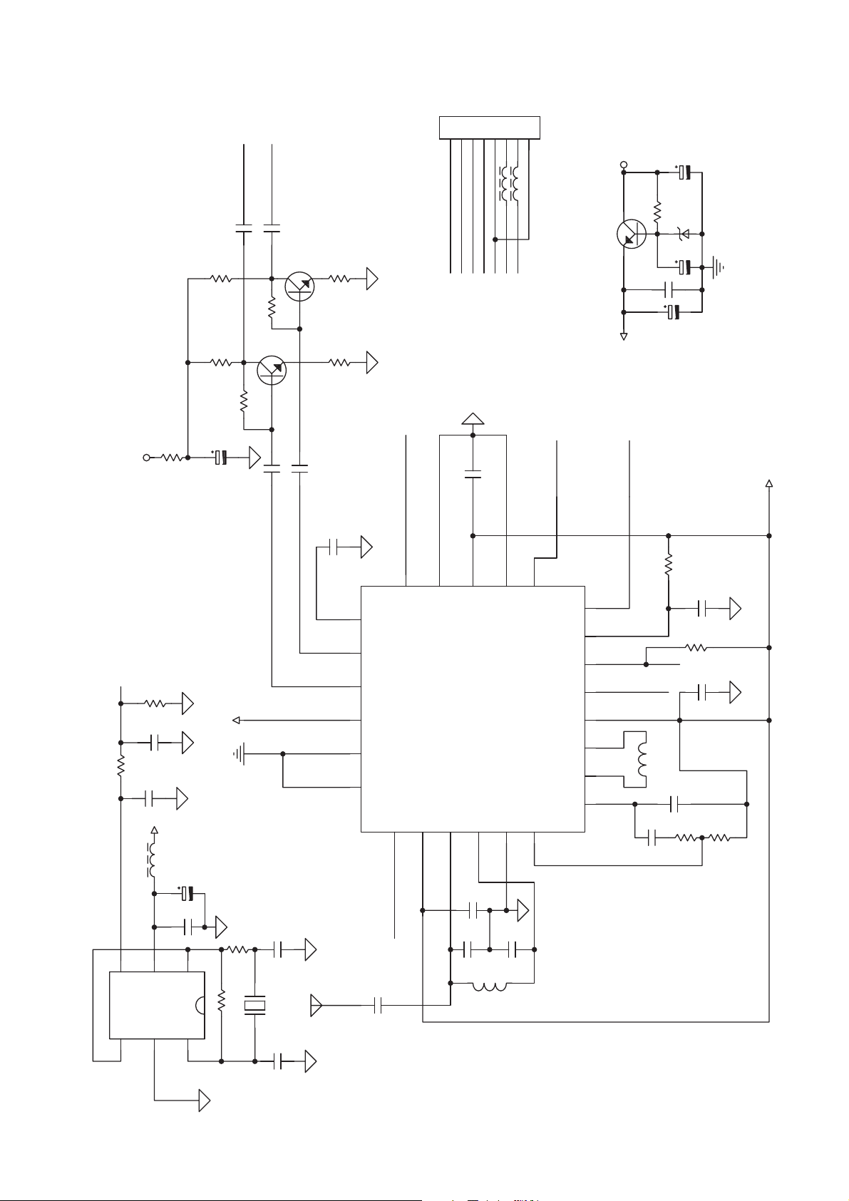
Tuner Board
circuit diagram ..........................................................................7-1
layout diagram..........................................................................7-2
VFD Board
circuit diagram ..........................................................................8-1
layout diagram..........................................................................8-2
©
Copyright 2007 Philips Consumer Electronics B.V. Eindhoven, The Netherlands
All rights reserved. No part of this publication may be reproduced, stored in a retrieval
system or transmitted, in any form or by any means, electronic, mechanical, photocopying,
or otherwise without the prior permission of Philips.
CPU Board
circuit diagram. .........................................................................9-1
layout diagram ..................................................................9-2...9-3
AMP Board
circuit diagram ........................................................................10-1
layout diagram ..............................................................10-2..10-3
MPEG Board
circuit diagram. .............................................................. 11-1..11-6
layout diagram ........................................................................11-7
Power Board
circuit diagram. .............................................................. 12-1..12-2
layout diagram ........................................................................12-3
Exploded view diagram ...............................................................13-1
Service partslist ...........................................................................14-1
Commercial partslist
Published by LX 0736 Service Audio Subject to modification
Version 1.1
3141 785 32111
Page 2

SERVICE AIDS
1-1
Service Tools:
Universal Torx driver holder .................................4822 395 91019
Torx bit T10 150mm ...........................................4822 395 50456
Torx driver set T6-T20 .........................................4822 395 50145
Torx driver T10 extended .....................................4822 395 50423
GB
All ICs and many other semi-conductors are
susceptible to electrostatic discharges (ESD).
Careless handling during repair can reduce life
drastically.
When repairing, make sure that you are
connected with the same potential as the mass
of the set via a wrist wrap with resistance.
Keep components and tools also at this
potential.
WARNING
GB
Safety regulations require that the set be restored to its original
condition and that parts which are identical with those specified,
be used
Safety components are marked by the symbol
!
.
Compact Disc:
SBC426/426A Test disc 5 + 5A ...........................4822 397 30096
SBC442 Audio Burn-in test disc 1kHz .................4822 397 30155
SBC429 Audio Signals disc .................................4822 397 30184
Dolby Pro-logic Test Disc ....................................4822 395 10216
ESD
CLASS 1
LASER PRODUCT
Lead free
Page 3
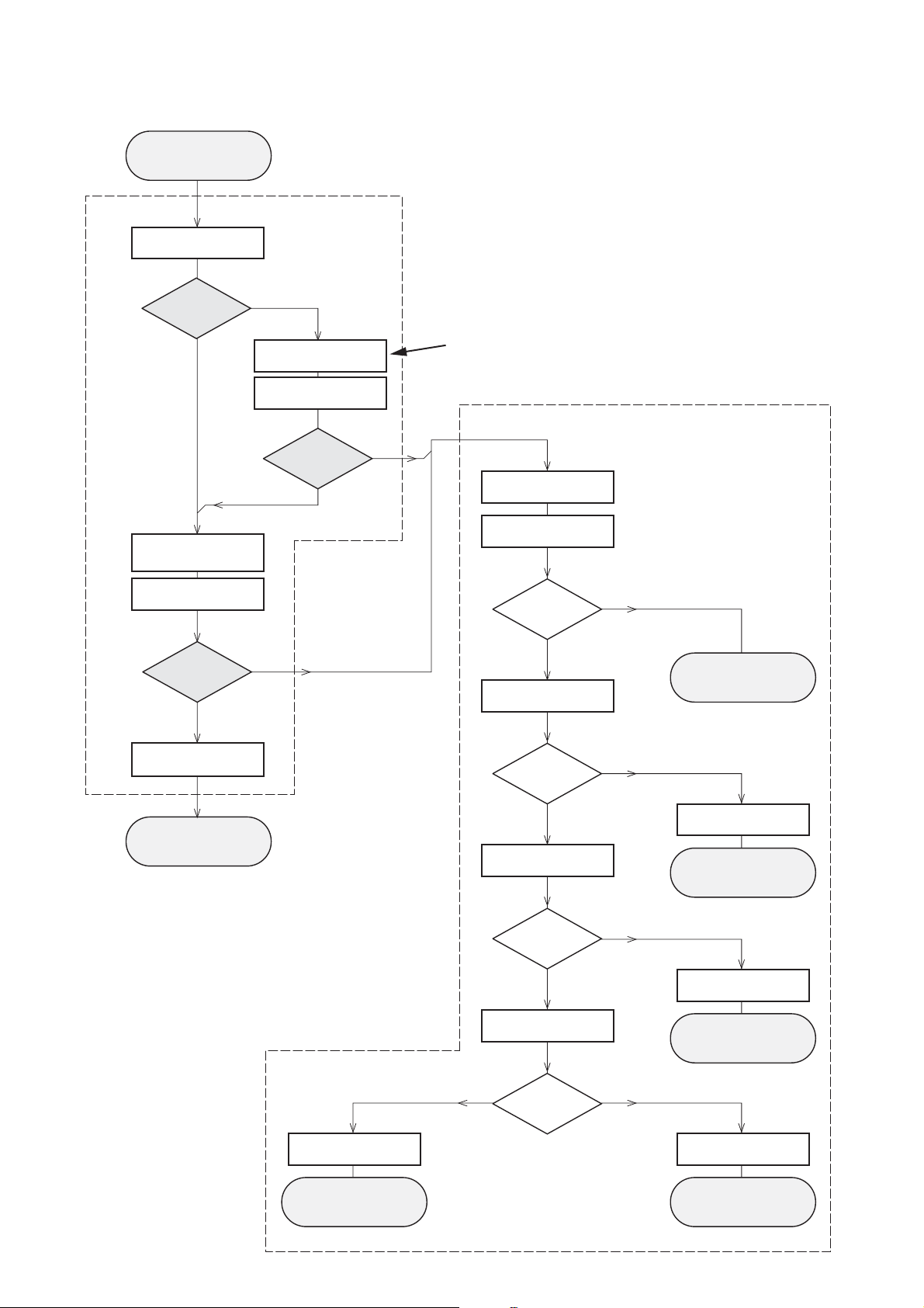
CD PLAYABILITY CHECK
Customer complaint
"CD related problem"
check playability
2 -1
Set remains closed!
1
playability
ok ?
Y
Play a CD
for at least 10 minutes
check playability
playability
ok ?
Y
add Info for customer
"SET OK"
return set
N
"fast" lens cleaning
check playability
playability
N
2
ok ?
3
For flap loaders (= access to CD drive possible)
cleaning method
4 is recommended
Standard repair procedure
N
Y
clean the lens
check playability
playability
ok ?
check "EYE-Pattern"
EYE-Pattern
ok ?
check Laser current
4
Y
N
5
N
Y
return set
replace CD Drive
6
return set
1 - 7
For description - see following pages
replace Signal Processor
return set
Laser current
ok ?
Y
check CD Drive offsets
Y
CD Drive offsets
ok ?
N
replace CD Drive
7
return set
N
replace CD Drive
return set
Page 4
CD PLAYABILITY CHECK
2-2
1
PLAYABILITY CHECK
For sets which are compatible with CD-RW discs
use CD-RW Printed Audio Disc ....................7104 099 96611
TR 3 (Fingerprint)
TR 8 (600μ Black dot) maximum at 01:00
• playback of these two tracks without audible disturbance
playing time for: Fingerprint t10seconds
Black dot from 00:50 to 01:10
• jump forward/backward (search) within a reasonable time
For all other sets
use CD-DA SBC 444A..................................4822 397 30245
TR 14 (600μ Black dot) maximum at 01:15
TR 19 (Fingerprint)
TR 10 (1000μ wedge)
• playback of all these tracks without audible disturbance
playing time for: 1000μ wedge t10seconds
Fingerprint t10seconds
Black dot from 01:05 to 01:25
• jump forward/backward (search) within a reasonable time
4
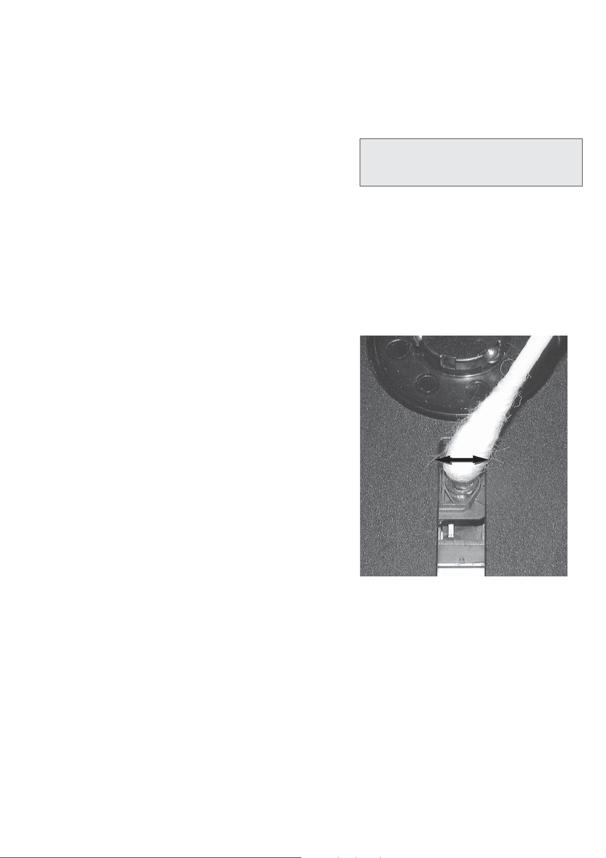
LIQUID LENS CLEANING
Before touching the lens it is advised to clean the
surface of the lens by blowing clean air over it.
This to avoid that little particles make scratches on
the lens.
Because the material of the lens is synthetic and coated
with a special anti-reflectivity layer, cleaning must be done
with a non-aggressive cleaning fluid. It is advised to use
“Cleaning Solvent B4-No2”, available with codenumber
4822 389 10026.
The actuator is a very precise mechanical component and
may not be damaged in order to guarantee its full function.
Clean the lens gently (don’t press too hard) with a soft and
clean cotton bud moistened with the special lens cleaner.
The direction of cleaning must be in the way as indicated in
the picture below.
2
CUSTOMER INFORMATION
It is proposed to add an addendum sheet to the set which
informs the customer that the set has been checked
carefully - but no fault was found.
The problem was obviously caused by a scratched, dirty or
copy-protected CD. In case problems remain, the customer
is requested to contact the workshop directly.
The lens cleaning (method 3) should be mentioned in the
addendum sheet.
The final wording in national language as well as the printing
is under responsibility of the Regional Service Organizations.
3
FAST LENS CLEANING (dry brush)
Use lens cleaning CD
SBC AC300 ...........................................9082 100 00043
Insert the lens cleaning CD, press PLAY and follow the
voice guide´s instructions on the CD.
Page 5

11
D4
CD PLAYABILITY CHECK
2-3
5
EYE-PATTERN SIGNAL – JITTER MEASUREMENT
Measure the signal on the input of the Signal processor
using an analog oscilloscope. Please find the exact
measuring point in your Service Manual.
EYE-PATTERN
800mVpp
TB = 0.5Ps/div
HF-Amplifier
+5V_HF
3920
100R
1K5
3902
220u
2885
2,4V
7876
6 (A-D)
2881
560p
3901
560R
BC847B
1,8V
2882
2883
470n
1,2V
82p
3907
820R
3908
3903
2K2
3K3
0,65V
2884
7877
BC847B
3904
470R
3906
3K3
470n
See below examples of the signal. Amplitude should read at
least 700mVpp using SBC444A.
VrefCD10
3905
2,6V
680R
2813
4n7
+3.3V
7878
BC847B
D3
D2
D1
3898
220R
3893
470R
3896
100R
47n
2818
4u7
2817
3n3
2814
3897
HFIN
28152816
LDON
to 3826,3827
3899
CD_DA: 0V / CD_RW: 3V
2K7
+3.3V
3895
2887
10
D3
9
D2
8
D1
VREF GE
7
VRIN
6
IREF
27K
5
VDDA1
47n
4
VSSA1
3
ISLICE
33K
2
HFIN
100p
1
HFREF
22n
ON
LD
64
3909
3923
10K
Sanyo
DA12T3
6
CD DRIVE – LASER CURRENT MEASUREMENT
The laser current can be measured as a voltage drop on a
resistor. The resistor is marked in every Service Manual.
The value depends on the type of CD drive.
typical value most probably defect
VAMxxxx : 150-230mV t350mV
MCDxx : 170-230mV t300mV
DA1x : 210-250mV t350mV
DA2x : 175-200mV t250mV
Use SBC444A (CD-DA) for measurement.
Laser power control
U >250mV
->Laser damaged !
+5V_HF
LASER DIODE
3817
47R
3820
4R7
470n
2876
47R
47R
3819
3818
3,9V
2V
47n
2869
3,3V
7879
BC807-40
2877
3821
47u
3822
100n
2878
1R
10K
3823
+5V
2841
100n
4,6V
7811-A
LM358D
1
3V
1K
0,17V
3
8
2880
2
4
0,17V
2879
33p
1n
good
bad
If the oscilloscope shows a signal like the ‘bad’ one, and/or
the amplitude decreases within 1 minute - the CD drive has
to be replaced.
7
CD DRIVE – OFFSET MEASUREMENT
The photodiodes of the CD-drive may have an offset. These
offsets have to be compensated by the signal processor.
High offsets can lead to poor playability of some CDs
(skipping tracks).
To measure the offset values, start the Service Test
Program - section “Focus Test” without a CD.
The offsets can be measured with a DC Millivoltmeter
directly on the connector (see drawing below). Pin
numbering varies from drive to drive.
The values from diode A-D should read 0±10mV.
Diodes E and F are less critical.
CD Drive
Sanyo DA12T3
1800
VREF
VCC
E
E
B
A
C
D
F
D
A
B
C
F
GND
If one of the offsets is higher than ±10mV the CD drive has
to be replaced. Otherwise replace the Signal Processor.
16
15
14
13
12
11
10
9
8
VrefCD10
+5V_HF
E
D
A
B
C
F
E
D
A
B
C
F
Page 6
Page:56
C
D
3 - 1
B
A1
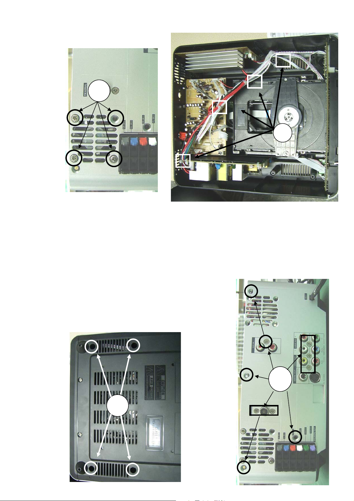
A. Remove bottom cover C. Loosen screws h15FM(4PCS),and then remove the fan
Disassembly diagram
A1. Loosen screws h3$4PCS)
B. Loosen screws h10FA(10PCS),and D.Cut off 4PCS wire tic
then remove top cover and rear shuck
Page 7

Page:57
H
I
I. Loosen screws h10BA(2PCS), remove bezel panel
F
3 - 2
G
E
E. Loosen screws h6PT(3PCS), remove CPU board HǃLoosen screws h6PT(4PCS), remove decode card
F. Loosen screws h8BA(1PC), remove AMP board
Disassembly diagram
G. Loosen screws h10PWA(4PCS), remove mechanism core
Page 8
Page:58
L
J
3 - 3
K
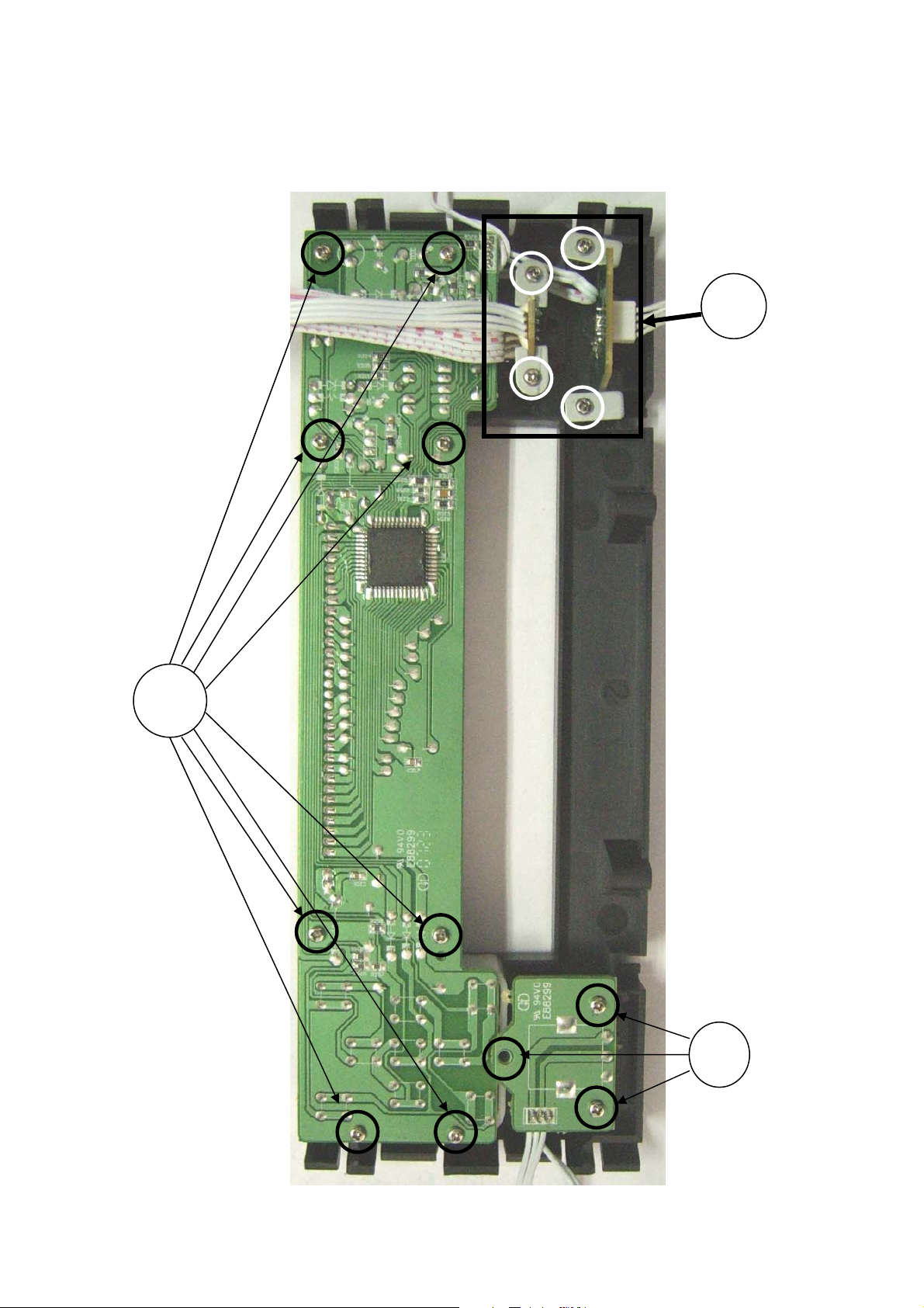
J. Loosen screws 2.h8BA(8PCS), remove VFD board
Disassembly diagram
. Loosen screws 2.h8BA(3PCS), remove volume card L. Loosen screws 2.h8BA(4PCS), remove USB, earphone socket
K
Page 9

4 - 1 4 - 1
SOFTWARE VERSION CHECK AND UPGRADING
Page 10

TDA8947J
TDA8947J
PT2322
9228
24C02
PT2323
TUNER
BLOCK
IC:TEA5760
AUX R
AUX R IN
AUX L
AUX L IN
RED
ROUT
VIDEO
V-OUT
S-VIDEO
S-V OUT
COAXIAL
OPTICAL
GREEN
GR OUT
BLUE
BOUT
MEPG2
BLOCK
MECHANISM
DVD
STBY&MUTE
CONTROL
VFD
PT16311
REM
1
GND
2
Vcc
3
REM-SENSOR
+5V
+5V
+5V
+22V
GND
DVD +12V
AC
POWER BLOCK
STANDBY
+5V
DVD ON/OFF
TUNER POWER
TUNER IN
DVD MR
DVD ML
D-FL
D-FR
SL
SR
CEN
SW
SW
CEN
SL
SR
FL
FR
FL
FR
SW
CEN
SL
SR
CPU
SDA
SCL
FR
FL
SLSRCEN
SW
KEY
CONTROL
FR
SR
CEN
SW
SL
FL
STANDBY
MUTE
SUR-MUTE
MUTE
SUR-MUTE
FM
AUX L IN
AUX R IN
TL072
+12V
-12V
+12V
-12V
SW
5 - 1
5 - 1
SET BLOCK DIAGRAM
Page 11
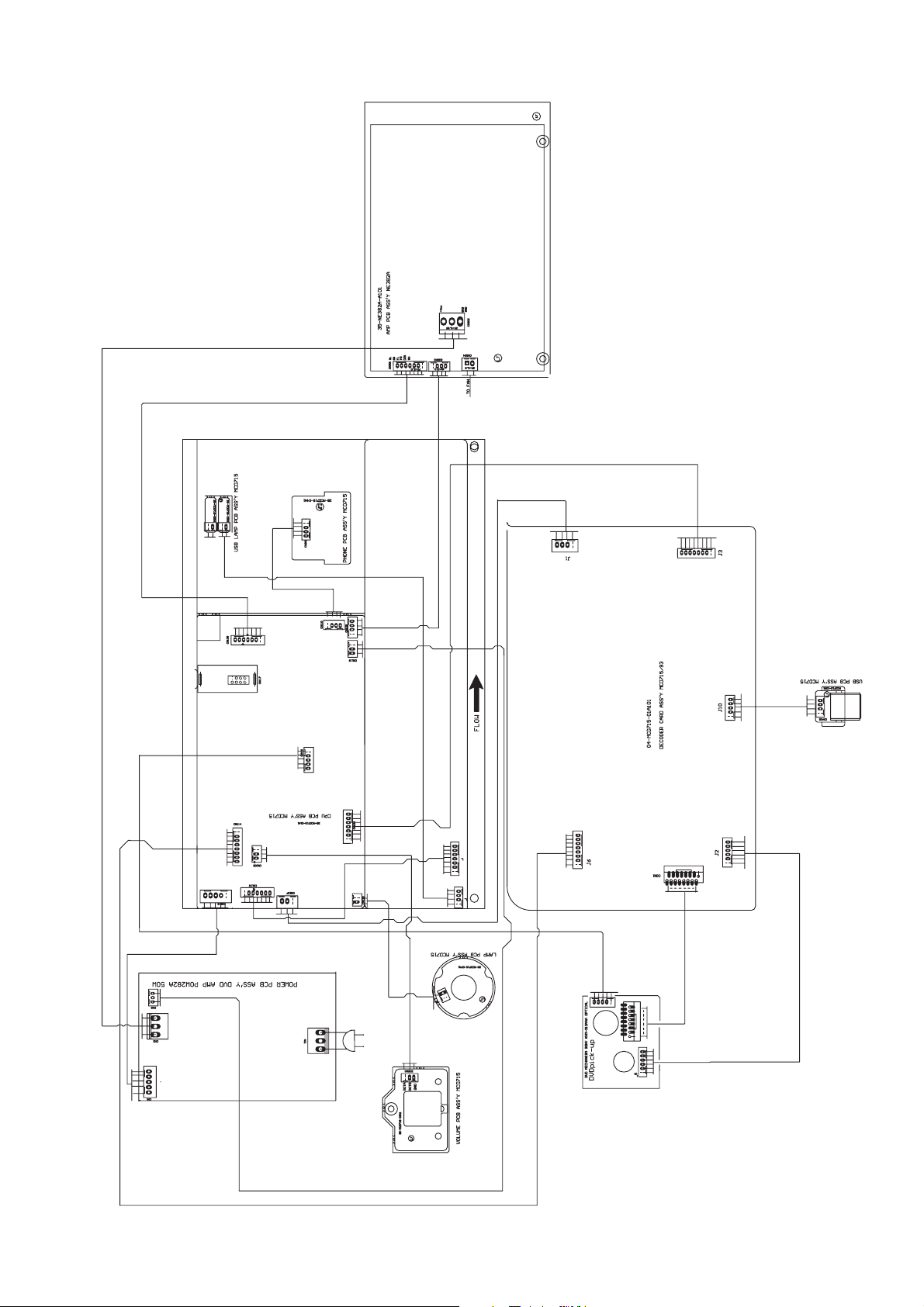
6 - 1
6 - 1
SET WIRING DIAGRAM
Page 12
7 - 1
1234567
CN1
LOUT
ROUT
224
224
C5
C4
Q3
9014
R14
224
1K
R13
1K
INTX
C12
104
R5
4.7K
R3
1M
Q2
R2
1M
C2
9014
224
C3
R4
4.7K
R1
47
+5V
C1
22uF
LOUT
ROUT
+5V
C15
SGND
SGND
103
600R
L4
SCL
600R
L5
SDA
8
8P
223
C18
330
47uF/6.3V
C19
DZ1
3.6V
C24
22uF
Q1
+5V
R22
8050
C25
47uF
3.0V
SDA
SCL
3.0V
7 - 1
CLOCK
R16
4
10K
R8
C14
C23
5
68k
10pF
100pF
3.0V
L8
10uH
C22
6
22uF
C9
104
B2
IC1
TMUTE
VAFR
VAFL
AGND
FREQIN
C1
INTX
MPXOUT
TIFcentre
VCC
A6
D6
E6
E5
MPX
E4
B5
D5
D2
DGND
C10
B6
RFIN1
D1
103
VDD
RFIN2
C6
D3
DGND
RFGND
C5
E1
DATA
LOOPSW
A2
TEA5760UK
CLOCK
VREFDIG
BUSEN
SWPORT
VccVCO
LO2
LO1
CPOUT
R19
10R
C17
103
E2
E3
C2
B1
R6
BUS_ENABLE
SW1
4.7K
C11
103
A5
A4
L7
C13
39nH
104
C16
103
R18
100K
R15
10K
A3
A1
CLOCK
C21
R12
1M
39pF
C7
27pF
C8
47pF
74HC2G04
IC2
2Y
2A
3
2
VCC
GND
1Y
R11
10M
X1
1A
1
CIRCUIT DIAGRAM - TUNER BOARD
32.768K
C20
12pF
RFIN
C6
100pF
L1
120nH
Page 13
7 - 2
7 - 2
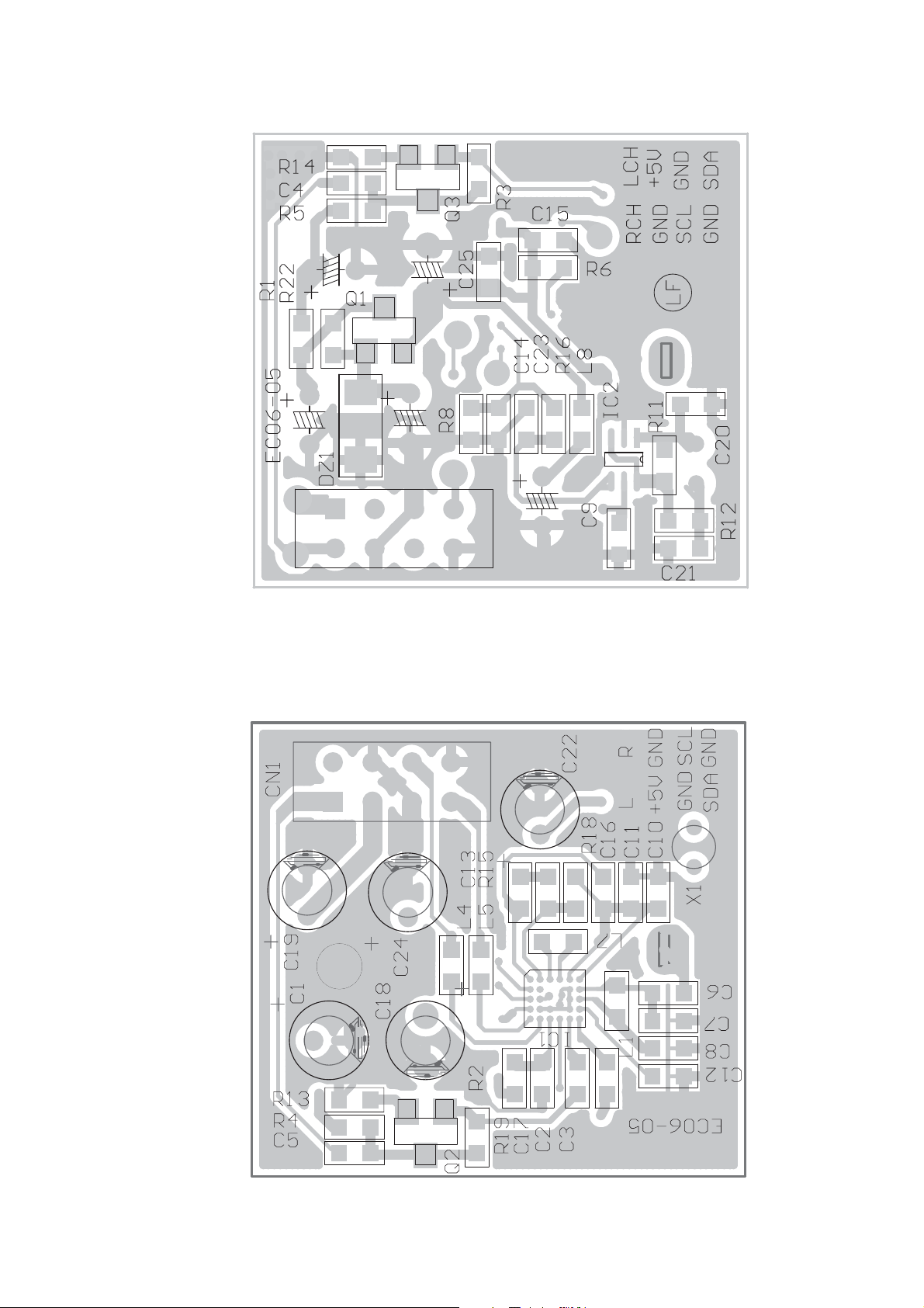
LAYOUT DIAGRAM - TUNER BOARD
Page 14

8 - 18 - 1
123
CN202
ROTA
3
MCD715-08A1
A
ENCODER
R229
0.5/0.5
C200
VFD200
NE-1300CD-3.G
123
1
2
CN501
1
2
2P/2.0
123
4
CN401
4P/2.0
VOL BLOCK
MCD715-07A1
ROTB
VGND
2
1
B
G
ENCODER800
R228
0.5/0.5W
C201
104
104
VF2
36
VF2
35
S16
34
S15
33
S14
32
S13
31
S12
30
S11
29
S10
28
S9
27
G12
26
G11
25
G10
24
G9
23
G8
22
G7
21
NC
20
NC
19
NC
18
NC
17
G6
16
G5
15
G4
14
G3
13
G2
12
G1
11
S8
10
S7
9
S6
8
S5
7
S4
6
S3
5
S2
4
S1
3
VF1
2
VF1
1
LED703
LED
R702
220
LED702
LED
R701
220
LED701
LED
R700
220
SW206
SW205
PROGRAM
SW202
SW201
OPEN
K1
K2
K1
K2
VF1-1
VF2-1
K4
-28V
3
2
1
CN001
3P
S16
S15
S14
S13
S12
S11
S10
S9
G12
G11
G10
G9
G8
G7
104P
G6
G5
C203
G4
G3
G2
G1
S8
S7
S6
S5
S4
S3
S2
S1
K3
S11
S12
26
25
S13
S13
27
S14
S14
28
S15
S12/KS12
S15
S16
G12
G11
G10
G9
G8
G7
G6
G5
G4
G3
G2
G1
S11/KS11
29
S16
30
S17/G12
31
S18/G11
32
Vdd
33
VEE
34
S19/G10
35
S20/G9
36
G8
37
G7
38
G6
39
G540G4
41
K3
KS2
4148
SW209
D207 4148
D206 4148
D205
S2
S3 KS3
S1
S10
24
19
23
20
S6/KS6
S4/KS418S5/KS5
S7/KS721S8/KS822S9/KS9
S10/KS10
IC203
uPD16311
G3
G2
Vdd45LED546LED4(BBE)47LED3(POWER)48LED2(FANCT)
G1
43
44
42
USB LED
LED3
LED4
R208
4.7K
K4
SW200
D209
17
S3/KS3
49
LED2
SW207
PLAY
SW203
PRERET+
KS2
KS3
4148
S1S2S3S4S5S6S7S8S9
15
16
S1/KS1
S2/KS2
Vss
LED1(7507RST)
51
50
47K
R254
K3
STANDBY
NES
+5V
LED
LED501
㓓㡆
PRE
PRERET-
K4K3K2
R501
SW208
SW204
K4
K1
MCD715-05A1
1K
DSC
SOURCE
KS2
KS3
R258 33K
R257 33K
R256 33K
33K
R255
14
Vdd
KEY4
13
KEY3
12
KEY2
KEY1
STB
CLK
IC
DIN
DOUT
SW4
SW3
SW2
SW1
OSC
DS-STB1
11
10
9
8
7
6
5
4
3
2
1
DS-CLK
DS-DAT
52
C217
104P
+5V
LED200
ECO-POWER
R207
0
UGND
3
5
4
2
1
MCD715-10A1
D-
D+
vbus
GND
GND
J1001
USB HOST
+5V
R232
10K
R259
4K7
R231
10K
USB BLOCK
D201
L201
+5V
ECO-power
4
CN201
RO-H
LO-H
MU-H
5
2
1
4
3
L
R
MCD715-02A1
DZ200
6.2V/1W
R210
R211
10K
R204
100
R205
VF2-1
VF1-1
6
7
B200
1
3
2
C234
473M
Q208
8050
1K
R226
C232
470/16V
4001
D204
4148
200UH
R224
X
47uF
C205
COM4
GND-H
9
678
11
10
J201
PHONE3.5
15
100
-28V
C235
220U/35V
D208
FR104
10
9
BZ1
4
5
C233
8050
Q209
R227
1K
104
R203
100
4
3
2
1
CN208
TO-USB
R206
USB LED
+5V
104
C202
0
CIRCUIT DIAGRAM - VFD BOARD
+5V
REM
DS-STB1
DS-DAT
REM
+5V
ECO-POWER
GND
DS-CLK
CN?
7P
12345
6
7
C204
GND
47
47uF
104
R260
C219
3
2
Vcc
REM1GND
S200
REMOTE
MCD715-02A1
Page 15

8 - 2 8 - 2
LAYOUT DIAGRAM - VFD BOARD
Page 16

L1
1
L2
2
L3
3
L4
4
FL-IN
5
FR-IN
6
CEN-IN
7
SW-IN
8
SL-IN
9
SR-IN
10
MIXO
11
VCC
12
REF
13
GND14SDA
15
SCL
16
SR-OUT
17
SL-OUT
18
SW-OUT
19
CEN-OUT
20
FR-OUT
21
FL-OUT
22
LPF-O
23
LPF-I
24
R4
25
R3
26
R2
27
R1
28
IC104
PT2323
R1090
270
R1089
270
R1088
270
R1087
270
R1086
270
R1085
270
C1076
683J
C1079
223J
R1055
24K
R1054
24K
C1029
4.7uF/50V
C10304.7uF/50V
C1031
4.7uF/50V
C1022
4.7uF/50V
C1021 4.7uF/50V
C1020
4.7uF/50V
C10194.7uF/50V
C10184.7uF/ 50V
C10174.7uF/ 50V
C10164.7uF/ 50V
C10154.7uF/ 50V
C10144.7uF/ 50V
C1040
10uF/25V
C1051
100uF/16V
C1053
104P
R1047
100
R1082
20K
R1081
20K
C1028
4.7uF/50V
C1027
4.7uF/50V
C1026
4.7uF/50V
C1025
4.7uF/50V
C1024
4.7uF/50V
C1023
4.7uF/50V
1
2
3
4
5
6
7
8
9
CN113
9P/2.0
D-MUTE
AGND
FLIN
FRIN
AGND
SR
SL
SW
CEN
+12V
R1063
1K
R1064
1K
D1001
4148
MUTE
AUX1-L
AUX1-R
SCL
SDA
R1061
6.8K
R1062
6.8K
R1040
100K
R1041
100K
C1089
473(M)
C1090
473(M)
C1085
10uF/16V
C1091
473(M)
C1088
473(M)
RCMID2_FR
1
RCMID1_RF2CTRE_FR3IN_FR4IN_SR5IN_SUB
6
VREF
7
GND
8
IN_CT9IN_SL10IN_FL11CTRE_FL12RCMID1_FL
13
RCMID3_FL
14
RCBAS1_FL
15
RCBAS2_FL
16
OUT_FL17OUT_SL
18
OUT_CT
19
VCC
20
OUT_SUB
21
OUT_SR22OUT_FR
23
SCL
24
SDA
25
GND
26
RCBAS2_FR27RCBAS1_FR
28
IC105
PT2322
C1102
104M
C1101
104M
C1083
103M
C1082
103M
C1080
103M
C1081
103M
R1076
3.3K
R1093
6.2K
R1092
6.2K
R1075
3.3K
R1083
20K
R1084
20K
C1086
222M
C1084
10uF/16V
C1087
222M
C1052
100uF/16V
C1056
104P
R1098
100
C1092
473(M)
C1094
104
C1093
104
SDA
SCL
FL-IN
SR-IN
+12V
C1058
4.7uF
C1057
4.7uF
CEN-IN
SW-IN
SL-IN
FR-IN
R1056 1.5K
R1057 1.5K
R1058 1.5K
R1059 1.5K
R1060 1.5K
1
3
2
J1000
RCA-2P
1
2
3
4
5
6
7
CN109
8P
TUN-L
TUN-R
IOP-L
IOP-R
AGND
123
45678
CN114
8P/2.0
+12V
REC-R
REC-L
AGND
S12V
MIC R
C1049
102
C1050
100uF/16V
R103947K
C1039
2.2uF/25V
MIC L
Q109
8050
Vcc
1
REF
2
GND
3
DGND
4
CLK
5
VCO
6
CC1
7
CC0
8
L1IN
16
L1OUT
15
L2OUT
14
L2IN
13
OUT2
12
IN2
11
IN1
10
OUT1
9
IC108
PT2399
C1012
4.7uF/50V
R1024
15K
R1014
10K
R1013
10K
R1035
22K
R1033
18K
R1010
220
R1026
15K
R1027
1K
R1034
22K
R1019
220K
C1013
4.7uF/50V
C1011
47uF/25V
R1025
15K
R1015
10K
R1016
10K
C1006
1uF/50V
D1000
4148
C1034
220uF/16V
C1010
47uF/25V
C1041
561
C1042
561
C1044
683(M)
C1045
683(M)
C1033
332
C1047
104(M)
C1046
104(M)
DZ101
5V6
MIC
R1018
6K8
R1020
5K6
+12V
R1029
1K
R1043
100
R1037
1M
R1036
47K
Q110
8050
R1046
2.2K
C1032
332
C1037
10uF/25V
C1043
103
R1021
5K6
MIC ONLY
Q108
9014
R1091
270
R1065
4.7K
R1066
4.7K
C1003
102
R1079
47K
R1008
1M
+12V
R1071
8.2K
R1017
10K
C1069
154P
R1073
3.3K
+Vs
8
OUT2
7
IN2-
6
IN2+
5
OUT1
1
IN1-
2
IN1+
3
-Vs
4
IC107
TL072
C1071
683P
C1070
334M
R1072
240K
R1070
8.2K
C1072
224P
C1055
104p
C1054
104p
R1074
3.3K
C1065
220uf
C1066
220uf
SER-IN
123
CN118
3P/2.0
R1049
100
C1064
220uF
DGND
+5V
DGND
S12V
TUN-L
TUN-R
+5V
AGND
SCL
AGND
SDA
C1075
100uF/16V
R1068
10K
R1069
10K
1
2
CN116
3P/2.5
12345
678
CN117
8P/1.0
1
2
3
4
5
CN115
5P/2.5
S12V
DGND
MUTE-O
R1053
100
R1050
100
R1051
100
C1100
330P
C1098
330P
C1097
330P
C1099
330P
123
CN107
3P/2.5
HP-MUTE
+12V
AGND
123
4
CN110
4P
R1096
150
H-OUT L
H-OUT R
R1094
1K
R1095 1K
D1003
4148
DZ102
5.1V
OUT1
1
MUTE
2
IN1
3
GND
4
IN2
5
BIAS6OUT27VDD
8
IC106
PT2309
C1096
47uF
C1095
47uF
R1097
10K
C1068
220uF
C1067
220uF
C1063 2.2uF
C1062
2.2uF
R1042
100K
D1002
4148
Q112
8050
R1067
4.7K
R1080
47K
FL-IN
FR-IN
MUTE-O
IOP-L
IOP-R
FR
FL
MIC-R
MIC-L
C1077
2.2uF
C1078
2.2uF
MUTE
1
2
3
4
CN108
4P
AGND
+12V
S-MUTE
MIC-MUTE
+12V
MIC IN
DGND
GND
C1073
10uf
X101
32.768
R1131
10K
C1109
15P
SDA
SCL
A5V
X102
4.19MHz
C1120
30P
C1121
30P
X103
32.768KHz
C1123
30P
C1124
30P
C1107
47UF/10V
C1125
104P
R1134
22K
D1006
4148
C1108
10UF/10V
SCL
SDA
MUTE
M-DOWN
36
M-UP
35
LED
34
DVD-STB
17
DVD-CLK
16
MUTE
30
PLL-DA
21
SUR-MUTE
29
RDS-SDA
19
ST/TUNED
27
SDA
26
SCL
25
TUN-ON
24
PLL-CE
23
PLL-CL
22
TEST
9
Vss
6
XT-OUT
7
XT-IN
8
M-CLOSE
32
DVD-DI
15
DVD-DO
14
DVD-ON
13
RESET
12
X-OUT
11
X-IN
10
RDS-Q
20
RDS-SCL
18
M-OPEN
33
Vdd
5
CLOSE-SW
4
DVD-TMS
3
OPEN-SW
1
ROT-A
41
KEY
2
ROT-B
42
REMTOE40DS-CLK
39
DS-DAT38DS-STB1
37
STANDBY
31
4052-A
28
M+
43
M-
44
IC101
2SC9228
STANDBY
A0
1
A1
2
A2
3
GND
4
SDA
5
SCL
6
TEST
7
Vdd
8
IC103
24C08
1
2
34567
CN104
7P/2.0
D1004
IN60
REM
R1124
68K
R1125
4.7K
DS-STB1
DS-DAT
DS-CLK
REM
ROT-A
ROT-B
R1109
10K
R1108
10K
R1110 10K
R1112 10K
C1118
103P
C1119
103P
+5V
D1005
4148
DGND
DVD IR
DVD STB
DVD CLK
DVD DATA
L101
100UH
R1128
100
DVD-ON
DVD-TMS
IPOD-TX
R1119
1K
R1120
1K
R1115
470
R1116
470
R1114
10K
R1113
10K
Q104
8050
Q103
8050
12345
CN101
5P/2.0
M-CLOSE
M-OPEN
Q102
8550
Q101
8550
OPEN-SW
CLOSE-SW
M-CLOSE
M-OPEN
OPEN-SW
CLOSE-SW
LED
M1+
M1-
DGND
+5V
C1103
220UF/16V
R1117
2.2K
R1118
2.2K
C1104
470P
C1105
470P
A5V
S-MUTE
ECO-POEWR
ROT-A
ROT-B
DGND
R1122
10K
USB-ON
+5V
Q105
8050
R1129
22K
D1007
4148
R1130
47K
C1106
220UF/16V
LED
+5V
DGND
USB-ON
DOCKCTL
IPOD-DET
1
2
3
CN105
5P/2.0
Ctrl
IPOD-TX
DOCKCTL
IPOD-DET
R1123
0
R1099
100
R1100
100
R1101
100
R1102
100
R1103
100
R1104
100
C1112
330P
C1113
330P
C1114
330P
C1115
330P
C1116
330P
C1117
330P
R1126
100
R1127
100
C1110
330P
C1111
330P
R1105
100
R1106
100
R1107
100
DVD-ON
12345
6
CN103
6P/2.0
+12V
oscI
1
oscO2Int3Vss
4
SDA
5
SCL
6
Clk
7
Vdd
8
IC102
PCF8563
A5V
123
456
7
CN119
7P/2.0
DS-STB1
DS-DAT
DS-CLK
REM
DGND
+5V
ECO-POEWR
STANDBY
DVD-ON
123
4
CN111
4P/2.0
DGND
MIC-L/R
AGND
+12V
1
2
3
4
CN102
4P/2.0
MIC-R
MIC-L
AGND
+12V
123
4
CN106
4P/2.0
R1135
47K
R1136
47K
MIC-L
MIC-R
1
2
CN120
2P/2.0
C1126
2.2UF
C1127
2.2UF
REC-R
REC-L
1
2
3
4
CN112
4P/2.0
MUTE
+12V
-12V
R1137
100 1/4W
V21SNAF
9 - 1
9 - 1
CIRCUIT DIAGARM - CPU BOARD
Page 17

9 - 2
9 - 2
LAYOUT DIAGARM - CPU BOARD
Page 18

9 - 3
9 - 3
LAYOUT DIAGRAM - CPU BOARD
Page 19

10 - 1
000
000
R342
R341
CENOUT-
Vcc
CENOUT+
C310
LOUT-
ROUT+
SWOUT-
Vcc
C325
1000uF/25V
C308
104
R327
10K
12V
DZ300
15K
Q301
8050
R325
1.5K
IC300
R323
8050
Q300
R321
270
C322
ROUT
1
IN1+8IN3+
223
223
C318
R309
2.2K
R317
FRIN
OUT1+
2.2K
6
C319
47K
R316
FLIN
1000uF
LOUT
4
OUT2-
IN2+
C312
C311
9
C320
1000uF
C321
14
1uF
102
OUT3-
IN4+12CIV
102
1K
R318
SWIN
C309
104
17
16
3
OUT3+
13
C316
22u/25V
R310
R308
2
GND215VCC2
11
47K
333
C328
SVR
D301
7
4148
R331
GND1
TDA8947J
MODE2
SGND
MODE1
5
10
C332
2.2uF
C329
100u/25V
4.7K
R332
4.7K
Q304
8050
R311
47K
R319
1K
R330
4.7K
C326
10uF/16
VCC1
47K
15K
R324
Q302
R322
R328
8050
10K
12V
DZ301
R326
1.5K
Q303
8050
270
SWOUT+
SLO-
SRO+
1
IN1+
IC301
8
474
C333
R315
R314
4.7K
R335
SRIN
OUT1+
47K
474
C334
4.7K
R334
17
3
15
2
OUT3-
102
10K
R329
CENIN
OUT3+
IN4+12CIV
16
VCC1
GND2
GND1
VCC2
SVR
SGND
MODE1
7
11
C317
10
22u/25V
D304
4148
R338
000
4.7K
R336
102
47K
Q305
8050
C313
R320
1K
13
R313
4
14
OUT2-
IN2+
IN3+
6
9
C335
474
C315
47K
C314
102
SLIN
D302
D300
4148
MUTE
5
R333
MUTE
AGND AGND
104
000
000
L300
2
1
2P/2.5
C336
47/16V
ONLY FAN
+12V
R343
0.47/0.25
J300 000
CN304
FAN
R340
R339
TDA8947J
MODE2
C331
100u/25V
C330
100u/25V
4.7K
R337
R312
47K
4.7K
C327
10uF/16
D303
4148
4148
SUR-MUTE
10 - 1
CIRCUIT DIAGRAM - AMP BOARD
CENOUT+
CENOUT-
SLO-
SRO+
SWOUT+
SWOUT-
LOUT
ROUT
R305
R304
R303
R301
R300
R306
R307
2.2R
R302
2.2R
2.2R
2.2R
2.2R
2.2R
2.2R
C307
104
2.2
C306
104
C305
C304
C303
C302
C301
C300
104
104
104
104
7P/2.0
CN301
104
104
CN300
WP12-2
56789
432
1
SWOUT-
SWOUT+
CENOUT+
10
11
12
PGND
PGND
LOUT-
ROUT+
PGND
CENOUT-
PGND
CENIN
SLIN
SWIN
FLIN
FRIN
AGND
SRIN
234
567
Vcc
PGND
2
3
1
CN302
MUTE
SUR-MUTE
+12V
DGND
1
3P/3.95
123
4
CN303
4P/2.0
SROUT+
SLOUT-
SRO+
1000uF
C324
SLO-
C323
1000uF
Page 20

10 - 2
10 - 2
LAYOUT DIAGRAM - AMP BOARD
Page 21

10 - 310 - 3
LAYOUT DIAGRAM - AMP BOARD
Page 22

Standby 5
URST# 2
Y5
Y4
Y2
Y1
VCC
+12V
L3
U1 MP9141
100uH_1.7A
C1 0.01uF
45
123
BS
VIN
VSW
COMP
EN
SYNC
678
GNDFB
+
D1
SK34/SMD
CB2
R5
CB1
0.1uF
CE2
220uF/16V
0.1uF
10K
Standby
URST#
1 2
CB4
R8
750/NC
0.1uF
R9
390/NC
V18
L4 FB/NC
CB69
CB68
CB67
CB66
R2
3.3K
R1
27K
VCC
R3 150K
11 - 1 11 - 1
+12V
VCC
L2
L1
FB/DIP/3.5*4.7
P5V
P+12V
Standby
123
4
CIRCUIT DIAGRAM - MPEG BOARD
PART 1
J1
C2
0.022uF
C3
100pF
R4
300K
Standby
CE1
220uF/16V
+
FB/DIP/3.5*4.7/NC
CON2.54-4
R6
15K
89L_3V3
L5
V33
2
OUTIN
GND
1
U2 1117-ADJ/NC
3
+2.5v
CB5
0.1uF
RFV33
CE6
47uF/16v
+
CB3
0.1uF
CE3
220uF/16v
+
FB
DV33
L7 FB
CB6
0.1uF
RESET Circuit
+
L6
FB
CE5
220uF/16v
DV33
R170
URST#
CB70
0.1uF
R171 1K
CB70 must closer to PIN43 of
1389L
10k
Q27
3904
1 3
2
R172
1k
R173
10k
+
CE49
10uF/16v
D13
1 2
1N4148
Page 23

11 - 211 - 2
89L_3V3
V18
DQ[0..15]
APLLVDD3
47uH/0805
L9
L8 47uH/0805
ADACVDD
RFVDD3
L11
89L_3V3
89L_3V3
CB7 0.1uF
RFV18-1
V18
DQ[0..15] 4
MA[0..11] 4
DQM[0..1] 4
BA[0..1] 4
RAS# 4
CAS# 4
WE# 4
SF_DI 4
SF_CK 4
SF_CS 4
L12 FB
3DDVCAD 3DDVCAD
L10 FB
MA[0..11]
CE7
+
CB12
CB11
CB10
CB9
C5
FB
CB8 0.1uF
RFV18-2V18
L13 FB
DQM[0..1]
thrice resonance
10uF/16V
0.1uF
0.1uF
0.1uF
0.1uF
4.7uF
BA[0..1]
R10 100K
crystal need add
DCLK 4
CAS#
RAS#
DCLK
XOXI
Y3
L14 2.7uH/NC
SERVO RF DeCAP.
J2
6
SP-A
DV33
WE#
CKE
C8
27MHz
C7
C6
1000pF/NC
5
LIMIT
R11 10K
SP+
CKE 4
DRAM I/F
22pF
22pF
RFV33
4
SL-
L15
V1P4
V20
123
SL+
SF_CK
AADVDD
+
CB14
+
CB13
SF_CS
SF_DI
CE10
+
C9
47uH/0805
CE9
47uF/16V
0.1uF
CE8
47uF/16V
0.1uF
CON2.0-6
SF_DO 4
SF_DO
S-FLASH
+
CE12220uF/16V
220uF/16V
6800pF
OP-
R12 10K
SP-
ALF 5
ALF
CE11 100uF/16V
+
CB15 0.1uF
RF Reference
DV33
1
CB17 0.1uF
ALS
R13
ALS 5
CB16 0.1uF
ARS 5
ARS
2
D3
ARF 5
AR 5
ARF
ALARASPDIF
C11 10uF/10V
C10 4.7uF
RFO
C12 10uF/10V
ADVCM
BAT54C
3
CB18
0.1uF
1/0805
R14 NC
SP+
AL 5
ASPDIF 6
C13 1500pF
C15
C14
1uF
CB19 0.1uF
OPO
R16 10K
R15 0
SP-A
220pF
MDI2
R17 0
MDI1
R18
V_G/Y
V_B/U
V_R/V
OP-
FS
AR
AVCM
AL
2K
ALS
ALF
V_CVBS 6
V_R/V
V_CVBS
AUDIO I/F
89L_3V3
V_CVBS
DACVDD3
DACVDD3
OUT3
ADVCM
IO_USB
AADVDD
APLLVDD3
ARF
ARS
ADACVDD
RFV18-1
1389_OP+
1389_OP+OPO
FGOPO
R19 0
R20 0/NC
V_B/U 6
V_G/Y 6
V_R/V 6
V_B/U
V_G/Y
97
98
99
100
101
G
102
B
103
R
104
105
106
107
108
109
110
111
112
113
114
115
116
117
118
119
120
121
122
123
124
125
126
127
128
129
U3
+5VS
STBY 3
STBY
VIDEO I/F
CB20 0.1uF
VREF1
96
FS
DACVSSC
CVBS
DACVDDB
DACVDDA
AADVSS
AADVDD
APLLVDD
APLLCAP
ADACVSS2
ADACVSS1
ARF / GPIO
ARS / GPIO
AR / GPIO0
AVCM
AL / GPIO1
ALS / GPIO
ALF / GPIO
ADACVDD1
ADACVDD2
AVDD18
AGND18
RFIP
PAD_GND
1
R23 0
R22 10K
Q1
R21 4.7K
TRIN 3
TROUT 3
TRIN
TROUT
ASPDIF
DACVDD3
TRIN
949093
95
VREF
GPIO13
DACVDDC
ADVCM / GPIO20
RFIN / OPOUT
RFG / OPINP
RFH / OPINN
RFC
RFB
RFA
4
3
2
R25 0
R26 0
R27 0
BECDF
A
IOA
R24 10K
2
2N3904
T- 3
T+ 3
F- 3
F-T-F+
T+
V18
GPIO11
TRCLOSE
TxD
RxD
92
91
898884
GPIO9
GPIO11
GPIO10
DVDD18
SPDIF / GPIO12
AKIN2 / GPIO19 / Audio_Mute
AKIN1 / GPIO21 / Audio_Mute
RFD
RFE
RFF
AVDD18
AVDD33
5
789
6
R29 0
R28 0
XI
RFVDD3
RFV18-2
1 3
F+ 3
SL- 3
SL+ 3
SP- 3
SP+ 3
FOSO 3
TRSO 3
FMSO 3
DMSO 3
SL+
SL-
SP-
SP+
TRSO
FOSO
FMSO
DMSO
MA1
MA2
BA1
MA10
CKE
MA0
MA3
81
87
80
86
82
BA1
RA3
RA2
RA1
RA0
RA10
GPIO8
DVDD33V14
GPIO7 / CKE
LQFP 128
MT1389L/K
XTALI
XTALO
AGND
V20
REXT
MDI1
MDI2
LDO1
101112
16171819202122
13
15
14
MDI2
MDI1
V20
V1P4
R34 0
LDO1
R31 15K
XO
89L_3V3
VCC
L17
FB
CE13
+
+5VS
L16
FB
CB21
R30 4.7K
2
Q3
2N3904
R33
1 3
1 3
R32
2
Q2
2N3904
SONY313
798583
DVSS18
Desktop
LDO2
R35 0
LDO2
V1P4
BA0
78
AVDD33
L18 FB
100uF/16V
0.1uF
100
100
V1P4 3
SERVO I/F
CAS#
RAS#
WE#
77
76
75
BA0
RAS#
CAS#
RWE#
V1.0
AVDD33
DMO
FMO
TRAY_OPEN
DMO
STBY
FMO
CB22
0.1uF
C16
4.7uF
CON1
USB_DP 6
USB_DP
USB_DM
MA4
MA6
MA7
MA8
MA9
MA5
72
68
73
74
71
RA9
RA8
RA4
RA5
RA6
RA7
TRAY_CLOSE
TRO
FOO
FG / GPIO2
USB_DP
USB_DM
25
26272829303132
23
24
USB_DM
IOA
TRO
USB_DP
USB_V33
FOO
FG
C19
10uF/10V
0.1uF
CB23
89L_3V3
Very Important to
reduce Noise
C18 NC
C17 NC
LD-DVD
MDI1
AVCC1
22
26
21
25
23
24
URST# 1
USB_DM 6
URST#
USB I/F
DCLK
MA11
DQM1
65
66
676970
RA11
RCLK
DQM1
DVDD33
USB_V33
USB_GND
PAD_VRT
USB_V18
USB_V18
CB24
0.1uF
C20 NC
R36 5.1K
C21
10uF/10V
L19 FB
L20 FB
V18
CB25 0.1uF
LD-CDEV20FA
AVCC1
16
17
13
14
181920
15
URST
MT1389L
LQFP128/SMD/1389L
RD8
64
RD9
63
RD10
62
RD11
61
DVSS33
60
RD12
59
RD13
58
RD14
57
RD15
56
DQM0
55
DVDD18
54
RD7
53
RD6
52
RD5
51
DVDD33
50
RD4
49
RD3
48
RD2
47
RD1
46
RD0
45
IR
44
PRST#
43
ICE
42
UP1_7 / SDA
41
UP1_6 / SCL
40
SF_CK
39
SF_DI
38
SF_DO
37
SF_CS_
36
GPIO6
35
GPIO4
34
GPIO3 / INT#
33
LDO2
R37
L22
10uH/SMD
L21
10uH/SMD
B
9
12
10
11
TOP
TRCLOSE 3
TROPEN 3
OUT1 4
OUT2 4
TRCLOSE
TROPEN
OUT1
OUT2
CE14
100uF/16V
+
Q5
0
Q4
2
8550/DIP
C22
NC
IOA
C
RFODF+
T-
5
6
7
4
8
2N3906
CE15
T+
3
R38 10K
2
+
1 3
2
DQ8
DQ9
DQ10
DQ11
DQ12
DQ13
DQ14
DQ15
DQM0
DQ7
DQ6
DQ5
89L_3V3 V18
DQ4
DQ3
DQ2
DQ1
DQ0
IR
URST#
ICE
UP1_7
UP1_6
SF_CK
SF_DI
SF_DO
SF_CS
TROPEN
LIMIT
TROUT
RFV33
1 3
47uF/16V
R39 4.7
R40 4.7
F-
1
HEADER 24 SMD0.5 TOP
TP1
13
R41 10K
Q6
2
CE16
+
CE17
+
2N3906
47uF/16V
2
13
DV33
100uF/16V
R42
Q7
8550/DIP
0
J3
OUT3
R47 1K
R46 1K
R45 1K
R44 1K
LDO1
FOO
R43 27K
FOSO
9
TRO
R48 27K
TRSO
OUT2
FMO
R49 15K
FMSO
OUT1
DMO
R50 10K
DMSO
678
IO_USB
VSDA
R51 0
UP1_7
C25
CB26
C24
C23
CON2.0-9
1
5
234
VSTB
VSCK
REM
C32
100pF
C31
100pF
C30
100pF
IR/VFD
R52 0
R53 0
R54 10
C29
100pF
C28
100pF/NC
C27
100pF/NC
C26
100pF/NC
GPIO11
IR
UP1_6
J4
CON2.0-4
123
4
RxD
TxD
DV33
RS-232
CB32
0.1uF
CB31
V1889L_3V3
0.1uF
CB30
0.1uF
CB29
0.1uF
Chip Decap.
CB28
0.1uF
CB27
0.1uF
V1P4
0.015uF
0.1uF
330pF
330pF
CIRCUIT DIAGRAM - MPEG BOARD
PART 2
Page 24

TRIN 2
STBY 2
TROPEN 2
TRCLOSE 2
T+ 2
SL- 2
T- 2
SL+ 2
F+ 2
F- 2
SP- 2
TROUT 2
SP+ 2
V1P4 2
DMSO 2
FMSO 2
FOSO 2
TRSO 2
TROPENF-TROUT
STBY
TRIN
TRCLOSE
+2.5V
T+
F+
D5
D4
SL-
SL+
VCC
12
1
2
MO_VCC
SP+
SP-
FOSO
IN4001/DIP
IN4001/DIP
D6
12
TRSO
DMSO
IN4001/DIP
V1P4T-FMSO
V18
Q8
23
1
DMSO
SERVO I/F
CB35
+
8550/DIP
R58
4.7K
R60
IN4001/DIP
VCC
0.1uF
CE19
100uF/16V
10K
D7
12
8550/DIP
23
1
TR_B2
L23
V33
Q9
V18=(R58/R60+1)*1.25
FB
CB37
MO_VCC
R62
+
CE20
15K
0.1uF
100uF/16V
CE21
+
CB39
CB38
REGO2
100uF/16V
0.1uF
0.1uF
R64
9.1K
11 - 3 11 - 3
CIRCUIT DIAGRAM - MPEG BOARD
PART 3
L24 FB
FOSOSTBY
29
30
G1G2
TROPEN
6
7
5
REV
FWD
VINLD
GND
24
22
23
FMSO
R57 10K
REGO2
4
3
VINSL+
REGO1
TRB2
NC
25
26
TRSO
TR_B2
1
2
TRB1
REGO2
VINTK
BIAS
27
28
V1P4
CB33
VINFC
MUTE
AM5888
HSOP28/SMD
CB34
R59
0.1uF
0.1uF
10K
DV33
VCC
J5
1
LOAD-
LOAD+
CB36 0.1uF
234
TROUT
R61 10K
5
TRIN
R63 10K
CON2.0-5
+F-T
SP-
LOAD+
SP+
LOAD-F-TRCLOSE
91012
14
13
11
8
VCC
VOSL-
VOFC-
VOTR-
VOSL+
VOFC+
VOTR+
VOLD+
VOLD-
VOTK-
VOTK+
U4
15
VCTL
VCC2
NC
17
21
19
20
18
16
T+
SL+
SL-
R55 10K
R56 10K
MO_VCC
Page 25

DQ[0..15] 2
MA[0..11] 2
DQM[0..1] 2
BA[0..1] 2
DCLK 2
RAS# 2
CAS# 2
WE# 2
CKE 2
SF_CK 2
SF_DI 2
SF_CS 2
SF_DO 2
CVBS_EN 6
16:9B 6
16:9A 6
RGB_SWITCH 6
OUT2 2
AUDIO_MUTE 5
OUT1 2
11 - 411 - 4
DQ[0..15]
MA[0..11]
DQM[0..1]
DQ1
DQ0
DQ2
BA[0..1]
DQ4
DQ3
DCLK
SD33DV33
DQ5
RAS#
DQ6
CAS#
SD33
L25 FB
DQ7
WE#
DQ8
CKE
DQ9
CB42
CB41
CB40
CE23
+
CE22
+
DQ10
DRAM I/F
0.1uF
0.1uF
0.1uF
100uF/16V
47uF/16V
DQ12
DQ13
DQ11
DQ14
SF_CK
SF_CS
DQ15
SF_DI
SF_DO
SD33
S-FLASH
SD33
SD33
CVBS_EN
CB47
0.1uF
CB46
0.1uF
CB45
0.1uF
CB44
0.1uF
CB43
0.1uF
I/O
16:9A
16:9B
RGB_SWITCH
SCART
DV33
AUDIO_MUTE
OUT1
OUT2
OUT1
16:9A
CVBS_EN
16:9B
RGB_SWITCH
2
569121516192010
Q0Q1Q2Q3Q4Q5Q6
VCC
D0D1D2D3D4D5D6D7OC
U6
347
8
131417
MA4
MA0
MA3
MA5
MA6
MA1
MA2
DV33
NOR
2TUO7AM
AUDIO_MUTE
Q7
1
18
5
VCC
U8
ABGND Y
213
GND
G
74LCX373
11
4
SN74AHC1G02
2
4
DQ0
A0A1A2
U5
23
242526
MA0
MA1
SDRAM
CIRCUIT DIAGRAM - MPEG BOARD
PART 4
DQ1
MA2
5
798
DQ2
MA3
104611
DQ3
DQ4
DQ5
A3
A4A5A6A7A8
29
3031323334
MA4
MA6
MA5
DCS#
R65 10K
DQ6
MA7
50
51
DQ13
BA1/A12
21
DBA1
53
DQ14
DQ15
CLK
38
SDCLK
CKE
37
SDCKE
SDCLK
DBA0
R67 0
R66 33
BA0
DCLK
1
VCC
CS
19
DCS#
DBA1
R68 0
BA1
14
VCC
RAS
DCAS#
DRAS#
VCC
CAS
161718
DWE#
RN1 0x4
3627
VCCQ
WE
DRAS#
234
1
RAS#
43
VCCQ
DQML
39
15
DQM0
DQM1
DWE#
DCAS#
5 6
WE#
CAS#
49
VCCQ
VCCQ
DQMH
SDCKE
7 8
CKE
12
52
VSSQ
VSSQ
VSSQ
VSSQ
VSS
NC
NC
VSS
VSS
ESMT M12L64164A
41
40
36
54
28
R169 10K
DV33
DRAM EXTENSION GPO
DV33
R69 10K
DV33
SF_CK
8
7
6
VDD
HOLD#
CE#SOWP#
U7
123
SF_DO
SF_CS
R70 10K
S-FLASH
DV33
CB48
SF_DI
SCK
4 5
VSS SI
DRAS#
SDCKE
0.1uF
EN25B80
8M bit
DV33
R72 10K/NC
SF_CS
R71 10K
45
48
13
42
44
47
DQ8
DQ9
DQ7
DQ10
DQ11
DQ12
A11
A10/AP
A9
BA0/A13
22
20
35
DBA0
MA11
MA8
MA10
MA9
Page 26

AL 2
AR 2
ALS 2
ALF 2
ALARALS
ARS
ALFMLMRFLFR
ARS 2
ARF 2
ML 6
MR 6
FL 6
FR 6
Standby 1
AUDIO_MUTE 4
ARF
Standby
AUDIO_MUTE
AUDIO I/F
11 - 5 11 - 5
R74
ML
L26 FB
10K
+
CE24 10uF/16V
C33 120pF
C34
R76
Q10
2
A_MUTE
100pF
47K
2N3904
A_MUTE
Q14
2N3906
1 3
CE27
100uF/16V
+
D10
Q11
2N3904
1 3
2
R91
10K
1N4148/SMD
D9
R82
1M
CE28
10uF/16V
1K/0805
Q12
2N3906
1 3
2
R87
43K
1 2
MR
L27 FB
C37
100pF
47K
R86
Q13
2N3904
2
R89
R85 10K
A_MUTE
+
C36 120pF
R83
D8
1N4148/SMD
1 2
+12V_OUT
FL
1 3
R80
100
1K
R77
+
CE26
10uF/16V
1
U9A
C4558
+
-
8 4
3
2
2
R90
10K
1N4148/SMD
DV33
CE29
+
1 3
1K
R94
CE31
1 2
R95
10uF/16V
FR
100
+
10uF/16V
7
-
6
R96
D11
+
5
10K
R97
33
10K
4.3V/SMD
U9B
C4558
8 4
AUDIO_MUTE
MUTE_Circuit
CB50
0.1uF
+12A
CB49
0.1uF
VREF
NC
C39 120pF
R102
CE33
SL
100
+
10uF/16V
1
-
2
J6
1
2
345
+12V_OUT
R105
100
CE35
+
+12A
R104
10K
+
VREF
CE34
U10A
C4558
+
8 4
3
100uF/16V
R106
10K
220uF/16V
SUBFRSLFLCENSRA_MUTE
678
C41 120pF
CON2.0-8
R110
100
CE37
10uF/16V
-
Standby
R115
20K
R116
Q16
C43 120pF
2N3904
10K
R119
100
CE39
10uF/16V
-
SUB
+
1
U11A
C4558
+
8 4
3
2
C45 120pF
R124
CE41
CEN
100
+
10uF/16V
7
-
6
CB54
0.1uF
U11B
C4558
+12A
+
8 4
5
VREF
CB53
0.1uF
+12V
+12V_OUT
SR
+
7
U10B
C4558
+
8 4
5
6
R113
100K
Q15
AO3407
+12A
VREF
CB52
CB51
0.1uF
0.1uF
10K
R112
R79
5.1K
C35
CE25
2200pF
R78
10K
+
10uF/16V
R81
100K
AL
R73 33K
R75
0/NC
CIRCUIT DIAGRAM - MPEG BOARD
PART 5
R93
5.1K
R84 33K
R92
R88
0/NC
+
CE30
AR
10K
C38
10uF/16V
2200pF
R101
5.1K
R99 33K
R98
100K
CE32
R100
+
10uF/16V
C40
2200pF
10K
R103
100K
ALS
R109
5.1K
C42
CE36
2200pF
R108
10K
+
10uF/16V
R111
100K
ARS
R107 33K
R118
5.1K
C44
CE38
R117
+
10uF/16V
2200pF
10K
R120
100k
ARF
R114 33K
R123
5.1K
C46
CE40
2200pF
R122
10K
+
10uF/16V
R125
100K
ALF
R121 33K
Page 27

SC
SY
11 - 611 - 6
CVBS_EN
+5VV
7
4
ML 5
FR 5
MR 5
ASPDIF 2
FL 5
USB_DP 2
V_G/Y 2
V_CVBS 2
V_R/V 2
CVBS_EN 4
V_CVBS
V_B/U
V_R/V
16:9
R127
+12V
+5VV
L28 FB
VCC
CB55
0.1uF
R126
3.3K
V_B/U 2
V_G/Y
R128
680
DV33
CB56
0.1uF
Q17
CE42
L29
VIDEO I/F
R129
75
4.7K
R133
DV33
1K
R131
4.7K
CE43
220uF/16V
+
G/Y
2N3904
1 3
2
R132
+
C48
22uF/16V
C47
1.8uH/SMD
USB_DP
2.2K
R134
2.2K
USB_DM 2
USB_DM
Q19
2
R136
16:9B
Q18
2
R135
16:9A
75 1%
47pF
47pF
2N3904
2N3904
RGB_SWITCH 4
16:9B 4
16:9A 4
P1
J7
R147
CON2.0-3
4.7K/NC
123
CVBS_IN
CTR_IPOD
CE45
U12
C51
220uF/16v
NJM2244
10uF/0805
R148 0
CVBS
+
7
OUT
IN-1
1
CVBS_IN
+5VV
DASW-10
2
SW1
IN-2
3
R1490
CVBS1
4
5
C52
SW2
IN-3
FB
10uF/0805
R151
CB60
R150
6 8
L31
R152
8
9
G/YMLB/U
MR
C54
47pF
100/NC
R155
C53
0.1uF
VCC GND
C55
4.7uF/16V/0805
R154
100/NC
R153
100/NC
75/NC
75/NC
0.1uF
3.3K
CE46
L32
Q23
2
2N3904
+
6
R/V
1 3
R157
C57
22uF/16V
C56
1.8uH/SMD
5
+5VV
R158
75 1%
2.2K
47pF
47pF
MR
ML
ASPDIFFLFR
USB
1 3
1 3
DV33
2.2K
+5VV
AUDIO I/F
RGB/CVBS#
Q20
2N3906
1 3
R137 33
16:9B
16:9A
RGB_SWITCH
SCART
CVBS_EN
0/NC
R146
CB58
0.1uF
2
VCC
R140
2.2K
4.7K
R139
RGB_SWITCH
B/U
CB57
0.1uF
+5VV
Q21
2N3904
1 3
R143
75 1%
2
R138
R142
2.2K
3.3K
+
C50
47pF
CE44
22uF/16V
L30
1.8uH/SMD
C49
47pF
R144 0/NC
CVBS1 CVBS
+12V
SC
CB59
0.1uF
Q22
2N3904
1 3
R145
75 1%
2
1013111214
1
3
CVBS
CB61
0.1uF
GG
CY
2
15
16
COXIAL
R/V
COXIAL
C58
0.1uF
C59
330pF
R161
100
R159
100
SY
Q24
2N3904
1 3
R160
75 1%
2
J8
CON2.0-3
+5VV
123
SPDIF
R162 33
ASPDIF
VCC
C60
J9
123456789
CB63
0.1uF
CE47
47uF/16v
+
R163
22
27pF/NC
0.1uF
CB62
R164
3.3K
CE48
1.8uH/SMD
L33
CVBS_ST
Q25
2
+
R/V
2N3904
G/YFLFR
CVBS_ST
1 3
22uF/16V
B/U
2
R166
C62
C61
10
RGB/CVBS#
16:9
D12
DIODE SMD BAV99
R167
75 1%
2.2K
47pF
47pF
CON2.0-10
+5VV
3
1
J10
CON2.0-4
3
4
2
1
CB65
0.1uF
USB_DP
PWR2
PWR2
USB_DM
F1
500mA/NC
L34 FB/1206
VCC
Only for MT1389L
CVBS1
CB64
0.1uF
Q26
2N3904
+5VV
1 3
R168
75 1%
2
R130
V_G/Y
160 1%
CIRCUIT DIAGRAM - MPEG BOARD
PART 6
V_B/U
R165
V_CVBS
R141
160 1%
V_R/V
R156
160 1%
160 1%
Page 28

11 - 7 11 - 7
LAYOUT DIAGRAM - MPEG BOARD
Page 29

12-1
R97 4.7R 1W
+1 2 V
S
F2
ZD2
R41
6.2V 1/2W
100R 1206
6
-24 V
D9
8
F1
R42 10K 1206
R47
100R 1206
7
FR104
CE15
CE11
CE7
47uF/50V
47uF/50V
47uF/50V
GND
+1 2V
4800U5
L3 DR6*8
D12
UF5404
11
12
0R 1206
R55
CE10
1000uF/16V
CE6
1000uF/16V
+5 V
10uH
R48
D10
1N5819
9
R61
CE18
CE17
4.7K 1206
220uF/16V
470uF/10V
CE12
470uF/10V
GND
STB
1K 1206
R62
2222
T5
T6
2222
4.7K 1206
R46
NC
R45
R43
470R 1206
NC
R44
10
C
11
C
D11
FR104
4.7K 1206
R51
U4-B
PC817
Z11
CE16
47uF/50V
R36
47K 0805
C12
104/50V 0805
PC817
IC3
TL431
102/400V
Y5
U3-B
15V 1/2W
R36
ZD4
LL4148
R39
100K 1206
4.7K 1206
1K 1206
R40
Port
H
TR1
MOS2
4
472/1KV
3
C5
13003
IC1
TP218
12-1
R16
100R 1206
Z4
C6
101/1KV
LL4148
C8
103/50V
0R 1206
R27
U4-A
PC817
D8
FR104
10R 1206
R30
B
N
R23
220R 1206
ZD1
16V 1/2W
CE3
22uF/50V
5
1
2
L
FR157
R14
120K 1W
510K 1206
R7
A
68uF/400V
68uF/400V
D6
510K 1206
R11
CE2
CE1
1N5408
D1 D2
D4 D3
0.22uF/275V
X3
L21
471/250V
471/250V
510K 1206
R15
510K 1206
X2
X1
0.22uF/275V
510K 1206
R19
0.22uF/275V
8D13
Y2
R2
510K 1206
RT1
c
F1
T3.15AL/250V
Y3
L1
R1
0R 1206
R12
22uF/50V
CE4
Power Board -- Circuit Diagram 1
Page 30

12-2
DR8*10
L11
V-12V
R31
2K 1206
+VCC
1000uF/16V
CE21
1000uF/16V
DR8*10
L3
V+12V
R67
CE13
47uF/50V
27K 1206
R70
27K 1206
27K 1206
27K 1206
47uF/50V
10uH
L4
CE8
BC1
BC2
102/50V
27K 1206
R32
R80
27K 1206
2K 1206
R31
104/50V 0805
104/50V
R99
U2
330R 0805
OPTO-B
C14
104/50V 0805
2.7K 0805
R78
R79
820K 0805
IC2
TL431
R71
R69
C14
GND
R72
27K 1206
CE22
CE23
47uF/50
S
CE19
47uF/50V
12-2
D15
TR2
A
FR104
D14
FR104
C4
101/1KV
ZD6
C104/50V 1206
104/50V 0805
ZD3
16V 1/2W
ER1602
8
1
2
68K 2W
R10
C4
103/1KV
R21
R22
R63
910
0R 1206
10R 1206
10R 1206
11 12
7
FR157
D5
C10
MOS4
R31
2K 1206
MOS1
LL4148
Z1
78
100R 1206
R6
6
3.9K 1206
R8
10N60
1K 1206
R5
UC3843S
4
C3
101/50V 0805
C2
3
101/50V 0805
5
2
1
R28
R19 LL4148
R18 3.9K
Z8
LL4148
R13
0R 1206
C15
BL1
R64
R3
0.22R 2W
R9
10K 1206
R17
U2-A
PC817
104/50V 0805
103/50V
10K 1206
C11
Y7 222/400V
Y6 102/400V
Power Board -- Circuit Diagram 2
47uF/50V
CE5
D7
FR104
B
Page 31

12-3 12-3
Power Board -- Layout Diagram
Page 32

EXPLODED VIEW DIAGRAM
112
13 - 1
13 - 1
125
1226
(1227)
116
1141
1123
114
121
1231
119
1222
Page 33

14 - 1
SERVICE PARTSLIST
111 996510008405 CPU PCB ASSY MCD715
112 996510007817 VFD DISPLAY PCBASSY MCD710
113 996510008406 AMP PCB ASSY NE382A
114 996510007819 TUNER BOARD PCB ASSY ECO6-05
1141 996510007820 HEADPHONE PCB ASSY MCD710
115 996510007821 LAMP PCB ASSY MCD710
116 996510007822 USB PCB ASSY MCD710
117 996510007823 USB LAMP PCB ASSY MCD710
118 996510007824 VOLUME PCB ASSY MCD710
119 996510008407 DECODER PCB ASSY MCD715/93
120 996510008408 MCU PARTSASSY MCD715/93
121 996500042540 DISC ASS’Y MCD708
125 996510040712 POWER PCB ASSY DVD AMP POW282A 50W
1221 996510007826 MCD710 CABINET FRONT HIPS BK
1222 996510008409 MCD715 CAB BOTTOM 5.1CH HIPS
1223 996510007828 MCD710 PLASTIC CAB FRONT HIPS
1224 996510007829 MCD710 CENTER BUTTON BRACKET
1225 996510007830 MCD710 BUTTON BRACKET
1226 996510007831 MCD710 STANDBY BUTTON BRACKET
1227 996510007832 MCD710 STANDBY BUTTON
1228 996510007833 MCD710 FUNCTION -BUTTON
1229 996510007869 MCD710 BEARING KNOB
1230 996510007870 MCD710 KNOB
1231 996510007871 MCD710 VOLUME KNOB
1232 996510007834 MCD710 BIG LENS PMMA
1233 996510007836 MCD710 FUNTION-KNOB OPEN/CLOSE
1234 996510007837 MCD710 FUNTION-BUTTON(STOP)
1235 996510008410 MCD908 DVD DOOR ABST920
1236 996510008411 RUBBER FOOT 4X7.8
1237 996510008412 AC LINE CORD 1.95M CQ-5332-00
1238 996510008413 MINI FAN RDM4010S DC12V/0.07A
1239 994000005519 FLAT FLEX CABLE 24PX200X0.5XA
ACCESSORIES
1241 994000005078 AUDIO SINGLE WIRE W/RCA 1.5M
1242 996510008414 26WIRE 1.5m Fm ANT. WIRE
1243 996510008445 SPEAKER CASING PARTSASSY (L)
1244 996510008446 SPEAEKR CASING PARTSASSY(R)
1245 996510008447 SURROUND CASING PARTS(L)ASSY
1246 996510008415 SURROUND CASING PARTS(R)ASSY
1247 996510008416 CENTER PARTS ASSY
1248 996510008417 WOOFER SPEAKER BOX ASSY
1249 996510008418 REMOTE CONTROL ASSY PRC501-17
Note: Only these parts mentioned in the list are
normal service parts.
Page 34

Page:40
BOM NO. DESCRIPTION Q'TY UNIT USAGE
09-MCD715-01A101 DVD MAIN UNIT PARTS ASS'Y MCD715/93 1 SET
07-MCD715-01A101 CPU PCB ASS'Y MCD715 1 SET
13000068 CHIP RESISTOR 1K 1/4W J (1206) 2 PCS R1119,1120
13000116 CHIP RESISTOR 3.3K 1/4W J (1206) 2 PCS R1074,1073
13000127 CHIP RESISTOR 47K 1/16W J (0805) 5 PCS R1079,1080,1130,1135,1136
13000178 CARBON FILM RESISTOR 100 1/8W J-52 4 PCS R1047,1049,1100,1098
13000180 CARBON FILM RESISTOR 100 1/4W J-52 1 PCS R1137
13000245 CARBON FILM RESISTOR 150 1/8W J-52 1 PCS R1096
13000280 CARBON FILM RESISTOR 20K 1/8W J-52 2 PCS R1081,1082
13000321 CARBON FILM RESISTOR 24K 1/8W J-52 1 PCS R1054
13000058 CHIP RESISTOR 0 1/16W J (0805) 1 PCS R1123
13000085 CHIP RESISTOR 1.5K 1/16W J (0805) 5 PCS R1056-1060
13000065 CHIP RESISTOR 100 1/16W J (0805) 14 PCS R1053,1051,1050,1099,1126,1127,R1101-1107
13000074 CHIP RESISTOR100K 1/16W J (0805) 3 PCS R1042,1041,1040
13000070 CHIP RESISTOR 10K 1/16W J (0805) 12 PCS R1017,1108,1109,1113,1114,1122,R1097,1131,1112,1110,1068,1069
13000067 CHIP RESISTOR 1K 1/16W J (0805) 4 PCS R1095,1094,1063,1064
13000077 CHIP RESISTOR 1M 1/16W J (0805) 1 PCS R1008
13000101 CHIP RESISTOR 2.2K 1/16W J (0805) 3 PCS R1117,1118,1091
13000094 CHIP RESISTOR 20K 1/16W J (0805) 2 PCS R1084,1083
13000103 CHIP RESISTOR 22K 1/16W J (0805) 2 PCS R1134,1129
13000106 CHIP RESISTOR 24K 1/16W J (0805) 1 PCS R1055
13000108 CHIP RESISTOR 270 1/16W J (0805) 6 PCS R1085-1090
13000115 CHIP RESISTOR 3.3K 1/16W J (0805) 2 PCS R1076,1075
13000124 CHIP RESISTOR 4.7K 1/16W J (0805) 3 PCS R1067,1065,1125
13000122 CHIP RESISTOR 470 1/16W J (0805) 2 PCS R1115,1116
13000140 CHIP RESISTOR 8.2K 1/16W J (0805) 2 PCS R1071,1070
13000137 CHIP RESISTOR 68K 1/16W J (0805) 1 PCS R1124
13000134 CHIP RESISTOR 6.2K 1/16W J (0805) 2 PCS R1093,1092
13000107 CHIP RESISTOR 240K 1/16W J (0805) 1 PCS R1072
13000136 CHIP RESISTOR 6.8K 1/16W J (0805) 2 PCS R1062,1061
14000199 ELECTROLYTIC CAP.100u 16V L-5 5X11 3 PCS C1052,1051,1075
14000234 ELECTROLYTIC CAP.2.2u 50V L-5 5X11 2 PCS C1063,1062
14000306 ELECTROLYTIC CAP.4.7u 50V L-5 5X11 18 PCS C1014-1031
14000313 ELECTROLYTIC CAP.47u 10V L-5 5X11 3 PCS C1096,1095,1107
14000386 CHIP CAP.104P 50V M (0805) Y5V 9 PCS C1094,1093,1102,1101,1056,1053,C1055,1054,1125
14000420 CHIP CAP.330P 50V K (0805) X7R 12 PCS C1110-1117,1097-1100
14000160 NONINDUCTIVE CAP.473P 100V K-5 5 PCS C1092,1091,1090,1089,1088
14000515 ELECTROLYTIC CAP.10u 16V M-5 5X11 3 PCS C1073,1085,1084
14000375 CHIP CAP.102P 50V K (0805) X7R 1 PCS C1003
14000379 CHIP CAP.103P 50V K (0805) X7R 6 PCS C1080-1083,1118,1119
14000437 CHIP CAP.473P 50V M (0805) Y5V 1 PCS C1072
Page 35

Page:41
BOM NO. DESCRIPTION Q'TY UNIT USAGE
14000410 CHIP CAP.223P 50V M(0805) Y5V 1 PCS C1079
14000395 CHIP CAP.15p 50V J(0805) NPO 1 PCS C1109
14000407 CHIP CAP.222P 50V K (0805) X7R 2 PCS C1087,1086
14000768 ELECTROLYTIC CAP.10u 25V L-5 4X5 1 PCS C1040
14000435 CHIP CAP.470P 50V K (0805) X7R 2 PCS C1104,1105
14000446 CHIP CAP.683P 50V M (0805) Y5V 2 PCS C1076,1071
14000415 CHIP CAP.30p 50V J(0805) NPO 4 PCS C1120,1121,1123,1124
14001003 ELECTROLYTIC CAP. 220u 16V L-5 6.3X5 7 PCS C1064-1068,1103,1106
14000684 CHIP CAP.154P 50V M (0805) Y5V 1 PCS C1069
14000848 CHIP CAP.334P 16V M (0805) Y5V 1 PCS C1070
14001088 ELECTROLYTIC CAP.10u 10V M4X5 1 PCS C1108
15000010 AXAIL FIXED INDUCTOR 100u 1 PCS L101
16000018 DIODE 4148-52 6 PCS D1001-1003,1005-1007
16000068 ZENER DIODE 5.1V 1/2W-52 1 PCS DZ102
16000115 DIODE IN60 L26 1 PCS D1004
17000004 CHIP TRANSISTOR 8050(SOT-23) 1 PCS Q112
17000025 TRANSISTOR 8050C-5 3 PCS Q103,104,105
17000030 TRANSISTOR 8550C-5 2 PCS Q101,102
17000034 TRANSISTOR 9014C-5 1 PCS Q108
19000075 IC PT2309-S(L) SOP 1 PCS IC106
19000081 IC PT2322 SOP 1 PCS IC105
19000083 IC PT2323 SOP 1 PCS IC104
19000253 IC TL072 SOP 1 PCS IC107
19000383 IC PCF8563/AMI8563 SOP8 1 PCS IC102
19000071 IC AT24C02-PC27(2.7V) SOP PACKING 1 PCS IC103
22000018 CERAMIC CRYSTAL OSCILLATOR 4.19mHz 1 PCS X102
22000021 CRYSTAL OSCILLATOR 32.768KHz ĭ3XH8±10PPM 1 PCS X101
24000070 RCA SOCKET 2p AV2-8.4-13 RED WHITE 1 PCS J1000
25000009 PINS CONNECTOR 2.0/2P 1 PCS CN120
25000012 PINS CONNECTOR 2.5/2P 1 PCS CN116
25000014 PINS CONNECTOR 2.0/3P 2 PCS CN118,105
25000016 PINS CONNECTOR 2.5/3P 1 PCS CN107
25000025 PINS CONNECTOR 2.0/4P 2 PCS CN110,108
25000034 PINS CONNECTOR 2.0/5 1 PCS CN101
25000038 PINS CONNECTOR 2.5/5P 1 PCS CN115
25000040 PINS CONNECTOR 2.0/6P 1 PCS CN103
25000044 PINS CONNECTOR 2.0/7P 3 PCS CN104,119,109
25000053 PINS CONNECTOR 2.0/9P 1 PCS CN113
35-MCD715-01A1 CPU PCB 35-MCD715-01A1 1 PCS
42000135 BARE WIRE ĭ0.6X40mm (375m=1kG) 16 PCS JP101-116
07-MCD710-02A101 VFD DISPLAY PCB ASS'Y MCD710 1 SET
Page 36

Page:42
1 PCS B200
ƸTRANSFORMER EE13 5V
BOM NO. DESCRIPTION Q'TY UNIT USAGE
11000402
13000060 CHIP RESISTOR 0 1/4W J (1206) 2 PCS R206,207
13000065 CHIP RESISTOR 100 1/16W J (0805) 3 PCS R203,204,205
13000067 CHIP RESISTOR 1K 1/16W J (0805) 2 PCS R226,227
13000070 CHIP RESISTOR 10K 1/16W J (0805) 2 PCS R211,231
13000071 CHIP RESISTOR 10K 1/4W J (1206) 1 PCS R232
13000117 CHIP RESISTOR 33K 1/16W J (0805) 4 PCS R255,256,257,258
13000121 CHIP RESISTOR 47 1/4W J(1206) 1 PCS R260
13000124 CHIP RESISTOR 4.7K 1/16W J (0805) 1 PCS R259
13000160 CARBON FILM RESISTOR 0.5 1/4W J-52 1 PCS R229
13000238 CARBON FILM RESISTOR 15 1/4W J-52 1 PCS R210
13000731 CHIP RESISTOR 47K 1/4W J(1206) 1 PCS R254
13000317 CARBON FILM RESISTOR 2.2 1/2W J-52 1 PCS R228
14000158 MYLAR CAP. 473J 100V K 1 PCS C234
14000326 ELECTROLYTIC CAP.47u 16V L-5 5X7 2 PCS C205,219
14000386 CHIP CAP.104P 50V M (0805) Y5V 4 PCS C204,203,217,233
14000562 ELECTROLYTIC CAP.470u 16V L-5 8X11.5/12 1 PCS C232
14000636 CHIP CAP.104P 50V M (1206) Y5V 1 PCS C202
14001004 ELECTROLYTI CAP.220u 35V L-5 8X11.5 1 PCS C235
15000210 INDUCTOR 200U 6X5 1 PCS L201
16000018 DIODE 4148-52 5 PCS D204-207,209,
16000098 ZENER DIODE 6.2V 1W 1 PCS DZ200
16000104 RECTIFIER DIODE 4001-52 1 PCS D201
16000316 DIODE FR104 1 PCS D208
17000025 TRANSISTOR 8050C-5 2 PCS Q208,209
19000295 IC PT6311/SC16311/CD16311 1 PCS IC203
21000001 REMOTE CONTROL SENSOR IR SENSOR SMALL 1 PCS S200
23000034 LIGHT TOUCH SWITCH 6X6X5 130g 5 PCS SW200,201,204,205,208
23000036 LIGHT TOUCH SWITCH 6X6X5 250g 5 PCS SW202,203,206,207,209
29000271 VFD DISPLAY NE-705D-3.GB 1 PCS VFD200
35-MCD710-02A1 VFD DISPLAY PCB 35-MCD710-02A1 1 PCS
36000156 BLACK SPONGE 20X10X7 40° 3 PCS
36000994 BLACK SPONGE 11X6X11 75° 1 PCS
42000135 BARE WIRE ĭ0.6X40mm (375m=1kG) 24 PCS
07-NE381-01A101 AMP PCB ASS'Y NE381 1 SET
13000063 CHIP RESISTOR 10 1/4W J (1206) 4 PCS R314-317
13000067 CHIP RESISTOR 1K 1/16W J (0805) 2 PCS R300,319
13000095 CHIP RESISTOR 22 1/16W J (0805) 1 PCS R303
13000096 CHIP RESISTOR 22 1W J (2512) 2 PCS R304,305
13000101 CHIP RESISTOR 2.2K 1/16W J (0805) 1 PCS R301
13000110 CHIP RESISTOR 30K 1/16W J (0805) 1 PCS R302
Page 37

Page:43
BOM NO. DESCRIPTION Q'TY UNIT USAGE
13000129 CHIP RESISTOR 560 1/16W J (0805) 1 PCS R311
13000131 CHIP RESISTOR 5.6K 1/16W J (0805) 5 PCS R306-310
14000342 ELECTROLYTIC CAP.47u 63V L-5 6.3X11 1 PCS C343
14000375 CHIP CAP.102P 50V K (0805) X7R 10 PCS C301-310
14000386 CHIP CAP.104P 50V M (0805) Y5V 11 PCS C332-334,323-330
14000396 CHIP CAP.153P 50V M (0805) Y5V 2 PCS C339,340
14000405 CHIP CAP.220P 50V K (0805) X7R 6 PCS C312-315,317,318
14000438 CHIP CAP.474P 50V M (0805) Y5V 4 PCS C319-322
14000450 NONINDUCTIVE CAP.104J 100V K 2 PCS C331,335
14000485 CHIP CAP.224P 100V M (1206) Y5V 1 PCS C336
14000678 NONINDUCTIVE CAP.334J 100V K-5 2 PCS C341,342
14000515 ELECTROLYTIC CAP.10u 16V M-5 5X11 1 PCS C300
14000563 ELECTROLYTIC CAP.470u 35V L 10X16 4 PCS C344-347
14000586 CHIP CAP.220P 50V K (1206) X7R 1 PCS C316
14000881 NONINDUCTIVE CAP.224P 100V K-5 2 PCS C337,338
14001037 ELECTROLYTIC CAP.47u 16V L-5 5X5 1 PCS C311
15000031 FIXED INDUCTOR 47u 2 PCS L300,301
16000325 CHIP ZENER DIODE 5.6V (LL-34) 1 PCS DZ300
17000049 CHIP TRANSISTOR BC847B(SOT23) 1 PCS Q300
19000121 CHIP IC TDA8922BTH 1 PCS IC300
24000460 SP. OUTPUT CLIP 4P PST-425 1 PCS CN301
25000009 PINS CONNECTOR 2.0/2P 1 PCS CN302
25003136 PINS CONNECTOR VH3.96/3P 1 PCS CN304
25000034 PINS CONNECTOR 2.0/5 1 PCS CN300
33000017 FERRITE BEAD JRHW0349 BLUE 2 PCS L302,303
35-NE381-01A1 AMP PCB NE381-01 1 PCS
36001183 MICA INSULATION SHEET 15.5X11 1 PCS
37-DRH300-06A100 HEAT SINK DR-H300 28X30X45 1 PCS
37-MCD710-03A100 MCD710 PCB BRACKET 1 PCS
38000231 SCREW 3 X 12 BTH NICKEL-PLATE 2 PCS
38000275 SCREW 3 X 5 BMTT NICKEL-PLATE 1 PCS
39000715 CORDH=3.5 2 PCS
07-EC06-05A104 TUNER BOARD PCB ASS'Y ECO6-05 1 SET
13000645 CHIP RESISTOR 100K 1/16W J(0603) 1 PCS R18
13000646 CHIP RESISTOR 10K 1/16W J(0603) 3 PCS R15,16,8
13000640 CHIP RESISTOR 10 1/16W J(0603) 1 PCS R19
13000664 CHIP RESISTOR 1M 1/16W J(0603) 3 PCS R2,3,12
13000697 CHIP RESISTOR 4.7K 1/16W J(0603) 3 PCS R4-6
13000990 CHIP RESISTOR 47 1/16W J(0603) 1 PCS R1
13001110 CHIP RESISTOR 10M 1/16W J (0603) 1 PCS R11
13000719 CHIP RESISTOR 820 1/16W J(0603) 2 PCS R13,14
Page 38

Page:44
BOM NO. DESCRIPTION Q'TY UNIT USAGE
14000737 CHIP CAP.10P 50V J (0603) NPO 1 PCS C14
13000689 CHIP RESISTOR 330 1/16W J(0603) 1 PCS R22
14000670 CHIP CAP.12P 50V J(0603)NPO 1 PCS C20
14000698 CHIP CAP.223P 50V M (0603) Y5V 1 PCS C25
14001087 CHIP CAP.39P 50V J (0603) NPO 1 PCS C21
14000677 CHIP CAP.47P 50V J(0603)NPO 1 PCS C8
14000756 CHIP CAP.224P 50V M (0603) Y5V 4 PCS C2-5
14000448 TANTALUM CAP. 22uF/6.3V (A) (3216) 5 PCS C1,18,19,22,24
14000671 CHIP CAP.27P 50V J(0603) NPO 1 PCS C7
14000667 CHIP CAP.100P 50V K (0603) X7R 2 PCS C6,23
14000669 CHIP CAP.103P 50V K (0603) X7R 5 PCS C10,11,15,16,17
14000382 CHIP CAP.104P 50V M (0603) Y5V 3 PCS C13,12,9
15000221 CHIP INDUCTOR 120n K (0603) 1 PCS L1
15000220 CHIP INDUCTOR 100uH K(1206) 1 PCS L6
15000222 CHIP INDUCTOR 39n J (0603) 1 PCS L7
15000240 CHIP INDCTOR 10U (0603) 1 PCS L8
16000357 CHIP ZENER DIODE 3.6V 1/2W (LL-34) 1 PCS DZ1
17000009 CHIP TRANSISTOR 9014 (SOT-23) 2 PCS Q2,3
17000004 CHIP TRANSISTOR 8050(SOT-23) 1 PCS Q1
19000461 IC 74HC2G04 1 PCS IC2
19000431 IC TEA5760UK 1 PCS IC1
22000036 CRYSTAL OSCILLATOR 32.768KHZ ij2X6 1 PCS X1
33000063 FERRITE BEAD 601 K (0603) 2 PCS L4,5
25002926 PINS CONNECTOR 2.0X2X4P H8 1 PCS CN1
35-EC06-05A1 PCB 35-ECO6-05A1 TUNER 1 PCS
37001242 METAL BOX F-8 28X26X13 NICKEL-PLATE 1 PCS
07-MCD710-04A101 HEADPHONE PCB ASS'Y MCD710## 1 SET
35-MCD710-04A1 PHONE PCB 35-MCD710-04A1 1 PCS
24000120 HEADPHONE SOCK ĭ3.5 TE-03501S-11 1 PCS J400
07-MCD710-07A101 LAMP PCB ASS'Y MCD710 1 SET
13001001 CHIP RESISTOR 220 1/16W J (0603) 3 PCS R700-702
16000345 LED ĭ3 H3.6 3 PCS LED701-703
35-MCD710-07A1 LAMP PCB 35-MCD710-07A1 1 PCS
07-MCD710-10A101 USB PCB ASS'Y MCD710 1 SET
24000019 USB A-TYPE 4 P FEmALE 90°DIP TYPE 1 PCS J1001
14000515 ELECTROLYTIC CAP.10u 16V M-5 5X11 1 PCS C1001
14000386 CHIP CAP.104P 50V M (0805) Y5V 1 PCS C1002
35-MCD710-10A1 USB PCB 35-MCD710-10A1 1 PCS
07-MCD710-05A101 USB LAMP PCB ASS'Y MCD710 2 SET
16000345 LED ĭ3 H3.6 1 PCS LED501
13001001 CHIP RESISTOR 220 1/16W J (0603) 1 PCS R501
Page 39

Page:45
BOM NO. DESCRIPTION Q'TY UNIT USAGE
35-MCD710-05A1 USB LAMP PCB 35-MCD710-05A1 1 PCS
07-MCD710-08A101 VOLUME PCB ASS'Y MCD710 1 SET
30000001 CODER ED-1612-00-F15 40-80G 1 PCS ENCODER800
35-MCD710-08A1 VOLUME PCB 35-MCD710-08A1 1 PCS
32000412 POWER PCB ASS'Y DVD AMP POW282A 50W 1 PCS
04-MCD715-01A101 DECODER PCB ASS'Y MCD715/93 1 SET
32000555 DVD DECODER CARD 89L710(5.1) 1 PCS
46-MCD715-01A101 MCD715/93 DVD SOFTWARE(V1.0) 1 PCS
04-MCD715-02A101 MCU PARTS ASS'Y MCD715/93 1 SET
19000169 CPU U252(3P9228 XYZ-CAN CHANGE) 1 PCS IC101
45-MCD715-01A101 MCD715/93 CPU SOFTWARE(V1.0) 1 PCS
08-MCD708-09A102 DISC ASS'Y MCD708 1 SET
31000066 DVD MECHANISM SONY KHM-313AAA OPTICAL 1 PCS
31000043 DVD MECHANISM BRACKET RT-656n 1 PCS
08-MCD715-01A101 DVD UNIT CASING PARTS ASS'Y MCD715/93 1 SET
37-MCD710-01A101 MCD710 ALM.PANEL(L) 1 PCS
37-MCD710-02A101 MCD710 ALM.PANEL(R) 1 PCS
37-MCD988-03A100 MCD988 USB PCB PRESS PLATE 4 PCS
39-MCD710-01A101 MCD710 CABINET FRONT HIPS BLACK 1 PCS
39-MCD710-26A101 MCD715 CABINET BOTTOM 5.1CH HIPS SILVER 1 PCS
39-MCD710-03A100 MCD710 PLASTIC CABINET FRONT HIPS 1 PCS
39-MCD710-04A100 MCD710 CENTER BUTTON BRACKET ABS 1 PCS
39-MCD710-05A100 MCD710 BUTTON BRACKET ABS 1 PCS
39-MCD710-06A100 MCD710 STANDBY BUTTON BRACKET ABS 1 PCS
39-MCD710-07A101 MCD710 STANDBY BUTTON ABS 1 PCS
39-MCD710-08A101 MCD710 FUNCTION -BUTTON ABS 2 PCS
39-MCD710-09A101 MCD710 BEARING BUTTON ABS 1 PCS
39-MCD710-10A101 MCD710 CENTER##BUTTON #ABS 1 PCS
39-MCD710-11A101 MCD710 VOLUME KNOB ABS 1 PCS
39-MCD710-13A101 MCD710 BIG LENS PMMA 1 PCS
39-MCD710-14A101 MCD710 SMALL LENS PMMA 1 PCS
39-MCD710-15A100 MCD710 MIC VOLUME KNOB LAMP PCB PMMA 1 PCS
39-MCD710-18A101 MCD710 FUNTION-KNOB(OPEN/CLOSE) ABS 1 PCS
39-MCD710-19A101 MCD710 FUNTION-BUTTON(STOP) ABS 1 PCS
39-MCD908-04A303 MCD908 DVD DOOR ABST920 FOR MCD715 1 PCS
39-MCD706-01B101 MCD706 USB LAMP PCB PMMA 1 PCS
36001167 MCD706 PVC SHEET 14.7X5.9X0.5 1 PCS
36000511 RUBBER FOOT ĭ4X7.8 MCD705 4 PCS
36001235 PAD CORD 40X6X10 70° 1 PCS
36000623 ROD FIBER PAPER WASHER 12X3X1 1 PCS
36000793 BLACK SPONGE 10X10X16 40° 1 PCS
Page 40

Page:46
1 PCS
ƸAC LINE CORD 1.95M CQ-5332-00 CCC
BOM NO. DESCRIPTION Q'TY UNIT USAGE
36001195 BLACK SPONGE 14.5X5X1 40° 1 PCS
36001206 PVC SHEET 134X87X0.5 1 PCS
36000363 WIRE TIC 70 5 PCS
36001196 BLACK SPONGE 38.5X5X1 40° 1 PCS
36000963 WHITE SPONGE 47X10X2 40° 1 PCS
37000960 SCUTCHEON PHILIPS 56X10 ALM 1 PCS
38000030 SCREW 3 X 5 FM NICKEL-PLATE 2 PCS
38000143 SCREW 3 X 10 FA ĭ5.5 NICKEL-PLATE 8 PCS
38000116 SCREW 3 X 12 PA BLACK 4 PCS
38000320 OUTSIDE HEXAGON GALVANIZED M3 NICKEL-PL. 4 PCS
38000665 SCREW 3 X 15 FM NICKEL-PLATE 4 PCS
38000187 SCREW 3 X 8 BA NICKEL-PLATE 2 PCS
38000166 SCREW 3 X 10 PWA NICKEL-PLATE 4 PCS
38000191 SCREW 3 X 10 BA BLACK 2 PCS
38000887 SCREW 3X8 PT NICKEL-PLATE 7 PCS
38000847 SCREW 2.6 X 8 BA BLACK 15 PCS
26000245
34000029 MINI FAN RDM4010S DC12V/0.07A 1 PCS
25001175 FLAT FLEXIBLE CABLE 24PX200X0.5XA 1 PCS
25003019 28WIRE 250 2.0/7PX2 1 PCS
25003138 28WIRE 350 2.0/4PX1 2.0/4P 1 PCS
25003021 28WIRE 150 2.0/7P 2.0/5P 2.0/8P 1 PCS
25003022 26WIRE 350 2.0/7PX1 2.0/7P 1 PCS
25003024 22WIRE 180 2.5/3PX2 1 PCS
25002953 22 SINGLE WIRE 100 2.5/5PX2 1 PCS
25003139 18WIRE 350 3.96/3PX1 VH3.96/3PX1 1 PCS
25003026 26WIRE 350 2.0/3PX1 2.0/3P 1 PCS
25002956 26WIRE 350 2.0/2PX1 1 PCS
25002957 26WIRE 80 2.0/4PX1 1 PCS
25003140 26WIRE 250 2.0/4PX1 2.0/4P 1 PCS
25003027 26WIRE 300 2.0/5PX2 1 PCS
25000635 28WIRE 250 2.0/6PX2 1 PCS
25002821 22 SINGLE WIRE 180 2.0/3PX2 1 PCS
25003028 22WIRE 200 2.0/8PX1 2.0/9PX1 1 PCS
25003149 26WIRE 110 2.0/4PX2 1 PCS
25002665 JACK VH3.96/3P 1 PCS
41005707 DUST PAPER 51X40 BLACK 1 PCS
41005811 DUST PAPER 118X78 BLACK 1 PCS
09-MCD715-02A101 ACCESSORY PARTS ASS'Y MCD715/93 1 SET
27000043 AUDIO SINGLE WIRE W/RCA PLUG 1.5M YELLOW 1 PCS
25001753 26WIRE 1.5m Fm ANT. WIRE 1 PCS
Page 41

Page:47
BOM NO. DESCRIPTION Q'TY UNIT USAGE
41005455 I.M MCD715/93 CHINA/ENGLISH 1 PCS
41002186 WARRANTY CARD PH 996500033498 1 PCS
41005456 WARRANTY CRAD MODEL LABEL MCD715/93 1 PCS
41003424 PH WARRANTY CARD PH 3141 075 21791 1 PCS
41005457 QUICK START GUIDE MCD715/93 1 PCS
41000912 WARRANTY CARD PH ENGLISH/CHINESE 208X293 1 PCS
41000612 PHILIPS LOCAL SALES QC PASS 35X46 1 PCS
41002444 ACCESSORY AGENT BLANK BOX 306X217X57 1 PCS
09-MCD715-03A101 PACKING PARTS ASS'Y MCD715/93 1 SET
41005469 POLYFOAM MCD715 1 PCS
41000177 PE POLYBAG 20X7cm 1 PCS
41001013 PE POLYBAG 24X7cm 1 PCS
41001014 PE POLYBAG 26X17cm 1 PCS
41000202 PE POLYBAG 33X22cm 1 PCS
41003951 TISSUE BLOW MOLDING 40X35CM 1 PCS
41005458 GIFT BOX PREMIER MCD715/93 1 PCS
41005459 CARTON BOX MCD715/93 1 PCS
41001299 DVD REGION CODE LABEL V93 1 PCS
41005460 POS BILLBOARD MCD715/93 1 PCS
41000489 Q.C PASSED LABEL ĭ13 1 PCS
41002050 CARTON SERIAL NO. LABEL PHILIPS/93 82X32 1 PCS
41000650 CCC S&E LABEL 2 PCS
41003148 LEAKPROOF LABEL 68X25 BLACK 1 PCS
41005461 GIFT BOX LABEL MCD715/93 91X111 1 PCS
41000673 LASER WARNING LABEL PH ĭ15 BLACK 1 PCS
41005462 DVD UNIT MAIN LABEL MCD715/93 59.5X39.5 1 PCS
41005706 SPECIAL LABEL MCD/DCD715 59.5X39.5 1 PCS
09-MCD715-04A101 SPEAKER BOX ASS'Y MCD715/93 1 SET
08-MCD715-02A101 SPEAKER CASING PARTS ASS'Y (L) MCD715/93 1 SET
37-MCD713-01A101 MCD713 SPEAKER BRACKET SILVER 1 PCS
39-DCD713-01A100 DCD713 CENTER SPEAKER BOX PANEL HIPS 1 PCS
39-DCD713-02A101 DCD713 BACK SPEAKER BOX PANEL HIPS 1 PCS
39-DCD713-03A101 DCD713 SPEAKER BOX BRACKET FRONT PCB 1 PCS
39-DCD713-04A101 DCD713 DECORATE BAR HIPS 1 PCS
36001014 RUBBER FOOT ĭ12X7.7 60° BLACK 4 PCS
36001216 PVC SHEET 27.8X23.8X1.0 BLACK 2 PCS
38000187 SCREW 3 X 8 BA NICKEL-PLATE 4 PCS
38000196 SCREW 3 X 12 BA NICKEL-PLATE 8 PCS
38000855 SCREW 3 X 6 PWT ĭ10 NICKEL-PLATE 9 PCS
38000866 SCREW 4 X 25 BM NICKEL-PLATE 1 PCS
27000344 SPEAKER CORDS 5M 1 PCS
Page 42

Page:48
BOM NO. DESCRIPTION Q'TY UNIT USAGE
40000443 SPEAKER BOX BOARD MCD715 ĭ85.5X9.5 BLACK 1 PCS
28000556 SPEAKER 3" 4ȍ20W 1 PCS
41003877 TISSUE BLOW MOLDING 35X23CM 1 PCS
41005463 MAIN SPEAKER BOX LABEL (L) MCD715/93 1 PCS
08-MCD715-03A101 SPEAEKR CASING PARTS ASS'Y(R) MCD715/93 1 SET
37-MCD713-01A101 MCD713 SPEAKER BRACKET SILVER 1 PCS
39-DCD713-01A100 DCD713 CENTER SPEAKER BOX PANEL HIPS 1 PCS
39-DCD713-02A101 DCD713 BACK SPEAKER BOX PANEL HIPS 1 PCS
39-DCD713-03A101 DCD713 SPEAKER BOX BRACKET FRONT PCB 1 PCS
39-DCD713-04A101 DCD713 DECORATE BAR HIPS 1 PCS
36001014 RUBBER FOOT ĭ12X7.7 60° BLACK 4 PCS
36001216 PVC SHEET 27.8X23.8X1.0 BLACK 2 PCS
38000187 SCREW 3 X 8 BA NICKEL-PLATE 4 PCS
38000196 SCREW 3 X 12 BA NICKEL-PLATE 8 PCS
38000855 SCREW 3 X 6 PWT ĭ10 NICKEL-PLATE 9 PCS
38000866 SCREW 4 X 25 BM NICKEL-PLATE 1 PCS
27000345 SPEAKER CORDS 5M 1 PCS
28000556 SPEAKER 3" 4ȍ20W 1 PCS
40000443 SPEAKER BOX BOARD MCD715 ĭ85.5X9.5 BLACK 1 PCS
41003877 TISSUE BLOW MOLDING 35X23CM 1 PCS
41005464 MAIN SPEAKER BOX LABEL (R) MCD715/93 1 PCS
08-MCD715-04A101 SURROUND CASING PARTS (L) ASS'Y MCD715 1 SET
37-MCD713-05A101 MCD713 SPEAKER BRACKET SILVER 1 PCS
39-DCD713-01A100 DCD713 CENTER SPEAKER BOX PANEL HIPS 1 PCS
39-DCD713-02A101 DCD713 BACK SPEAKER BOX PANEL HIPS 1 PCS
39-PS11-07A101 PS-11 PEDESTAL DOWN COVER 1 PCS
39-PS11-09A101 PS-11 EDESTAL ABOVE COVER ABS SILVER 1 PCS
39-DCD713-04A101 DCD713 DECORATE BAR HIPS 1 PCS
36001034 RUBBER FOOT 41.5X10.3X3 4 PCS
36001216 PVC SHEET 27.8X23.8X1.0 BLACK 2 PCS
38000187 SCREW 3 X 8 BA NICKEL-PLATE 4 PCS
38000193 SCREW 3 X 10 BA NICKEL-PLATE 8 PCS
38000855 SCREW 3 X 6 PWT ĭ10 NICKEL-PLATE 8 PCS
38000866 SCREW 4 X 25 BM NICKEL-PLATE 1 PCS
38000770 SCREW 4 X 10 PWM ĭ10 BLACK 4 PCS
27000342 SPEAKER CORDS 10M 1 PCS
28000558 WOOFER SPEAKER 3"4ȍ20Wĭ55 1 PCS
40000443 SPEAKER BOX BOARD MCD715 ĭ85.5X9.5 BLACK 1 PCS
41003877 TISSUE BLOW MOLDING 35X23CM 1 PCS
41005466 SURROUND SPEAKER LABEL(L) MCD715/93 1 PCS
08-MCD715-05A101 SURROUND CASING PARTS (R) ASS'Y MCD715 1 SET
Page 43

Page:49
BOM NO. DESCRIPTION Q'TY UNIT USAGE
37-MCD713-05A101 MCD713 SPEAKER BRACKET SILVER 1 PCS
39-DCD713-01A100 DCD713 CENTER SPEAKER BOX PANEL HIPS 1 PCS
39-DCD713-02A101 DCD713 BACK SPEAKER BOX PANEL HIPS 1 PCS
39-PS11-07A101 PS-11 PEDESTAL DOWN COVER 1 PCS
39-PS11-09A101 PS-11 EDESTAL ABOVE COVER ABS SILVER 1 PCS
39-DCD713-04A101 DCD713 DECORATE BAR HIPS 1 PCS
36001034 RUBBER FOOT 41.5X10.3X3 4 PCS
36001216 PVC SHEET 27.8X23.8X1.0 BLACK 2 PCS
38000187 SCREW 3 X 8 BA NICKEL-PLATE 4 PCS
38000193 SCREW 3 X 10 BA NICKEL-PLATE 8 PCS
38000855 SCREW 3 X 6 PWT ĭ10 NICKEL-PLATE 8 PCS
38000866 SCREW 4 X 25 BM NICKEL-PLATE 1 PCS
38000770 SCREW 4 X 10 PWM ĭ10 BLACK 4 PCS
27000343 SPEAKER CORDS 10M 1 PCS
28000558 WOOFER SPEAKER 3"4ȍ20Wĭ55 1 PCS
40000443 SPEAKER BOX BOARD MCD715 ĭ85.5X9.5 BLACK 1 PCS
41003877 TISSUE BLOW MOLDING 35X23CM 1 PCS
41005467 SURROUND SPEAKER LABEL(R) MCD715/93 1 PCS
08-MCD715-06A101 CENTER PARTS ASS'Y MCD715/93 1 SET
37-MCD713-02A101 MCD713 SPEAKER BRACKET SILVER 1 PCS
39-DCD713-07A100 DCD713 CENTER SPEAKER BOX PANEL HIPS 1 PCS
39-DCD713-08A101 DCD713 SPEAKER BACK CABINET HIPS SILVER 1 PCS
39-DCD713-03A101 DCD713 SPEAKER BOX BRACKET FRONT PCB 1 PCS
36001014 RUBBER FOOT ĭ12X7.7 60° BLACK 4 PCS
36001216 PVC SHEET 27.8X23.8X1.0 BLACK 2 PCS
38000187 SCREW 3 X 8 BA NICKEL-PLATE 4 PCS
38000196 SCREW 3 X 12 BA NICKEL-PLATE 8 PCS
38000855 SCREW 3 X 6 PWT ĭ10 NICKEL-PLATE 9 PCS
38000866 SCREW 4 X 25 BM NICKEL-PLATE 1 PCS
27000341 SPEAKER CORDS 5M 1 PCS
28000566 SPEAKER 3" 16ȍ40W 1 PCS
40000443 SPEAKER BOX BOARD MCD715 ĭ85.5X9.5 BLACK 1 PCS
41003877 TISSUE BLOW MOLDING 35X23CM 1 PCS
41005468 CENTER SPEAKER LABEL MCD715/93 40X27 1 PCS
09-MCD715-05A101 WOOFER SPEAKER BOX ASS'Y MCD715/93 1 SET
39-DCD713-05A100 DCD713 WOOFER TOP PANEL HIPS BLACK 1 PCS
39-DCD713-06A100 DCD713 WOOFER SPEAKER BOX FOOT HIPS 2 PCS
28000559 WOOFER SPEAKER 6 1/2"4ȍ80Wĭ100 1 PCS
39000346 PORT TUBE DJ-213 MCD703 SUB-WOOFER 2 PCS
40000432 WOODEN BOX MCD713 330X200X186 1 PCS
41002194 PAPER ĭ57.5Xĭ52.5X110 MCD703 SUB-WOOFER 1 PCS
Page 44

Page:50
BOM NO. DESCRIPTION Q'TY UNIT USAGE
38000208 SCREW 4 X 16 BA BLACK 4 PCS
41002195 PAPER ĭ52.5Xĭ49.5X60 MCD703 SUB-WOOFER 1 PCS
38000197 SCREW 3 X 14 BA BLACK 4 PCS
38000477 SCREW 3 X 16 BAH NICKEL-PLATE 6 PCS
36001223 RUBBER FOOT 10X10X3.5 BLACK 70° 4 PCS
27000399 SPEAKER CORDS 5M 1 PCS
41005007 TISSUE BLOW MOLDING 53X27cm 1 PCS
41005465 WOOFER SPEAKER BOX BACK LABEL MCD715/93 1 PCS
09-PRC501-17A101 REMOTE CONTROL ASS'Y PRC501-17 1 SET
13000184 CARBON FILM RESISTOR 10K 1/8W J 1 PCS R2
13000209 CARBON FILM RESISTOR 1 1/8W J 1 PCS R1
14000232 ELECTROLYTIC CAP.2.2u 50V L 5X11 1 PCS C3
16000046 INFRARED-EMITTING DIODE ĭ5 1 PCS D1
17000022 TRANSISTOR 8050C 1 PCS Q2
17000028 TRANSISTOR 8550C 1 PCS Q1
19000294 IC TM58PR11S18C 1 PCS U1
35-PRE2-01A1 REMOTE CONTROL PCB PRC501 REM-MCD288 1 PCS
39-PRC501-01A115 PRC501 REMOTE CONTROL CABINET TOP 1 PCS
39-PRC502-02A100 PRC502 REMOTE CONTROL CABINET BACK 1 PCS
39-PRC502-03A100 PRC502 REMOTE BATTERY COVER 1 PCS
39-PRC502-04A101 PRC502 REMOTE DECORATIVE LOOP SILVER 1 PCS
39-PRC502-05A100 PRC502 REMOTE FRONT LENS 1 PCS
41000183 PE POLYBAG 26X7cm 1 PCS
36000492 BLACK SPONGE 12X6X5 40° 2 PCS
36001155 CONDUCTIVE RUBBER PRC501 1 PCS
37000800 IRON BLOCK 35X26.6X5 1 PCS
37-PRC502-01A100 PRC502 REMOTE SPRING WIRE 3 in 1 1 SET
41005505 REMOTE CONTROL LABEL PRC500-17 35X7.5 1 PCS
41003940 REMOTE CONTROL LABEL PH 38X18 1 PCS
45-PRC501-17A PRC501-17 SOFTWARE A(V1.0) 1 PCS
 Loading...