

Page 1
Version 1.1
MCD703
© 3141 785 30931
Service Manual
DVD Micro System
all versions
Published by LX 0610 Service Audio Printed in The Netherlands Subject to modification
©
Copyright 2006 Philips Consumer Electronics B.V. Eindhoven, The Netherlands
All rights reserved. No part of this publication may be reproduced, stored in a retrieval
system or transmitted, in any form or by any means, electronic, mechanical, photocopying,
or otherwise without the prior permission of Philips.
Handling chip components ............................................................1-1
Information about lead-free soldering............................................1-2
Technical specification...................................................................2-1
Service tools..................................................................................2-1
Service measurement setup..........................................................2-2
Connections and controls......................................................3-1...3-3
Troubleshooting.....................................................................3-4...3-5
Disassembly diagram............................................................4-1...4-2
Software version and upgrading....................................................5-1
Set block diagram..........................................................................5-2
Set wiring diagram.........................................................................5-3
VFD / KEY BOARD ASSEMBLY
circuit diagram ..........................................................................6-1
layout diagram..........................................................................6-2
TUNER BOARD
circuit diagram ..........................................................................7-1
layout diagram..........................................................................7-2
DVD BLOCK
circuit diagram ..........................................................................8-1
layout diagram..........................................................................8-2
AMP BLOCK
circuit diagram ..........................................................................9-1
layout diagram..........................................................................9-2
DVD MPEG BOARD
circuit diagram..............................................................10-1...10-5
layout diagram........................................................................10-6
Exploded view diagram................................................................11-1
Mechanical partslist.....................................................................11-2
Electrical partslist...............................................................12-1...12-3
Revision list..................................................................................13-1
TABLE OF CONTENTS
CLASS 1
LASER PRODUCT
Page 2
1 - 1
HANDLING CHIP COMPONENTS
Page 3
1 - 2
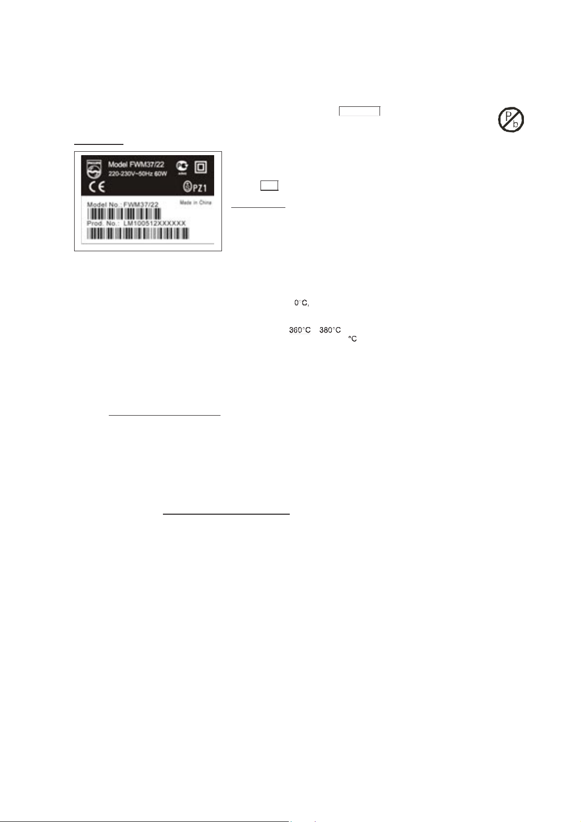
INFORMATION ABOUT LEAD-FREE SOLDERING
Philips CE is producing lead-free sets from 1.1.2005 onwards.
IDENTIFICATION:
Regardless of special logo (not always indicated) one must treat all sets from 1 Jan 2005 onwards, according next rules:
Example S/N:
Bottom line of typeplate gives a 14-digit S/N. Digit 5&6 is the year, digit 7&8 is the week number,
so in this case 2005 wk12
So from 0501 onwards = from 1 Jan 2005 onwards
Im portant note
: In fact also product s of year 2004 must be treated in this way as long as
you avoid mixing solder-alloys ( leaded/ lead -free). So best to always use SAC305 and the
higher temperatures belong to this.
Due to lead-free technology some rules have to be respected by the workshop during a repair:
• Use only lead-free solder alloy Philips SAC305 with order code 0622 149 00106. If lead-free solder-paste is required, please contact
the manufacturer of your solder-equipment. In general use of solder-paste within workshops should be avoided because paste is not
easy to store and to handle.
• Use only adequate solder tools applicable for lead-free solder alloy. The solder tool must be able
o To reach at least a solder-temperature of 40
o To stabilize the adjusted temperature at the solder-tip
o To exchange solder-tips for different applications.
• Adjust your solder tool so that a temperature around
− is reached and stabilized at the solder joint. Heating-time of the
solder-joint should not exceed ~ 4 sec. Avoid temperatures above 400 otherwise wear-out of tips will rise drastically and flux-fluid
will be destroyed. To avoid wear-out of tips switch off un-used equipment, or reduce heat.
• Mix of lead-free solder alloy / parts with leaded solder alloy / parts is possible but PHILIPS recommends strongly to avoid mixed
solder alloy types (leaded and lead-free).
If one cannot avoid or does not know whether product is lead-free, clean carefully the solder-joint from old solder alloy and re-solder
with new solder alloy (SAC305).
• Use only original spare-parts listed in the Service-Manuals. Not listed standard-material (commodities) has to be purchased at
external companies.
• Special information for BGA-ICs:
- always use the 12nc-recognizable soldering temperature profile of the specific BGA (for de-soldering always use the lead-free
temperature profile, in case of doubt)
- lead free BGA-ICs will be delivered in so-called 'dry-packaging' (sealed pack including a silica gel pack) to protect the IC against
moisture. After opening, dependent of MSL-level seen on indicator-label in the bag, the BGA-IC possibly still has to be baked dry.
(MSL=Moisture Sensitivity Level). This will be communicated via AYS-website.
Do not re-use BGAs at all.
• For sets produced before 1.1.2005 (except products of 2004), containing leaded solder-alloy and components, all needed spare-parts
will be available till the end of the service-period. For repair of such sets nothing changes.
• On our website www.atyourservice.ce.Philips.com
you find more information to:
∗
BGA-de-/soldering (+ baking instructions)
∗
Heating-profiles of BGAs and other ICs used in Philips-sets
You will find this and more technical information within the "magazine", chapter "workshop news".
For additional questions please contact your local repair-helpdesk.
SERVICE INSTRUCTION
1. Unplug the AC Power cord and connect a wire
between the two pins of the AC Power plug.
2. Set the AC Power switch to the "on" position (keep the
AC Power cord unplugged!).
3. Measure the resistance value between the pins of the
AC Power plug and the metal shielding of the tuner or
the aerial connection on the set. The reading should be
larger than 4.5 Mohm (For U.S. it should be between
4.2 Mohm and 12 Mohm).
4. Switch "off" the set, and remove the wire between the
two pins of the AC Power plug.
Safety regulations require that after a repair, the set must be returned in its original condition. Pay in particular attention to
the following points:
· Route the wire trees correctly and fix them with the
mounted cable clamps.
· Check the insulation of the AC Power lead for external
damage.
· Check the strain relief of the AC Power cord for proper
function.
· Check the electrical DC resistance between the AC Power
Plug and the secondary side (only for sets which have a AC
Power isolated power supply):
• Check the cabinet for defects, to avoid touching of any
inner parts by the customer.
Page 4

2 - 1
GENERAL
Mains voltage -/98/55
-/98/55
: 120 / 230 V
-/37
-/37
: 120V
Mains frequency : 50 / 60 Hz
:60Hz
Battery for remote : 3V (R03, AAA x 2)
Powe
r consumption Max. : < 37 W (max.)
Standby : < 5 W
ECO : < 1 W
Dimension (W x H x D)
DVD Part
DVD Part
: 208 x 62 x 244 mm
AMP Part : 208 x 57 x 244 mm
Weight : 1.4 Kg
AMP Part : 3.1 Kg
AMPLIFIER
Output power : 2 x 22 W RMS
Subwoofer
Subwoofer
Subwoofer
: 1 x 50 W
Speaker impedance : 2 x 8 ohm
: 1 x 8 ohm
Frequency response : 100 Hz - 20 kHz (±3dB)
: 40 Hz - 180 Hz (±3dB)
Aux input sensitivity : 350 mV (600 ohm)
TUNER - FM SECTION
Tuning range 100kHz : 87.5 - 108 MHz
IF frequency : 10.7 MHz ± 0.02 MHz
Sensitivity : 22 dBf at 26dB S/N
Selectivity : 20 dB at 300kHz
IF rejection : 50 dB
Image rejection : 20 dB
TUNER - AM SECTION
Tuning range MW(9 kHz) : 531 - 1602 kHz
AM(10 kHz) : 520 - 1710 kHz
IF frequency : 450 kHz ± 1 kHz
Sensitivity MW :
Selectivity MW : 16 dB
IF rejection MW : 24 dB
Image rejection MW : 20 dB
DVD / MP3 / CD
Laser Type : Semiconductor
Disc Diameter : 12cm / 8cm
Video Decoding : MPEG-2 / MPEG-1
Signal System : PAL / NTSC
Video S/N : 53 dB (min.)
Composite Video Output : 1.0 Vp-p, 75
S-Video Output : Y - 1.0 Vp-p, 75
C - 0.286 Vp-p, 75
Audio DAC : 24 Bits / 96 kHz
Frequency Response : 4 Hz - 20 kHz (44.1kHz)
4 Hz - 22 kHz (48kHz)
4 Hz - 44 kHz (96kHz)
Digital Output : SPDIF (Sony Philips
digital interface) Coaxial
No. of programmable tracks : 20
Signal-to-noise ratio : 50 dBA
Channel separation : 40 dB (1 kHz)
Total harmonic distortion : < 0.02% (1 kHz)
TFT LCD PANEL
Number of pixels(HXV) : 280x220
Brightness dark room : >150cd/m2
Contrast dark room : 150 :1
LOUDSPEAKERS
2-way bass reflex system
Dimension (W x H x D) : 145 x 230 x 210 mm
Weight : 2.4 Kg each
SUBWOOFER
Dimension (W x H x D) : 80 x 270 x 330 mm
Weight : 4.4 Kg
SERVICE TOOLS
Audio signal disc SBC 429.......................................................................4822 397 30184
Playability test disc SBC 444
...................................................................4822 397 30245
Test disc 5 (disc without errors ) +
Test disc 5A (disc with dropout errors, black spots and fingerprints)
SBC 426/426A.....................................................................4822 397 30096
Burn in test disc (65 min. 1kHz signal at -30 dB level without “pause”)
.....4822 397 30155
anti-static table mat
large 1200x650x1.25mm 4822 466 10953
small 600x650x1.25m 4822 466 10958
anti-static wristband
4822 395 10223
connection box (3 press stud connections, 1MΩ) 4822 320 11307
extendible cable (2m, 2MΩ, to connect wristband to connection box) 4822 320 11305
connecting cable (3m, 2MΩ, to connect table mat to connection box) 4822 320 11306
earth cable (1MΩ, to connect any product to mat or to connection box) 4822 320 11308
KIT ESD3 (combining all 6 prior products - small table mat) 4822 310 10671
wristband tester 4822 344 13999
AVAILABLE ESD PROTECTION EQUIPMENT
Page 5
2 - 2
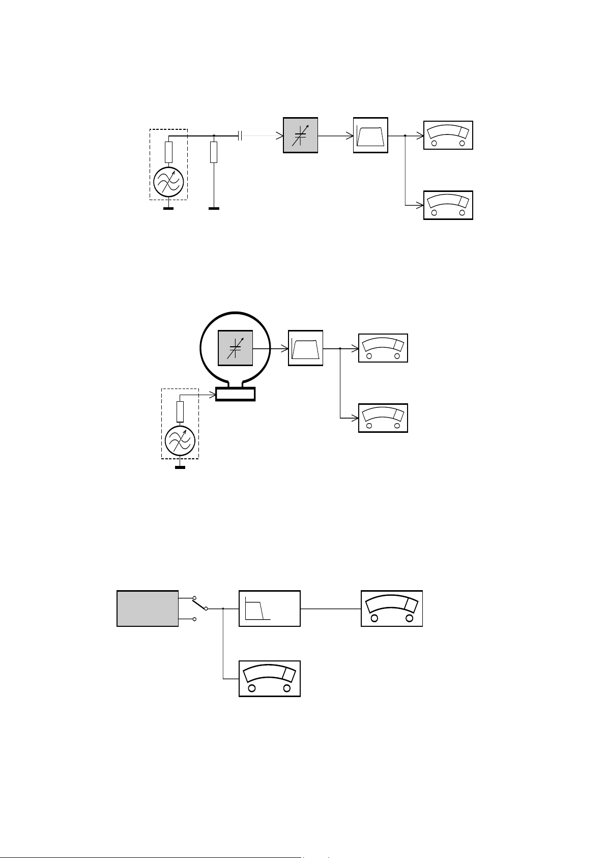
S
ERVICE MEASUREMENT
Bandpass
250Hz-15kHz
e.g. 7122 707 48001
LF Voltmeter
e.g. PM2534
DUT
RF Generator
e.g. PM5326
S/N and distortion meter
e.g. Sound Technology ST1700B
Tuner SW
To avoid atmospheric interference all AM-measurements have to be carried out in a Faraday«s cage.
Use a bandpass filter (or at least a high pass filter with 250Hz) to eliminate hum (50Hz, 100Hz).
Ri=50Ω
Aerial replacement
Capacitor
R=50Ω
Bandpass
250Hz-15kHz
e.g. 7122 707 48001
LF Voltmeter
e.g. PM2534
DUT
S/N and distortion meter
e.g. Sound Technology ST1700B
Frame aerial
e.g. 7122 707 89001
Tuner AM (MW,LW)
To avoid atmospheric interference all AM-measurements have to be carried out in a Faraday«s cage.
RF Generator
e.g. PM5326
Ri=50Ω
Low pass filter 22kHz
L
R
LEVEL METER
e.g. Sennheiser UPM550
with FF-filter
S/N and distortion meter
e.g. Sound Technology ST1700B
DUT
CD
Use Audio Signal Disc SBC429 4822 397 30184 (replaces test disc 3)
L.P.F. = 13
th
order filter 4822 395 30204
Page 6
3 - 1
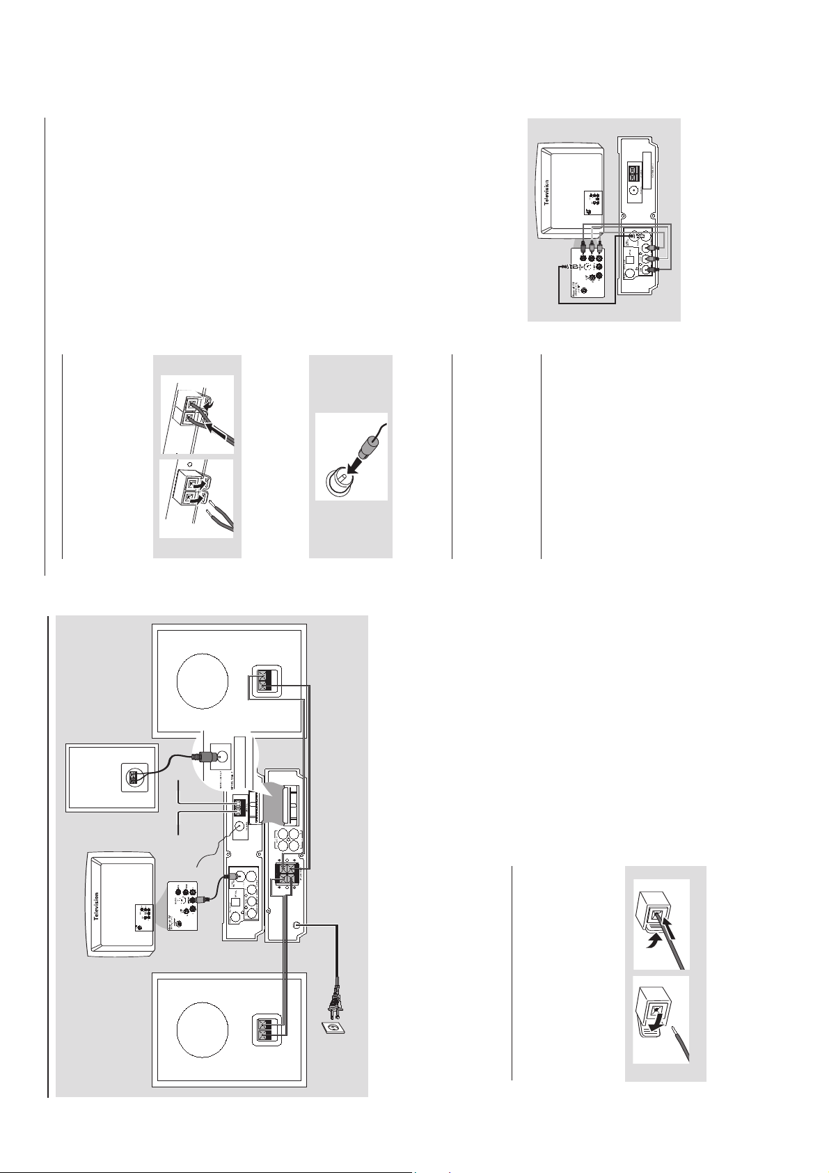
Connections
Connecting antennas
Connect the supplied AM antenna and FM
antenna to the respective terminals. Adjust the
position of the antenna for optimal reception.
AM Indoor Antenna
1
2
Position the antenna as far as possible from a TV,
VCR or other radiation source.
FM Indoor Antenna
For better FM stereo reception, connect an
outdoor FM antenna to the FM AERIAL (FM
ANTENNA) terminal.
Connecting the control cable
Connect the serial port marked “CONTROL
CABLE” at the rear of the DVD player to the
same port at the rear of the power amplifier
with the supplied flat control cable.
Connecting a TV
You must connect a TV to your DVD micro
system in order to view the DVD/VCD playback.
IMPORTANT!
– There are various ways to connect the
system to a TV. You only need to make
one of the best connections, depending
on the capabilities of your TV system.
– If COMPOMENT video output jacks
or S-Video jack is used for video
connection, the system’s Component
setting will need to be set accordingly.
Details are shown under “Video Setup
Page”.
Connect the VIDEO OUTPUT jack to the
video input jack on the TV using a video cable
(yellow).OROption 1
Connect the S-VIDEO output jack to the S-
Video input jack on the TV using an S-Video
cable (not supplied).
OR
Option 2
Use the component video cables (red/blue/
green) to connect the DVD micro system’s
COMPONENT video output jacks to the
corresponding component video input jacks (or
labeled as Pr/Cr Pb/Cb Y or YUV) on the TV.
IMPORTANT!
– The progressive scan video quality is
only possible when using Y Pb Pr and a
progressive scan TV is required. (Proceed
to page 17-18 for detailed Progressive
Scan setup.)
Option 1
Option 2
Note:
–To avoid magnetic interference, do not position
the front s
p
eakers too close to
y
our TV.
CONNECTION AND CONTROLS
IMPORTANT!
– The type plate is located at the
bottom of the system.
– Before connecting the AC power cord
to the wall outlet, ensure that all
other connections have been made.
–Never make or change any
connections with the power switched on.
Connecting the speakers
1
2
Connect the two front speakers to the
SPEAKERS (8ohm) terminals with two speaker
cables. Right speaker to “R” and left speaker to
“L”, red wire to “+” and silver wire to “-”. Fully
insert the stripped portion of the speaker wire
into the terminal as shown.
A
B
Connections
Connect the passive subwoofer to the
WOOFER OUT (8ohm) terminal with the supplied
subwoofer cable by matching the plug types.
Notes:
– Ensure that the speaker cables are correctly
connected. Improper connections may damage the
system due to short-circuit.
–For optimal sound performance, use the supplied
speakers.
– Do not connect more than one speaker to any
one pair of +/- speaker jacks.
– Do not connect speakers with an impedance
lower than the speakers supplied. Please refer to
the SPECIFICATIONS section of this manual.
AC power cord
Speaker
(right)
Speaker
(left)
AM antenna
FM
antenna
Subwoofer
Page 7
3 - 2
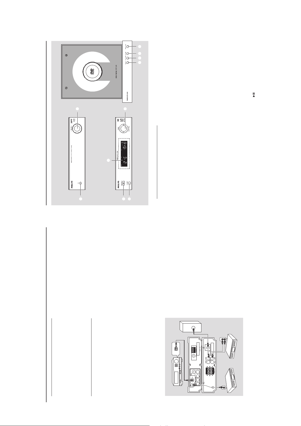
Functional Overview
DVD player and power amplifier
1
ECO POWER/STANDBY ON B
– to switch the system on or to Eco power/normal
standby mode.2IR SENSOR
– point the remote control towards this sensor.
3
Control knob
4 / ¢
Disc .......................press the control knob to the
left/right to skip to the previous/
next chapter/title/track.
Tuner....................press the control knob to the
left/right to tune to a higher/
lower radio frequency.
.................................press and hold, then release the
key to start automatic search for
a radio frequency downward/
upward.
PROGRAM
DVD/VCD/CDpress the control knob upward
to enter the program menu.
MP3/WMA-CD
.................................press the control knob upward
to add/delete a programmed
track to/from the program list.
Picture CD........ during playback, press the
control knob upward to select a
slide show mode.
Tuner ....................press the control knob upward
to program preset radio stations.
REPEAT•STEREO
Disc .......................press the control knob
downward to repeat a track or
disc.
FM.......................... press the control knob
downward to set stereo or
mono sound mode.
4
Display
– shows the current status of the DVD player.
5
SOURCE
– selects the respective sound source: DVD/
AUX1/AUX2/TUNER.
– switches the system on.
6
PRESET/
– Disc: starts or interrupts disc playback
– TUNER: selects a preset radio station
0
9
5 6 7 8
4
3
1
2
THEATRE
ECO POWER
CONNECTION AND CONTROLS
Connections
Connecting the power cord
After everything is connected properly,
plug in the AC power cord to the power
outlet.
Never make or change any connection with the
power switched on.
Connecting additional
equipment
IMPORTANT!
– Some discs are copy-protected. You
cannot record the disc through a VCR or
digital recording device.
–When making connections, make sure
the colour of cables matches the colour
of jacks.
– Always refer to the owner’s manual of
the other equipment for complete
connection and usage details.
DIGITAL IN
CD Recorder
(for example)
Digital amplifier
(for example)
VCR
(for example)
AUDIO IN
L R
DIGITAL IN
OPTICAL
AUDIO
INPUT
Active subwoofer
(for example)
Viewing and listening to the playback of
other equipment
Connect the system’s AUX IN (R/L) jacks to
the AUDIO OUT jacks on the other audio/
visual device (such as a TV, VCR, Laser Disc player
or cassette deck).
Before starting operation, press AUX on the
remote repeatedly in order to activate the input
source (AUX1 or AUX2).
Connecting an active subwoofer Connect the DVD micro system’s WOOFER
OUT jack to the AUDIO INPUT jack on an
active woofer (not supplied).
Recording (digital)
Connect the system’s DIGITAL OUT
(COAXIAL or OPTICAL) jack to the
DIGITAL IN jack on a digital recording device
(such as DTS-Digital Theatre compatible, with
Dolby Digital decoder).
Before starting operation, set SPDIF
according to the audio connection. (See “SPDIF
Setup”).
Connecting a digital amplifier
Connect the DIGITAL OUT (COAXIAL or
OPTICAL) port to the coaxial/optical input
jack of a digital amplifier with a coaxial/optical
cable (not supplied) for superior digital sound
effect.
Page 8
3 - 3
English
Functional Overview
@
TU +/- ( / )
Tuner
– press to tune to a lower/higher radio frequency
gradually.
– press and hold, then release the key to start
automatic search for a radio frequency
downward/upward.
Disc
– searches backward/forward in a disc at different
speeds.#VOLUME +/-
– adjusts the volume upward/downward.
– adjusts the hours and minutes in clock/timer
setting mode.
– switches the set timer ON or OFF.
$
CH +/- ( / )
– Disc: skips to the previous/next chapter/title/
track
– Tuner: selects a preset radio station.
%
– starts or interrupts disc playback.
^
9
– stops disc playback or erases a program.
&
DISC/TUNER/AUX
– selects the respective sound source for DVD/
TUNER/AUX1/AUX2.
– exits P-SCAN (progressive scan). (for DISC
only)*SLEEP/TIMER
Standby mode
– sets a time for switching on the system
automatically.
Power-on mode
– sets the sleep timer function (auto off).
(
CLOCK
Standby mode
– sets the system clock.
Playback mode
– displays the system clock.
)
DIM
– selects different levels of brightness for the
dis
p
la
y
screen in standb
y
mode.
¡
SUBTITLE
– selects a subtitle language.
™
ANGLE
– selects a DVD camera angle.
£
DISPLAY
– displays information on TV screen during
playback
AUDIO
for VCD
– sets Stereo, Mono-Left or Mono-Right sound
mode.
for DVD
– selects an audio language.
∞
A-B
– repeats playback of a specific section on a disc.
§
MODE
– selects various repeat modes or the shuffle play
mode for a disc. SLOW
– selects different slow playback modes for a
VCD/SVCD/DVD.
DBB
– enables or disables bass enhancement.
ª
SURROUND (unavailable for this
version)
– selects surround (Dolby Digital, DTS-Digital
Theatre Systems or VSS-Virtual Surround
Sound) or stereo sound effect.ºVOL.SEL (unavailable for this version)
– selects different speaker modes.
DSC
– selects different types of preset sound equalizer
settings (CLASSIC, JAZZ, POP or ROCK).¤LOUDNESS
– enables or disables automatic loudness
adjustment.
≤
≥
•
⁄
CONNECTION AND CONTROLS
7
BAND/9
– Disc: stops disc playback or erases a program.
– TUNER: switches between AM and FM.
8
OPEN•CLOSE
– opens or closes the disc compartment.
9
VOLUME -/+
– adjusts the volume upward/downward.
– adjusts the hours and minutes in clock/timer
setting mode.
– switches the set timer ON or OFF.
0
n
– connect a headphone
Functional Overview
Remote control
1
B
– to switch the system on or to Eco power/normal
standby mode.20
– opens or closes the disc compartment
3
Numeric Keypad (0-9)
– inputs a track/title/chapter number of the disc.
– inputs the number of a preset radio station.
4
PROG
– DVD/VCD/CD: enters the program menu.
– MP3/WMA-CD: adds/deletes a programmed
track to/from the program list.
– Picture CD: during playback, to select a slide
show mode.
– Tuner: programs preset radio stations.
5
GOTO/ST
– Disc: fast searches in a disc by entering a time,
title, chapter or track.
– FM: sets stereo or mono sound mode.
6
SYSTEM (disc mode only)
– enters or exits the system menu.
7
DISC MENU (disc mode only)
–DVD/VCD: enters or exits the disc contents
menu.
– VCD2.0: switches the playback control mode on
or off .
– MP3/WMA: switches between Album and Filelist.
8
///
– selects an item in a menu.
–moves an enlarged picture up/down/left/right.
9
OK
– confirms a selection.
0
ZOOM
–DVD/VCD/Picture CD: enlarges or reduces a
picture or active image on the TV screen.!MUTE
– disables or enables sound output.
1
3
6
8
0
!
%
&
*
¡
∞
ªº§
™
(
2
5
7
9
!
$
^
)
¤
⁄
≥
£
#
4
≤
•
Page 9

3 - 4
The aspect ratio of the screen cannot be
changed even though you have set the TV
shape.
No sound or distorted sound.
The micro DVD player does not start
playback.
The DVD micro system does not respond
w
hen the buttons are pressed.
Cannot activate some features, such as
Angles, Subtitles, or multi-language
Audio.
Considerable noise in radio broadcasts.
Sound cannot be heard or is of poor
quality.
The aspect ratio is fixed on the DVD disc.
Depending on the TV, it may not be possible to
change the aspect ratio.
Adjust the volume.
Check that the speakers are connected
correctly.
Replace the speaker cables.
Disconnect the headphones.
The system is in pause, slow motion or fast
forward/reverse mode, press PRESET/ (or
on the remote) to resume normal play
mode.
Insert a readable disc with the playback side
facing down.
Check the disc type, colour system and regional
code. Check for any scratches or smudges on
the disc.
Press SYSTEM MENU to turn off the setup
menu screen.
Cancel the parental control rating function or
change the rating level.
Moisture has condensed inside the system.
Remove the disc and leave the system turned
on for about an hour.
Disconnect the power plug from the outlet and
insert again.
Multi-language sound or subtitle is not
recorded on the DVD.
Changing the language for the sound or subtitle
is prohibited on the DVD.
The features may not be available on the disc.
Tune in to the correct frequency.
Connect the antennas.
Fully extend the FM wire antenna. Position for
best reception and secure to a wall.
Connect an outdoor FM or AM antenna.
Adjust the direction and position for best
reception.
Place the antenna farther away from any
equipment that may be causing the noise.
Increase the distance between the system and
your TV or other equipment.
TROUBLESHOOTING
WARNING
Under no circumstances should you try to repair the system yourself, as this will invalidate the
warranty. Do not open the system as there is a risk of electric shock.
If a fault occurs, first check the points listed below before taking the system for repair. If you
are unable to remedy a problem by following these hints, consult your dealer or Philips for
help.
Troubleshooting
No power.
No picture.
Distorted or poor picture.
Completely distorted picture or black/
white picture.
Check if the AC power cord is properly
connected.
Press STANDBY ONB on the top of the DVD
micro system or B on the remote to turn on
the power.
Check if the TV is switched on.
Check the video connection.
Press SOURCE on the top of the DVD player
repeatedly to select “DVD” or press DISC on
the remote.
Set your TV to the correct Video In channel. This
channel is usually near channel 00. Or, you may
have a button on the TV remote control that
selects Auxiliary or A/V IN channel. See your TV
owner’s manual for details. Or, change channels
at the TV until you see DVD screen on the TV.
If the progressive scan feature is activated but
the connected TV does not support progressive
signals or the cables are not connected
accordingly, see page 17-18 for proper
progressive scan setup or deactivate the
progressive scan feature as below:
1) Turn off your TV progressive scan mode or
turn on to interlaced mode.
2) Press SYSTEM on the remote to exit the
system menu and then DISC to exit progressive
scan.
Sometimes a small amount of picture distortion
may appear. This is not a malfunction.
Clean the disc.
TV has a colour system standard. If the disc’s or
DVD system’s colour system is different than
your TV’s colour system, the picture may be
distorted or colourless.
Problem
Solution
Page 10

3 - 5
The remote control does not function.
The display is dark.
Low hum or buzz sound.
Low bass response.
Unable to select Progressive Scan
Select the correct source (DISC or TUNER, for
example) before pressing the function button.
Point the remote control at the remote sensor
of the unit.
Reduce the distance to the player.
Remove any possible obstacles.
Replace the batteries with new ones.
Check that the batteries are loaded correctly.
Press DIM again.
Place the DVD micro system as far away as
possible from electrical devices that may be
causing interference.
Check all speakers for correct polarity.
Check that the output of the video signal is
switched to 'Ypbpr'.
TROUBLESHOOTING
Page 11

5 - 1
5 - 1
SOFTWARE VERSION AND UPGRADING
Page 12

5 - 25 - 2
SET BLOCK DIAGRAM
Page 13

5 - 3 5 - 3
SET WIRING DIAGRAM
Page 14

6 - 1 6 - 1
CIRCUIT DIAGRAM - VFD / KEY BOARD ASSEMBLY
MCD-7
+5V-2
0
R712
R702
47K
+5V
C702
104
G1G2G3G4G5
C701
47uF
VFD701
NE-1300CD-3.G
VF11VF12S33S24S15S156S167S48S59S610S711G212G313G414G115G516NC17G918G619G720G821S822S923S1024S1125S1426S1327S1728S1829S1930S1231VF232VF2
33
S1S2S3S4S5S6S7
G6G7G8
39
40
41
42
43
44
45
46
47
48
49
50
51
52
G5
G4
G3
G2
G1
Vdd
LED5
LED4(BBE)
LED3(POWER)
LED2(FANCT)
LED1(7507RST)
Vss
OSC
37
38
G8
G7
G6
SW11SW22SW33SW44DOUT5DIN6IC7CLK8STB9KEY110KEY211KEY312KEY4
S8
S9
G10
G9
35
36
S20/G9
S19/G10
IC701
uPD16311
S10
C704
104
-24V
34
33
VEE
S11
S18
32
Vdd
S12
S13
S14
S15
S15
S16
S17
S18G5G6
S16
S17
S13
S14
G7
G8
G9
G4
G3
G2
G1
G10
S701
30
S17/G1231S18/G11
S1327S1428S1529S16
S12/K S12
S11/K S11
S10/K S10
S9/KS9
S8/KS8
S7/KS7
S6/KS6
S5/KS5
S4/KS4
S3/KS3
S2/KS2
S1/KS1
Vdd
26
25
24
23
22
21
20
19
18
17
16
15
14
S12
S11
S10
S9
S8
S7
S6
S5
S4
S3
S2
S1
REMOTE
D702 4148
S2
S3 KS 3
S1
+5V
K4
K3
R706 33K
R707 33K
K2
K1
R708 33K
13
STB1
CLK
DATA
33K
R705
Vcc
GND
REM
D703 4148
D701 4148
SW701
TACT(STBY)
3
+5V
2
V-GND
1
REM
KS2
R704
15/0.5
VF2
R703
2.2/0.5
10K
R709
4K7
R701
K1
K2
K3
K4
KS2
10K
R710
K1
K2
K3
K4
KS3
STB1
DATA
CLK
V-GND
REM
+5V
GND
VF1
VF2
-24V
CN701
2.0/3P
CN702
1
2
3
4
5
6
2.0/5P
CN703
6
5
4
3
2
1
2.0/5P
3
2
1
CN704
1
2
3
4
5
6
2.0/6P
REP
3
4
+SKIP
COM
PRE
2
SEARCK
SEARCH5PLAY/PAUSE
NEXT
SW1501
FUNC)
T(
SW1502
T(PLAY)
SW1503
T(ST OP)
SW1504
T(OP/CL)
MEM
1
-SKIP
6
KEY4-2
KEY3-2
KEY2-2
KEY1-2
SW706
4SW
gn d
KS3-2
KEY4-2
KEY3-2
KEY2-2
KEY1-2
MCD-14
KEY1-1
KEY2-1
KEY3-1
KEY4-1
KS2-1
CN1501
1
2
3
4
5
6
2.0/5P
MCD-15
CN1401
1
2
3
4
5
2.0/5P
Page 15

6 - 26 - 2
LAYOUT DIAGRAM - VFD / KEY BOARD ASSEMBLY
Page 16

7 - 17 - 1
CIRCUIT DIAGRAM - TUNER BOARD
AM ANT
C2 7
203
R7
100k
T205B BL ACK
6
5
C4
C2 6
10uF
223
R1 9 10K
0
1.2
GND2
REG
C3 4
102
C3 0
103
C4 8
203
5
AOUT 2
CE
R1 6
1K
R3 0
10
6T 5
C2 5 203
4.4
RF OUT
AM OS C
4.5
T303B
L3
C4 6
100u F
AIN2
DI
R1 4
1K
ANT 1
C3
47P
1
2
34
C4 3
18P
C2
30P
6T 5
R3
47K
C3 8
36P
L4
C1
47P
D3 I384
R2 9
10
C2 4
223
R6
47K
C4 1
102
C3 7
7P
RF IN
AM RF
123456789101112
1
2
C3 9
5P
34
C3 2
102
R2
47K
D2
SCV 220
0.9
1.2
VS S
X-OUT
X1
4.5M
C4 0
36P
X-IN
12345678 9101112
BO 5
C1 7
100P
4.4
VCC2
VCC1
4.5
R5
47K
D1
SCV 220
C3 6 3 P
C4 7
223
PD2
CL
R1 5
1K
C4 2
501
3.7
FM OS C
FM IF OUT
2.2
CF 1
10.7M
C2 8
103
R1 2
1K
L2
5T 5
C2 1 18P
0.1
0
PD1
IC 4
DO
R1 8
1K
C3 3
103
1.2
DET OUT
GND1
MPXI N
IC 3 L A 1823
IF BUFF
4.5
1K
CF 2
10.7M
C6
3.3u F
R1 3 1K
R2 3
2.2K
AIN1
LC 72130
BO 1
C1 8
100P
C3 5
222
C1 1
4.7u F
R8
100K
C2 2
223
AOUT 1
BO 2
1.2
4.5
C2 9
103
R OUT
ST
C1 3
100u F
C8
0.22u F
C9
0.33u F
C3 1
103
1.2
L OUT
4.5
C1 4
100u F
VDD
BO 3
4.5
FM/A M
AMIF OUT
1
2
34
T403B
DZ 2
5V 1
FMIF IN
1.2
5
FM IN
BO 4
R1 7 1K
R9
3.3K
AM IN
IO 1
4.5
1.2
C1 9
102
C1 0
3.3u F
ST/M O
AMIF IN
C1 2
0.47u F
CF 3
450J
L1
10uH
R1 0 100
131415161718192021222324
C2 0
R2 0 10K
C4 4
15P
131415161718192021222324
0.1 3 .7
R2 4 330
IF IN IO2
AGC DE T
102
1
2
34
T5118
R36
2.2K
C50
682
C4 5
470P
C4 9
103
R2 1
10K
5
R1 1
100
C1 6
100u F
C51
682
2.2K
R35
C1 5
100u F
R2 5
1.5K
Q1
9014
R2 7
220
C5
3.3u F
DZ 1
5V 1
R?
82K
C2 3
223
R2 6
1.5K
9014
R2 8
220
Q2
R2 2
180
C7
3.3u F
R1
47K
R34
100K
R4
47K
R?
100K
Q3
9014
DO
CL
DI
CE
GND
J1
1
2
3
4
CON4
J2
1
2
3
4
5
CON5
L OU T
GND
R OU T
9V
Page 17

7 - 2 7 - 2
LAYOUT DIAGRAM - TUNER BOARD
Page 18

8 - 18 - 1
CIRCUIT DIAGRAM - DVD BLOCK
CN807
1
2
3
4
5
6
7
1
2
CN805
MCD700-5
1
2
CN501
DS-STB2
DS-STB1
DS-DAT
DS-CLK
REM
+5V
DGND
DGND
+5V
PGND
+5VLED
GNDLED
MCD700-
ROT-A
ROT-B
103
R825 10K
C837
LED501 LED(BLUE)
2 1
R901 2K2
10K
C857
104P
R826
8
C838
103
C858
220UF/10V
R828 10K
R827 10K
L802
22UH
C859
10000uF/16V
MCD700-4
CLOSSW
1
GNDSW
2
OPENSW
3
CN401
D803
4148
C860
104
R850
3.3K
D804
4148
REMOTE
C879
100UF/16V
L803
IN5822
R851
1K
SW402
SW(CLOSE)
SW401
SW(OPEN)
CD-REM
DGND
220UH
D801
JP802
0
104P
C878
12 34
12 34
2
101
C834
101
C849
C839
OUT
GND
Vo
GND
Vref4ON
3
101
C854
IN
C877
Vi
5
U802
LM 2576
2
1
CN601
2P/2.5
101
R835
R834
R831
R841
U803
7805
47UF/25V
1
M+
M-
101
C855
R836
R847
47K
4001
D601
100
100
100
100
100
R858
120/2w
R848
1K
Q804
8050
4001
D602
1K
R601
R844
10K
Q601
33K
4001
D603
8550
CD-REM
100
R849
STB3
R857
MCD700-6
33
P5.6
34
P5.7
35
P6.0
36
P6.1
37
38
39
40
41
42
43
44
P6.2
P6.3
P0.0
P0.1
P0.2
P0.3
P0.4
P0.5
DS-STB1
DS-DAT
DS-CLK
ROT-A
ROT-B
1
10UH
L807
DVD-ON
R865
1K
F801
F1.5A/125V
12
+-
M
M601
MOTOR(RF-370C-13470)
32
2
C848
220uF
C861
104
STANDBY
R832 100
P5.5
P1.1
MUTE
OTG1
OTG2
D809
4148
R833 100
R815 100
R816 100
30
29
28
P5.3
P5.2
P5.431P5.1
VDD5P1.34P1.23P1.0
DVD-CH
C808
104
C883
1000u/25v
J701
RCA_1P(YELLOW)
MCD700-11
TUNE-ON
OTG3
R829 100
R817 100
P5.027P4.726P4.625P4.524P4.4
TEST
VSS6XOUT7XIN
XTIN
9
8
10
X802
4.19MHz
R809
10K
C819
C820
30P
30P
D811 4001
D812 4001
C862
3300uF/35V
C843 101
DTS-CE
23
RESET
XTOUT
11
10uH
L1101
10uH
L1102
331
C1102
P4.3
P4.2
P4.1
P4.0
P3.0
P3.1
P2.0
P2.1
P2.2
P2.3
X801
32.768KHz
C816
15P
+ACAC
22
21
20
19
18
17
16
15
14
13
12
U804
3S9228
4148
D807
C815
15P
R1104
100
CN1101
CN806
PLL-CE
100
R806
DTS-CL
DTS-DATA
CDSTB
CDCLK
CDDATA
DVD-ON
MCURESE
-
BD801
C866
331
C1102
+5V
R814
22K
SP
K
C821
10uF
104
R1101
100
R1103
GND
12345
CD-CLK
CD-DATA
DVD-CH1
T
G1SP2G
100
R1102
33
123
CD-STB
+5VA
C867
CD-REM
PLL-CLK
R802 100
R807
10K
DVD-CH
331
O
OPTICAL
3
104
C1104
6
PLL-DATA
CD-STB
CD-CLK
R823 100
R805 100
R822 100
100
R845
R812
10K
701
123456789
CN809
DGND
TUNE-ON
CD-DATA
DVD-CH1
R830
R824 100
101
C840
OTG3
101
C876
PLL-CE
10K
C804
104P
OTG2
101
C875
PLL-CLK
1
OTG1
PLL-DATA
C807
220uF
101
C874
+10V
10uH
L801
C850 101
10
TUNER-L
TUNER-R
100
SCL
R804
23
Q802
8550
1
32
R840
1K
R842 100
Q801
8050
R820
47K
C841 101
SDA
101
C828
PLL-DAT A
U807 24C02
1
2
3
SCL
101
C827
CD-STB
C803 101
A0
A1
A2
GND4SD A
CD-CLK
C801 101
C822
104
PLL-CE
PLL-CL K
C851 101
SD A
R843 100
C802 101
R821
CD-DATA
+12V
4K7
Vdd
TEST
SCL
R859
R860
4.7K
C812
9014
TUNE-ON
101
1K
Q807
8550
STANDBY
101
C811
STB3
C880
104
C881
100UF
Q806
8
7
6
5
STB3
C809
101
CD-R
CD-L
MUTE
STB3
ROT-A
ROT-B
DGND
CD-L
CD-R
DGND
SCL
SDA
+12V
TUNER-L
TUNER-R
STANDBY
+5VA
MUTE
AU-L
OTG1
AU-R
OTG2
DGND
OTG3
CN802
CN803
OTG1
OTG2
CN903
3
2
1
4.7K
OTG3
Vcc
SP
GND
GND
CN902
R861
VIDEO
2
1
GND
JACK901
1
2
3
4
5
6
7
S-V IDEO
JACK902
1
2
3
4
5
6
L901 9u
L902 9u
L903 9u
L904 9u
L905 9u
L906 9u
L907 9u
L908 9u
L909 9u
L910 9u
RCA3P
MCD700-9
SCSYGND2
CVBS
SP
GND
+5V
1
10
2
VIDEO
C864
102
C865
AC11V
AC11V
102
L808
L809
L810
RED
GREEN
BLUE
CN901
123456789
CN811
2
1
5uH
CDR
CDL
CDG
B_MUTE
CN810
CN804
-24V
VF1
VF2
4
3
2
1
3
2
1
CN801
VF2
CLK
VF1
DATA
~10V
STB3
~10V
VIDEO-G
ROT-A
VIDEO
ROT-B
-24V
TUNER-R
CD L
CD R
GND
SCL
SD A
+12V
TUNER-L
GND
STANDBY
+5V
MUTE
AU-L
OTG1
AU-R
OTG2
GND
OTG3
D810
4148
10
11
12
13
14
15
16
17
18
19
20
21
22
23
24
25
26
27
28
29
30
5uH
5uH
1
2
3
4
5
6
7
8
9
C882
4.7UF
123
Page 19

8 - 2 8 - 2
LAYOUT DIAGRAM - DVD BLOCK
Page 20

9 - 1
9 - 1
CIRCUIT DIAGRAM - AMP BLOCK
CN101
3P
3P
RCA-407
1
2
3
4
5
6
7
8
9
10
11
12
13
14
15
16
17
18
19
20
21
22
23
24
25
26
27
28
29
30
CN113
1
2
3
3CN1600
2
1
J200
PHONE3.5
6
5
G2
4
3
2
G1
1
J103
~12.5V
~12.5V
VF2
TFT-VCC
VF1
VIDEO
RO T-A
VIDEO-G
RO T-B
-28V
DGND
CD-L
CD-R
GND
SCL
SD A
+12V
TU-L
TU-R
STANDBY
MUTE
AGND
30P
RO T-A
RO T-B
DGND
EC O
GND
VCC
MCD700-2
1
2
L
3
4
5
R
8
7
6
11
10
9
R150 10K
R155
10K
GND
LO-H
R151
10K
R154
10K
MU-H
RO -H
GND-H
D201
4001
D202
4001
R153
47K
R157
47K
CN200
COM4
GND
AUX1-L
AUX1-R
R152
47K
R156
47K
AUX2-R
4
3
2
1
AUX2-L
CD-R
TU-R
CD-L
VF1
VF2
~10V+
~10V-
-28V
DGND
ENCODER301
ENCODER
TU-L
SD A
SCL
+12V
MUTE
STANDBY
C163
100uF/35V
MCD700-3
RO T A
3
A
2
1
C301
103
RO T B
RO T G
B
G
R139
15 1/4W
C302
103
R149
10K
2.2uF
C135
C134 2.2uF
C131104(M)
14
12
L IN413L IN3
LOUD_L
C1382.2uF
C136 2.2uF
C137 2.2uF
C139 2.2uF
C128 104(M)
11
7
6
R IN48R IN39R IN210R IN1
R OUT
LOUD_R
C123 10uF
5
R IN
C118 272(M)
4
TREB_R
3
L IN215L IN116L IN17L OUT18BIN_L19BOUT_L20BIN_R21BOUT_R22OUT_R23OUT_L24DGND25DATA26CLK27REF
104(M)
104(M)
C140 2.2uF
C141 2.2uF
C132 10uF
C129 104(M)
R127
C120
C125 104(M)
5K6
R126
C116
5K6
C111 10uF
C112 10uF
F103 F2A/250V
D301
4001
GND
D302
4001
ZD107
3V0
CN301
D103
4001
3P
1
2
3
!
R113
2.2 1/ 4W
R114
2.2 1/ 4W
D106
4001
DGND
~21V
~21V
~12.5V
~12.5V
1234567
~2.5 V
8
~0V
7
~2.5 V
6
~21V
5
~0V
4
~21V
3
~16.5V
2
~16.5V
1
~16.8V
3
~0V
2
~16.8V
1
2.2V
0V
2.2V
8
CN111
8P
272(M)
C114
2
AGND
TREB_L
R135 1K
!
1
28
R132 1K
CN109
5P
VDD
C107
47uF
C109
22uF
U104
PT2314
R120
330 1/4W
MUTE
12345
R130
47K
!
AC IN
R129
47K
47K
R101
47K
D108
4001
D109
4001
R110
47K
GND
Q101
2 3
1
R105
47K
C105
22uF
+21V
-21V
B834
R106
4K7
Q102
8050
IN1
8
R166
R160
4K7
47uF/35V
47K
OUT-EL
OUT-ER
C115
7
U103
7812
GND
R162
47K
IN
GND
C122
IN2
6
R161
4K7
OUT
47uF
C101
4700uF/35V
C102
4700uF/35V
U105
TDA7264
-Vs
5
C130
10uF/50V
Q106
8050
DB101
RS808
TDA7264
MUTE
4
MUTE_AMP
R109
15K
+ACAC
F102
F4A/250V
!
C157
~16.5V-
3
104(M)
R147
AGND
+Vs
OUTPUT2
2
OUT-R
C145
104(M)
2.2/0.5W
R134
15K
R115
47K
Q105
8050
-
F101
F4A/250V
!
~16.5V+
CN106
3P
123
R112
22K
47uF
R146
C103
1
2.2/0.5W
OUT-L
OUTPUT1
C178
332
OUT-L
C179
332
+12V
OUT-R
4K7
4K7
R102
R181
D107
4148
R182
22K
MCD-1
4 3
4 3
JKB7525_01
R133
220 1/2W
D105
4148
R136
1K
C152
1uF
8
7
6
5
C151
47uF
R180
120
R111
1K
Q103
8050
L105
JKB7525_01
L104
ZD108
5.1V
VDD
MUTE
OUT2
BIAS
IN2
U106
PT2309
Q107
8550
C176
221
12
12
C177
221
OUT1
IN1
GND
FAN
AGND
OUT-R
OUT-L
R103 1K
C154
47uF
C150
220uF
J104
R158
10K
C153 1uF
1
2
3
4
R159
100K
C149
220uF
PST-416(UP RED DOWN BLACK )
HP-MUTE
H-OUT L
H-OUT R
AGND
CN103
4P
CN108
2P
4
3
2
1
1
2
Page 21

9 - 2
9 - 2
LAYOUT DIAGRAM - AMP BLOCK
Page 22

10 - 1
10 - 1
CIRCUIT DIAGRAM - DVD MPEG BOARD
MPEG board is not repaired,program for referrence only.
[1]
[1]
[1]
[1]
[1,2,3,5]
[1]
[1,2]
[2]
[2]
[2]
[2]
[2]
ACLK
ALRCK
ABCK
ASDAT0
ASDAT1
ASDAT2
TP66
TP65
TP64
TP63
+12V
-12V
+12V1
DV33[1]
VCC
VCC_AUDIO[1]
GND
MIC1
MIC_EN
ASPDIF
ASDAT[0..2][2]
ACLK
ABCK
ALRCK[2]
MUTE_DAC
RESET#[2]
ML[4]
MR[4]
DEMP[2]
AMDAT
REST_CS[2]
SCL[2,3]
SDA[2,3]
VSCK[2]
VSDA[2]
FAN[2]
R138 33
R139 33
R142 33
R143 33
R144 33
R145 33
SACLK
SBCLK
SLRCK
SDAT0
SDAT1
SDAT2
GND
4
+12V
ASDAT[0..2]
MUTE_DAC
RESET#
ML
MR
AMDAT
REST_CS
SCL
SDA
VSCK
VSDA
FAN
MIC2
GND
R176
0
+12V
-12V
+12V1
DV33
VCC
VCC_AUDIO
GND
MIC1
MIC_EN
ASPDIF
ACLK
ABCK
ALRCK
DEMP
SACLK
SLRCK
SBCLK
SDAT0
SDAT1
SDAT2
J2
1
2
3
4
4x1W/HOUSING
DIP4/W/H/P2.0
FAN
J21
TJC3-8A
1
2
3
4
5
6
7
8
9
10
GND
A_D5V
A_D5V
A_D5V
SDA
GND
GND
SCL
C45
R212
NC/10k
A_D5V
+
CE11
0.1uF
47uF/16V
R211 OPEN
R210 0
R80
R209 OPEN
R83 0
R20 0
R208 0
R95 OPEN
Q34
NC/9014,SMD
VCC
VCC_AUDIO
SACLK
SBCLK
AMDAT
VCC_AUDIO
SLRCK
1:D/ACE2746(U24)
R128,R210,R145,R142,R204,R205,R206,R207,R208,CE71,CE46(OPEN)R209=0,R129=10,R198=R199=33,CE40=100uF/10V
2:D/ADA1196/WM8746(U24)
R209,R142,R198,R199,R129,R207,R208,CE71,CE46(OPEN),R128=10
L1
FB
A_D5V
SACLK
SBCLK
SLRCK
SDAT0
SDAT1
SDAT2
MODE
R12 0
0
U18
1
VL
2
MCLK
3
SCLK
4
SDATA
5
VA
6
GND
7
LRCK
8 9
DIV DIF
NC/CS5333
U10
WM8746/DA1196
1
DVDD
2
MCLK
3
BCLK
4
LRCK
5
DIN0
6
DIN1
7
DIN2
8
MODE
9
MUTE
10
LRCIN2
11
DGND
12
ML/I2S
13
MC/IWL
14 15
MD/DM AVDD2
R_GND
RST
VQ
LIN
RIN
FIL+
TST
AVDD1
OUT0R
OUT0L
AGND2
OUT1R
OUT1L
AGND1
OUT2R
OUT2L
GR0
GR1
GR2
CAP
16
15
14
13
12
11
10
I2SFORMAT
28
27
26
25
24
23
22
21
20
19
18
17
16
4
L_IN
R_IN
VCC_AUDIO
+
+
C21
CE55
1U
1U
+12V
CB78
0.1uF
R210=R145=R204=R205=R206=0,CE40=10uF/16V
DAC_MR
DAC_ML
DAC_SR
DAC_SL
DAC_LFE
DAC_CENT
CAP
CE48
+
CB75
0.1uF
100uF/16V
HARDWAREMODE
MIC2
R93
NC/470
J22
1
2
NC/2.54mmTJC3-2
R213
NC/4k7
R214
NC/4K7
VCC
+
Q35
NC/9015,SMD
CE59
NC/10u/16V
TP81
TP82
CE5
+
OPEN/10uF/16V
FAN
DV33
R118
OPEN/4.7k
MIC_L
MIC_R
C64 2200pF
C66
2200pF
R112
OPEN/1k
C60 2200pF
VREF
C62
VREF
2200pF
VREF
VREF
C68
2200pF
VREF
C72 2200pF
VREF
1
R110
20k
R116
5.1k
10k
R193
R123
20k
R128
5.1k
10k
R194
R132
20k
R136
5.1k
3.9k
R198
R146
20k
5.1k
R148
10k
R197
R152
20k
R154
5.1k
10k
R196
R158
20k
R164
5.1k
10k
R195
Q18
OPEN/2N3904
SOT23
2 3
C59 220pF
GND
U13A
-
2
+
3
NJM4558OPA
8 4
+12V
C61 220pF
GND
U13B
-
6
+
5
NJM4558OPA
8 4
+12V
C63 220pF
GND
U15A
-
2
+
3
NJM4558OPA
8 4
+12V
C65 220pF
GND
U15B
-
6
+
5
NJM4558OPA
8 4
+12V
C67 220pF
GND
-
2
+
3
NJM4558OPA
8 4
+12V
C69 220pF
GND
-
6
+
5
NJM4558OPA
8 4
+12V
1
7
1
7
U16A
1
U16B
7
CE31
+
OPEN/10uF/16V
CE57
+
100uF/16V
R119
R131
47k
R141
47K
R151
47K
47k
R167
R157
47k
47k
ML
MR
SL
SR
CENT
SUB
VREF
R117
100
R129
100
R137
100
R204
N2
OPEN/0
C97 100pF
R206
N1
OPEN/0
C98 100pF
R205
N6
OPEN/0
C99 100pF
N5
R149
100
C100 100pF
N4
R155
100
C101
100pF
N3
R165
100
C102 100pF
R85
OPEN/18k
R89
OPEN/18k
R200
10k
R199
10k
R202
OPEN/0
R201
OPEN/0
R203
OPEN/0
MIC_L
MIC_R
+
+
+
+
+
CE40
10uF/10V
CE44
10uF/10V
CE46
10uF/10V
CE49
10uF/10V
+
CE51
10uF/10V
CE53
10uF/10V
+12V
R115
10k
R127
10k
R135
10k
R147
10k
R153
R163
10k
ASPDIF
MIC_L
DAC_ML
G/Y
B/U
R/V
MIC_R
DAC_MR
DAC_SL
MUTE_DAC
TP77
TP46
TP44
TP37
TP35
GND
GND
CENT
ML
MR
SR
SL
SUB
LIN
RIN
TP78
TP45
TP42
DAC_SR
10k
DAC_CENT
DAC_LFE
TP36
G/Y
B/U [4]
R/V
J20
1
2
3
4
5
6
7
8
9
10
11
HEADER11
[4]
[4]
Page 23

10 - 2 10 - 2
CIRCUIT DIAGRAM - DVD MPEG BOARD
MPEG board is not repaired,program for referrence only.
+5VV
R77
NC
C48
NC
C52
NC
6
+5VV
R86
NC
5
Y1
R73
NC
2
C
13
E
B
2N3904
Y2
R81
NC
C92
NC
C91
NC
L28
NC
L32
NC
Q6
2907
Q8
2907
Y[1..6]
VSYNC#
+5VV
R97
75/DIP
R/V
C58
47p
C50
47p
6
75/DIP
SY
C86
NC
SC
C85
NC
Y6
150,1%
Y4
150,1%
R94
R75
C89
47P
C87
47P
L35
1.8uH,DIP
L29
1.8uH,DIP
R78
+5VV
Q13
2907
Q7
2907
G/Y
C81
NC
C83
NC
HSYNC#
ML
MR
G/Y
B/U
R/V
RESET#
GND
VCC
+12V
A21
A20
Y[1..6] [2]
VSYNC# [2]
HSYNC# [2]
ML [5]
MR [5]
G/Y
B/U [5]
R/V
RESET# [2]
[1]
GND
VCC [1]
+12V [1]
A21 [2]
A20 [2]
[5]
[5]
+5VV
+5VV
R92
75/DIP
CVBS_ST
Y3
R91
150,1%
C90
47P
L34
1.8uH,DIP
C56
47p
Q33
2907
C110
NC
Y5
150,1%
R84
C88
47P
L33
1.8uH,DIP
C54
47p
R87
75/DIP
B/U
5
2907
Q10
C82
NC
SCARTCONTROL
SCARTCONNECTOR
TP22
TP38
TP30
TP21
TP19
TP17
TP33
TP49
TP4
TP16
HSYNC#
VCC
SC
CVBS_ST
R/V
B/U
RGB/CVBS#
ML
TP31
TP20
TP18
TP32
TP1
TP6
VSYNC#
ASPDIF
SY
G/Y
ASPECT
MR
TP24
TP5
J17
1
2
3
4
5
6
7
8
9
10
11
12
13
14
15
16
17
18
SCART,11P,PITCH=2.0M/M
1
Pitch=2.0m/m
+12V
VCC
DV33
R60
10K
R106
OPEN(0)
1
2 3
R2
10k
Q31
2N3904
R124
|
V
RGB_SWITCH[2]
0(OPEN)
DV33
R71
4.7k
A20
[2]
R98
680
R101
2.2k
1
RGB-S
R107 1k
R99
1k
Q14
2N3904
2 3
2 3
A20
[2]
Q16
3906
1
C
BE
3904/ 3906
R102
A21
2.2k
CB71
0.1uf
1
ASPECT
R100
75
Q15
2N3904
2 3
RGB/CVBS#
Page 24

10 - 3 10 - 3
CIRCUIT DIAGRAM - DVD MPEG BOARD
MPEG board is not repaired,program for referrence only.
U7
MA0
MA1 MA1
MA2
MA3
MA4
MA5
MA6
MA7
MA8
MA9
MA10
DBA0
SDCLK
SDCKE
DCS#
DRAS#
DCAS#
DWE#
DQM0
DQM1
SD33
R55 R
R54 R
21
A0
22
A1
23
A2
24
A3
27
A4
28
A5
29
A6
30
A7
31
A8
32
A9
20
A10
19
BA/A11
35
CLK
34
CKE
18
CS
17
RAS
16
CAS
15
WE
36
DQMHNCVCCQ
33
NC
37
26
VSS
50
VSS
ESMTM12L16161A-?
TMS
TDI
DQ0
DQ1
DQ2
DQ3
DQ4
DQ5
DQ6
DQ7
DQ8
DQ9
DQ10
DQ11
DQ12
DQ13
DQ14
DQ15
VCC
VCC
VCCQ
VCCQDQML
VCCQ
VSSQ
VSSQ
VSSQ
VSSQ
DQ7
2
DQ6
3
DQ5
5
DQ4
6
DQ3
8
DQ2
9
DQ1
11
DQ0
12
DQ8
39
DQ9
40
DQ10
42
DQ11
43
DQ12
45
DQ13
46
DQ14
48
DQ15
49
SD33 SD33
1
25
7
1314
38
44
4
10
41
47
MA0
MA1
MA2
MA3
MA4
MA5
MA6
MA7
MA8
MA9
MA10
MA11
DBA0
DBA1
SDCLK DQ15
SDCKE
DCS#
DRAS#
DCAS#
DWE#
DQM0
DQM1
MA0
MA2
MA3
MA4
MA5
MA6
MA7
MA8
MA9
MA10
DBA0
SDCLK
SDCKE
DBA1
DRAS#
DCAS#
DWE#
DQM0
DQM1
U9
23
A0
24
A1
25
A2
26
A3
29
A4
30
A5
31
A6
32
A7
33
A8
34
A9
22
A10/AP
35
A11
20
BA0/A13
21
BA1/A12
38
CLK
37
CKE
19
CS
18
RAS
17
CAS
16
WE
15
DQML
39
DQMH
36
NC
40
NC
54
VSS
41
VSS
28
VSS
HY57V641620HG-SDRAM64M
U8
21
A0
22
A1
23
A2
24
A3
27
A4
28
A5
29
A6
30
A7
31
A8
32
A9
20
A10
19
BA/A11
35
CLK
34
CKE
18
CS
17
RAS
16
CAS
15
WE
36
DQMHNCVCCQ
33
NC
37
26
VSS
50
VSS
ESMTM12L16161A-?
DQ0
DQ1
DQ2
DQ3
DQ4
DQ5
DQ6
DQ7
DQ8
DQ9
DQ10
DQ11
DQ12
DQ13
DQ14
DQ15
VCC
VCC
VCC
VCCQ
VCCQ
VCCQ
VCCQ
VSSQ
VSSQ
VSSQ
VSSQ
2
4
5
7
8
10
11
13
42
44
45
47
48
50
51
53
1
14
27
3
9
43
49
6
12
46
52
DQ0
DQ1
DQ2
DQ3
DQ4
DQ5
DQ6
DQ7
DQ8
DQ9
DQ10
DQ11
DQ12
DQ13
DQ14
DQ15
VCC
VCC
VCCQ
VCCQDQML
VCCQ
VSSQ
VSSQ
VSSQ
VSSQ
DQ7
DQ6
DQ5
DQ4
DQ3
DQ2
DQ1
DQ0
DQ8
DQ9
DQ10
DQ11
DQ12
DQ13
DQ14
SD33
SD33
SD33
FLASH_VCC
DQ[0..31]
MA[0..11]
BA[0..1]
DQM[0..3]
DCLK
DCKE
CAS#
RAS#
WE#
CS#
PCE#
PRD#
PWR#
A[0..21]
AD[0..7]
SCL
SDA
[1]
[1]
SD33
CB58
0.1uF
CE28
+
47uF/16V
DV33
CB47
CE25
+
100uF/16V
A0
A1
A2
A3
A4
A5
A6
A7
A8
A9
A10
A11
A12
A13
A14
A15
A16
A17
A18
PWR#
PRD#
PCE#
SD33SD33
DQ0
DQ1
DQ2
DQ3
DQ4
DQ5
DQ6
DQ7
DQ8
DQ9
DQ10
DQ11
DQ12
DQ13
DQ14
DQ15
4.7K
R70
PCE#
PRD#
A1
A2
A3
A4
A6
A7
A8
A9
A10
A11
A12
A13
A14
A15
A16
A17
A18
A19
U11
25
A0
24
A1
23
A2
22
A3
21
A4
20
A5
19
A6
18
A7
8
A8
7
A9
6
A10
5
A11
4
A12
3
A13
2
A14
1
A15
48
A16
17
A17
16
A18
9
A19
10
A20
26
CE
28
OE
11
WE
12
RESET
MX29LV800
TSOP48pin
DBA0
DBA1
R174 NC
R109 NC
R175 NC
R171 NC
D0
D1
D2
D3
D4
D5
D6
D7
D8
D9
D10
D11
D12
D13
D14
D15
WP/ACC
BYTE
VCC
GND1
GND2
29
31
33
35
38
40
42
44
30
32
34
36
39
41
43
45
14
47
37
27
46
AD0
AD1
AD2
AD3
AD4A5
AD5
AD6
AD7
ChangeR67fromRto10k
A0
R67 10k
GND
SD33
GND
SD33
FLASH_VCC
2
3
5
6
8
9
11
12
39
40
42
43
45
46
48
49
1
25
7
1314
38
44
4
10
41
47
CB44
0.1uF
DBA0
DBA1
SDCKE
SDCLK
U3
20
A0
19
A1
18
A2
17
A3
16
A4
15
A5
14
A6
13
A7
3
A8
2
A9
31
A10
1
A11
12
A12
4
A13
5
A14
11
A15
10
A16
6
A17
9
A18
7
WE
32
OE
30
CE
SST39VF040,TSOP
0.1uF
0.1uF
R63 33
R64 33
R65 33
R66 33
21
DQ0
22
DQ1
23
DQ2
25
DQ3
26
DQ4
27
DQ5
28
DQ6
29
DQ7
8
Vcc
24
GND
FLASH_VCC
0.1uF
AD0
AD1
AD2
AD3
AD4
AD5
AD6
AD7
CB48
0.1uF
BA0
BA1
DCKE
DCLK
FLASH_VCC
CB46
CB45
CB49
0.1uF
VCC
DV33
CB50
0.1uF
L26
L27 FB
GND
VCC
[2]
[2]
[2]
[2]
[2]
[2]
[2]
DV33
NO_USE
DQ[0..31][2]
MA[0..11][2]
BA[0..1]
DQM[0..3][2]
A[0..21][2]
AD[0..7][2]
L25 FB
CB59
0.1uF
DCLK
DCKE
CAS#
RAS#
WE#
CS#[2]
DRAM
PCE#
PRD#[2]
PWR#[2]
FLASH
SCL[2,5]
SDA[ 2,5]
IIC
GND [1,2,3,4,5]
DV33
VCC
8M16M32MFLASH
FLASH_VCC
Page 25

10 - 410 - 4
CIRCUIT DIAGRAM - DVD MPEG BOARD
MPEG board is not repaired,program for referrence only.
EJS89D18
1INDEX&POWER,RESET
2RF,SERVO&MPEG-MT1389E
3MEMORY-SDRAM,FLASH/EEPROM
4VIDEOOUT
5AUDIODACWMA8746&WMA8720ANDAUDIOOUT
+12V
VCC
V33
NAME
VCC
DV33
RFV33
LDO_AV33 LaserDiode 3.3V
AVCC
V18
SD33
+12V
-12V
AVDD
DVDD
L5FB
L10JUP
L36
FB
TP23
TP28
TP79
TP29
TP26
+P12V
+P5V
PV33
J4
1
2
3
4
5
5x1W/HOUSING
DIP5/W/H/P2.0
TYPE
Digital5V
Digital3.3V
Servo3.3V
RF5V
Digital1.8V
Digital3.3V
Audio+12V
Audio-12V
Audio5V
Audio5V
DEVICE
SUPPLY
MT1389E
MT1389E
PICKUPHEADER
MT1389E
SDRAM
OPAMP.
OPAMP.
AudioDAC
AudioDAC
VCC
V33
OPEN/1N4001
MD1
OPEN/1N4001
MD2
CB8
0.1uF
Rev
Theoriginalreleased.
V1
ChangeCE11from10uFto100uF
V2
ChangeC3fromCto2200pF
ChangeC2from0.1uFtoC
ChangeR10,r15from750kto680k
ChangeR17,R19from390kto150k
AddC742200pF
ChangeR37from0toR
ChangeR38from0toR
ChangeC32from15nFtoC
ChangePIN47fromLIMITtoADIN
AddCE110uF
ChangeR15from1.5kto1.8k
Remove74H04
ChangetheLIMITsingalfromPIN46toPIN136
ChangeR4,R5,R6,R8,R12from1ktoR
ChangtheTRIN&TROUTpull
AddLCcircuit
ChangeR67fromRto10k
Addthelowresistanceoutputcircuit
Changespdifoutputport
AddtheAudioDACpowertoreferencefiltering
V33
CB2
CE2
+
0.1uF
100uF/10V
CE4
+
100uF/10V
V18
CB5
0.1uF
U1
OUTIN
GND
1
AZ1117H-ADJ
SOT223
23
CB4
0.1uF
R169
2.2k
1.USE
1117-1.8V,R169
OPEN,R1700,D1D2
OPEN
2.USE1117-ADJR1692.4K
R170
1k
,R1701K,D1D2OPEN
3.USED1D2,U1R169R170
OPEN
PowerONalivesource
U2
VCC V33
NC/1117-3V3
3
VI
GND
2
VO
1
highpowerfrom5Vto3V3
L2
DV33
FB
V18
DV33
History
VCC
+
CE8
10uF/16V
D4
NC
1 2
P#
1
2
2
2
2
2
2
2
2
2
2
2
2
2
2
2
2
2
3
4
5
5
R57
1K
R9
10k
Date
2003.6.15
2003.7.17
R59
10k
URST#
Q30
9014
CB1
0.1uF
URST#
V18
RFVCC
LDO_AV33
DV33
VCC
AVCC
VCC_AUDIO
+12V
-12V
+12V1
GND
URST# [2]
V18 [2]
RFVCC [2]
LDO_AV33 [2]
DV33 [2,3,4,5]
VCC [2,3,4,5]
AVCC [2]
VCC_AUDIO [5]
+12V [4,5]
-12V [4,5]
+12V1 [5]
GND [2,3,4,5]
VCC
VCC
VCC
L6
4.7
L7
FB/1206
CB10
0.1uF
CB14
0.1uF
VCC_AUDIO
CE9
+
220uF/10V
AVCC
VCC
CE14
+
220uF/16V
VCC
V33
+
CE34
100uF/10V
V33
L30
+5VV
RFV33
V33
V33
CB13
0.1uF
DV33
R69 680
R68 680
SDA
SCL
U12
8
VCC
5
SDA
6
SCL
4
GND
24C02
1
NC
2
NC
3
NC
7
WP
+5VV
FB
CB67
0.1uF
L8
RFV33
FB
CB12
0.1uF
CB13
0.1uF
+
+
CE33
100uF/10V
CE12
100uF/10V
POWER_STB
MIC2
MIC_EN
POWER_STB [2]
MIC2 [5]
MIC_EN [ 2,5]
Page 26

10 - 5 10 - 5
CIRCUIT DIAGRAM - DVD MPEG BOARD
MPEG board is not repaired,program for referrence only.
2200pF
C3
R10
680k
R18 R
R17
150k
SPSP+
LIMIT
SLSL+
TP62
TP61
V18
FB
L17
R1 10k
TCK STBY
TDO TRCLOSE
TDI TROUT
TMS TRIN
V2P8
CE16
CB21
+
47uF/16V
0.1uF
TP69
TP68
HA1
GND
24
LD_DVD
23
22
AVCC
21
20
19
18
17
16
15
14
13
12
11
10
TOP
9
8
7
6
5
HEADER 24 SMD0.5 TOP
4
3
2
1
HD60-24SMD
TP3
R42
1
VCC VCC
R51
C41
150pF
R191 0
AVCC
D
A
RF0
IOA
B
C
SL+
20k
C43
0.1uF
MDI1
LD_CD
R190 0
E
V20
F
T+
TF+
F-
R43
1
TP7
TP27
R22 1
RFV18
H51
TP72
TP11
FMSO
TRSO
V1P4
STBY
R58
10k
TP41
LIMITDV33
CB22
0.1uF
Q2
3904
TP25
TP34
CB24
0.1uF
V20
R19
TP60
+
R32
4.7K
L22
10uH/SMD
R33
LD_DVD
C2
C
OPO
R11 0
TP55
TP56
CE17
47uF/16V
10K
LC_CD
TP39
TP
C46
0.1uF
J9
sp-/
150k
1
2
3
4
5
6
6x1 W/HOUSING
CON2.0-6
Change C3 from C to 2200pF
Change C2 from 0.1uF to C
Change R10,r15 from 750k to 680k
Change R17,R19 from 390k to 150k
Add C74 2200pF
V1P4
CB23
0.1uF
Change R37 from 0 to R
Change R38 from 0 to R
Change C32 from 15nF to C
AVCC
C33
0.1uF
AVCC
L21
10uH/SMD
15
16
17
18
19
20
21
22
23
24
25
26
27
28
CE20
+
100uF/16V
R34
10K
Q1
3904
R35
4.7K
Q3
3904
Q4
8550,DIP
1
32
R39 10
R41 10
Q5
32
8550,DIP
1
U5
VOTK+
VOTKVOLD+
VOLDPGND
VNFTK
PVCC2
PREGND
VINLD
CTK2
CTK1
VINTK
BIAS
STBY
BA5954
TP40
VOFC+
VOFC-
VOSL+
VOSL-
PVCC1
VNFFC
VINSL-
VINSL+
VINFC
R15
680k
TP
PGND
VCC
VOSL
CF2
CF1
IOA
G1G2
+
IOA
ADIN
OPOP+
C74
2200pF
V1P4
CE18
47uF/16V
+
14
13
12
11
10
9
8
2930
7
6
5
4
3
2
1
CE58
100uF/16V
RFV33 PLLVDD3
RFV33
L37
FB,DIP
L/IND/DIP/P10.0
CE3
+
220uF/10v
TP11
TP43
TP14
TP53
TP9
J1
TDI
TP
TP52
TP59
TP54
TP58
TP57
CE21
47uF/16V
CE22
+
47uF/16V
LDO2
LDO1
1
GND
TP
2
TMS
TP
3
LOAD+
TP
4
LOAD-
TP
5
5x1 W/HOUSING
DIP5/W/H/P2.0
V33
C
1
C2E
B
2SB1132
R44
R45
1
1
SP-
SP+SL-
V1P4
R56 20k
FOSO
C
D
A
B
RFO
C
D
A
B
RFV33
TP2
PLLVDD3
+
ADACVDD3
C103
OPEN
R40 0
3
R52
10k
R207
6.8
CB16
0.1uF
R24
6.8
C13
0.1uF
ADACVDD3
C23
6800PF
C53 1uF(OPEN)
C51 1uF(OPEN)
C49 1uF(OPEN)
C47 1uF(OPEN)
C24 C
TP50
TP70
MDI1
MDI2
CB25
0.1uF
C31
V1P4
V18
V18
R53
20k
RFV33
R36
10k
C42
150pF
CB6
0.1uF
C27 1uF
E
F
LDO2
LDO1
TP10
TP93
C104
0.1uF
STBY
FOSO
TRSO
FMSO
DMSO
R23 0
A2
A3
A4
A5
A6
A7
A8
A18
A19
C38
C37
330pF
330pF
DMSO
CC
BB
AA
DD
V2P8
V20
V1P4
OPO
OPOP+
DMO
FMO
TROPEN
TRO
FOO
ADIN
VSYNC#
HSYNC#
DV33
TEZISLV
R46 20K
R47 18k
R49 15k
R50 10k
C39
C40
0.1uF
0.015uF
1
AGND
2
DVDA
3
DVDB
4
DVDC
5
DVDD
6
DVDRFIP
7
DVDRFIN
8
MA
9
MB
10
MC
11
MD
12
SA
13
SB
14
SC
15
SD
16
CDFON
17
CDFOP
18
TNI
19
TPI
20
MDI1
21
MDI2
22
LDO2
23
LDO1
SVDD3
25
CSO/RFOP
26
RFLVL/RFON
27
SGND
28
V2REFO
29
V20
30
VREFO
31
FEO
32
TEO
33
TEZISLV
34
OP_OUT
35
OP_INN
36
OP_INP
37
DMO
38
FMO
39
TROPENPWM
40
PWMOUT1/ADIN0
41
TRO
42
FOO
43
FG/ADIN1
44
GPIO0
45
GPIO1
46
GPIO2
47
IOA2
48
DVDD18
49
IOA3
50
IOA4
51
IOA5
52
IOA6
53
IOA7
54
HIGHA0
V1P4
TP15
TP13
TP12
TP8
FOO
TRO
FMO
DMO
R14 15k
RFV33
216
21524214
AVDD3
IOA18
RXD
CB19 0.1uF
IREF
DVSS
57
TXD
C12 0.1uF
213
RFGC
IOA19
JITFO
R7 100k
C14 0.033uF
C21
210
212
209
211
OSP
OSN
RFGND
CRTPLP
DVDD3
A16
IOWR#
DVDD3
A16
PWR#
DV33
4x1 W/HOUSING
V1P4
1000pF
0.1uF
208
HRFZC
RFRPAC
HIGHA7
HIGHA6
63
A14
A15
4
3
2
1
20pF
C6
207
RFRPDC
HIGHA5
A13
J3
C1 390pF
R3 750k
C4
RFV33
C18 0.047uF
C17 0.047uF
204
205
206
203
201
202
LPFIN
LPFOP
RFVDD3
ADCVSS
ADCVDD3
HIGHA4
HIGHA3
HIGHA1
IOA20
HIGHA2
65646261605958
70
66
6880695667
A12
A20
A11
PCE#
A10
A9
LOAD-
TROPEN
JITFN
C16
10uF/25v
CE1
+
10uF/10v
XO
XTAL
200
LPFIP
C19 0.47uF/N.C
PLLVDD3
198
199
LPFON
PLLVDD3
JITFN
197
196
JITFN
PLLVSS
IDACEXLP
JITFO
195
JITFO
194
R21 0
193
XTALI
RFV18
191
192
XTALO
RFVDD18
DAC_ML
R5 0
189
190
AL
RFGND18
ADACGND
DAC_MR
R6 0
188
187
AR
VCM
ADACVDD3
186
ADACVDD3
MT1389D
V1.7
AD6
AD2
AD1
DVSS
IOOE#
IOA1
DVSS
IOCS#
71
A1
PRD#
AD0
77
7655747372
75
AD0
AD2
AD1
R183
680
R184 1K
C79 390p
ALE
IOA21
AD5
DVDD18
AD4
81
83
82
8485868788899091929394
AD6
AD5
A21
V18
R185
220
AD7
AD7
78
AD3
AD3
79
AD4
TRANSISTOR TRAY DRIVE CIRCUIT
Change R4,R5,R6,R8,R12 from ik to R
AMDAT
R192 R
ALRCK
R139 1k
4
R4 R
4RESET
R8 33
FAN
A21
A20
C9
1500pF
C0603/SMD
APLLVDD3
183
184
185
APLLVSS
APLLCAP
A17
DVDD3
A17
A0
Q26
8550
Q28
8050
Y6
Y5
182
181
180
B
R
DACVSSA
APLLVDD3
IOA0
UWR#
URD#
UP1_2
RGB_SWITCH
TP101
8050
Y4
DACVDD3
179
178
G
DACVDDA
UP1_3
GPIO6
IOA
VSCK
VCC
Q29
Y3
DACVDD3
176
177
175
DACVSSB
DACVDDB
UP1_4
UP1_5IRUP1_6
95
96
SCL
VSDA
VSTB
Q27
8550
173
174
CVBS
DACVSSC
DVSS
97
9899100
SDA
C80 390p
DACVDD3
171
172
FS
VREF
DACVDDC
UP1_7
UP3_0
UP3_1
MUTE_DAC
RESET#
R188
220
TRCLOSE
R189 1K
FAN
A21
A20
MC_DA
ASPDIF
170
169
SPDIF
UP3_4
101
102
RXD
TXD
ASDAT2
FAN
168
167
166
DVDD3
ASDATA3
MC_DATA
UP3_5
GPIO7
ICE
103
104
105
680
R182
URST#
TRCLOSE
LOAD+
[ 5 ]
[ 4 ]
[ 4 ]
ASDAT0
ASDAT1
164
165
ASDATA0
ASDATA2
ASDATA1
PRST#
INT0#
106
107
IR
ALRCK
163
ALRCK
ACLK
ABCK
DVSS
GPIO5
GPIO4
GPIO3
DVDD18
DVDD3
RA11
CKE
RCLK
DVSS
DVSS
RA10
DVDD3
RCS#
RAS#
DVDD18
CAS#
RWE#
DVSS
DQM1
RD10
RD11
RD12
DVDD3
RD13
RD14
DVSS
RD15
DVSS
DQM0
DVDD3
108
U4
MT1389D
LQFP216/SMD
RA4
RA5
RA6
RA7
RA8
RA9
RA3
RA2
RA1
RA0
BA1
BA0
RD8
RD9
RD0
RD1
RD2
RD3
RD4
RD5
RD6
RD7
C10
20pF
R13
1k
R0603/SMD
FS
R29
4.7k
162
161
160
159
158
157
156
155
154
153
152
151
150
149
148
147
146
145
144
143
142
141
140
139
138
137
136
135
134
133
132
131
130
129
128
127
126
125
124
123
122
121
120
119
118
117
116
115
114
113
112
111
110
109
R16 100k
V33
V18
ACLK
ABCK
MA4
MA5
MA6
MA7
MA8
MA9
MA11
DCKE
DCLK
MA3
MA2
MA1
MA0
MA10
BA1
BA0
CS#
RAS#
CAS#
WE#
DQM1
DQ8
DQ9
DQ10
DQ11
DQ12
DQ13
DQ14
DQ15
DQ0
DQ1
DQ2
DQ3
DQ4
DQ5
DQ6
DQ7
DQM0
74H04
Y1
27MHz
VCC VCC
R215
NC
VSYNC
R25
C5
2K
0.1uF
R28 0
R27 0
R26 0
A_D5V
MUTE_DAC
CB28
0.1uF
CB35
0.1uF
SD33
C11
20pF
MC_DA
DV33
XOXI
R216
NC
TMS
TDI
LIMIT
R76 OPEN
R125 4.7K
L50
CB51
0.1uF
CB41
0.1uF
CB29
0.1uF
CB37
0.1uF
OPEN
CB42
0.1uF
CB30
0.1uF
TP73
TP74
TP75
TP76
VCC
C22
33pF
APLLVDD3
DV33
VCC
DV33
CB60
0.1uF
V18
DACVDD3
CB17
0.1uF
C109
33pF
R105
4.7k
12
34
IR
VSTB
CB7
0.1uF
Y[1..6]
HSYNC#
C106
VSYNC#
FS0
0.1uF
FS1
RGB_SWITCH
A[0..21]
AD[0..7]
PRD#
PWR#
PCE#
MA[0..11]
DQ[0..31]
BA[0..1]
DQM[0..3]
DCLK
DCKE
CAS#
RAS#
WE#
CS#
CB31
0.1uF
ASDAT[0..2]
L11
FB
CE15
+
10uF/16V
C107
C108
33pF
56
78
VSDA
VSCK
+
GND
AVCC
V18
DV33
URST#
VCC
SCL
SDA
ALRCK
ACLK
ABCK
ASPDIF
RESET#
MUTE_DAC
HSYNC
33pF
TP51
VSYNC
MC_DA
VSDB
VSCKA
VSTBA
TP47
TP48
RN2
Rx4
RN0805/8P4R
R38
0
CE7
10uF/25v
RN1A 33
CS#
RAS#
RN1B 33
RN1C 33
CAS#
WE#
RN1D 33
GND [ 1,2,3,4,5 ]
AVCC
V18 [ 1 ]
DV33 [ 1 ]
URST#
VCC
POWER
Y[1..6] [ 4 ]
HSYNC#
VSYNC#
FS0
FS1
RGB_SWITCH
VIDEO INTERFACE
A[0..21]
AD[0..7] [ 3 ]
PRD#
PWR#
PCE# [ 3 ]
FLASH
MA[0..11]
DQ[0..31]
BA[0..1]
DQM[0..3] [ 3 ]
DCLK
DCKE
CAS#
RAS# [ 3 ]
WE#
CS#
MEMORY
SCL
SDA
IIC
ASDAT[0..2]
ALRCK [ 5 ]
ACLK
ABCK
ASPDIF
RESET#
MUTE_DAC
AUDIO INTERFACE
GND
VCC
V33
DV33
J11
1
2
3
4
5
6
7
8
9
PITCH=2.0M/M
DCS#
DRAS#
DCAS#
DWE#
[ 1 ]
[ 1 ]
[ 1 ]
[ 4 ]
[ 4 ]
[ 4 ]
[ 4 ]
[ 4 ]
[ 3 ]
[ 3 ]
[ 3 ]
[ 3 ]
[ 3 ]
[ 3 ]
[ 3 ]
[ 3 ]
[ 3 ]
[ 3 ]
[ 3 ]
[ 3 ]
[ 3 ]
[ 5 ]
[ 5 ]
[ 5 ]
[ 5 ]
[ 4,5 ]
[ 5 ]
Page 27

10 - 610 - 6
LAYOUT DIAGRAM - DVD MPEG BOARD
MPEG board is not repaired,program for referrence only.
Page 28

11 - 1
11 - 1
EXPLODED VIEW DIAGRAM
AMP PART
9
DVD PART
27
26
28
29
11
24
8
31
7
32
33
6
4
12
3
23
19
21(22)
18
34
16
2
14
13
17
35
1
36
Page 29

11 - 211 - 2
ACCESSORIES
994000003071
994000005222 SPEAKER BOX ASS'Y -/98
994000005225 SPEAKER BOX ASS'Y -/55
994000005073
994000005223 WOOFER ASS'Y -/98
994000005074
994000003506
994000003497
994000005224 REMOTE HANDSET -/98
994000005226 REMOTE HANDSET -/55
994000005075
994000005078
994000004178
994000003516
994000003517
994000002562
SPEAKER BOX ASS'Y -/37
WOOFER ASS'Y -/37/55
SPEAKER WIRE 2m
SPEAKER WIRE 1,5m
REMOTE HANDSET -/37
PH(MCD700)BRACKET ASS'Y
AUDIO SINGLE WIRE
CONTROL CABLE 30P
FM ANT 1P WIRE 1,5m
SINGLE JUMPER WIRE
1300 ANTENNA HOLDER BLACK
MECHANICAL PARTSLIST
AMP PART
1 994000002483
2 994000005079
3 994000002496
4 994000002501
6 994000003072
6
7 994000002502
8 994000003075
8
9 994000003073
994000002476
994000002498
AMP CABINET BOTTOM
AMP UNIT DISPLAY LENS
VOLUME KNOB
OVERLAY FOR KNOB
AMP CABINET FRONT -/37
AMP CABINET FRONT -/98/55
CABINET TOP PLATE
SIDE PLATE-L -/37
SIDE PLATE L -/98/55
AMP CABINET TOP -/37
MECHANICAL PARTSLIST
DVD PART
13 994000002493
14 994000002497
16 994000002495
17 994000002505
18 994000003079
18
19 994000002503
21 994000002506
22 994000002494
23 994000003075
23
24 994000003081
24
26 994000002485
27 994000002504
28 994000002488
29 994000002489
31 994000002514
32 994000002491
33 994000003082
33
34 994000003076
34
35 994000002484
35 994000005081
994000002477
994000002498
994000002479
994000002482
994000002499
994000002487
994000003185
994000002511
994000002563
DVD UNIT DISPLAY LENS
POWER MULTI BOTTON
SWITCH PUSH KNOB
FUNCTION KNOB METAL RING
DVD FRONT CABINET -/37
DVD FRONT CABINET -/98/55
DVD UNIT PUSH KEY PLATE
OVERLAY FOR FUNCTION KNOB
MULTI BUTTON
SIDE PLATE-L -/37
SIDE PLATE L -/98/55
DVD TOP CABINET -/37
DVD TOP CABINET -/98/55
DVD DOOR
CD/DVD DOOR DECOATIVE SHEET
1300 CD DOOR BRACKET(L)
1300 CD DOOR BRACKET(R)
DVD DECODER CARD 89D18(2.0CH)
WORM PREFORMING NE-1300 ASS'Y
DVD CABINET BACK -/98/37
MCD700 DVD CABINET BACK -/55
SIDE PLATE-R -/37
SIDE PLATE R -/98/55
DVD CABINET BOTTOM
RUBBER FOOT MCD700
1300 WORM & WORM WHEEL BRACKET
DVD MECHA. SHOCKPROOF WASHER
LEATHER BELT NE-1300
DVD MECHANISM IDM520A
9
11 994000003074
11 994000005227 AMP CABINET BACK -/55
12 994000003076
12
994000002478
994000002499
AMP CABINET TOP -/98/55
AMP CABINET BACK -/98/37
SIDE PLATE-R -/37
SIDE PLATE R -/98/55
Note: Only these parts mentioned in the list are
normal service parts.
Page 30

12 - 1
ELECTRICAL PARTSLIST - DVD BOX
- MISCELLANEOUS -
X1
994000003163
CRYSTAL OSC FREQ. 4,5MHz H3
X801
994000002551
CRYSTAL OSC FREQ.32,768KHz
X802
994000003152
FILTER FREQUENCY 4,19MHz
J1101
994000002556
OPTICAL & COAXIAL TERMINAL
JAK901
994000002554
S-Video + SINGLE RCA SOCKET
JAK902
994000002553
RCA SOCKET 3P
JP818
994000003412
FUSE F1,5A/125V
S701
994000002542
IR SENSOR BLACK
SW1501
994000002555
LIGHT TOUCH SWITCH
SW1502
994000002555
LIGHT TOUCH SWITCH
SW1503
994000002555
LIGHT TOUCH SWITCH
SW1504
994000002555
LIGHT TOUCH SWITCH
SW701
994000002543
LIGHT TOUCH SWITCH
SW706
994000002557
SWITCH(4-DIRECTIONS)
994000003435
ANT. LEADING-OUT TERMINAL
994000002541
VFD DISPLAY
994000005068
DOOR SWITCH
994000002513
TUNER PCB ASS'Y
994000005071
CPU PCB ASS'Y -/37
994000005216 CPU PCB ASS'Y -/98/55
- DIODES -
BD801
994000002521
THYRISTOR RS406(4A)
D1
994000003154
VARIODE DIODE SCV220
D2
994000003154
VARIODE DIODE SCV220
D3
994000003155
VARIODE DIODE I348 L13
D801
994000002544
RECTIFIER DIODE 5822
LED
994000002537
LED LAMP(BLUE)
994000005215 LED DIODE RED -/98/55
- COILS & FILTERS -
T1
994000003149
I.F.T. COIL 511BE
T2
994000003148
I.F.T. COIL 403B
T3
994000003146
I.F.T. COIL 205B
T4
994000003147
I.F.T. COIL 303B
Z1
994000003153
FM CER.FILTER 10,7MHz 3P
Z2
994000003153
FM CER.FILTER 10,7MHz 3P
Z3
994000003151
AM FILTER 450J MG(3 PINS)
- IC & TRANSISTORS -
IC3
994000003158
IC LC72130 & LA1823
IC4
994000003158
IC LC72130 & LA1823
IC701
994000002539
IC PT6311/SC16311/CD16311
Q1
994000003156
CHIP TRANSISTOR 9014
Q2
994000003156
CHIP TRANSISTOR 9014
!
Page 31

12 - 2
ELECTRICAL PARTSLIST - DVD BOX
- IC & TRANSISTORS -
Q3
994000003156
CHIP TRANSISTOR 9014
Q601
994000002519
TRANSISTOR 8550C-5
Q801
994000002518
TRANSISTOR 8050C-5
Q804
994000002518
TRANSISTOR 8050C-5
Q802
994000002519
TRANSISTOR 8550C-5
U802
994000002546
IC YD2576-ADJ
U803
994000002548
IC LM7805/LM340T5 7805
U804
994000002549
CPU U252(3P9228 XYZ)
U807
994000002547
IC AT24C02-PC27(2.7V)
Note: Only these parts mentioned in the list are
normal service parts.
Page 32

12 - 3
ELECTRICAL PARTSLIST - AMP BOX
- MISCELLANEOUS -
F101
994000002531
FUSE F4AL250V -/37
F102
994000002531
FUSE F4AL250V -/37
F101
994000003433
FUSE F6,3AL250V -/98/55
F102 994000003433
FUSE F6,3AL250V -/98/55
F103
994000002529
FUSE F2AL250V
JP117
994000003412
FUSE F1,5A/125V -/98/55
J1001
994000005069
COAXIAL-CABLE TERMINAL
COD301
994000002535
CODER ED-1612-00-F15
J103
994000002528
4PINS RCA SOCKET
J104
994000002527
4PINS SPEAKER SOCKET
J200
994000002534
HEADPHONE JACK J35-06B
RE1600
994000003509
RELAY 10A 240VAC/30VDC -/37
SW401
994000002536
SPECIAL SW. TC-V030A
SW402
994000002536
SPECIAL SW. TC-V030A
994000002566
SWITCH -/98/55
994000002532
MINI FAN RDM4010S DC12V
994000002573
FERRITE CORE JTH16X12X8
994000005076
FERRITE CORE JTH29X19X15
994000005072
POWER TRANSF. ECO-228A-37 -/37
994000005077
POWER TRANSF. 120V/60 -/37
994000005217 POWER TRANSF. 120/230V -/98/55
994000003078
AC LINE CORD 1,95m -/37
994000005218 AC LINE CORD 1,95m -/98/55
994000005064
AMP PCB ASS'Y-/37
994000005219 AMP PCB ASS'Y -/98/55
- DIODES -
ZD107
994000002515
ZENER DIODE 3V 1/2W-52
DZ1300
994000003417
ZENER DIODE 5,6V 1/2W-52
D101
994000002521
THYRISTOR RS406(4A)
D101
994000003502
THYRISTOR RS808 -/98/55
- IC & TRANSISTORS -
Q100
994000002518
TRANSISTOR 8050C-5
Q102
994000002518
TRANSISTOR 8050C-5
Q103
994000002518
TRANSISTOR 8050C-5
Q105
994000002518
TRANSISTOR 8050C-5
Q106
994000002518
TRANSISTOR 8050C-5
Q101
994000002517
TRANSISTOR 2SB772A
Q107
994000002519
TRANSISTOR 8550C-5
Q1600
994000002518
TRANSISTOR 8050C-5
IC1301
994000004669
IC TL072
IC1300
994000003422
CHIP IC TDA8920
U101
994000003427
IC NE008
U103
994000005067
IC 7812
U104
994000005066
I.C.PT2314 PRINCETON
U105
994000005065
IC TDA7264
U106
994000002524
IC PT2309-S(L) SOP
U1 994000005221 IC TM58PR11S18C -/98/55
Note: Only these parts mentioned in the list are
normal service
p
arts.
!
!
!
!
!
!
!
!
!
!
!
Page 33

13 - 1
REVISION LIST
Version 1.0 (3141 785 30930)
* Initial Release MCD703/37
* New versions /98,/55 are introduced.
Version 1.1 (3141 785 30931)
* Page 11-2 : Mechanical parts list adapted.
* Page 12-1 to 12-3 : Electrical parts list adapted.
 Loading...