

Page 1

1
DVD
Micro Theater MCD130
MCD130/93 MCD130/96
Service Manual
TABLE OF CONTENTS
·How to remove the CD manually from the t
·How to check the return Unit………………………………………………….... ..................................................3-6
·Software Upgrade…………...….……………………….....….............................................................................7
·How to select right
·Block diagram………………………………………………………………………………………………………..9-1
Wiring diagram………………………………………………………………………………………………………..9-2
·
·Main board
Circuit diagram……………………………………………………………………………………….9-3….9-8
Layout diagram…………………………………………………………………………………………9-9….9-10
·Exploded diagram…………………………………………………………………………………………………9-11
·Revision List……...………………………..……….............................................................................................10
language………………………………………………………………………………………….8
Page
ray…………………………………………………............................2
Service Manual
©Copyrigh
All rights reserved. No part of
transmitted, in any form or by any means, electronic, mechanical, photocopying, or otherwise
without the prior permission of Philips.
Published by by MTC-FK 1209 AV System Printed in The Netherlands Subject to modification
t 2012 Philips Consumer Electronics B.V. Eindhoven, The Netherlands
this publication may be reproduced, stored in aretrieval system or
PHILIPS
3141 785 34620
Version 1.0
Page 2
2.0 SAFTETY INSTRUCTIONS
WARNING
GB
All ICs and many other semi-conductors are
susceptible to electrostatic discharges (ESD).
Careless handling during repair can reduce life
drastically.
When repairing, make sure that you are
connected with the same potential as the mass
of the set via a wrist wrap with resistance.
Keep components and tools also at this
potential.
F
ATTENTION
Tous les IC et beaucoup d’autres
semi-conducteurs sont sensibles aux
décharges statiques (ESD).
Leur longévité pourrait être considérablement
écourtée par le fait qu’aucune précaution n’est
prise à leur manipulation.
Lors de réparations, s’assurer de bien être relié
au même potentiel que la masse de l’appareil et
enfiler le bracelet serti d’une résistance de
sécurité.
Veiller à ce que les composants ainsi que les
outils que l’on utilise soient également à ce
potentiel.
2-1
ESD
D
WARNUNG
Alle ICs und viele andere Halbleiter sind
empfindlich gegenüber elektrostatischen
Entladungen (ESD).
Unsorgfältige Behandlung im Reparaturfall kan
die Lebensdauer drastisch reduzieren.
Veranlassen Sie, dass Sie im Reparaturfall über
ein Pulsarmband mit Widerstand verbunden
sind mit dem gleichen Potential wie die Masse
des Gerätes.
Bauteile und Hilfsmittel auch auf dieses gleiche
Potential halten.
WAARSCHUWING
NL
Alle IC’s en vele andere halfgeleiders zijn
gevoelig voor electrostatische ontladingen
(ESD).
Onzorgvuldig behandelen tijdens reparatie kan
de levensduur drastisch doen verminderen.
Zorg ervoor dat u tijdens reparatie via een
polsband met weerstand verbonden bent met
hetzelfde potentiaal als de massa van het
apparaat.
Houd componenten en hulpmiddelen ook op
ditzelfde potentiaal.
I
AVVERTIMENTO
Tutti IC e parecchi semi-conduttori sono
sensibili alle scariche statiche (ESD).
La loro longevità potrebbe essere fortemente
ridatta in caso di non osservazione della più
grande cauzione alla loro manipolazione.
Durante le riparazioni occorre quindi essere
collegato allo stesso potenziale che quello della
massa dell’apparecchio tramite un braccialetto
a resistenza.
Assicurarsi che i componenti e anche gli utensili
con quali si lavora siano anche a questo
potenziale.
GB
Safety regulations require that the set be restored to its original
condition and that parts which are identical with those specified,
be used.
NL
Veiligheidsbepalingen vereisen, dat het apparaat bij reparatie in
zijn oorspronkelijke toestand wordt teruggebracht en dat onderdelen,
identiek aan de gespecificeerde, worden toegepast.
F
Les normes de sécurité exigent que l’appareil soit remis à l’état
d’origine et que soient utiliséés les piéces de rechange identiques
à celles spécifiées.
D
Bei jeder Reparatur sind die geltenden Sicherheitsvorschriften zu
beachten. Der Original zustand des Geräts darf nicht verändert werden;
für Reparaturen sind Original-Ersatzteile zu verwenden.
I
Le norme di sicurezza esigono che l’apparecchio venga rimesso
nelle condizioni originali e che siano utilizzati i pezzi di ricambio
identici a quelli specificati.
“Pour votre sécurité, ces documents
doivent être utilisés par des spécialistes agréés, seuls habilités à réparer
votre appareil en panne”.
CLASS 1
LASER PRODUCT
GB
Warning !
Invisible laser radiation when open.
Avoid direct exposure to beam.
S
Varning !
Osynlig laserstrålning när apparaten är öppnad och spärren
är urkopplad. Betrakta ej strålen.
Varoitus !
SF
Avatussa laitteessa ja suojalukituksen ohitettaessa olet alttiina
näkymättömälle laserisäteilylle. Älä katso säteeseen!
3122 110 03420
"After servicing and before returning set to customer perform a
DK Advarse !
leakage current measurement test from all exposed metal parts to
earth ground to assure no shock hazard exist. The leakage current
must not exceed 0.5mA."
Caution: These servicing instructions are for use by qualified service personnel only.
To reduce the risk of electric shock do not perform any servicing other than that contained in the operating instructions unless you are qualified to do so.
Usynlig laserstråling ved åbning når sikkerhedsafbrydere er
ude af funktion. Undgå udsaettelse for stråling.
Page 3
2-2
2.1 ESD PROTECTION
Whenthepowersupplyisbeingturnedon,youmaynotremovethislasercautionslabel.Ifitremoves,radiationoflaser
maybereceived.
PREPARATIONOFSERVICING
PickupHeadconsistsofalaserdiodethatisverysusceptibletoexternalstaticelectrocity.
Althoughitoperatesproperlyafterreplacement,ifitwassubjecttoelectrostaticdischargeduringreplacement,
itslifemightbeshortened.Whenreplacing,useaconductivemat,solderingironwithgroundwire,etc.to
protectthelaserdiodeformdamagebystaticelectricity.
also,theLSIandICaresameasabove.
And
Groundconductive
wriststrapforbody.
Solderingiron
withgroundwire
orceramictype
Conductivemat
1M
Thegroundresistance
betweenthegroundline
andthegroundislessthan10
Page 4
SAFTY NOTICE
LEAKAGE CURRENT CHECK
2-3
SAFTY PRECAUTIONS
Plug the AC line cord directly into a 120V AC outlet (do
not use an isolation transformer for this check). Use an
AC voltmeter, having 5000 per volt or more sensitivity.
Connect a 1500 10W resistor,paralleled by a 0.15uF
150V AC capacitor between a knomn good earth ground
(water pipe, conduit, etc.) and all exposed metal parts of
cabinet (antennas, handle bracket, metal cabinet
screwheads, metal overlays, control shafts, etc.).
READING SHOULD NOT EXCEED 0.3V
DVD VIDEO PLAYER
Measure the AC voltage across the 1500 resistor.
The test must be conducted with the AC switch on and
then repeated with the AC switch off. The AC voltage
indicated by the meter may not exceed 0.3V.A reading
exceeding 0.3V indicates that a dangerous potential
exists, the fault must be located and corrected.
Repeat the above test with the DVD VIDEO PLAYER
power plug reversed.
NEVER RETURN A DVD VIDEO PLAYER TO THE
CUSTOMER WITHOUT TAKING NECESSARY
CORRECTIVE ACTION.
AC VOLTMETER
(5000 per volt
or more sensitivity)
Good earth ground
1500
10W
such as a water pipe,
conduit, etc.
AC OUTLET
0.15uF 150V AC
Test all exposed metal.
Voltmeter Hook-up for Leakage Current Check
The lightning flash with arrowhead symbol, within an
equilateral triangle, is intended to alert the user to the
presence of uninsulated "dangerous voltage" within the
product's enclosure that may be of sufficient magnitude to
constitute a risk of electric shock to persons.
The exclamation point within an equilateral triangle is
intended to alert the user to the presence of important
operating and maintenance (servicing) instructions in the
literature accompanying the appliance.
Page 5
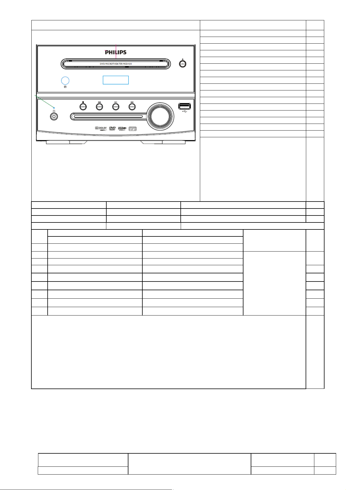
MCD130 – DVD Micro Theatre
Hardware Requirement Specification
Valid for stroke version:
Stroke
Version
/12
/05
/37 USA & Canada
/51 Russia
/55 Latin America (Including Mexico)
/93
/94 India
/96
/98
Europe
UK
China
Taiwan
Asia Pacific (except Korea, Thailand)
Countries / Region MCD130
√
√
√
© Philips Electronics N.V. 2012
This information is furnished for guidance, and with no guarantee as to its accuracy or completeness; its publication conveys no license under
any patent or other right, nor does the publisher assume liability, for any consequence of its use; specifications and availability of goods
mentioned in it are subject to change without notice; it is not to be reproduced, in whole or in part, without the written consent of the publisher.
MCD130
Page 1 of 10
PRODUCT SPEC
Sheet-190
Rev.1.0
Page 6

MCD130 DVD Micro Theatre
Technical Specifications (Philips Sheet-190)
Contents
1. EPICTION...................................................................................................................................................3
2. ACCESSORIES.............................................................................................................................................3
3. GeneralDescription..................................................................................................................................4
4. Safetyrequirements..................................................................................................................................5
5. BSMIrequirements...................................................................................................................................5
6. CCCrequirements.....................................................................................................................................5
7. Power‐Supply............................................................................................................................................5
8. Audio(alltestwith22kOhmloadunlessspecified).................................................................................6
9. Speaker(alltestwith8Ohmdummyload)...............................................................................................6
10. VideoOutput.............................................................................................................................................6
11. YUVVideoOutput.....................................................................................................................................7
12. MiscellaneousElectrical............................................................................................................................7
13. PlayabilityRequirement(Seeattachedinlastpage)................................................................................8
DISCPlayability(detailsrefertoPlayabilityTestPlan).........................................................................................8
PowerOn/OffDisturbances...................................................................................................................................9
14. MechanicalSpecification(ReferPQRorPQP).........................................................................................10
15. Criticalcomponent..................................................................................................................................10
16. CosmeticSpecification............................................................................................................................10
17. ChangeHistory........................................................................................................................................10
Acceptance Status Version: 1
Department Development PS & P Project Representative
Name Gavin He & Waley Chen Keith CHOW Simon Wong
Date
Sign
MCD130
Page 2 of 10
PRODUCT SPEC
Sheet-190
Rev.1.0
Page 7
1. EPICTION
DESCRIPTION Pos
DVD door
Open /Close button
Remote IR Sensor
Power and play indicator
Power button
Stop button
Previous button
Play/Pause button
Next button
Vol button
USB Jack
CABINET
Dimensions (L x W x H): TBA Material: Refer to Cosmetic Specification
Finishing: Refer to MUS specification
Bear unit weight (kg) TBA
Main set
CVBS &YUV OUTPUT X 1 RCA4 x1
L/R OUTPUT X 1 RCA 2x1
Speaker connector 2 red + 2 black
2. ACCESSORIES
1) Warranty Card
2) Remote Control,
3) User Manual,
4) Video cord 1.2m
5) Speaker wire(one side fixed in speaker)
Connector type
MCD130
Page 3 of 10
PRODUCT SPEC
Sheet-190
Rev.1.0
Page 8
3. General Description
DVD Micro Theatre
Key Components:
Optical Pickup: S76RFXP2 (IM)
Chip set/Solution: MT1389QEHN-W
Disc Size: 8cm/12cm
Playable disc type: DVD/DVD+RW/DVD+R/CD/CD-R/CD-RW / DVD-R/-RW
Video output signal: PAL/AUTO/NTSC (output only, with Macrovision)
Video format: DVD / VCD / SVCD / JPEG /
Audio format: CD/MP3, MP3-DVD, Dobly digital (down mix), WMA
User Interface:
OSD language:
English,Trad-Chinese, Beharsa Melayu. Thai, Korean for 98 version
Eng, Simplified-Chinese for 93version
Eng, Trad-Chinese, for 96 version
(Detail, refer to UI requirement)
Screen Saver function.
Button functions: Refer to MUS.
Standby power: <1.0W
Picture Quality: refer to DVP3600/98 (NO VIDEO BUFFER)
Sound Quality: refer to MCD2010 (NO OUTSIDE 2CH AUDIO DA)
USB Performance: refer to DVP3600/93 without CD Ripping function
Lifetime : 3 years (min.)
Temperature & Humidity:
Operating Temperature & Humidity
0-50 deg C / 30-90%; Charging Temperature: 0 - +40 degC
Storage Temperature & Humidity
-20-70 deg C / 30-95%
Climatic requirements, Indoor product
Weight:
TBC Kg +/- 30% with / Video cord / IFU / GB
Version Region Countries Voltage Frequency ACCordType
93 6 China 110V‐240V 50Hz,60Hz CCCflat2‐pin
96 3 Taiwan 110V‐240V 50Hz,60Hz TaiwanPlug(CNS690approved)
98 3 Asia 110V‐240V 50Hz,60Hz VDE2‐pinsround
MCD130
Page 4 of 10
PRODUCT SPEC
Sheet-190
Rev.1.0
Page 9
4. Safety requirements
CB approval
MCD130
IEC60065:2001 + A1:2005 & EN60065:2002 + A1:2006,
5. BSMI requirements
– Active Radiation, Radiation Immunity, Conductive Interference
CNS 13438/CNS 13439
6. CCC requirements
GB8898-2001 / GB13837-2003 / GB17625.1-2003
7. Power-Supply
AC Power
Power Supply voltage 100- 240V +/- 10%
Standby Power (power switch OFF) - <1W
Typical
Limit
Remarks
MCD130
Page 5 of 10
PRODUCT SPEC
Sheet-190
Rev.1.0
Page 10
8. Audio (all test with 22k Ohm load unless specified)
)
DVD-Audio Line out
1. Output voltage
1kHz (V)
Condition Typical
2Vrms +/- 1dB
Limit
Apply 8 ohm loading no component
damage
2. THD 20-20kHz 0.03%
3. Dynamic range 1kHz >85dB
4. A-weighted S/N ratio Tr15/Tr49 >90dB
5. Frequency response 20-20kHz - +1 / -0.5dB
6. Channel separation 1kHz - >=85dB
7. Channel balance 1kHz +/- 1dB
0.06%
9. Speaker (all test with 8 Ohm dummy load
CDDA-Speaker Out
1. Output power RMS
1kHz
2. Max THD 1kHz Volume max 20%
3. THD Test Power: 1w
Reference: 1kHz
4. Frequency response
5. S/N ratio
6. Max Hum noise CDDA 1kHz/0dB; Vol=Max - <2mV
7. Min Hum noise CDDA 1kHz/0dB; Vol=1 - <2mV
8. Channel separation 1kHz - >=30dB
9. Channel balance
DVD Dolby 1.5
0dB
Test Power: 1w
Filter: A-weighted
Test power: 1w
Condition Typical
CDDA 1kHz/0dB
THD 10%
100Hz -
1kHz -
10kHz -
40Hz -3dB
100Hz 10dB
1kHz 0dB Ref
10kHz 0dB
20kHz -3dB
1kHz - >67dBA
5kHz - >67dBA
1kHz 0dB +/- 2dB
10W >10W
Limit
>20%
<1%
<1%
<1%
+/-2dB
+/-2dB
+/-2dB
+/-2dB
10. Video Output
AV output ports special requirement
Connection Port Impedance
>10V DC
75 ohm
No component damaged
MCD130
Page 6 of 10
PRODUCT SPEC
Sheet-190
Rev.1.0
Page 11
CVBS Video Output (PAL / NTSC)
DVD-Video composite
1. White Bar - 714mVpp +10/-20
2. Sync. Amplitude - 286mVpp +/-40
3. Amplitude o/p - 1000mVpp +10/-20
4. Burst amplitude - 286mVpp +1/-4
5. Burst/chroma ratio - - +/-10
6. S/N luminance Un-weighted - >55
7. S/N chroma (AM) Un-weighted - >55
8. S/N chroma (PM) Un-weighted - >52
9. Video bandwidth - PAL/8MHz -7
10 Chroma/Luminance <100
11 Sub-carrier
frequency (Chroma)
(ppm)
Condition Typical Limit
- 4.43361875MHz / PAL
3.579545MHz / NTSC
+/-30
12 Subcarrier locked /
unlocked
- - Locked
11. YUV Video Output
Description Test Signal Specification Class achievement
NTSC PAL NTSC PAL
Y White level
Sync.amplitude
U amplitude o/p
V amplitude o/p
S/N on outputs: U
V
Video Bandwidth (0.5MHz10MHz)
multi-burst ( T2
C9 )
View test: For both NTSC and PAL a viewing test is necessary to determine any annoying phenomena which
can not be determined by standard video measuring procedures. In case of the doubt, the viewing test is
decisive
100% White 714 mVpp
+/- 10%
100% White
75% color bar
( T2 C1 )
75% Colour bar 525mV ±
100% red
( T2 C17 )
Multi-burst +1dB/-6dB +1dB/-6dB
video amplitude
0.5MHz
1.0MHz
2.0MHz
4.0MHz
4.8MHz
5.8MHz
286 mVpp
+/- 40mV
286mV ±
40mV
10%
≥55 dB*
Ref. 0dB
90.8 IRE
+1dB / -
1dB +1dB / -1dB
+1dB / -
1dB +1dB / -1dB
+1dB / -
2dB +1dB / -2dB
+1dB / -
3dB +1dB / -3dB
+1dB / -
5dB +1dB / -5dB
+1dB / -
10dB +1dB / -10dB
700 mVpp +/-
10%
300 mVpp
+30mV / -
50mV
300mV ±
50mV
525mV ± 10%
≥55 dB
12. Miscellaneous Electrical
1. EMC for EURO EMC - 4dB Below Limit
2. ESD test(UAN-D1724) <= 8kV - Ok No abnormal allowed
<= 15KV - Ok No component damage
3. Mains spike +/-1500V - Ok
4. Mains failure 100% mains drop - Ok Refer to CTQ
MCD130
Page 7 of 10
PRODUCT SPEC
Sheet-190
Rev.1.0
Page 12
5
2
. Laser beam shut off
when the CD door open
- - Ok
Auto Power Off
Con Typical Limit
Screen saver - 15 +/-30%
Power off –stand by - 20 +/-30%-
IR remote
Max. operating
(degree)
Quiescent Current
Operating Voltage
Operating Current
Carrier Frequency
Battery Storage Time
Battery Life Time After 20 hours continuous sending (2s/time), IR power should be at least 20µW/cm
Condition Typical Limit
<= +/- 45
<= +/- 30
。
。
。
0
- 5
- 7
- 10
- <1uA
2.3 - 3.5V
9 – 16mA
36KHz +/- 2%
? Year
After push / disc stop
After Screen saver functional
(M)
(M)
(M)
Temperature:
Audio/ Video Characteristic Testing discs
Manufacturer Disc name
1) TOSHIBA
TSD-4
2) DOLBY Test disc
3) ABEX TDV-540A
4) SONY Test CD Type 4
13. Playability Requirement (See attached in last page).
DISC Playability (details refer to Playability Test Plan)
DVD Video playability
1. Scratch
MCD130
Page 8 of 10
Condition Typical Limit
-
- <=1.6
PRODUCT SPEC
Sheet-190
ABEX TDV-541
Rev.1.0
Page 13

2. Black dot
3. Fingerprint
4. Non-Centre
5. Vertical deviation disc
DVD+ RW Video playability
Normal playback
Black dot
Fingerprint
Condition Typical Limit
-
-
-
-
- NA
- NA
- NA
- NA
OK
0.8
OK
ABEX TDV-545
ABEX TDV-545
ABEX TDV-552
ABEX TDV-562
Philips HAC11
Philips HAC11
Philips HAC11
Philips marginal DVD-9
CD playability
Abex-TCD732RA(VDD) Track 15
Abex-TCD713(ECC 210um)
Condition Typical Limit
OK
OK
NA
Philips LVP12.01 – layer 0
Philips LVP12.02 – Layer 1
Power On / Off Disturbances
> -52 dB suppression of the disturbance with regard to the rated output voltage.
The peak level has to be measured according to IEC 60651 weighted (A) curve.
MCD130
Page 9 of 10
PRODUCT SPEC
Sheet-190
Rev.1.0
Page 14

14. Mechanical Specification (Refer PQR or PQP)
15. Critical component
Description Manufacturer Model no. Version
DVD Chip set MTK MT1389QEHN-W
Laser pick up IM S76RFXP2
Remote Control
Power IC Infineon 0B2273AMP(SOT23-6)
LOADER KeQin RT-628
FLASH(16M)
IC(AMP)
TianZeHuan
EON/MX EN25QH16-104HIP/MX25L1606EM2I-12G
TI TPA3110D2
T47
16. Cosmetic Specification
All cosmetic color please refer Philips MUS color specification
No. Part Description Texture
Finishing Color Remarks
17. Change History
Version Date Description by
0.1 2011-11-09
initial Eric
MCD130
Page 10 of 10
PRODUCT SPEC
Sheet-190
Rev.1.0
Page 15

2
How to remove the CD manually from the tray
1. Please do as below instruction in ca
a. Power off the DVD player.
b. Please gently push the guider and wait until the tray comes out(Figure1).
se the tray can not be open:
use ji
g move this part left
Page 16

How to open the set
Step Items Pics Remark
6pcs 3*6PWB Screw
1
Topcover
Total 12 PCS Screws
6 Pcs 3*6PWB Screw
4Pcs 3*8BT Screw(White)
4Pcs 3*8BT Screw(White)
2
Loader
Each side 1pcs 3*6FB Screw
Each side 1pcs 3*6FB Screw
Open power cord jack
Open power cord jack
Total 4 PCS Screws
3
Rear panel
2Pcs3*8PB Screw
2Pcs3*8PB Screw
2 Pcs 3*6PWB Screw
2 Pcs 3*6PWB Screw
2 pcs 3*6PWB screw
2 pcs 3*6PWB screw
Total 8 pcs Screw
Page 17

4
Loader holder
Each side 2 pcs 3*6FB
Screw
Total 4 PCS Screw
5
6
7
PCBA
Front Panel1
Front Panel2
2Pcs 3*6PWB Screw
2Pcs 3*6PWM Screw
2Pcs 3*6PWM Screw
Front Panel
Total 2 PCS Screw
Total 2 PCS Screw
Total 6 PCS Screw
6 pcs 3*8PA Screw
Page 18

3
C
NG
How to check the return unit
1,No Vid
output
No Vi
deo output
eo
Connect the
Insert the AC Power line into
the connectors
Press the standb
power on the set
The display on the set
The “Philips” logo should be
on the screen and the witch
will display
AV OK
y button to
OK
The “Philips”
NG
NG
Insert the AC power
line over again
be on the screen and the
witch will display
module Fail
logo should
OK
The LED
Replace
NG
TEST 1.2V and 3.3V
OK
Replace Q5,Q6
Replace flash U1
NG
The DSP
Fail
1
Mainboard PCBA
Power
PSU Fail
Replace
frontboard
BA
P
Page 19

2, No Audio output
No Audio output
Connect the AV OK
Power on the set
4
Play the disc and the audio will
output from the TV
OK
Test Finish
NG
Adjust the volume +
to add the volume
from the TV
NG
The Audio DA Fail
or the DSP Fail
Replace
Mainboard PCBA
Page 20

3, No playing any discs
g
aga
No playing any discs
Connect the AV OK
Power on the set
Open the tray door and
put into the DVD or CD
disc to closing the tray
door
5
The servo chip or
DSP chip fail
The system will loading
the disc, and on the
screen display the
‘Loading’ OSD
The disc’s info will
display the screen
NG
Note to hear the
playback sound when
close the tray door to
playing the disc
NG
NG
Please power off, then
power on the set to
playback the disc over
in
Replace
Mainboard PCBA
NG
Replace LOADER and
check a
The loader or servo
chip or DSP chip fail
ain
NG
Page 21

6
Software upgrade
1. Get the software firmware,the name must be MCD130/XX.BIN, and all character must be
large.
or press SETUP key on the RC,in “ Preferences” menu can see the option of “Version info”,
Then, enter the Version info menu and you can see its upgrade file which shown of File
Name
2. Copy the upgrade firmware onto CD disc.
3. Play the firmware CD disc,and the upgrade menu will appear.
4. First Select PLAY button and start to automatically upgrade on the first upgrade menu.
5. Then,the upgrade process will start and appear “Upgrading”,please don’t power off during this
state.
6. During the updating, the tray door is openning,. when the update is complted, the unit will power off and
then re-start
automatically to close the tray door to play the current disc on the tray.
Upgrade file detected
Upgrade ?
press PLAY to start
Upgrade file detected
Do not power off
Upgrading
Page 22

7
How to select the right language
(1) How to change the OSD language
First, press SETUP key on the RC,in “ Gereral Setup” you can see the option of “OSD
Language”,
Then,press Right key to enter the osd language menu and select language which you want.
(2) How to change the Audio default language
First, press SETUP key on the RC,in “ Preferences” menu can see the option of “Audio”,
Then,press Right key to select Audio or subtitle language. which you want
Page 23

5
9-1
4
3
2
1
BLOCK DIAGRAM
VOLUME CONTROL
WP1
FLASH
U102
L/R
OPA
PT2257
VOLUME CON
CLASS D
TDA3110
L/R
AMPLIFLER
CONNECTER
D D
CD/DVD
C C
OPU
HD850
/WTP-AD01
SDRAM
1MX16/4MX16
U100
MT1389W
L/R
AUDIO R/L LINE OUT
Y,U,V/CVBS
JK104
YUV/CVBS OUTPUT
R/L AUDIO OUTPUT
+5V
ADJ_33
ADJ_12
MOTOR DRIVER
J1(16PIN/1.0)
CONNECTOR
USB INPUT
TO FRONT BOARD
+P12V(to 4558 and mute)
PWCTRL1
B B
PWCTRL3
USB_5V(to USB)
AVCC(to OPU)
STB_5V
AC IN
100-240V
PWM POWER
OB2273A
PU1
PT1
ZY-T00113
+13V
DC TO DC
AP2953
PWCTRL2
3.3V(to MT1389W)
ADJ_33
1.2V(to MT1389W)
A A
TO CLASS D
ADJ_12
TO FRONT BOARD
NOTE: THE POWE SUPPLY PART
TO MOTO DRIVER
5
4
3
2
1
Page 24

5
9-2
4
3
2
1
SET WIRING DIAGRAM
D D
SPEAKER L
SPEAKER R
PB/UP
Y/DOWN
PR/UP
L-CH/UP
CVBS/DOWN
R-CH/DOWN
16P FFC WIRE
TO FRONT BOARD
CF4558
C C
TPA3110D2
MT1389QEHN-W
MX25L1606E
USB-5V
USB-DM
USB-DP
GND
TO USB
24P FFC WIRE
1.2V ADJ
AP2953
3.3V ADJ
TO LOADER OPU
TRIN
GND
TROUT
LOAD+
LOAD-
SP-A
SP+
TROUT
GND
SL-
SL+
TO LOADER
B B
A A
AC IN
FUSE
5
4
3
2
1
Page 25

5
9-3
4
3
2
1
CIRCUIT DIAGRAM - MAIN BOARD
PART 1
PD9
PD9
TO220-3P
PT1 EFD25
PT1 EFD25
D D
C C
B B
PD1
PD1
PD4
PD4
RL207
RL207
RL207
RL207
CAP-10X14X7-CT7Y333
CAP-10X14X7-CT7Y333
PR222
PR222
1M/1206
1M/1206
PR224
PR224
1M/1206
1M/1206
PRT1
PRT1
5D207
5D207
PCON1
PCON1
UF16-40mH
UF16-40mH
PCX1
PCX1
0.22u/250VAC
0.22u/250VAC
2 3
PLF2
PLF2
1 4
1mH
1mH
PRV1
PRV1
10D471
10D471
CAP-10X14X7-CT7Y333
CAP-10X14X7-CT7Y333
1
L
23
PLF1
14
PR223
PR223
1M/1206
1M/1206
PR225
PR225
1M/1206
1M/1206
PF1
PF1
T2A
T2A
PD2
PD2
PD5
PD5
RL207
RL207
RL207
RL207
PR218
PR218
470K/1206
470K/1206
NC/24K-1206
NC/24K-1206
PC11
PC11
PR219
PR219
470k/1206
470k/1206
PR226
PR226
102/25V/0805
102/25V/0805
PR220
PR220
470k/1206
470k/1206PLF1
PU1
PU1
3
2
OB2273A
OB2273A
PEC1
PEC1
+
+
150uF/400V
150uF/400V
RI
FB
0.1uF-50V-K-0805(X7R)
0.1uF-50V-K-0805(X7R)
PD7
PD7
FLZ18VC
FLZ18VC
5
VDD
6
GATE
4
CS
GND
1
PC8
PC8
68K/2W
68K/2W
10R/1206
10R/1206
PC9
PC9
+
+
47uF/50V
47uF/50V
PR227
PR227
100R/0603
100R/0603
PR229
PR229
1K/0805
1K/0805
PC12 101-0805PC12 101-0805
PR215
PR215
PR221
PR221
PD6
PD6
FR107
FR107
PD8
PD8
3906
3906
PQ2
PQ2
PR23122R-0805PR23122R-0805
PR232470R/1206PR232470R/1206
PC2
PC2
472/1KV
472/1KV
HER207
HER207
PQ1
PQ1
10N60
10N60
3
PR230
PR230
10K/0805
10K/0805
PR235 1R-1206PR235 1R-1206
PR236 2R2-1206PR236 2R2-1206
PR237 2R2-1206PR237 2R2-1206
PR238 2R2-1206PR238 2R2-1206
10
10
NP1
NP1
11
NC
NP2
NP2
12
12
8
8
NP2
NP2
9
9
40R
40R
PFB1
PFB1
2
PC10
PC10
101/1KV
101/1KV
1
43
PU2
PU2
PC817
PC817
PU3
PU3
TL431
TL431
PCY3
PCY3
222
222
PR2391KPR239
1K
PR228
PR228
470R-0805
470R-0805
12
NC
12V
12V
NB2
NB2
GND
GND
NB1
NB1
5V
5V
PR2331KPR233
1K
PR240
PR240
36K
36K
1
6
7
4
5
2
3
+12V
此处元件由
PR21722R/1206PR21722R/1206
TO220-3P
SBR20100
SBR20100
1
1
3
3
PR21622R/1206PR21622R/1206
PR234
PR234
36K
36K
PC13
PC13
2.2u-0805
2.2u-0805
PC14
PC14
0.1uF(X7R)
0.1uF(X7R)
PR241
PR241
10K
10K
0402改0603
2
PC4
PC4
680PF
680PF
PC7
PC7
680PF
680PF
+12V
PL1
2
PC5
PC5
+
+
1000uF/25V
1000uF/25V
PL1
10uH/3.8A
10uH/3.8A
PC6
PC6
+
+
1000uF/25V
1000uF/25V
PC3
PC3
470uF/16V
470uF/16V
+
+
+12V
PC1
PC1
0.1uF-0603
0.1uF-0603
2
N
2Pin-7.92mm
2Pin-7.92mm
CON2X1X7.9-VS
CON2X1X7.9-VS
PD_CTRL:
1: ON,
0: OFF
+12V
PL3
PL3
FB600R
FB600R
LC1206
LC1206
ECAP-2.5X6.3
ECAP-2.5X6.3
A A
5
PC17
PC17
220uF16V
220uF16V
+
+
CC0402
CC0402
4
100nF
100nF
PC18
PC18
PC19
PC19
10uF
10uF
CC1206
CC1206
PR243
PR243
RC0402
RC0402
10K
10K
CORE VOLTAGE
PC15 10nF
PC15 10nF
CC0402
PU4
PU4
1
BS
2
IN
7
EN
AP2953
AP2953
SO8X1.27-4.9X3.9-E
SO8X1.27-4.9X3.9-E
CC0402
CC0402
CC0402
MP1482 2A 340KHZ
MP1482 2A 340KHZ
VFB = 0.923V
VFB = 0.923V
VIN :4.75V ~ 18V
VIN :4.75V ~ 18V
SS
8
PC22
PC22
NC
NC
4
GND
SW
COMP
ON IN STANDBY MODE, OFF IN PM MODE
PL2
PL2
10uH/3.8A
10uH/3.8A
LC-10X9X5-S
LC-10X9X5-S
24K
PR242 150K1%
PR242 150K1%
CC0402
CC0402
20K
PR245
PR245
33K1%
33K1%
RC0402
RC0402
RC0402
RC0402
PC1622PF/NC
PC1622PF/NC
100nF
100nF
CC0402
CC0402
FB
3
5
CC0402
CC0402
PC20
PC20
6
5.6nF
5.6nF
PR244
PR244
2K2
2K2
RC0402
RC0402
3
PC21
PC21
STB_5V
PEC2
PEC2
+
+
470uF16V
470uF16V
ECAP-5X8
ECAP-5X8
2
1
Page 26

5
9-4
4
3
2
1
CIRCUIT DIAGRAM - MAIN BOARD
PART 2
DV33
PR214
Serial Flash
D D
12
R176
R176
10KΩ
10KΩ
SF_1
SF_3
C C
U102
U102
1
/CS
2
DO
3
/WP
4
VSS
EN25F16
EN25F16
8 PIN SOIC Package
4 5
3
2
1
VCC
/HOLD
CLK
208Miles
TF1
TF1
DIO
8
7
6
5
6
7
8
SF_7 SF_DISF_2
27Ω
27Ω
R175
R175
10KΩ
10KΩ
C127
C127
NC
NC
GND
PR214
12
1 2
SF_5
SF_6
C126
C126
0.1uF/25V
0.1uF/25V
SF_1
SF_2
DV33
8642
8642
33Ω*4
33Ω*4
RN1
RN1
7531
7531
SF_CS
SF_DO
SF_CK
OFF-PAGE CONNECTION
SF_CS
SF_DO
SF_DI
SF_CK
FLASH I/F
USB_DM
USB_DP
USB I/F
DV33
POWER
SF_CS [2]
SF_DO [2]
SF_DI [2]
SF_CK [2]
USB_DM [2]
USB_DP [2]
DV33
FLASH auto test
FLASH auto test
FLTP
FLTP
R177 10KΩ
R177 10KΩ
RC0402
RC0402
SF_CS
VOLUME CONTROLLER
B B
LCH RCH
AUDIO_L
SDA_PT
SCL_PT
A A
LCH RCH
SDA_PT
SCL_PT
C172 10uFC172 10uF
C174 10uFC174 10uF
R223 100RR223 100R
R225 100RR225 100R
R221
R221
0R/NC
0R/NC
C176
C176
27pF
27pF
1
LIN
2
LOUT
3
VSS
4
SDA
PT2257/2259
PT2257/2259
U103
U103
RIN
ROUT
VDD
SCL
R222
R222
0R/NC
0R/NC
8
7
6
5
C173 10uFC173 10uF
C175 10uFC175 10uF
EC123
EC123
+
+
100uF/16V
100uF/16V
C177
C177
27pF
27pF
AUDIO_RAUDIO_L
BC1
BC1
0.1uF
0.1uF
AUDIO_R
R226
R226
2.2K
2.2K
L119
L119
R224
R224
430R
430R
4.7R/NC
4.7R/NC
AVCC
+P12V [3]
5
4
3
2
1
Page 27

5
9-5
4
3
2
1
CIRCUIT DIAGRAM - MAIN BOARD
PART 3
R147
R147
59KΩ
D D
59KΩ
C113 68PF/50VC113 68PF/50V
+P12V
R151
EC114
EC114
AL
10uF/25V
10uF/25V
C C
EC116
EC116
+
10uF/25V
10uF/25V
+
AR
R2020ΩR202
+
+
12
0Ω
R2010ΩR201
12
0Ω
C144NCC144
NC
R150
R150
10KΩ
10KΩ
C145NCC145
NC
R156
R156
10KΩ
10KΩ
R151
5.1KΩ
5.1KΩ
OP_Vref
C114
C114
1000PF/25V
1000PF/25V
R155
R155
59KΩ
59KΩ
R157
R157
5.1KΩ
5.1KΩ
OP_Vref
C120
C120
1000PF/25V
1000PF/25V
2
3
C119
C119
6
5
-
-
+
+
8 4
-
-
+
+
8 4
U101A
U101A
NJM4558
NJM4558
+12VA
68PF/50V
68PF/50V
U101B
U101B
NJM4558
NJM4558
+12VA
EC115
EC115
+
+
1
1 2
10uF/25V
10uF/25V
A_MUTE
R152
R152
1KΩ
1KΩ
R154
R154
330Ω
330Ω
LCH#
R153
R153
100KΩ
100KΩ
CE1
Q110
1
Q110
2N3904
2N3904
SOT23
SOT23
2 3
CE1
220uF/16V
220uF/16V
Audio OP
EC117
EC117
+
7
+
1 2
10uF/25V
10uF/25V
A_MUTE
R158
R158
1KΩ
1KΩ
R160
R160
330Ω
330Ω
RCH#
R159
R159
100KΩ
Q111
1
Q111
2N3904
2N3904
2 3
100KΩ
chang to 220R
R146
R146
220Ω
220Ω
+12VA OP_Vref
12
+
+
ECAP-2.5X6.3
ECAP-2.5X6.3
+12VA
C115
C115
0.1uF/25V
0.1uF/25V
R148
R148
30KΩ
30KΩ
C116
C116
0.1uF/25V
0.1uF/25V
R149
R149
30KΩ
30KΩ
OP_Vref
12
+
+
EC113
EC113
100uF/10V
100uF/10V
ECAP-2.5X5
ECAP-2.5X5
AudioMute
DV33
AR
B B
R167
D110
D110
BAV99
BAV99
SOT23
SOT23
R173
R173
47KΩ
47KΩ
R167
R169
R169
0/NC
0/NC
1KΩ
1KΩ
2
1
1
1
23
Q115
Q115
2N3906
2N3906
GPO14:
Mute: H
UnMute: L
AUDIO_MUTE
+P12V
3
R171
R171
100KΩ
100KΩ
A A
12
EC120
EC120
+
+
47uF/16v
47uF/16v
R164
R164
10KΩ
10KΩ
R168 1KΩ
R168 1KΩ
Q114
Q114
2N3904
2N3904
2 3
EC119
EC119
+
+
220uF/16V
220uF/16V
RC0402
RC0402
1
R163
R163
100Ω
100Ω
23
Q113
Q113
2N3906
2N3906
R170
R170
100Ω
100Ω
A_MUTE
AL
A_MUTE
AUDIO_MUTE
RCH#
LCH#
AUDIO I/F
+P12V
DV33
AR [2]
AL [2]
A_MUTE [2]
AUDIO_MUTE [2]
RCH [5]
LCH [5]
+P12V [1]
DV33 [1,2,3,6]
Power
5
4
3
2
1
Page 28

5
9-6
CIRCUIT DIAGRAM - MAIN BOARD
PART 4
4
3
2
1
CN101
C101 0.1uFC101 0.1uF
89W_3V3
R117 10kR117 10k
D D
89W_3V3
R120 10kR120 10k
SLSL+
GPI36 TROUTLIMIT
F-
1
F+
2
T+
3
T-
4
C/c
5
D/d
6
CD/DVD SW
7
RF
8
A/a
9
B/b
10
F
11
GND-PD
12
Vc(Vref)
13
Vcc
14
E
15
NC
16
VR-CD
17
VR-DVD
18
CD-LD
19
MD
20
HFM
C C
B B
A A
21
NC
22
DVD-LD
23
GND-LD
24
SANYO HD6x
25
26
1
2
3
4
5
6
7
8
9
10
11
12
13
TOP
TOP
14
15
16
17
18
19
20
21
22
23
24
24pin-0.5mm
24pin-0.5mm
CN100
CN100
J1J1
1
2
3
4
5
6
7
8
9
10
11
12
13
14
15
16
4P/2.0J24P/2.0
4
3
2
1
J2
PLAY_LED_CON
LOADLOAD+
TROUT
TRIN
SPSP+
LIMIT
LD-DVD
AVCC1
LD-CD
VR_DVD
VR_CD
E
AVCC1
V20
CB117 0.1uFCB117 0.1uF
F
B
A
RFO
IOA
D
C
T-
T+
F+
F-
R144
R144
IR_IN#
PLAY/PAUSE_KEY#
STB+5V#
STB_KEY#
STB_KEY
OP/CL_KEY#
CB134
CB134
0.1uF/25V
0.1uF/25V
MLVG0603100NV05BP/NC
MLVG0603100NV05BP/NC
CN101
1
2
3
4
5
5pin/2.0
5pin/2.0
6pin/2.0
6pin/2.0
6
5
4
3
2
1
CN102
CN102
C117
C117
0.1uF
0.1uF
VFD
VSCKUP1_6
VSDAUP1_7
VSTBGPIO13
10Ω
10Ω
STB_LED_CONTROL#
CB126100PF/50V CB126100PF/50V
CB127
CB127
CB128
CB128
CB129
CB129
100PF/50V
100PF/50V
100PF/50V
100PF/50V
FB120R
FB120R
C24
C24
C25
C25
R178
R178
100PF
100PF
5.1Ω
5.1Ω
12
12
USB_5V
R179
R179
5.1Ω
5.1Ω
12
ED100
ED100
LC0603
LC0603
L101
L101
FB
FB
EC106
EC106
+
+
C111
C111
100uF/10v
100uF/10v
0.1uF
0.1uF
ECAP-2.5X5
ECAP-2.5X5
TO FRONT BOARD
CB1
CB1
100PF/50V
100PF/50V
FB1 600Ω/150mAFB1 600Ω/150mA
CB130
CB130
CB131
CB131
GND
100PF/50V
100PF/50V
100PF/50V
100PF/50V
100PF
100PF
SERVO RF DeCAP.
89W_1V2
89W_1V2
R121 0R121 0
AVCC
89W_3V3
STB_5V
R8
4.7KΩR84.7KΩ
L105 600Ω/150mAL105 600Ω/150mA
L107 600Ω/150mAL107 600Ω/150mA
L106 600Ω/150mAL106 600Ω/150mA
FB103 600Ω/150mAFB103 600Ω/150mA
FB124 600Ω/150mAFB124 600Ω/150mA
FB100 600Ω/150mAFB100 600Ω/150mA
100PF/50V
100PF/50V
L21
L21
L22FB120R L22FB120R
1N4148(SMT)
1N4148(SMT)
USB_DP
USB_DM
USB_DM
ED101
ED101
MLVG0603100NV05BP/NC
MLVG0603100NV05BP/NC
EC112
EC112
12
10uF/10V
10uF/10V
GND
21
D5
D5
D6
D6
1N4148(SMT)
1N4148(SMT)
USB_5V
close to USB connector
CB108
CB108
0.1uF
0.1uF
CB111
CB111
0.1uF
0.1uF
89W_3V3
R123 0R123 0
CB114
CB114
0.47uF
0.47uF
R129 0R129 0
R203 8.2RR203 8.2R
L102 120Ω/500mAL102 120Ω/500mA
R140
R140
4.7KΩ
4.7KΩ
1 2
1 2
FB102 600Ω/150mAFB102 600Ω/150mA
R9
nc/4.7KR9nc/4.7K
1 2
1 2
STB_5V
21
R37
R37
4.7K
4.7K
AVCC
R
B
G
FS
Crystal
81
80
79
78
77
76
75
74
73
72
71
70
69
68
67
66
65
64
63
62
61
60
59
LED_PLAY CONTROL
58
57
56
55
R115 100kR115 100k
C105
C105
27pF
27pF
Put these circuits as closer
as possible to MT1389W
V_R
V_B
V_G
DACVDD3
CVBS_OUT
DACVDD3
GPIO14
ADC_KEY1
ADC_KEY2
GPIO20
GPIO32
SCL_PT
SDA_PT
GPIO29
GPIO7
GPIO8
GPIO3
R128 560R1%R128 560R1%
RC0402
RC0402
R13 4.7K
R13 4.7K
R14
R14
GPIO6 TxD
GPIO11 RxD
TP8TP8
TP9TP9
TP13TP13
TP6TP6
R138
R138
4.7k
4.7k
4.7K
4.7K
DV33
C104
C104
27pF
27pF
CB119
CB119
0.1uF
0.1uF
CB116
CB116
0.1uF
0.1uF
89W_3V3
Download RS-232
RC0603
C107 0.1uFC107 0.1uF
AVDD12_AUDIG
94
95
AVDD12_1
AVDD12_AUDIG
47
SF_DO
SF_CS
R116 4R7
R116 4R7
10uF/10v
10uF/10v
C103
C103
+
+
220uF/10v
220uF/10v
ECAP-2.5X6.3
ECAP-2.5X6.3
EC100
EC100
TP15TP15
AL
ADACVDD
92
93
91
ALS / GPIO
ADACVDD1
ADACVDD2
ALF / CENTER / GPIO
UP1_7
UP1_6
SF_CK
SF_DI
RC0603
R119 0R119 0
C109 10uF/10vC109 10uF/10v
AR
AVCM
90
89
AVCM
AL / GPIO1
IR
GPIO13
89W_1V2
CB120
CB120
0.1uF
0.1uF
89W_3V3
RFV12-1 XIXIXIXI XO
RFV12-2
AVDD12_AUDIG
CB112
CB112
0.1uF
0.1uF
CB113
CB113
0.1uF
C110
C110
4.7uF
4.7uF
CB115
CB115
0.1uF
0.1uF TP10TP10
EC109
EC109
+
+
100uF/10v
100uF/10v
R141
R141
4.7KΩ
4.7KΩ
1 2
R145
R145
nc/4.7K
nc/4.7K
VOL+
VOL-
R36
R36
4.7K
4.7K
0.1uF
3V3_FB
MD_VCC
LD-CD
EC107
EC107
+
+
47uF/6.3v
47uF/6.3v
MD_VCC
CB118
CB118
0.1uF
0.1uF
STB_5V
R142
R142
R143
R143
4.7KΩ
4.7KΩ
4.7KΩ
4.7KΩ
1 2
1 2
LED_PLAY CONTROL
IR
VSCK
VSTB
GPIO32
VSDA
GPIO29
LD-DVD
CB142
CB142
0.1uF
0.1uF
R118 0R118 0 Y100 27MHzY100 27MHz
89W_3V3
R122
R122
4R7
4R7
RC0603
RC0603
XI
R124 51R124 51
XO
R125 51R125 51
AVDD33
V20
VR_CD
R126 0R126 0
VR_DVD
R127 0R127 0
L113
10uH
10uH
RESET_C
ADJ_33
MD_VCC
L114
LC0805L114
LC0805
10uH
10uH
LOADLOAD+
V1P4
TT+
FF+
LD_IN
SL+
SLSP+
SP-
R132 0R
R132 0R
RC0603
RC0603
STB_5V
RFVDD3 V1P4V1P4
C100
C100
C102
C102
4.7uF
4.7uF
0.1uF
0.1uF
AADVDD
C106
C106
6800pF
6800pF
EC105
EC105
+
+
100uF/10v
100uF/10v
U100
U100
1
PAD_XTALI
2
PAD_XTALO
3
AVDD33_2_1
4
PAD_V20
5
6
7
8
9
10
11
12
13
14
15
16
17
18
19
20
21
22
23
24
25
26
27
89W_3V3
CB121
CB121
0.1uF
0.1uF
89W_3V3
PAD_VR_CD
PAD_VR_DVD
LD_D
RESET_C
V33
TRB1
MOROR_VCC1
LD_C
VOTRVOTR+
LD_VCC
V14/VBIAS
VOTK+
VOTKVOFCVOFC+
LD_IN
VOSL+
VOSLVOLD+
VOLDMOTOR_VCC2B
MOTOR_VCC2A
GND
28
ADJ_12
1V2_FB
CB122
CB122
0.1uF
0.1uF
R139 0R139 0
MOTOR_TRB2
MOTOR_V1230DVDD3331DVDD33
29
89W_1V2
LC0805L113
LC0805
CB143
CB143
0.1uF
0.1uF
ADACVDD
DACVDD3DACVDD3
CB109
CB109
0.1uF
0.1uF
RFO
C108 1uFC108 1uF
RFVDD3
RFV12-2CEFA
B
103
104
105
107
106
108
109
RFF
RFE
RFD
GND
AVDD33_1
AVDD12_2
EPAD/GND
MT1389W
MT1389W
PRST#35GPIOA36EFSRC37GPIO8138GPIO8239GPIO640GPIO1141USB_DM42USB_DP43AVDD12_USB46SF_DO48SF_DI49SF_CK50GPIO1353UP1_6/SCL51UP1_7/SDA52IR
DVDD3332DVDD12
34
33
IOA
URST#
GPIO6
VOL+
VOL-
R1350RR135
0R
USB_3V3
C112
C112
10uF/10v
10uF/10v
CB123
CB123
0.1uF
0.1uF
RFV12-1
D
TRIN
GPI36
102
101
100
96
97
99
98
RFB
RFA
RFC
PAD_FG
PAD_RFIP
RFIN/ OPOUT / GPI36
QFN 108
QFN 108
V1.0
V1.0
USB_VRT
VDD33_USB44SF_CS
45
USB_DM
USB_DP
GPIO11
R136
R136
5.1k1%
5.1k1%
89W_3V3
Close to IC
TP4TP4
GPIO19
AADVDD
84
82
85
86
87
83
88
AR / GPIO0
ARS / GPIO
AVSS33_DAC
AVDD33_ADC
ARF / LFE / GPIO
AVSS3_ADC
KIN1/ GPIO21/ Audio_mute
AKIN2 / GPIO19 / Audio_mute
PAD_GPIO14
KEY_IN1/PAD_ADCKEY
KEY_IN2/PAD_GPIO4
PAD_GPIO20
SPDIF/GPIO12
MT1389W
MT1389W
54
QFN108X0.4-12X12-E
QFN108X0.4-12X12-E
AVDD33
IOC
AVDD33
DVDD12
GPIO33
GPIO10
DVDD33
GPIO32
GPIO31
GPIO30
GPIO29
GPIO7
GPIO8
GPIO9
DVDD33
GPIO3
GND_I
89W_1V2
4pin/2.0
4pin/2.0
1
2
3
4
CN103
CN103
RF Reference
V20
EC103
EC103
+
+
47uF/6.3v
47uF/6.3v
ECAP-2.5X5
ECAP-2.5X5
GPIO3 DVP_STBY
GPIO14 AUDIO_MUTE
Reset
89W_3V3
EC108
EC108
10u/10V
10u/10V
R134
R134
10K
10K
R133 4.7KR133 4.7K
D101
D101
4148
4148
2 1
1
R130
R130
4.7K
4.7K
1
23
+
+
CB110
CB110
0.1uF
0.1uF
2N3904
2N3904
2 3
R137 3.3RΩ/1WR137 3.3RΩ/1W
Q108
Q108
8550C
8550C
TRX-EBC
TRX-EBC
EC110
EC110
100uF/6.3v
100uF/6.3v
ECAP-2.5X5
ECAP-2.5X5
Q107
Q107
+
+
1V2_FB
EC104
EC104
47uF/6.3v
47uF/6.3v
ECAP-2.5X5
ECAP-2.5X5
R131
R131
URST#
100R
100R
Regulator Power
L103
L103
120Ω/500mA
120Ω/500mA
CB124
CB124
0.1uF
0.1uF
D100
D100
DIO-214AC
DIO-214AC
OFF-PAGE CONNECTION
V_R
V_B
V_G
SF_CS
SF_DO
SF_DI
SF_CK
23
Q109
Q109
8550C
8550C
TRX-EBC
TRX-EBC
EC111
EC111
+
+
220uF/6.3v
220uF/6.3v
ECAP-2.5X6.3
ECAP-2.5X6.3
SDA_PT
SCL_PT
D102
D102
1N4007
1N4007
DIO-214AC
DIO-214AC
1N4007
1N4007
ADJ_33ADJ_12
89W_1V2
21
SDA_PT3,4
SCL_PT3,4
I2C
CVBS_OUT
VIDEO I/F
AR
AL
AUDIO_MUTE
AUDIO I/F
USB_DM
USB_DP
USB I/F
DV33
DVP_STBY
Power
Gxyz I/F
FLASH I/F
1
CVBS_OUT
V_R
V_B
V_G
AR
AL
AUDIO_MUTE
USB_DM
USB_DP
DV33
DVP_STBY
SF_CS
SF_DO
SF_DI
SF_CK
21
3V3_FB
CB125
CB125
0.1uF
0.1uF
STB_5V
600Ω/150mA
600Ω/150mA
600Ω/150mA
600Ω/150mA
L100
L100
L104
L104
89W_3V3
DV33
5
4
3
2
1
Page 29

5
9-7
CIRCUIT DIAGRAM - MAIN BOARD
PART 5
4
3
2
1
D D
OFF-PAGE CONNECTION
+P12V
DVP_STBY
DV33
Standby Power Control
C C
Q101 2N3906
Q101 2N3906
2 3
SOT23
SOT23
CB100
CB100
0.1uF/25V
0.1uF/25V
CC0402
CC0402
B B
GPO3:
STANDBY: H
WORK: L
DVP_STBY
A A
R113
R113
10K
10K
R101
R101
10KΩ
10KΩ
RC0402
RC0402
DV33
CLASS_D_MUTE
R108NCR108
NC
CB101
CB101
223
223
R1101KR110
1K
1
R200
R200
2KΩ
2KΩ
RC0402
RC0402
FOR POWER UP/DOWN MUTE, USE 3.3V
Q105
1
Q105
2N3904
2N3904
SOT23
SOT23
2 3
DV33
+P12V
CB104
CB104
0.1uF/25V
0.1uF/25V
CC0402
CC0402
R107
R107
10KΩ
10KΩ
R102
R102
2KΩ
2KΩ
RC0402
RC0402
R106 10KΩ
R106 10KΩ
RC0402
RC0402
R109 10KΩ
R109 10KΩ
RC0402
RC0402
R114 10KΩ
R114 10KΩ
RC0402
RC0402
1
1
1
P_5V
CB102
CB102
0.1uF/25V
0.1uF/25V
PWCTRL1
Q100
Q100
2N3904
2N3904
SOT23
SOT23
2 3
PWCTRL2
Q104
Q104
2N3904
2N3904
SOT23
SOT23
2 3
PWCTRL3
Q106
Q106
2N3904
2N3904
SOT23
SOT23
2 3
PWCTRL2PWCTRL1
STB_5V+12V
8550C
8550C
2 3
CB103
CB103
R104
R104
10KΩ
10KΩ
223
223
STB_5V USB_5V
POWER
Q102
Q102
TRX-EBC
TRX-EBC
1
R105
R105
100Ω
100Ω
+P12V
DVP_STBY
DV33
F100
F100
PTC750mA
PTC750mA
12
CB106
CB106
R111
R111
223
223
10KΩ
10KΩ
PWCTRL3
R103
R103
1KΩ
1KΩ
AVCC
2 3
CB105
CB105
0.1uF/25V
0.1uF/25V
Q103
Q103
APM2301AAC
APM2301AAC
1
R112
R112
100K
100K
+
EC101
+
EC101
100uF/10V
100uF/10V
CB107
CB107
22nF
22nF
12
+
EC102
+
EC102
22uF/6.3v
22uF/6.3v
ECAP-2.5X5
ECAP-2.5X5
P_5V
STB_5V
MT1389W General GPIO List
Name
VR_CD
VR_DVD
PAD_FG
GPI36
GPIOA
UP1_6
UP1_7
GPIO13
GPIO9
GPIO8
GPIO7
GPIO20
GPIO6
GPIO11
GPIO29
GPIO30
GPIO31
GPIO32
GPIO12
AKIN1
AKIN2
KEY_IN1
KEY_IN2
GPIO3
GPIO10 67
GPIO33 68
PIN
5
6
99
98
36
51
52
53
58
59
60
69
40
41
61
62
63
64
66
83
82
73
71
70
56
VR_CD
VR_DVD
TRIN
LIMIT
IOA
VSCK
VSDA
VSTB
MS_D0
MS_BS
MS_CLK
MSC_DET
RS232_RXD1
RS232_TXD1
Gxyz_LOAD
Gxyz_CLK
Gxyz_DA1
Gxyz_DA2
ASPDIF
AKIN1
/
AUDIO_MUTEGPIO14
ADC_KEY
POWER_KEY
DVP_STBY
SCART1
SCART2
Features
TROUT
SD_D0
SD_CMD
SD_CLK
UART_RXD1
UART_TXD1
HSYNC
VSYNC
5
4
3
2
1
Page 30

5
9-8
CIRCUIT DIAGRAM - MAIN BOARD
PART 6
4
3
2
1
D D
V_R
R180
R180
75Ω
75Ω
12
1 2
L108 0ΩL108 0Ω
1 2
C128
C128
100PF/50V
100PF/50V
[1.8uH]
12
C129
C129
100pF/NC
100pF/NC
R/V#
3
D105
D105
BAV99
BAV99
1
SOT23
SOT23
Close to RCA connector
2
VB_5V
VB_5V
CB135
CB135
0.1uF/25V
0.1uF/25V
L112
L112
600Ω/150mA
600Ω/150mA
12
EC122
EC122
+
+
10uF/25V
10uF/25V
AVCC
12
CVBS_OUT
V_R
V_B
V_G
CVBS_OUT
V_R
V_B
V_G
VIDEO I/F
Improve Video Performance
POWER
DV33
RCH
LCH
AUDIO I/F
RCH
LCH
DV33
V_B
R190
R190
75Ω
75Ω
R192
R192
75Ω
75Ω
1 2
1 2
C C
V_G
L109 0ΩL109 0Ω
1 2
12
C130
C130
100PF/50V
100PF/50V
L110 0ΩL110 0Ω
1 2
12
C132
C132
100PF/50V
100PF/50V
[1.8uH]
12
[1.8uH]
12
C131
C131
100pF/NC
100pF/NC
C133
C133
100pF/NC
100pF/NC
B/U#
3
D107
D107
BAV99
BAV99
1
SOT23
SOT23
Close to RCA connector
1
2
G/Y#
3
D108
D108
BAV99
BAV99
2
VB_5V
VB_5V
FB118
SOT23
SOT23
Close to RCA connector
B B
CVBS_OUT
R195
R195
75Ω
75Ω
A A
R196
R196
100R/NC
100R/NC
L111FBL111
1 2
C138
C138
100PF/50V
100PF/50V
FB
[1.8uH]
100pF/NC
100pF/NC
C139
C139
CVBS_O
3
D109
D109
BAV99
BAV99
1
2
VB_5V
B/U#
G/Y#
CVBS_O
RCH AV6_6
FB118
SBY100505T-121Y-N
SBY100505T-121Y-N
SBY100505T-121Y-N
SBY100505T-121Y-N
FB119
FB119
SBY100505T-121Y-N
SBY100505T-121Y-N
FB120
FB120
0R
0R
FB121
FB121
SBY100505T-121Y-N
SBY100505T-121Y-N
FB122
FB122
SBY100505T-121Y-N
SBY100505T-121Y-N
FB123
FB123
CB136
CB136
100pF
100pF
CB137
CB137
100pF
100pF
CB138
CB138
100pF
100pF
CB139
CB139
100pF
100pF
CB140
CB140
100pF
100pF
AV6_1
AV6_2
AV6_3R/V#
AV6_4
AV6_5LCH
CB141
CB141
100pF
100pF
1
2
3
4
5
6
JK104
JK104
1
2
3
4
5
6
77889
9
HOUSING
HOUSING
WHEN YUV IS 100pF
COAXIAL JACK IS 2200PF
5
4
3
2
1
Page 31

5
9-9
CIRCUIT DIAGRAM - MAIN BOARD
PART 7
4
3
2
1
R208
AMP
10KR110K
10KR310K
+12VAMP
R211 10RR211 10R
C155
C155
C158 1uFC158 1uF
R208
HP_LINP#
HP_LINN#
+12V
1uF
1uF
100K
100K
1
Q1
Q1
2N3904
2N3904
R215 39KR215 39K
C161 1uFC161 1uF
2 3
R6 100K/NCR6 100K/NC
R4 0RR4 0R
R50RR5
R7 100K/NCR7 100K/NC
R214
R214
0R
10K
10K
HP_RINN#
HP_RINP#
U11
U11
NC/TPA3110D2
NC/TPA3110D2
1
SD
2
FAULT
3
LINP
4
LINN
5
GAIN0
6
GAIN1
7
AVCC
8
AGND
9
GVDD
10
PLIMIT
11
RINN
12
RINP
13
NC
14
PBTL
29
GND
PVCCL
PVCCL
BSPL
OUTPL
PGND
OUTNL
BSNL
BSNR
OUTNR
PGND
OUTPR
BSPR
PVCCR
PVCCR
28
27
26
C148 0.22uFC148 0.22uF
25
24
23
C156
C156
22
21
C157
C157
20
19
18
17
C163 0.22uFC163 0.22uF
16
15
C146
C146
0.1uF
0.1uF
0.22uF
0.22uF
0.22uF
0.22uF
C167
C167
0.1uF
0.1uF
+12VAMP
C147
C147
+
+
100uF/16V
100uF/16V
+12VAMP
+
C166
+
C166
100uF/16V
100uF/16V
靠近
U30
的供电针脚
L115 22uHL115 22uH
L116
L116
22uH
22uH
L117
L117
22uH
22uH
L118
L118
22uH
22uH
pin28
LOUT+
C150
C150
0.47U
0.47U
C152
C152
0.47U
0.47U
LOUT-
ROUT-
C159
C159
0.47U
0.47U
C162
C162
0.47U
0.47U
。
ROUT+
+12VAMP
+12VAMP
C169
C169
0.001uF
0.001uF
C170
C170
0.1uF
0.1uF
0.1uF
0.1uF
+12V
C171
C171
D D
A_MUTE
CLASS_D_MUTE
AUDIO_L
C C
R21KR2
1K
10K/NC
10K/NC
R212
R212
CB20RCB2
0R
R10
R10
7.5K
7.5K
R2131KR213
1K
C1
1uFC11uF
0R
1uFC21uF
R120RR12
C2
C154
C154
C160
C160
HP_LINP#HP_LINP#
HP_LINN#
1N4148(SMT)
1N4148(SMT)
D1
D1
2 1
CLASS_D_MUTE
1000pF/NC
1000pF/NC
1000pF/NC
1000pF/NC
+12VAMP
R1
R3
C164
AUDIO_R
B B
A A
R2171KR217
1K
R219
R219
10K/NC
10K/NC
CB30RCB3
0R
7.5K
7.5K
R11
R11
C164
R2201KR220
1uF
1uF
0R
1K
R2180RR218
1uF
1uF
C151
C151
C165
C165
NC/1000pF
NC/1000pF
C168
C168
HP_RINP#
HP_RINN#
1000pF/NC
1000pF/NC
LOUT+
LOUT-
0.1uF/NC
0.1uF/NC
ROUT-
ROUT+
0.1uF/NC
0.1uF/NC
C3
C3
C5
C5
C4
C4
0.1uF/NC
0.1uF/NC
C6
C6
0.1uF/NC
0.1uF/NC
WP1 WP4-3WP1 WP4-3
3
3
1
1
2
2
4
4
5
4
3
2
1
Page 32

9-10
Page 33

9-11
Page 34

5
4
3
2
1
CIRCUIT DIAGRAM - FRONT PANEL BOARD
CN2CN2
D D
1
2
3
4
5
6
7
8
9
10
11
12
13
IRRCV
FPCLK
FP+5V
FPSTB
FPDATA
VOL+
LED_RED
VOL-
PLAY_LED_CONTROL#
PLAY_LED_CON
C5
C5
0.1uF
0.1uF
VCC
IN4148
IN4148
EC2
EC2
100uF/10V
100uF/10V
D1
D1
FP+5V
IRRCV
VCC
OUT1GND
3
2
IRM38BL
IRM38BL
RM1
RM1
EC1
EC1
100uF/10V
100uF/10V
(
(
C4
C4
0.1uF
0.1uF
100R
100R
R7
R7
FP+5V
PLAY_LED_CON
R12 10KΩ
R12 10KΩ
FP+5V
RC0402
RC0402
330R
330R
R10
R10
CON2
CON2
2
1
LED3
LED3
Q2
1
Q2
2N3904
2N3904
SOT23
SOT23
2 3
14
15
16
R6 51KR6 51K
VCC
C C
VOLUME CONTROL
R1 10KR1 10K
R2 10KR2 10K
R3 10KR3 10K
K1
FPDATA
FPCLK
FPSTB
K2
VCC
GRID7
SW1SW1
12
4
C3 100PFC3 100PF
C2 100PFC2 100PF
C1 100PFC1 100PF
GRID5
GRID4
GRID6GRID6
GRID3
GRID2
VOL-
VOL+
5
R4
10KR410K
R5
10KR510K
3
GRID1 GRID8
1
2
3
4
5
6
7
8
9
10
11
12
13
14
U1
U1
TM1628
TM1628
SCO
DATA
CLK
STB
K1
K2
VCC
GRID7
GRID6/KS1
GRID5/KS2
GRID4/KS3
GRID3
GRID2
GRID1
GND
SEG8
SEG7
GND
SEG6
SEG5
GND
VCC
SEG4
SEG3
SEG2
SEG1
GRID9
GRID8
28
27
26
25
24
23
22
21
20
19
18
17
16
15
SEG8
SEG7
SEG6
SEG5
VCC
SEG4
SEG3
SEG2
SEG1
GRID9
LED2
LED2
KHN50281AG1H-2(
KHN50281AG1H-2(
SEG817SEG716SEG615SEG514SEG413SEG312SEG211SEG110GRID99GRID88GRID77GRID66GRID55GRID33GRID1
绿色
绿色
)
)
GRID44GRID2
2
GRID8
GRID7
GRID9
GRID6
GRID5
GRID4
GRID3
SEG8
SEG7
SEG6
SEG5
SEG4
SEG3
SEG1
SEG2
GRID2
1
GRID1
C7
C8
C8
1000PF
1000PF
C7
1000PF
1000PF
GRID6
B B
FP+5V
330R
330R
R9
R9
PLAY_LED_CONTROL#
RED(STANDBY)
RED(STANDBY)
D2
D2
R8 10KΩ
A A
LED_RED
R8 10KΩ
RC0402
RC0402
Q1
1
Q1
2N3904
2N3904
SOT23
SOT23
2 3
STANDBY
STANDBY
GRID4
GRID5
K2
K1
K2
K2
1 2
CON1
1 2
K1
4 3
PLAY/PAUSE
PLAY/PAUSE
1 2
K4
K4
4 3
PREVK1PREV
K5
K5
1 2
STOPK3STOP
4 3
K6
1 2
4 3
OPEN/CLOSE
OPEN/CLOSE
CON1
1
2
3
4
4P/2.0
4P/2.0
From DEC Board
1
2
3
4
USB+5V
DN
DP
USBGND
C6
C6
100u/16V
100u/16V
1
2
3
+
+
4
+5V
SOCKET1
SOCKET1
USB
USB
5
6
DNDPGND
4 3
1 2
K3
4 3
NEXTK6NEXT
5
4
3
2
1
Page 35

Page 36

Page 37

8
Revision List
Version 1.0
* initial Release
 Loading...