

Page 1

Service Manual
Service
Service
DVD Receiver
Service
Service
Service
LX3950W/01
©
Copyright 2004 Philips Consumer Electronics B.V. Eindhoven, The Netherlands
All rights reserved. No part of this publication may be reproduced, stored in a retrieval system or
transmitted, in any form or by any means, electronic, mechanical, photocopying, or otherwise
without the prior permission of Philips.
Published by BB 0411 Service Audio Printed in The Netherlands Subject to modification
Version 1.0
TABLE OF CONTENTS
Page
Location of pc boards & Version variations................1-2
Technical Specifications ............................................. 1-3
Measurement setup ....................................................1-4
Service Aids, Safety Instruction, etc. .........................1-5
Disassembly Instructions & Service positions .............. 2
Service Test Program .................................................3-1
Region code, Software version & upgrades...............3-2
Set Block diagram ......................................................4-1
Set Wiring diagram .....................................................5-1
Front Board .................................................................... 6
AV Board........................................................................ 7
Amplifier Board .............................................................. 8
Speaker Connector Board ............................................. 9
Module SD6.1 RX ........................................................10
Wireless Speaker System ........................................... 11
Set Mechanical Exploded view & parts list ................. 12
CLASS 1
LASER PRODUCT
GB
3139 785 30580
Page 2
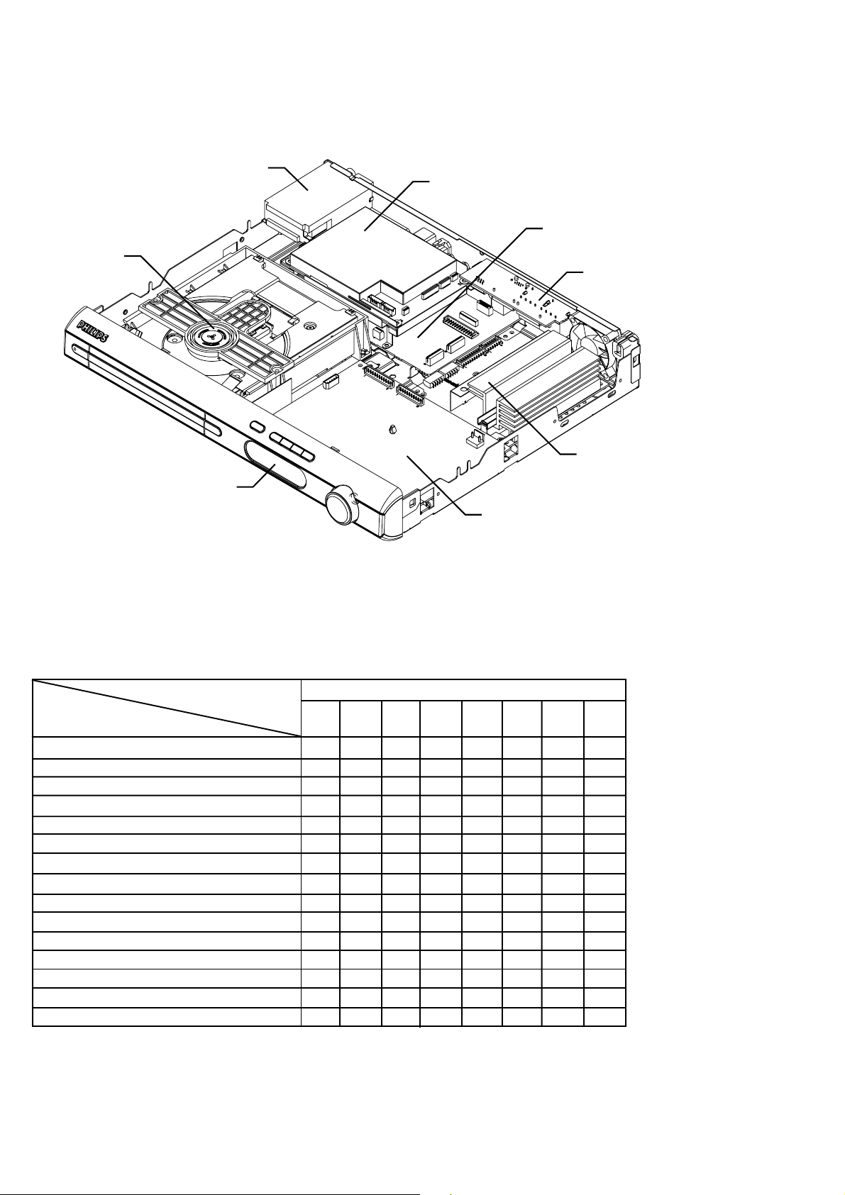
LOCATION OF PC BOARDS
Tuner Module
DVD Loader
1-2
SD6.1 RX Board
AV Board
Speaker Connector
Board
Amplifier Board
Front Board
VERSION VARIATIONS:
Type /Versions: LX3950W
Features &
Board in used:
Progressive Scan
Voltage Selector
Digital In x
TV-In
Aux-In x
Line-Out x
CVBS Output x
S-Video Output x
SCART Output x
Y/Pb/Pr (YUV) Component Video Output
ECO Standby x
PSU Board
/01
Page 3

SPECIFICATIONS
1-3
GENERAL:
Mains voltage : 120V for /17
220-240V for /01/05/75
110-127V/220-240V Switchable for /69
Mains frequency : 50/60Hz
Power consumption : < 0.6W at ECO Standby
< 80W at 1/8 P
rated
Dimension centre unit : 360 x 55 x 325mm
TUNER:
FM
Tuning range : 87.5-108MHz
Grid : 50kHz
100kHz for /17/69
IF frequency : 10.7MHz ± 25kHz
Aerial input : 75Ω coaxial
Sensitivity at 26dB S/N : < 7µV
Selectivity at 600kHz bandwidth : > 25dB
IF rejection : > 60dB
Image rejection : > 25dB
Distortion at RF=1mV, dev. 75kHz : < 3%
-3dB Limiting point : 8µV
Crosstalk at RF=1mV, dev. 40kHz : > 18dB
MW
Tuning range : 531-1602kHz
530-1700kHz for /17/69
Grid : 9kHz
10kHz for /17/69
IF frequency : 450kHz ± 1kHz
Aerial input : Frame aerial
Sensitivity at 26dB S/N : < 4.0mV/M
Selectivity at 18kHz bandwidth : > 20dB
IF rejection : > 45dB
Image rejection : > 28dB
Distortion at RF=50mV, m=80% : < 5%
Input sensitivity
Aux In : 1V ± 3dB at 39kΩ
Scart In : 500mV ± 3dB at 39kΩ
Output sensitivity
Line Out (Left/Right) : 0.7V ± 2dB at 47kΩ
Scart Out (Left/Right) : 0.6V ± 2dB at 10kΩ
COMPACT DISC/VCD/DVD:
Video Decoding : MPEG-2/MPEG-1/MPEG-4/Div X 4 & 5
Video DAC : 12 Bits
Signal System : PAL / NTSC
Video Format : 4:3 / 16:9
CVBS Out
1)
CVBS level : 1.0 ± 0.1V
p-p
Luminance S/N : >= 55dB
S-Video Out
1)
Y level : 1.0 ± 0.1V
p-p
Y S/N : >= 60dB
C level (burst) : 286mV
RGB/YUV Out
1)
Amplitude : 0.7 ± 0.1V
+1/-4 dB
p-p
p-p
S/N : >= 60dB
1)
Output terminals to be terminated with 75Ω
AMPLIFIER:
Output power
Front : 50W RMS / channel
Rear : 50W RMS / channel
Centre : 50W RMS
Subwoofer : 75W RMS
Frequency response ±3dB : 20Hz-20kHz
Hum (Volume Minimum) : 200nW
Residual noise (Volume Minimum) : 40nW
Page 4

MEASUREMENT SETUP
Tuner FM
1-4
Bandpass
LF Voltmeter
e.g. PM2534
RF Generator
e.g. PM5326
DUT
250Hz-15kHz
e.g. 7122 707 48001
Ri=50Ω
S/N and distortion meter
e.g. Sound Technology ST1700B
Use a bandpass filter to eliminate hum (50Hz, 100Hz) and disturbance from the pilottone (19kHz, 38kHz).
Tuner AM (MW,LW)
RF Generator
e.g. PM5326
Ri=50Ω
DUT
Frame aerial
e.g. 7122 707 89001
Bandpass
250Hz-15kHz
e.g. 7122 707 48001
LF Voltmeter
e.g. PM2534
S/N and distortion meter
e.g. Sound Technology ST1700B
To avoid atmospheric interference all AM-measurements have to be carried out in a Faraday´s cage.
Use a bandpass filter (or at least a high pass filter with 250Hz) to eliminate hum (50Hz, 100Hz).
CD
Use Audio Signal Disc
(replaces test disc 3)
DUT
L
R
SBC429 4822 397 30184
S/N and distortion meter
e.g. Sound Technology ST1700B
LEVEL METER
e.g. Sennheiser UPM550
with FF-filter
Recorder
Use Universal Test Cassette CrO2 SBC419 4822 397 30069
or Universal Test Cassette
LF Generator
e.g. PM5110
Fe SBC420 4822 397 30071
DUT
L
R
S/N and distortion meter
e.g. Sound Technology ST1700B
LEVEL METER
e.g. Sennheiser UPM550
with FF-filter
Page 5
SERVICE AIDS
Service Tools:
Universal Torx driver holder .................................. 4822 395 91019
Torx bit T10 150mm ............................................. 4822 395 50456
Torx driver set T6 - T20 ......................................... 4822 395 50145
Torx driver T10 extended ...................................... 4822 395 50423
Compact Disc:
SBC426/426A Test disc 5 + 5A ............................ 4822 397 30096
SBC442 Audio Burn-in Test disc 1kHz ................. 4822 397 30155
SBC429 Audio Signals disc .................................. 4822 397 30184
Dolby Pro-logic Test Disc ...................................... 4822 395 10216
1-5
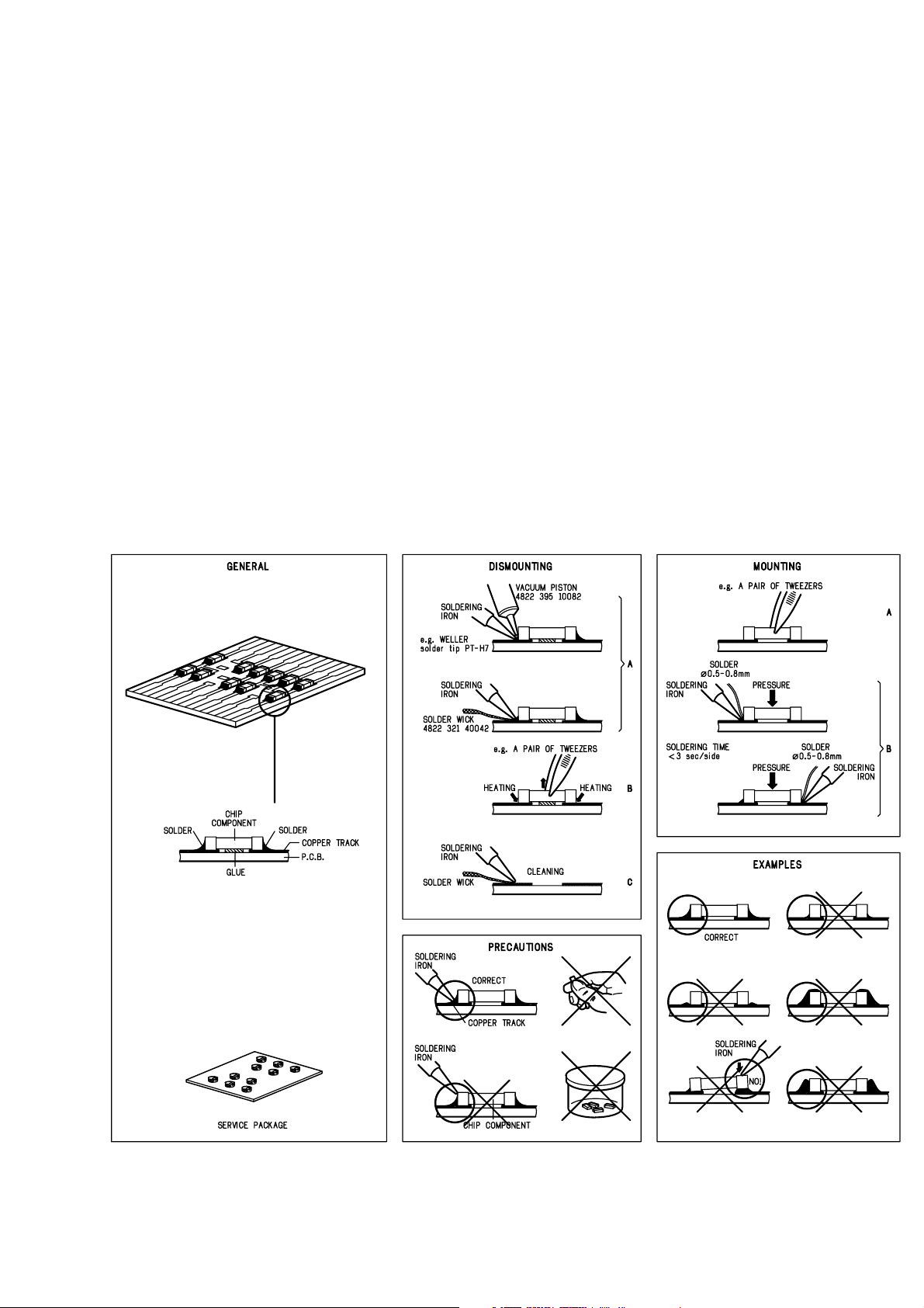
HANDLING CHIP COMPONENTS
Page 6
1-6
GB
All ICs and many other semi-conductors are
susceptible to electrostatic discharges (ESD).
Careless handling during repair can reduce life
drastically.
When repairing, make sure that you are
connected with the same potential as the mass
of the set via a wrist wrap with resistance.
Keep components and tools also at this
potential.
Tous les IC et beaucoup d’autres
semi-conducteurs sont sensibles aux
décharges statiques (ESD).
Leur longévité pourrait être considérablement
écourtée par le fait qu’aucune précaution n’est
prise à leur manipulation.
Lors de réparations, s’assurer de bien être relié
au même potentiel que la masse de l’appareil et
enfiler le bracelet serti d’une résistance de
sécurité.
Veiller à ce que les composants ainsi que les
outils que l’on utilise soient également à ce
potentiel.
F
WARNING
ATTENTION
GB
Complete Kit ESD3 (small tablemat, wristband,
connection box, extention cable and earth cable) ...........4822 310 10671
Wristband tester ....................................................................4822 344 13999
ESD
D
WARNUNG
Alle ICs und viele andere Halbleiter sind
empfindlich gegenüber elektrostatischen
Entladungen (ESD).
Unsorgfältige Behandlung im Reparaturfall kan
die Lebensdauer drastisch reduzieren.
Veranlassen Sie, dass Sie im Reparaturfall über
ein Pulsarmband mit Widerstand verbunden
sind mit dem gleichen Potential wie die Masse
des Gerätes.
Bauteile und Hilfsmittel auch auf dieses gleiche
Potential halten.
ESD PROTECTION EQUIPMENT:
NL
Alle IC’s en vele andere halfgeleiders zijn
gevoelig voor electrostatische ontladingen (ESD).
Onzorgvuldig behandelen tijdens reparatie kan
de levensduur drastisch doen verminderen.
Zorg ervoor dat u tijdens reparatie via een
polsband met weerstand verbonden bent met
hetzelfde potentiaal als de massa van het
apparaat.
Houd componenten en hulpmiddelen ook op
ditzelfde potentiaal.
Tutti IC e parecchi semi-conduttori sono
sensibili alle scariche statiche (ESD).
La loro longevità potrebbe essere fortemente
ridatta in caso di non osservazione della più
grande cauzione alla loro manipolazione.
Durante le riparazioni occorre quindi essere
collegato allo stesso potenziale che quello della
massa dell’apparecchio tramite un braccialetto
a resistenza.
Assicurarsi che i componenti e anche gli utensili
con quali si lavora siano anche a questo
potenziale.
WAARSCHUWING
I
AVVERTIMENTO
GB
Safety regulations require that the set be restored to its original
condition and that parts which are identical with those specified,
be used
Safety components are marked by the symbol
!
.
NL
Veiligheidsbepalingen vereisen, dat het apparaat bij reparatie in
zijn oorspronkelijke toestand wordt teruggebracht en dat onderdelen,
identiek aan de gespecificeerde, worden toegepast.
De Veiligheidsonderdelen zijn aangeduid met het symbool
!
F
Les normes de sécurité exigent que l’appareil soit remis à l’état
d’origine et que soient utiliséés les piéces de rechange identiques
à celles spécifiées.
Less composants de sécurité sont marqués
!
D
Bei jeder Reparatur sind die geltenden Sicherheitsvorschriften zu
beachten. Der Original zustand des Geräts darf nicht verändert werden;
für Reparaturen sind Original-Ersatzteile zu verwenden.
Sicherheitsbauteile sind durch das Symbol
!
markiert.
I
Le norme di sicurezza esigono che l’apparecchio venga rimesso
nelle condizioni originali e che siano utilizzati i pezzi di ricambio
identici a quelli specificati.
Componenty di sicurezza sono marcati con
!
CLASS 1
LASER PRODUCT
GB
Invisible laser radiation when open.
Avoid direct exposure to beam.
Osynlig laserstrålning när apparaten är öppnad och spärren
är urkopplad. Betrakta ej strålen.
SF
Avatussa laitteessa ja suojalukituksen ohitettaessa olet alttiina
näkymättömälle laserisäteilylle. Älä katso säteeseen!
DK
Usynlig laserstråling ved åbning når sikkerhedsafbrydere er
ude af funktion. Undgå udsaettelse for stråling.
S
Warning !
Varning !
Varoitus !
Advarse !
GB
After servicing and before returning set to customer perform a leakage
current measurement test from all exposed metal parts to earth ground to
assure no shock hazard exist. The leakage current must not exceed
0.5mA.
F
"Pour votre sécurité, ces documents doivent être utilisés par
des spécialistes agréés, seuls habilités à réparer votre
appareil en panne".
Page 7

DISMANTLING INSTRUCTIONS
Dismantling of the DVD Loader
2-1 2-1
1) The tray can be manually open by inserting a minus
screw driver and push the lever in the direction as shown
in Figure 1 to unlock the tray before sliding it out.
2) Slide out the tray and remove the Cover Tray assembly
(pos 110 + pos 111 + pos 112) as shown in Figure 2.
3) Loosen 5 screws to remove the Cover Top (pos 240).
- 1 screw each on the left & right side (pos 272)
- 3 screws on the rear (pos 270)
4) Loosen 4 screws D (see Figure 5) to remove the DVD
Loader (pos 1103-0001).
Figure 4
Figure 2Figure 1
Dismantling of the Tuner Module & Speaker Connector Board
1) Loosen 2 screws A (see Figure 4) to remove the Tuner
Module (pos 1105).
2) When the Tuner Module (pos 1105) become defective
and need to be replaced, make sure the Lug of the Tuner
Module is bend as shown in Figure 3.
Note : The Lug of the Tuner Module is purposely bend in
this way (see Figure 3) to prevent damage to the
Flex Cable.
3) Loosen 2 screws B (see Figure 4) to remove the Speaker
Connector Board (pos 1102).
Dismantling of the PSU Board, Amplifier Board, SD6.1 RX Board & AV Board
1) Loosen 4 screws E and uncatch C1 (see Figure 5) to
remove the PSU Board (pos 1104).
4) Loosen 2 screws H and uncatch C2 (see Figure 6) to
remove the Shield AV (pos 180).
Figure 5
Figure 3
2) Loosen 4 screws F (see Figure 5) to remove the Amplifier
Board (pos 1107).
3) Loosen 2 screws G (see Figure 5) to remove the SD6.1
RX Board (1103-1001).
5) Loosen 5 screws C (see Figure 4) and uncatch 2 catches
C3 (see Figure 7) to remove the AV Board (pos 1101).
Figure 6
Figure 7
Page 8
SERVICE POSITIONS
SD6.1 RX Board AV Board Thick Insulation Sheet Speaker Connector BoardAmplifier BoardThick Insulation Sheet
2-2
2-2
Page 9
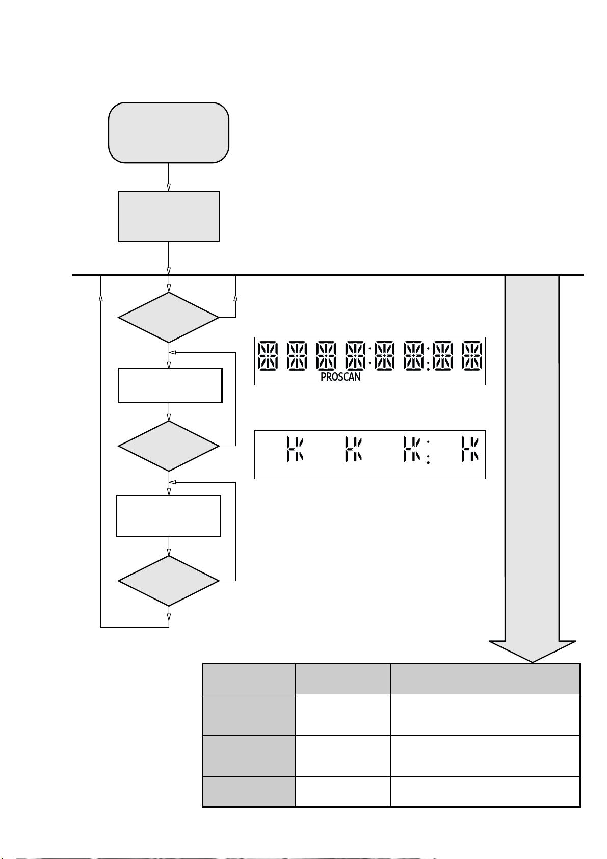
SERVICE TEST PROGRAM
To start service test program
hold S button depressed
while set is in standby
and press
the STANDBY button*
Display shows the
ROM version
"SVxx-yy"
MAIN MENU
DISPLAY
TEST
BII
Button pressed?
* Mains power to set must be on
H
S refers to Service Mode
V refers to Version
xx refers to Software version number of the back uProcessor
(counting up from 01 to 99)
yy refers to the front uProcessor version number
(00 will be displayed if there is no front uProcessor use)
N
3-1
old S button depressed
till the Display shown "SVxx-yy"
Y
Display shows Figure 1
BII
Button pressed?
Y
Display shows Figure 2
9
Button pressed?
Y
Figure 1
N
Figure 2
N
Various
other Tests
TEST
EEPROM FORMAT
TEST
ROTARY
ENCODER TEST
LEAVE SERVICE
TEST PROGRAM
Activated with
S
S to Exit
VOLUME
Knob
Disconnect
mains cord
ACTION
Load default data. Display shows "NEW".
Caution!
All presets from the customer will be lost!!
Display shows value for 2 seconds.
Values increases or decreases in steps of 1 until
0 (VOL MIN) or 40 (VOL MAX) is reached.
SD6.1 Service Test Program dd wk0405
Page 10

3-2
Procedure to change Tuner Grid (not for all versions)
1) Power up the set and select TUNER source.
2) Hold "PLAY" button depressed while set is in standby
and press the "STANDBY" button.
3) Hold "PLAY" button depressed till the display shown
'PHILIPS->FM' followed by display the new tuning grid
'GRID 9' or 'GRID 10'.
Note: Repeating the same action will toggle back to its
previous tuning grid setting.
Reprogramming of DVD version Matrix
After repair, the customer setting and region code may be
lost. Reprogramming will put the set back in the state in
which it has left the factory, ie. with the default setting and
the allowed region code.
To reprogram do as follows:
1) Power up the set and select DISC source.
2) Open tray by press "OPEN/CLOSE" button on the set
or press and hold "STOP" button on the RC.
3) Press the following buttons on the Remote Control:
<9> <9> <9> <9> <AUDIO> <1> ......... for LX3900SA/01
<9> <9> <9> <9> <AUDIO> <2> ......... for LX3900SA/05
<9> <9> <9> <9> <AUDIO> <3> ......... for LX3900SA/69
<9> <9> <9> <9> <AUDIO> <4> ......... for LX3900SA/75
<9> <9> <9> <9> <AUDIO> <5> ...........for LX3950W/01
<9> <9> <9> <9> <AUDIO> <6> ...........for LX3950W/05
4) The display shows 'YYYY-ZZ' and the tray will close.
YYYY = model number (eg. 3900, 3950, etc.)
ZZ = stroke version (eg. 01, 05, etc.)
Procedure for check Software version
1) Power up the set and select DISC source.
2) Open tray by press "OPEN/CLOSE" button on the set
or press and hold "STOP" button on the RC.
3) Press "OSD" button on the Remote control.
4) The TV screen will shows:
SD6.1 Vxx YYYY-ZZ P QQ
SERVO: GGGGGGGG REG:D
Procedure to upgrade software
1) Power up the set and select DISC source.
2) Open tray by press "OPEN/CLOSE" button on the set
or press and hold "STOP" button on the RC.
3) Place upgrade CD-ROM onto tray and close.
4) The set will response and display the following:
- LOAD [After the disc is read, the tray will open for
you to remove the disc]
- ERASE
- WRITE
- ERROR [if upgrade is unsuccessful]
- UPG END -> PHILIPS [if upgrade is successful]
- DISC->CLOSE->LOAD [Tray will close indicating
that the upgrade process is completed]
5) The whole process should not take more than 5
minutes.
Caution: Do not unplug the set until upgrade is completed.
Trade Mode
Trade mode is a feature that will block all set keys when
enabled. It is for dealers to prevent customers from
removing disc, changing source etc using the set keys.
Rotary and Remote Control (RC) keys are still allowed in
Trade mode.
To activate Trade Mode:
1) Power up the set and select DISC source.
2) Open tray by press "OPEN/CLOSE" button on the set
or press and hold "STOP" button on the RC.
3) Then press buttons <2> <5> <9> on the RC.
4) The display shows 'TRA ON' and the tray will close.
Trade Mode is now enabled.
To deactivate Trade Mode:
1) Power up the set and select DISC source.
2) Open tray by press and hold "STOP"button on the RC.
3) Then press buttons <2> <5> <9> on the RC.
4) The display shows 'TRA OFF' and the tray will close.
Trade Mode is now disabled.
xx = version number
YYYY = model number (eg. 3900, 3950, etc.)
ZZ = stroke version (eg. 01, 05, etc.)
P / D = region code
QQ = version number of front uProcessor
GGGGGGGG = version for servo code
Page 11

SET BLOCK DIAGRAM
4-1
4-1
TUNER
(TM 08)
74HC4052
1n0
650mV
10K
2.5V
78dBA
3.2dB
78dBA
3.2dB
HEADPHONE
TDA8920
L/R
RDS IC
POWER AMP
SAA6581T
10K
TDA8920
SURROUND
POWER AMP
1/2xTDA8920
2C45
1/2XTDA8920
SCL
SDA
M62320FP
SCL
SDA
VDD
GND
CS0
CS1
CHIP SELECT
I2C BUS
TRANSCEIVER
PWR
OUT I/O IN
RES
D5
D6
D7
CS2
SHIFT
REG
8
88
DATA LATCHES
88 8
I/O PORT
D1
D2
D3
D4
A3B
1
VS
OUT
GND
SO
D0
32.767 kHz
4MHz
Block Diagram_3139 119 37581_dd wk0402
Page 12
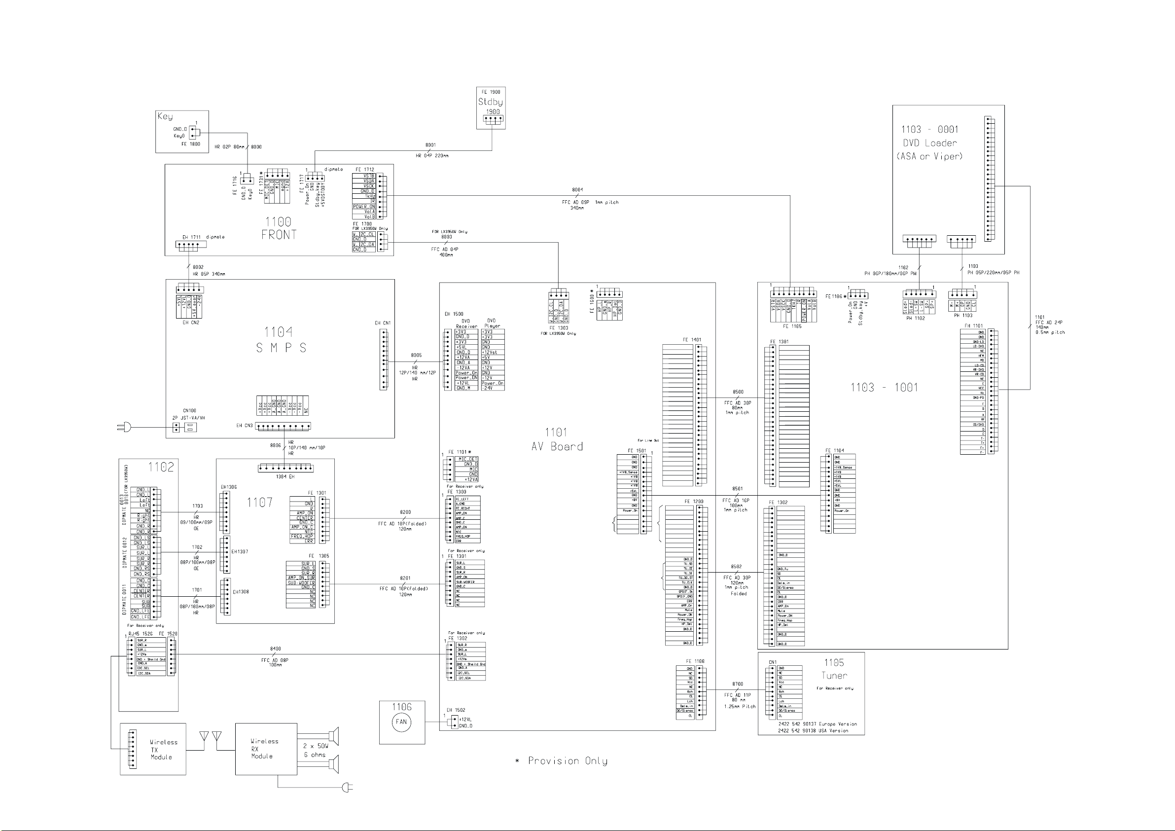
SET WIRING DIAGRAM
5-1
5-1
26
1
1
( Display Board )
1
1
11
1
GND
P50
NC / Line 2
Data for
To Tuner
SCART1/Line3
SCART0/Line3
PCMDATA_LO
SPDIF_PCM_Data_MIC_IN
PCM_Data_LR
PCM_Data_sLR
PCM_Data_Sub/Cen
PCM_Data_EX_sLR (op)
ADC
AV_MUTE
CVBS_REF
PCMLRCLK
PCMCLK
PCMSCLK
SPDIF_out
SCL-DAC
SDA-DAC
Mic_det
Y_REF
Y
C_REF
C
CVBS
G_REF
G_Y
B_REF
B_U
R_REF
R_V
GND
GND
GND
GND
GND
1
GND
GND
GND
GND
GND
( PSU Board )
1
1
1
1
1
1
Amplifier
Board
1
1
1
DAC_STB
To control
VSCK
DAC
VSDA
GND
1
GND
P50
NC / Line 2
SCART1/Line3
SCART0/Line3
AV_MUTE
Y_REF
Y
C_REF
C
CVBS_REF
CVBS
G_REF
G_Y
B_REF
B_U
R_REF
R_V
GND
PCMLRCLK
PCMDATA_LO
GND
PCMCLK
PCMSCLK
GND
SPDIF_out
GND
SPDIF_PCM_Data_MIC_IN
GND
Mic_det
GND
PCM_Data_LR
GND
PCM_Data_sLR
GND
PCM_Data_Sub/Cen
GND
PCM_Data_EX_sLR (op)
GND
PCMDATA_in
SCL-DAC
SDA-DAC
SD6.1 RX Board
DAC_STB
VSCK
VSDA
GND
26
1
Speaker
Connector
Board
RDS_CLK
RDS_DAT
Note : Some values may varies, see respective parts
list and circuit diagram for correct value.
RDS_CLK
RDS_DAT
1
1
Wiring Diagram_3139 119 37571_dd wk0407
Page 13

6-1 6-1
FTD DISPLAY PIN CONNECTION
8G 7G 6G 5G 4G 3G 2G 1G
FRONT BOARD
TABLE OF CONTENTS
FTD Display Pin Connection ........................................... 6-1
Display part - Top & Bottom View Layout ........................ 6-2
Display part - Circuit Diagram ......................................... 6-3
Key part - Layout & Circuit diagram ................................ 6-4
Standby part - Layout & Circuit diagram ......................... 6-5
Electrical parts list............................................................ 6-5
Dp
col
( 1G - 8G )
col Dp
a
j
h
f
g
r
e
k
p
m
j
n
d
col
b
c
P1
P2
P3
P4
P5
P6
P7
P8
P9
P10
P11
P12
P13
P14
P15
P16
P17
8G
7G
a
j
h
k
b
f
m
g
c
e
r
n
d
-
p
-
a
j
h
k
b
f
m
g
c
e
r
n
d
p
col
Dp
6G
5G
a
j
h
k
b
f
m
g
c
e
r
n
d
p
a
j
h
k
b
f
m
g
c
e
r
n
d
p
-
4G
a
j
h
k
b
f
m
g
c
e
r
n
d
col
p
-
3G
2G
a
j
h
k
b
f
m
g
c
e
r
n
d
col
p
Dp
a
j
h
k
b
f
m
g
c
e
r
n
d
p
1G
a
j
h
k
b
f
m
g
c
e
r
n
d
-
p
-
Page 14

DISPLAY BOARD - TOP VIEW LAYOUT
This assembly drawing shows a summary of all possible versions. For components used in a specific version see schematic diagram and respective parts list.
6-2
6-2
DISPLAY BOARD - BOTTOM VIEW LAYOUT
This assembly drawing shows a summary of all possible versions. For components used in a specific version see schematic diagram and respective parts list.
3139 113 3531 pt4 dd wk0403
3139 113 3531 pt4 dd wk0403
Page 15
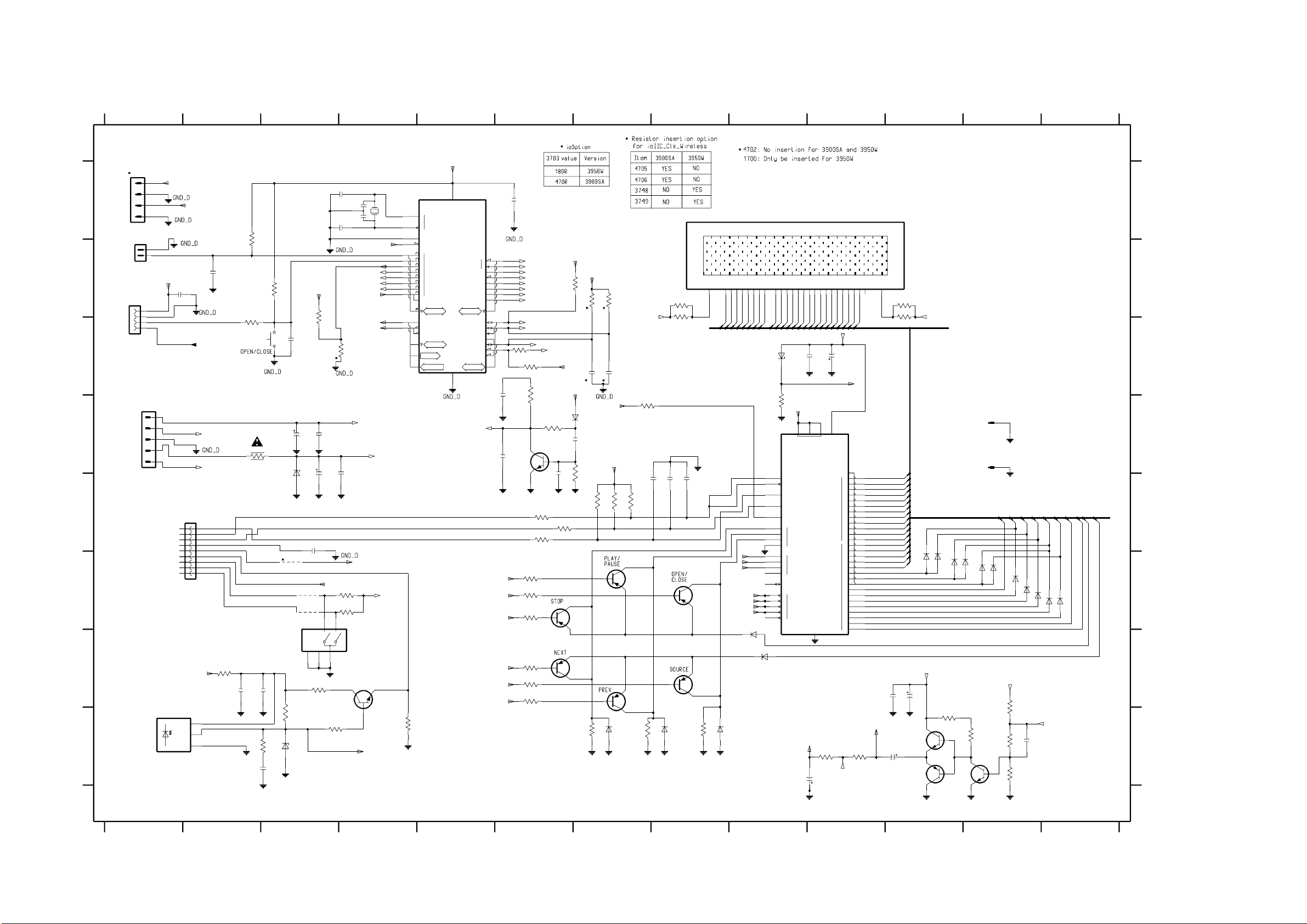
DISPLAY BOARD - CIRCUIT DIAGRAM
6-3 6-3
12345678910111213
DISPLAY BOARD
7700
10K
1
XTAL
2
TEST
RST
0
1
2
3
AIN
4
5
6
7
VAREF
P6<0:7>
INT3
PDO
PWM
P5<0:1>
TC<3:4>
CLZ<0:1>
+5VDSTBY
2814
Φ
MC
0
INT
1
RD
DVO
P1<0:7>
SCK
SCL
SI
SO
SDA
STOP
INT5
P4<0:3>
RESET
ioPseudoKey_Play
ioPseudoKey_Open
ioPseudoKey_Stop
ioPseudoKey_Next
ioPseudoKey_Source
ioPseudoKey_Prev
19
20
21
22
23
24
25
26
15
16
17
18
2704
2709
1n
2702
3751 4K7
10n
10n
7701
BC847B
iocom_0
iocom_1
iocom_2
iocom_3
ioSW0
ioSW1
ioSW2
ioPseudoKey_Prev
ioPseudoKey_Next
ioIIC_Clk_Wireless
ioIIC_Data_Wireless
stdy
3750
1K
1K
3709
3711
680K
3717
100R
3720
100R
3721
4K7
3723
4K7
3725
4K7
3730
4K7
3734
4K7
3737
4K7
2713
3718
100R
+5VDSTBY
3747
+5VDSTBY
+5VDSTBY
6700
2708
10n
3713
BC857B
7705
7707
BC857B
+5VDSTBY
4K7
3748
2727
1N4148
100n
100K
3714
3741
4K7
100p
4K7
3749
2728
10K
6705
+5VL
+5VL
3715
4K7
100p
10K
3716
7703
BC857B
7712
BC857B
BZX79-C5V6
VGL+1
10K
3710
47K
3742
# 2729
4K7
100p
6706
# 2730
3705
33R
33R
3707
100p
# 2731
BZX79-C5V6
100p
4V8
3V3
7704
BC857B
7708
BC857B
3743
# : Provision
Note : Some values may varies, see respective
parts list for correct value.
P14
F1
1
G(1)
0V
0V
0V
4K7
6707
1G42G53G64G75G86G97G108G
G(3)
G(2)
G(4)
G(6)
G(5)
+5V
NW6312
ioSW0
ioSW1
ioSW2
iocom_0
iocom_1
iocom_2
iocom_3
6703
1N4148
BZX79-C5V6
11
G(8)
G(7)
UPD16311
6
5
9
8
52
10
11
12
13
2
3
4
7
50
49
48
47
46
6704
1N4148
P1515P1614P17
13
P(15)
P(17)
P(16)
6702
PDZ-6.2B
10K
3719
7702
CONTROLLER/
DIN
DOUT
STB
CLK
OSC
1
2
KEY
3
4
1
1
2
SWI
3
4
IC
1
2
3
LED
4
5
17
16
P(14)
P(13)
P(12)
2714
+5VL
143345
VDD
DRIVER
51
VGL+1
35V 10u
P(11)
FIP
VSS
Φ
P1020P1119P1218P13
P(10)
2724
P(9)
100n
P(7)
P(8)
2715
34
VEE
SEG<1:20>
GRID
3732
470R
P(6)
KS
-V_FIL
P(5)
35V 47u
-V_FIL
10
11
12
16
15
14
13
12
11
10
1702
20U26115TAN
P2
P3
F2
27P426P525P624P723P822P921
32P129
28
P(4)
P(3)
P(2)
P(1)
-24V
3706
33R
3708
VGL-1
33R
1703
1
SIN-01T-1.8
1704
BAS316
6712
7710
SIN-01T-1.8
BAS316
6713
3728
330R
1
G(8)
G(6)G(7)
BAS316
BAS316
6714
6715
+5VL
4K7
3726
4K7
3729
10K
3736
8239_210_97154...for 3139 113 3531 pt4_dd wk0403
G(5)
BAS316
6716
40kHZ
2719
BAS316
6717
22p
G(3)G(4)
BAS316
6718
G(2)
BAS316
6719
G(1)
P(1)
P(2)
15
P(1)
1
16
P(2)
2
17
P(3)
3
18
P(4)
4
19
P(5)
5
20
P(6)
6
21
P(7)
7
22
P(8)
8
P(9)
23
9
24
P(10)
25
P(11)
26
P(12)
27
P(13)
28
P(14)
29
P(15)
30
P(16)
31
P(17)
32
35
36
9
37
8
38
7
39
6
40
5
41
4
42
3
43
2
44
1
P(1)
P(2)
VGL-1
3733
470R
2720
10u
2716
35V
33n
2717
BC817-25
G(11)
7706
7709
BC857B
+12VL
47u 25V
BAS316
6709
BAS316
6710
G(10)
G(9)
G(8)
G(2)
G(1)
BAS316
6711
3727
330R
BC847B
FE-BT-VK-N
1700
W_I2C_CL
GND_D
A
W_I2C_DA
GND_D
B
C
D
E
F
G
H
1
2
3
4
1716
1
2
B2B-EH-A
To Key Board
1717
1
2
3
4
WH04D-1
To Standby Board
+5VL
+12VL
GND_D
+5V_Ever
From PSU Board
-24V
stdy
+5VDSTBY
DIPMATE
1711
1
2
3
4
5
VSTB
VSDA
VSCK
GND_MTK
40kHZ
ioSTBY
VOLA
VOLB
(SD6.1 RX Board)
To/From MPEG Board
TSOP4836ZC1
4
ioIIC_Clk_Wireless
ioIIC_Data_Wireless
2705
100n
Standbykey
1712
IR
09FMN-BTRK-A
+5VDSTBY
7713
VS
OUT
GND
5
1
2
3
4
5
6
7
8
9
+12VL
-24V
3
1
2
2732
100n
3731
100R
2721
2K7
3702
1K
100n
3712
4R7
3700
2722
3744
2726
1706
2K7
4u7
1K0
2n2
3701
6708
3738
2733
4702
100n
2706
6701
10K
PDZ-5.6B
+5VDSTBY
47u 25V
PDZ-5.6B
2725
22n
4700
4701
1713
EVEMC
2707
3735
3704
2710
1K2
2K7
1
A
2701
15p
2703
15p
ioPseudoKey_Stop
ioPseudoKey_Play
ioPseudoKey_Open
ioPseudoKey_Source
3703
470R
100n
2711
100n
47u 25V
stdy
3722
10K
3724
10K
3
B
C
245
3740
47K
ioOption
+5VDSTBY
+5VL
40kHZ
7711
BC847B
ioRC6
40KHZ
ioRC6
1701
CST
RESET
ioKey0
ioKey1
+5VDSTBY
+5VL
TMP87P809M
1
2
3
27
4
5
6
7
8
9
10
11
12
13
3739
1700 A1
1701 A4
1702 A11
1703 D12
1704 D12
1706 C3
1711 D1
1712 E2
1713 F3
1716 B1
1717 B1
2701 A4
2702 A6
2703 A4
A
2704 C6
2705 B1
2706 D3
2707 D3
2708 D6
2709 D6
2710 D3
2711 D3
2713 D6
2714 C9
2715 C10
2716 G11
B
2717 G11
2719 H12
2720 H11
2721 G2
2722 G2
2724 H10
2725 E3
2726 H2
2727 C7
2728 C7
2729 E7
C
2730 E8
2731 E8
2732 B2
2733 C3
3700 A2
3701 B3
3702 C2
3703 C3
3704 B3
3705 B8
3706 B11
3707 C8
D
3708 C11
3709 C6
3710 D7
3711 D6
3712 D2
3713 D6
3714 E7
3715 E7
3716 E7
3717 E6
3718 E6
3719 D9
E
3720 E6
3721 F6
3722 F4
3723 F6
3724 F4
3725 F6
3726 G12
3727 H11
3728 H12
3729 H12
3730 G6
F
3731 G2
3732 H10
3733 H10
3734 G6
3735 G3
3736 H12
3737 G6
3738 H3
3739 H4
3740 H3
3741 H7
3742 H7
G
3743 H8
3744 H2
3747 B6
3748 B7
3749 B7
3750 C6
3751 C6
4700 F3
4701 F3
4702 F3
6700 D6
6701 D3
H
6702 C9
6703 G9
6704 G9
6705 H7
6706 H8
6707 H8
6708 H3
6709 E11
6710 E11
6711 E11
6712 E11
6713 F12
6714 F12
6715 F12
6716 F12
6717 F12
6718 F13
6719 F13
7700 A5
7701 D6
7702 D9
7703 F7
7704 F8
7705 F6
7706 H11
7707 G6
7708 G8
7709 H11
7710 H12
7711 G4
7712 G7
7713 H1
12345678910111213
Page 16

6-4
6-4
KEY BOARD - COMPONENT LAYOUT
This assembly drawing shows a summary of all possible versions.
For components used in a specific version see schematic diagram and respective parts list.
KEY BOARD - CIRCUIT DIAGRAM
1800 A3 1801 B1 1802 B2 1803 B2 1804 B2 1805 B3 2800 B1 3802 A2 3803 A2 3804 A2 3805 A3
3139 113 3531 pt4 dd wk0403
KEY BOARD - CHIP LAYOUT
This assembly drawing shows a summary of all possible versions.
For components used in a specific version see schematic diagram and respective parts list.
3139 113 3531 pt4 dd wk0403
A
B
1234
1800
100p
GND_D
2800
1801
GND_D
3802
390R
1802
GND_D GND_DGND_DGND_D
3803
270R
1803
3804
220R
1804
1
2
3805
150R
1805
S2B-EH
KEY0
GND_D
A
B
Note : Some values may varies, see respective parts list for correct value.
1234
8239_210_97184...for 3139 113 3531 pt4_dd wk0403
Page 17

6-5
6-5
STANDBY BOARD - COMPONENT LAYOUT STANDBY BOARD - CHIP LAYOUT
This assembly drawing shows a summary of all possible versions.
For components used in a specific version see schematic diagram
and respective parts list.
3139 113 3531 pt4 dd wk0403
This assembly drawing shows a summary of all possible versions.
For components used in a specific version see schematic diagram
and respective parts list.
3139 113 3531 pt4 dd wk0403
STANDBY BOARD - CIRCUIT DIAGRAM
1900 A1 1901 A1 2900 A2 3900 B2 3901 A3 6900 B3 7900 B3
123
Note : Some values may varies, see respective parts list for correct value.
1900
100p
ioSTBY
GND_D
2900
5VDSTBY
1K0
3901
A
1
2
3
4
B4B-EH-A
Standbykey
1901
GND_D
5VDSTBY
B
3900
12K
7900
BC847B
6900
LTL-816EELC
GND_D
8239_210_97164...for 3139 113 3531 pt4_dd wk0403
123
A
B
ELECTRICAL PARTS LIST - FRONT BOARD
MISCELLANEOUS
1700 4822 267 10733 Flex Connector 4P
1701 2422 540 98518 RES CER 8MHz
1702 3139 111 04131 FTD HUV-08SS57T
1706 4822 276 13775 Tact Switch
1712 2422 025 16586 Flex Connector 9P
1713 2422 129 16975 Rotary Encoder 12P
1801 4822 276 13775 Tact Switch
1802 4822 276 13775 Tact Switch
1803 4822 276 13775 Tact Switch
1804 4822 276 13775 Tact Switch
1805 4822 276 13775 Tact Switch
1901 4822 276 13775 Tact Switch
CAPACITORS
2701 4822 122 33752 15pF 5% 50V
2702 3198 016 31020 1nF 25V
2703 4822 122 33752 15pF 5% 50V
2704 5322 126 11583 10nF 10% 50V
2706 4822 124 40433 47uF 20% 25V
2707 2238 586 59812 100nF +80/-20% 50V
2708 2238 586 59812 100nF +80/-20% 50V
2709 5322 126 11583 10nF 10% 50V
2710 4822 124 40433 47uF 20% 25V
2711 2238 586 59812 100nF +80/-20% 50V
2713 5322 126 11583 10nF 10% 50V
2714 2238 586 59812 100nF +80/-20% 50V
2715 3198 028 44790 47uF 20% 35V
2716 4822 126 14549 33nF 16V
2717 4822 124 12233 47uF 20% 25V
2719 4822 122 33761 22pF 5% 50V
2720 3198 028 41090 10uF 20% 35V
2721 2238 586 59812 100nF +80/-20% 50V
2722 2020 552 96305 4,7uF +80/-20% 10V
2724 3198 028 41090 10uF 20% 35V
2725 2238 916 15641 22nF 10% 25V
2726 4822 126 14238 2,2nF 50V
2727 2020 552 94427 100pF 5% 50V
2728 2020 552 94427 100pF 5% 50V
2732 2238 586 59812 100nF +80/-20% 50V
2733 2238 586 59812 100nF +80/-20% 50V
2800 2020 552 94427 100pF 5% 50V
2900 2020 552 94427 100pF 5% 50V
RESISTORS
3700 4822 051 30272 2k7 5% 0,062W
3701 4822 051 30272 2k7 5% 0,062W
3702 4822 051 30151 150R 5% 0,062W
3703 4822 051 30181 180R 5% 0,062W
3704 4822 051 30272 2k7 5% 0,062W
3705 4822 051 30339 33R 5% 0,062W
3706 4822 051 30339 33R 5% 0,062W
3707 4822 051 30339 33R 5% 0,062W
3708 4822 051 30339 33R 5% 0,062W
3709 4822 051 30102 1k 5% 0,062W
3710 4822 117 12925 47k 1% 0,063W
3711 4822 051 30684 680k 5% 0,062W
3712 4822 117 11152!4R7 5%
3713 4822 117 10837 100k 1% 0,1W
3714 4822 051 30103 10k 5% 0,062W
3715 4822 051 30103 10k 5% 0,062W
3716 4822 051 30103 10k 5% 0,062W
3717 4822 051 30101 100R 5% 0,062W
3718 4822 051 30101 100R 5% 0,062W
3719 4822 051 30103 10k 5% 0,062W
3720 4822 051 30101 100R 5% 0,062W
3721 4822 051 30472 4k7 5% 0,062W
3722 4822 051 30103 10k 5% 0,062W
3723 4822 051 30472 4k7 5% 0,062W
3724 4822 051 30103 10k 5% 0,062W
3725 4822 051 30472 4k7 5% 0,062W
3726 4822 051 30472 4k7 5% 0,062W
3727 4822 051 30331 330R 5% 0,062W
3728 4822 051 30331 330R 5% 0,062W
3729 4822 051 30472 4k7 5% 0,062W
3730 4822 051 30472 4k7 5% 0,062W
3731 4822 051 30101 100R 5% 0,062W
3732 4822 051 30471 470R 5% 0,062W
3733 4822 051 30471 470R 5% 0,062W
3734 4822 051 30472 4k7 5% 0,062W
3735 4822 117 11817 1k2 1% 1/16W
3736 4822 051 30103 10k 5% 0,062W
3737 4822 051 30472 4k7 5% 0,062W
3738 4822 051 30103 10k 5% 0,062W
3739 4822 051 30103 10k 5% 0,062W
3740 4822 117 12925 47k 1% 0,063W
3741 4822 051 30472 4k7 5% 0,062W
3742 4822 051 30472 4k7 5% 0,062W
3743 4822 051 30472 4k7 5% 0,062W
3744 4822 051 30102 1k 5% 0,062W
3747 4822 051 30472 4k7 5% 0,062W
3748 4822 051 30472 4k7 5% 0,062W
3749 4822 051 30472 4k7 5% 0,062W
3750 4822 051 30102 1k 5% 0,062W
3802 4822 051 30391 390R 5% 0,062W
3803 4822 051 30271 270R 5% 0,062W
3804 4822 051 30221 220R 5% 0,062W
3805 4822 051 30151 150R 5% 0,062W
3900 4822 051 30123 12k 5% 0,062W
3901 4822 051 10102 1k 2% 0,25W
4700 4822 051 30008 0R Jumper 0603
4701 4822 051 30008 0R Jumper 0603
4901 4822 051 20008 0R Jumper 0805
Page 18

ELECTRICAL PARTS LIST - FRONT BOARD
DIODES
6700 4822 130 30621 1N4148
6701 3198 020 55680 DIO REG SM PDZ5.6B
6702 9340 548 54115 DIO REG SM PDZ6.2B
6703 4822 130 30621 1N4148
6704 4822 130 30621 1N4148
6705 4822 130 34173 BZX79-C5V6
6706 4822 130 34173 BZX79-C5V6
6707 4822 130 34173 BZX79-C5V6
6708 3198 020 55680 DIO REG SM PDZ5.6B
6709 4822 130 11397 BAS316
6710 4822 130 11397 BAS316
6711 4822 130 11397 BAS316
6712 4822 130 11397 BAS316
6713 4822 130 11397 BAS316
6714 4822 130 11397 BAS316
6715 4822 130 11397 BAS316
6716 4822 130 11397 BAS316
6717 4822 130 11397 BAS316
6718 4822 130 11397 BAS316
6719 4822 130 11397 BAS316
6900 9322 179 76676 LED VS LTL-816EELC
6-6 6-6
TRANSISTORS & INTEGRATED CIRCUITS
7700 3139 240 50831 TMP87C809BM -
'LX3950S50831'
7701 5322 130 60159 BC847B
7702 9322 202 26671 IC SM UPD16311GC-AB6
7703 4822 130 60373 BC857B
7704 4822 130 60373 BC857B
7705 4822 130 60373 BC857B
7706 4822 130 42804 BC817-25
7707 4822 130 60373 BC857B
7708 4822 130 60373 BC857B
7709 4822 130 60373 BC857B
7710 5322 130 60159 BC847B
7711 5322 130 60159 BC847B
7712 4822 130 60373 BC857B
7713 9322 185 95667 IR Receiver TSOP4836ZC1
7900 5322 130 60159 BC847B
Note : Only the parts mentioned in this list are normal
service spare parts.
Page 19

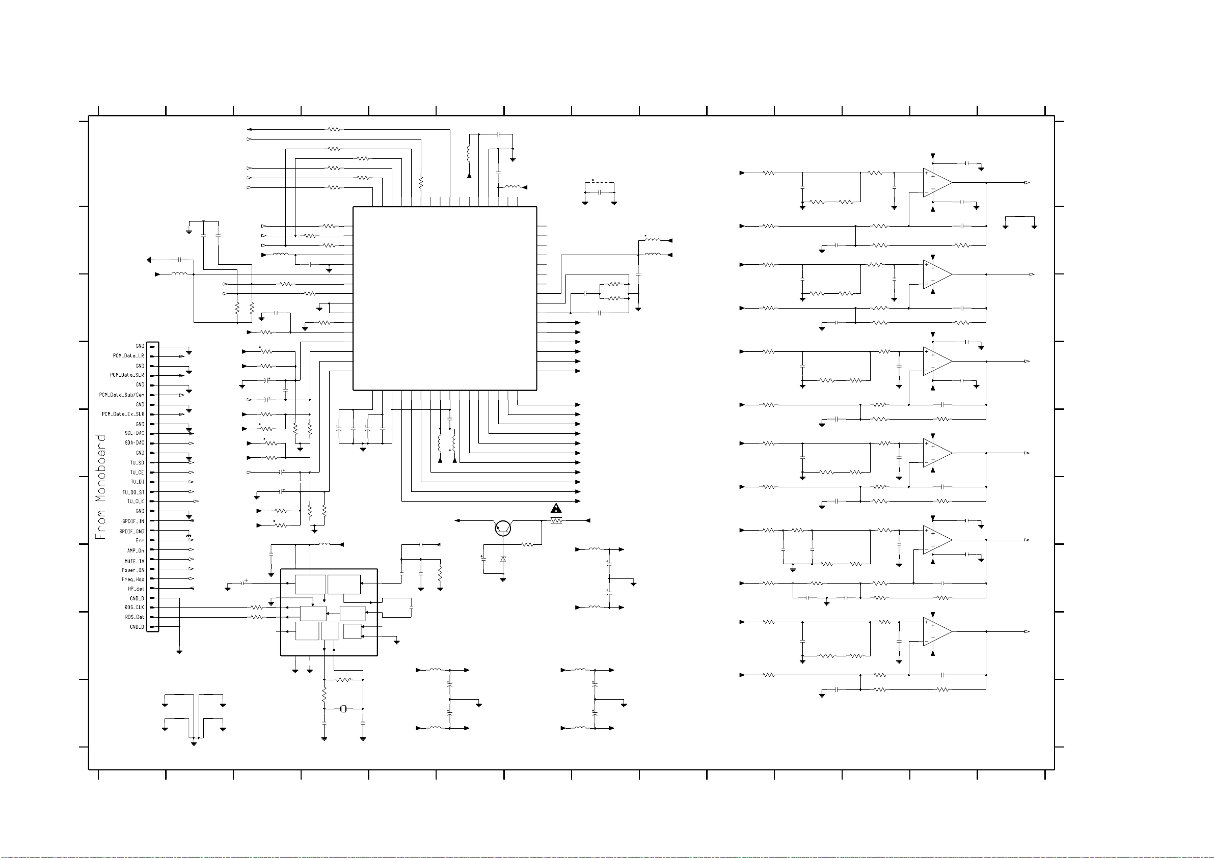
7-1 7-1
AV BOARD
BRIEF INTRODUCTION OF THE AV BOARD
The AV Board consists of the following features :
a. IC CS42418
IC CS42418 which includes functions such as ADC and DAC, sound control, volume control and muting function.
Sound features such as DSC are controllable via I2C Bus from the SD6.1 module.
The IC caters for 2 channels analog input via a 4 stereo channels MUX HEF4052BT.
The MUX multiplexed between Aux In, TV In, Tuner and Mic In.
Input networks are included to provide appropriate attenuation for various sources.
b.
SCART (for /01 and /05 versions only)
SCART input/output for audo/video (output only) connection to TV.
c. LINE OUT
Line out with cinch socket for connection to external amplifier.
TABLE OF CONTENTS
Brief Introduction of the AV Board ................................... 7-1
Top View Layout .............................................................. 7-2
Top & Bottom View Layout (Mapping) ............................. 7-3
Bottom View Layout ......................................................... 7-4
Circuit Diagram (Part 1) ................................................... 7-5
Circuit Diagram (Part 2) ................................................... 7-6
Circuit Diagram (Part 3) ................................................... 7-7
Circuit Diagram (Part 4) ................................................... 7-8
Circuit Diagram (Part 5) ................................................... 7-9
Circuit Diagram (Part 6) ................................................. 7-10
Electrical parts list.......................................................... 7-11
d. TV IN
TV In cinch socket for connection to external TV input.
e. Y/Pb/Pr (not for /01 and /05 versions)
Y/Pb/Pr component video output with cinch socket for connection to TV.
Progressive Y/Pb/Pr is selected through RC.
IC M62320FP
f.
IC M62320FP which served as additional I/O port.
g. DIGITAL IN
Digital In with cinch socket for connection to Digital Out of other audio equipments.
The Digital In source is fed to the SD6.1 module for audio decoding.
Page 20

AV BOARD - TOP VIEW LAYOUT
This assembly drawing shows a summary of all possible versions. For components used in a specific version see schematic diagram and respective parts list. 3139 113 3532 pt5 dd wk0403
7-2
7-2
Page 21

AV BOARD - TOP VIEW LAYOUT (MAPPING)
7-3
7-3
AV BOARD - BOTTOM VIEW LAYOUT (MAPPING)
Page 22

AV BOARD - BOTTOM VIEW LAYOUT
This assembly drawing shows a summary of all possible versions. For components used in a specific version see schematic diagram and respective parts list. 3139 113 3532 pt5 dd wk0403
7-4 7-4
Page 23

AV BOARD - CIRCUIT DIAGRAM (PART 1)
7-5
7-5
12345678910111213
1101
SCART_TV_Left_In
1102
LPR6520-J920G
1100
1
2
3
4
5
1
3
2
11
10
9
8
7
6
5
4
3
2
1
GND_tu
GND_tu_mtk
GND_D
GND_mic
2113
GND_tv
FE-BT-VK-N
A
B
C
FE-BT-VK-N
D
E
F
SCART_TV_Right_In
G
LPR6520-J440G
H
I
Note : Some values may varies, see respective parts list for correct value.
12345678910111213
68p
GND_tv
1103 3
Tu_CLK
TU_DO_STEREO
TU_Dat_In
TU_CE
TU_RDS_IN
Tu_SD
2100
2101
1n
GND_tu
Mic_det
+12A
68p
2115
GND_tv
68p
2119
GND_tv
68p
2127
GND_tv
5
4
6
2
1
GND_aux
3116
560R
3117
560R
3122
560R
3129
560R
7100
BC547B
100u
6100
3100
1K2
3101
1K2
GND_tu
3105
1K5
1N4148
6101
BZX384-C9V1
3109
3111
3102
4K7
4K7
47K
GND_tu
2116
2120
3150
3155
3104
4R7
47K
47K
GND_tu
100p
GND_tv
100p
GND_tv
GND_aux
3103
3118
680R
3123
680R
BC847B
BC847B
47K
3110
3112
7105
7108
+12Va
56K
GND_mic
56K
GND_mic
3119
3124
2129
2137
2103
1u0
2105
220p
GND_mic
2108
1u0
2110
220p
GND_mic
2114
1u0
56K
GND_tv
2118
1u0
56K
GND_tv
3130
4K7
68p
2130
100p
GND_aux GND_aux
3136
4K7
68p
2138
100p
GND_aux
3146
3158
GND_aux
10K
3151
470R
3156
470R
10K
3131
5K6
3137
5K6
2145
7107
BC857B
50V
2u2
D
3132
GND_aux
3140
GND_aux
1100 A2
1101 C2
1102 E2
1103 H3
2100 C3
2101 C3
2102 C7
2103 C5
2105 C5
2108 D5
2110 D5
A
2113 E2
2114 E5
2115 E3
2116 E4
2118 E5
2119 F3
2120 F4
2122 E11
2124 F7
2125 F11
2127 F3
2128 G6
2129 G4
B
2130 G5
2131 G8
2132 G9
2133 G11
2134 G11
2135 G6
2136 G8
2137 H4
2138 H5
2139 H9
2140 H10
2141 H11
C
2142 I9
2143 I11
2144 I11
2145 I5
2146 I9
2147 I10
2148 I11
3100 A3
3101 A3
3102 A4
3103 A4
3104 B4
D
3105 B4
3106 B6
3107 C6
3108 D9
3109 C4
3110 C4
3111 D4
3112 D4
3114 D8
3116 D3
3117 E3
E
3118 E4
3119 E4
3120 E9
3121 E8
3122 E3
3123 E4
3124 F4
3125 F7
3128 F7
3129 F3
3130 G5
3131 G5
F
3132 G6
3133 G10
3134 G11
3135 G11
3136 G5
3137 G5
3138 G10
3139 G10
3140 H6
3141 H10
3142 H11
3143 H11
G
3144 H9
3145 H10
3146 H5
3147 H10
3148 H11
3149 H11
3150 I4
3151 H5
3152 I6
3153 I10
3154 I10
H
3155 I4
3156 I5
3157 I6
3158 I5
3159 I10
3160 I11
3161 I11
3162 I9
3163 I10
3164 I6
4100 B12
4101 B12
I
4102 C11
4103 C11
4104 C11
5102 E11
5103 F11
6100 C3
6101 C4
6102 I7
6103 I7
2134
2144
4102
4103
4104
2122
2125
GND_aux
GND_sel
GND_w
V
5102
100u
100u
5103
3135
1K5
330p
3143
1K5
3149
1K5
330p
3161
1K5
GND_tv
2u2
2u2
4100
GND_sel_out
4101
GND_A_REF
+12A
-12A
LO_Left_+
LO_Left_-
LO_Right_+
LO_Right_-
8239_210_97275 (AV Circuit 1)...for 3532 pt5 dd wk0403
GND_tu_mtk
GND_tu
GND_mic
MIC_L
3106
5K6
GND_sel
3107
-12A
50V1u0
6K8
2102
916
VDD
7102
HEF4052BT
LOGIC
GND_sel
LL
1
5
LH
HL
23
4
HH
12
LL
LH
14
15
HL
HH
11
VEE
VSS
7
8
3125
5K6
10
6
A_In
LSBMSB
H
L
H
L
GND_tu
GND_sel_out
13
GND_sel_out
Source_sel_A1
Source_sel_A0
3114
100K
3121
100K
3108
1K2
3120
1K2
GND_a
GND_scart
Left_In
+12Va_LO
Right_In
GND_a
+12A
-12Va_LO
2124
50V 1u0
6K8
3128
LINE_R
GND_sel
+12Va_LO
GND_a
GND_a
-12Va_LO
+12Va_LO
-12Va_LO
100n
2131
7104-A
NJM4556AM
1
2136
100n
7104-B
NJM4556AM
7
2139
47p
3144
12K
2146
47p
3162
12K
3
8
2
4
3133
15K
82p
2132
GND_OP_LO
3138
12K
3141
15K
3145
12K
82p
3147
15K
2142
5
8
6
4
GND_OP_LO
3153
12K
2140
470p
GND_OP_LO
3159
15K
3163
12K
2147
470p
GND_OP_LO
3139
12K
3154
12K
470p
3142
10K
470p
3160
10K
3134
10K
2133
GND_OP_LO
330p
2141
3148
10K
2143
GND_OP_LO
330p
2148
2128
1u0
27K
2135
1u0
27K
GND_sel
LINE_L
+3V3
3152
470R
3157
470R
3164
470R
6102
1N4148
6103
BAS316
AV_Mute
Mute_LO
7100 B3
7102 C7
7104-A G9
7104-B H9
7105 I4
7107 H5
7108 I4
Page 24
AV BOARD - CIRCUIT DIAGRAM (PART 2)
7-6
7-6
1234567891011121314
PCM_Data_Mic_In
A
B
2209
D
100n
+3V3
5204
D
2276
SCL_DAC
SDA_DAC
PCM_Data_Sub_Cen
PCM_Data_SLR
PCM_Data_LR
2277
100p
C
1200
1
2
3
D
4
5
6
7
8
9
10
E
11
12
13
14
15
16
17
F
F
18
19
20
21
22
23
24
G
25
26
27
D
PCM_Data_LR
D
PCM_Data_SLR
D
PCM_Data_Sub_Cen
D
PCM_Data_EX_SLR
D
SCL_DAC
SDA_DAC
D
Tu_SD
TU_CE
TU_Dat_In
TU_DO_STEREO
TU_CLK
GND_tu_mtk
DIG_IN
GND_dig
PW_ERR
AMP_On
MUTE_TV
PWR_DN
Freq_Hop
HP_DET
28
29
30
H
D
I
GND_OP_LO
GND_OP_S
GND_OP_C
GND_OP
GND_A_REF
Note : Some values may varies, see respective parts list for correct value.
123456789101112 13 14
PCMCLK
PCMDATA_LO
PCM_BCLK
100p
PCM_LRCLK
3226
+3V3
+5VD
+5VA
GND_sel_out
Right_In
+5VA
+5VD
+5VD
+5VA
Left_In
GND_sel_out
+5VD
2251
D
2u2
2K2
+5VA
+3V3
3227
1200 C1
2200 A6
2201 A13
3200
33R
3201
33R
3202
33R
3203
33R
3206
33R
3208
33R
3211
1
DAC_SDIN1
33R
3214
33R
5202
2210
100n
3220
33R
3222
2288
2289
3259
100K
3294
100K
3
2
1
2222
50V
100n
VREF
SYNC
RDCL
RDDA
QUAL
33R
D
100p
3245
3244
100K
GND_A_REF
2235
100p
3260
GND_A_REF
5
12
POW SUPPL
RESET
RDS/RBDS
SIGNAL
QUALITY
DET
VSSA
VSSD
6
11
D
D
D
VDDAVDDD
&
DEM
2290
2K2
1u
D
3230
10K
3291
100K
3237
100K
2286
10u 50V
2287
50V10u
3240
100K
3292
100K
3293
100K
3251
100K
10u 50V
10u
2244
D
10
D
32751K0
16
32761K0
100K
100K
14
3233
5206
2u2
VSSA
10K
3261
3215
33R
OSC
CLK
&
13
2
3
4
5
D
6
7
8
9
10
11
12
13
14
15
16
50V
2228
4u7
100K
57 Khz
BANDPASS
(8th ORDER)
CLOCKED
COMP
TEST
CTRL
OSCO
OSCI
3287
DAC_SCLK
DAC_LRCK
VD_1
DGND_1
VLC
SCL_CCLK
SDA_CDOUT
AD1_CDIN
AD0_CS_
INT
RST_
AINR-
AINR+
AINL+
AINL-
2229
100n
GND_A_REF
+5VD
SAA6581T
SCOUT
2230
7207
MPX
CIN
TCON
MODE
64
DAC_SDIN2
17VQ18
10V
100u
63
2231
4
8
7
15
9
62
DAC_SDIN4
DAC_SDIN3
REFGND
FILT+
19
100n
220K
2K2
4M332
3290
5211
12
AT-51
2272
D
47p
2273
D
82p
33R
3207
57
58
59
60
61
OMCK
ADCIN2
ADCIN1
ADC_SCLK
ADC_LRCK
7103
CS42418
AOUTB4-21AOUTB4+22AOUTA4+23AOUTA4-24VA_125AGND_1
20
5205
+5VA
2240
1n
560p
2249
560p
2257
2250
D
D
3269
47p
D
5209
+12A
-12A
2u2
5212
2u2
56
ADC_SDOUT
2225
5218
+5VD
+5VA
TU_RDS_IN
10K
2263
2269
55
RMCK
AOUTB3-
26
100n
100u
100u
5200
+3V3
53
54
VLS
NC_3
AOUTB3+27AOUTA3+28AOUTA3-
2246
+12Va_Dif_LFE
GND_C
-12Va_Dif_LFE
2200
100n
100n
2203
51
52
VD_2
DGND_2
AOUTB2-30AOUTB2+31AOUTA2+
29
7205
BC547B
16V100u
6200
GND_A_REF
D
5201
49
50
NC_1
NC_2
32
BZX79-B5V6
GPO1
GPO2
GPO3
GPO4
GPO5
GPO6
GPO7
AGND_2
LPFLT
MUTEC
AOUTA1-
AOUTA1+
AOUTB1+
AOUTB1-
AOUTA2-
3266
1K2
+3V3
VA_2
48
47
46
45
44
43
42
41
40
39
38
37
36
35
34
33
+12A
-12A
3262
+12Va_Dif_LR
3210
1K8
3224
1K8
2256
470p
3239
1K8
3253
1K8
3268
18K
3283
1K8
3205
12K
3213
12K
3216
12K
12K
3219
3229
12K
3231
12K
3243
12K
3246
12K
3256
12K
3257
12K
3272
15K
3273
18K
GND_OP_C
3286
12K
3288
12K
12K
3236
GND_OP_S
12K
3250
GND_OP_S
3265
15K
3279
12K
100p
2205
2213
100p
2221
2234
2241
GND_OP_C
2260
3
2
-12Va_Dif_LR
+12Va_Dif_LR
5
6
-12Va_Dif_LR
+12Va_Dif_SLR
3
2
100p
-12Va_Dif_SLR
+12Va_Dif_SLR
5
6
100p
-12Va_Dif_SLR
+12Va_Dif_LFE
3
2
82p
-12Va_Dif_LFE
+12Va_Dif_LFE
5
6
100p
-12Va_Dif_LFE
DAC_L_+
D
4200
2202
100n
GND_A_REF
DAC_L_-
5219
+5VD
5203
+5VA
DAC_R_+
2211
100n
DAC_R_-
GND_A_REF
2214
2n2
Mutec
2216
680p
3221
3225
10K
10K
LO_Left_-
LO_Left_+
LO_Right_+
DAC_LS_+
LO_Right_-
DAC_L_-
DAC_L_+
DAC_LS_-
DAC_R_+
DAC_R_-
DAC_LS_-
DAC_LS_+
DAC_RS_+
DAC_RS_+
DAC_RS_-
DAC_C_-
DAC_C_+
DAC_LFE_+
DAC_RS_-
DAC_LFE_-
5207
2u2
+12Va
2248
DAC_LFE_+
+12Va_Dif_LR
100u
22R
+12A
DAC_LFE_-
GND_LR
100u
2254
-12A
5208
2u2
-12Va_Dif_LR
DAC_C_+
5210
2u2
5213
2u2
2265
2271
+12Va_Dif_SLR
100u
GND_S
100u
DAC_C_-
-12Va_Dif_SLR
3204
3212
3218
3228
3234
3241
3248
3254
3263
3270
3277
3284
5K6
2204
560p
3209
12K
GND_OP G ND_OP
5K6
560p
2208
GND_OP
5K6
2212
560p
3223
12K
GND_OP G ND_OP
5K6
5K6
2220
GND_OP_S
5K6
5K6
2233
GND_OP_S
5K6
3264
3K3
3K9
2242
330p
GND_OP_C
3K3
5K6
2259
GND_OP_C
5K6
330p
2255
GND_OP
560p
GND_OP_S
560p
GND_OP_S
2243
470p
3271
3K9
GND_OP_C
560p
GND_OP_C
560p
2217
12K
3238
2227
560p
3252
12K
2238
560p
3267
18K
3282
12K
2267
560p
100n
2201
8
7200-A
4
LM833D
1
100n
2206
2207
3217
GND_LR
L
GND_LR
47p
GND_HP
GND_LR
1K8
8
7200-B
7
LM833D
4
2215
47p
3232
1K8
100n
2218
8
7201-A
4
LM833D
1
100n
2223
GND_S
Ls
GND_S
2224
47p
3247
1K8
7201-B
8
4
8
4
LM833D
2236
47p
3258
1K8
7202-A
LM833D
7
100n
2239
GND_C
1
100n
2245
GND_C
Rs
Lfe
2252
82p
3274
18K
8
7202-B
7
LM833D
4
2261
47p
3289
1K8
8239_210_97275 (AV Circuit 2)...for 3532 pt5 dd wk0403
C
R
2202 A8
2203 A6
2204 A11
2205 A12
2206 A13
2207 B13
2208 B11
2209 B2
A
2210 B4
2211 C8
2212 C11
2213 C12
2214 C8
2215 C13
2216 C8
2217 C11
2218 D13
2220 D11
2221 D12
2222 D3
2223 D13
B
2224 D13
2225 E6
2227 E11
2228 E4
2229 E4
2230 E4
2231 E5
2233 E11
2234 E12
2235 F3
2236 F13
2238 F11
C
2239 F13
2240 F5
2241 G12
2242 G11
2243 G11
2244 G3
2245 G13
2246 G6
2248 G8
2249 G5
2250 G5
2251 G3
D
2252 G13
2254 G8
2255 G11
2256 G12
2257 G5
2259 H11
2260 H12
2261 H13
2263 I6
2265 I8
2267 I11
E
2269 I6
2271 I8
2272 I4
2273 I4
2276 B2
2277 B2
2286 D3
2287 D3
2288 E3
2289 F3
2290 C3
3200 A4
F
3201 A4
3202 A4
3203 A4
3204 A10
3205 A12
3206 A4
3207 A5
3208 A4
3209 A11
3210 A12
3211 B4
3212 B10
G
3213 B12
3214 B4
3215 B4
3216 B12
3217 B13
3218 B10
3219 B12
3220 C3
3221 C8
3222 C4
3223 C11
H
3224 C12
3225 C8
3226 C3
3227 C3
3228 C10
3229 C12
3230 C3
3231 C12
3232 C13
3233 C4
3234 D10
3236 D12
I
3237 D3
3238 D11
3239 D12
3240 E3
3241 D10
3243 D12
3244 E3
3245 E4
3246 E12
3247 E13
3248 E10
3250 E12
3251 E3
3252 E11
3253 E12
3254 F10
3256 F12
3257 F12
3258 F13
3259 F3
3260 F4
3261 F4
3262 F7
3263 F10
3264 F11
3265 F12
3266 F7
3267 G11
3268 G12
3269 G5
3270 G10
3271 G11
3272 G12
3273 G12
3274 G13
3275 G3
3276 G3
3277 H10
3279 H12
3282 H11
3283 H12
3284 H10
3286 H12
3287 H4
3288 I12
3289 I13
3290 I4
3291 D3
3292 E3
3293 E3
3294 F3
4200 A8
5200 A6
5201 A7
5202 B3
5203 B9
5204 B2
5205 E5
5206 F4
5207 G8
5208 G8
5209 H5
5210 H8
5211 I4
5212 I5
5213 I8
5218 E6
5219 B9
6200 G6
7103 C6
7200-A A13
7200-B B13
7201-A D13
7201-B E13
7202-A F13
7202-B H13
7205 F7
7207 G5
Page 25

AV BOARD - CIRCUIT DIAGRAM (PART 3)
7-7 7-7
12345678910111213
A
D
2326
SCL_DAC
B
SDA_DAC
+3V3
3312
33R
3313
33R
+3V3
25V47u
2307
100n
2306
D
C
D
1302
FE-BT-VK-N
1
2
3
4
5
6
7
8
+5VD
GND_S
GND_W
4300
2324
100n
E
F
G
H
I
Note : Some values may varies, see respective parts list for correct value.
12345678
100p
D
2325
6CH_SR
6CH_SL
M62320FP
100p
4301
1
2
3
4
FE-BT-VK-N
GND_C
GND_S
1303
2
3
13
8
7308
GND_D
D
SCL
SDA
VDD
GND
2312
GND_a
CS016CS115CS2
CHIP SELECT
2
I
C BUS
TRANSCEIVER
PWR
RES
DATA LATCHES
12
+5V
47u
22n
2313
GND_LR
14
SHIFT
REG
88
88 8
I/O PORT
8
INI/OOUT
D15D26D37D49D510D611D7
+5V
5301
2u2
47u
22n
2317
GND_W
2318
1300 A12
1301 D12
1302 F2
1300
2300
L
SO
1
D0
4
Source_sel_A0
Source_sel_A1
MUTE_LR_SUB
MUTE_SL_SR
MUTE_CEN
AMP_ON_LR_SUB
AMP_ON_SLR
Mute_LO
4302
+12Va
R
MUTE_LR_SUB
Ls
Rs
MUTE_SL_SR
Lfe
1u0
2303
1u0
+3V3
AV_Mute
Mutec
2308
1u0
2311
1u0
+3V3
AV_Mute
Mutec
C
+3V3
AV_Mute
MUTE_CEN
Mutec
3300
680R
GND_LR
3310
680R
6304
BAS316
6305
BAS316
6306
BAS316
3323
680R
GND_S
3334
680R
6307
BAS316
6308
BAS316
6309
BAS316
GND_C
6310
BAS316
6311
BAS316
6312
BAS316
2316
4303
7300
BC847B
BC847B
7303
7306
BC857B
3316
27K
3318
1K0
3320
1K0
3322
1K0
1u0
3338
3340
1K0
3342
1K0
3344
1K0
27K
3358
27K
3359
1K0
3360
1K0
3361
1K0
7310
BC847B
BC847B
7312
3346
680R
BC847B
BC847B
3356
680R
1u0
AMP_ON_LR_SUB
7314
BC857B
7317
7319
7321
BC857B
2304
D
2314
3304
1K0
3308
1K0
1u0
2305
AMP_ON
3327
1K0
3331
1K0
1u0
2315
D
AMP_On_SLR
3350
1K0
3354
1K0
2322
1u0
AMP_ON
1u0
D
2323
3301
680R
BAS316
BAS316
3324
680R
680R
1u0
3305
1K0
3309
1K0
3311
680R
Sub_Mute
6300
6301
3328
1K0
3332
1K0
BAS316
BAS316
3347
+5VD
3335
680R
6302
6303
3351
1K0
3355
1K0
+3V3
3321
+5VD
+3V3
3357
680R
3343
3302
BC847B
7301
2301
100p
3306
100R
3303
100R
1K8
1K8
3307
GND_LR
DVD_M_C
GND_C
7304
BC847B
4K7
3319
4K7
BC847B
7311
3314
1K0
3362
4K7
2302
BC857B
7307
3317
2309
100p
GND_LR
1K0
7309
BC847B
GND_LR
100p
3315
47K
GND_LR
3329
GND_LR
1K8
3330
NTC
Freq_Hop
PW_ERR
3325
100R
3326
100R
1K8
6CH_SL
6CH_SR
DVD_M_SUB
GND_S
GND_C
7313
2310
3336
1K0
3363
BC847B
7318
7320
BC847B
Sub_Mute
100p
GND_S
BC857B
7315
3337
GND_S
1K0
3339
7316
BC847B
4K7
GND_S
2319
100p
100p
2320
GND_C
GND_S
47K
3352
3348
100R
3349
100R
1K8
1K8
3353
DVD_M_C
DVD_M_SUB
GND_C
BC847B
4K7
3341
4K7
FE-BT-VK-N
1
2
3
4
5
6
7
8
9
10
1301
FE-BT-VK-N
1
2
3
4
5
6
7
8
9
10
8239_210_97275 (AV Circuit 3)...for 3532 pt5 dd wk0403
1303 G3
2300 A6
2301 A9
2302 A9
2303 B6
2304 C8
2305 C8
2306 B2
A
2307 B2
2308 D6
2309 D9
2310 E9
2311 E6
2312 E3
2313 E3
2314 F8
2315 F8
2316 G7
2317 G4
2318 G4
2319 G9
B
2320 H9
2322 I8
2323 I8
2324 H2
2325 A2
2326 A2
3300 A7
3301 A8
3302 A10
3303 A10
3304 A8
3305 A8
C
3306 A10
3307 A10
3308 A8
3309 A8
3310 B7
3311 B8
3312 B2
3313 B2
3314 B9
3315 B9
3316 B7
D
3317 C9
3318 C7
3319 C9
3320 C7
3321 C8
3322 C7
3323 D7
3324 D8
3325 D10
3326 D10
3327 D8
3328 D8
E
3329 D10
3330 D10
3331 E8
3332 E8
3334 E7
3335 E8
3336 F9
3337 F9
3338 F7
3339 F9
3340 F7
3341 F9
F
3342 F7
3343 F9
3344 F7
3346 G7
3347 G8
3348 G11
3349 G11
3350 G8
3351 G8
3352 G10
3353 G10
G
3354 H8
3355 H8
3356 H7
3357 H9
3358 I7
3359 I7
3360 I7
3361 I7
3362 C9
3363 F9
4300 G2
4301 E3
H
4302 G5
4303 H7
5301 G4
6300 C8
6301 C8
6302 F8
6303 F8
6304 C7
6305 C7
6306 C7
6307 F7
6308 F7
6309 F7
I
6310 I7
6311 I7
6312 I7
7300 A7
7301 A9
7303 A7
7304 A9
7306 B7
7307 B9
7308 A3
7309 C9
7310 D7
7311 D9
7312 E7
7313 E9
7314 E8
7315 E9
7316 F9
7317 G7
7318 G9
7319 H7
7320 H9
7321 H7
9 10111213
Page 26

AV BOARD - CIRCUIT DIAGRAM (PART 4)
7-8 7-8
A
B
C
D
E
F
1400 A12
1401 A1
1402 G12
1403 G12
1405-A E13
1405-B F12
1408 H5
1410 G2
1411 G2
2400 A6
2401 A8
2402 A10
2403 A11
2404 A11
2405 A8
2406 B11
2407 B8
2408 B11
2409 B7
2410 B10
2411 B8
2412 B6
2413 B11
2414 B13
2415 E7
2416 E5
2417 C13
2418 D12
2419 D13
2420 D6
2422 D12
2423 E4
2424 H11
2425 H12
2426 H12
2427 D8
2428 E8
2434 E11
2437 E11
2440 F1
2441 F11
2442 F12
2443 F12
2445 H7
2446 H6
3400 A7
3401 A8
3403 A7
3404 A12
3405 A6
3406 A10
3407 A6
3408 B12
3409 B7
3410 B11
3412 B7
3413 B8
3415 B7
3416 C11
3417 C9
3418 C10
3421 C10
3422 C11
3423 D6
3424 D10
3425 D4
3426 C5
3427 D6
3428 C5
3430 E6
3432 C5
3433 C5
3434 E4
3435 D5
3436 G11
3437 E4
3438 G11
3439 E5
3440 G11
3454 H5
3455 H5
4400 B13
4401 A10
4402 G11
4403 G11
4404 H11
4406 H5
4407 B13
4408 B10
6400 A13
6401 A13
6402 B13
6403 B13
6404 B13
6405 B12
6406 C13
6407 C13
6408 D13
7400 A7
7401 A7
7402 B8
7404 C10
7405 D11
7406 D7
7408 C5
7409 E5
7410 D5
1234567891011121314
For Scart version only
SCART 1
1401
1
2
3
4
5
6
7
8
9
10
11
12
13
14
15
16
17
18
19
20
21
22
23
24
25
26
27
28
29
30
CVBS_DVD
D
P50
SCART0
AV_Mute
V
SY
V
SC
V
V
V
V
D
PCM_LRCLK
PCMDATA_LO
D
PCMCLK
PCM_BCLK
D
D
PCM_Data_Mic_In
D
Mic_det
LINE_L
2400
+3V3
D2_Line2
3426
3433
75R
BC857B
7408
75R
7410
BC847B
V
MUTE_TV
AV_Mute
LINE_R
FBOUT
2420
470u 10V
SCART1
+5V
47K
3428
G_Y
B_U
R_V
3425
100R
3432
12K
3435
22K
+5V
V
2K2
3434
2423
10V470u
3437
7409
BC847B
CVBS
2K2
75R
2416
3439
330p
3423
3427
3407
47K
+5V
2K2 2K2
V
V
1u
2412
1u
3430
3405
7406
BC847B
75R
47K
3400
10K
BC857B
3415
10K
7401
3409
2409
2415
1n
GND_scart
1n
SCART_LO_L
SCART_LO_R
SCART1
SCART_TV_Right_In
SCART_TV_Left_In
+5V
3417
SCART0
2402
4401
1u0
2410
4408
1u0
+12VL
10K
10K
3418
3421
10K
7404
BC847B
V
3424
10K
3406
22K
22K
3410
3416
3422
2403
2408
470R
470R
7405
BC847B
V
SCART_LO_R
4n7
SCART_LO_L
4n7
B_U
2404
2413
220p
2406
220p
6405
FBOUT
S_CVBS
7400
BC847B
3403
2K2
47K
4u7
3412
2K2
D
330p
2405
1n
1n
2407
7402
BC847B
2427
10V 470u
3401
3413
47K
2401
47K
2411
3404
470R
3408
470R
220p
BZX384-C15
V
R_V
G_Y
2418
2422
For -/22 only
1400
1
2
3
4
5
6
7
8
9
22n
220p
10
11
12
13
14
15
16
17
18
19
20
21
V
V
V
V
6400
BZX384-C15
6402
BZX384-C15
4407
6403
BZX384-C15
6404
BZX384-C22
BZX384-C15
BZX384-C15
BZX384-C15
BZX384-C15
4400
GND_scart
2414
220p
6406
2417
220p
6407
2419
220p
6408
6401
#
Pin 8
V
Pin 16
0 - 0.4V : CVBS
1 - 3.0V :
V
0 - 2V :
4.5 - 7V :
9.5-12V :
A
TV BCAST
16 : 9 DVD
4: 3 DVD
B
C
EXT RGB
D
LAP5100-1301G
5
V
1405-B
78
LAP5100-1301G
1405-A
CVBS
6
S-VIDEO
3428
Scart version
Non-Scart version
*
0R
68R
E
F
2428
10V 470u
1
SY
SC
2434
470u10V
2437
10V 470u
2440
220p
2441
*
2
V
3
4
220p
2443
68p
*
68p
2442
V
G
1410
1411
V
V
H
Note : Some values may varies, see respective parts list for correct value.
1234567891011121314
1408
LPR6520-K410G
4402
3436
R_V
68R
3438
B_U
68R
4403
3440
*
G_Y
68R
4404
4406
1
2
3454
150R
3455
150R
GND_dig
2446
180p
2445
10n
DIG_IN
2424
100p
2425
100p
2426
100p
V
1402
LPR6520-N520F
1
2
1403
LPR6520-N620F
1
3
2
YUV/
PROG SCAN
8239_210_97275 (AV Circuit 4)...for 3532 pt5 dd wk0403
G
H
Page 27

AV BOARD - CIRCUIT DIAGRAM (PART 5)
7-9 7-9
A
B
1500 A1
1501 A8
1502 D1
2500 D3
2501 D8
2502 D8
2503 D2
2504 E6
2505 E6
2506 E1
2507 E2
2508 E2
2509 E3
2510 E3
2511 E3
3502 B3
3503 B5
3504 C4
3505 C2
3506 C3
3507 C3
3508 C3
3509 D7
3510 D6
3511 E7
3512 E7
3513 E7
3514 E7
4500 A3
4501 B3
5501 C6
5503 C9
6500 C3
7500 C3
7501 C4
7502 C4
7503 C3
7504 C7
7505 D7
7506 D7
7507 D2
123456789
1501
EH-B
1500
10
11
12
1V8B
+5VD
+8V
D
D
M
D
1
2
3
4
5
6
7
8
9
GND_M
+5VL
+12Va
-12Va
+3V3
D
+3V3
PWR_DN
+12VL
D
GND_a
7500
BC327-25
4500
4501
3502
47K
7502
BC847B
+12A
-12A
3504
47K
BC857B
7501
+1V8Sensing
+5VD
3503
47K
1
2
3
4
5
6
7
8
9
10
11
12
13
14
15
16
FMN
A
B
C
1502
EH-B
1
2
D
+12VL
E
Note : Some values may varies, see respective parts list for correct value.
1
2506
220u
DDDD
16V
2507
100n
IN OUT
2508
100n
D
BC327-25
7507
L7808CD2T
OUTIN
COM
GND
2
D
3505
7503
2503
5R6
6500
BZX79-B4V7
100u
3
2509
100n
+8V
2510
3506
GND_M
16V
100u
220R
3508
2500
2511
3507
470R
1K
100u
16V
100u
D
D
NTC
+3V3
F 1000mA
3509
22R
7504
2SB1132
3
7505
BC847B
55035501
100MHZ
16V
2501
2
10u
2502
100n
1V8B
C
D
7506
TS431L
12K
4R
NC
82K
1
12
D
3K
A
5
D
8239_210_97275 (AV Circuit 5)...for 3532 pt5 dd wk0403
E
2504
10u 16V
3510
68R
2505
100n
3511
3512
12K
12K
3513
3514
123456
789
Page 28

AV BOARD - CIRCUIT DIAGRAM (PART 6)
7-10
7-10
1600 B9 2601 A1 2603 B5 2606 D1 3600 A1 3604 B4 3605 B5 3606 B6
123456789
A
L
3600
220R
2601
GND_HP
1n
B
3608 B6 3610 B5 3611 B6 3613 C4 3614 C6 3617 C1 7601 B4 7602 B5 7603 B5 7604 B6 7605 C4
Headphone Circuit
3605
7603
BC847B
4K7
2603
3608
5K6
10u
3606
7604
BC847B
1K
3614
3611
10K
10K
+5VD
MUTE_LR_SUB
7601
BC817-25
GND_HP
7605
BC817-25
3604
1K
3613
1K
7602
BC857B
3610
4K7
A_HP
HP_DET
HP_in_L
HP_in_R
D
1600
1
2
3
4
5
FE-BT-VK-N
A
B
C
D
E
D
DD
D
C
R
3617
220R
2606
GND_HP
1n
D
E
Note : Some values may varies, see respective parts list for correct value.
1
23456789
8239_210_97275 (AV Circuit 6)...for 3532 pt5 dd wk0403
Page 29

7-11
7-11
ELECTRICAL PARTS LIST - AV BOARD
MISCELLANEOUS
1100 4822 267 11039 Flex Connector 11P
1103 2422 026 05462 Soc Cinch 4P (Aux-in/Line-out)
1200 2422 025 17433 Flex Connector 30P
1300 4822 267 10729 Flex Connector 10P
1301 4822 265 11515 Flex Connector 8P
1302 4822 265 11515 Flex Connector 8P
1303 4822 267 10733 Flex Connector 4P
1400 2422 025 12352 Socket Scart 21P
1401 2422 025 17433 Flex Connector 30P
1405 2422 033 00468 Socket 2P (S-Video/CVBS)
1408 2422 026 05427 Socket Cinch 1P (Digital in)
1410 3139 241 21102 EMC Spring
1411 3139 241 21102 EMC Spring
1501 2422 025 16525 Flex Connector 16P
CAPACITORS
2100 4822 124 41643 100uF 20% 16V
2101 5322 126 11578 1nF 10% 50V
2102 4822 124 22651 1uF 20% 50V
2103 3198 017 41050 1uF 10V
2105 4822 126 13883 220pF 5% 50V
2108 3198 017 41050 1uF 10V
2110 4822 126 13883 220pF 5% 50V
2113 4822 126 14221 68pF 5% 50V
2114 3198 017 41050 1uF 10V
2116 2020 552 94427 100pF 5% 50V
2118 3198 017 41050 1uF 10V
2120 2020 552 94427 100pF 5% 50V
2122 4822 124 23052 100uF 20% 16V
2124 4822 124 22651 1uF 20% 50V
2125 4822 124 23052 100uF 20% 16V
2127 4822 126 14221 68pF 5% 50V
2128 3198 017 41050 1uF 10V
2129 4822 126 14221 68pF 5% 50V
2130 2020 552 94427 100pF 5% 50V
2131 2238 586 59812 100nF +80/-20% 50V
2132 4822 126 14226 82pF 5% 50V
2133 4822 126 13881 470pF 5% 50V
2134 4822 126 14241 330pF 50V
2135 3198 017 41050 1uF 10V
2136 2238 586 59812 100nF +80/-20% 50V
2137 4822 126 14221 68pF 5% 50V
2138 2020 552 94427 100pF 5% 50V
2139 4822 126 14226 82pF 5% 50V
2140 4822 126 13881 470pF 5% 50V
2141 4822 126 14241 330pF 50V
2142 4822 126 14226 82pF 5% 50V
2143 4822 126 13881 470pF 5% 50V
2144 4822 126 14241 330pF 50V
2145 4822 124 22652 2,2uF 20% 50V
2146 4822 126 14226 82pF 5% 50V
2147 4822 126 13881 470pF 5% 50V
2148 4822 126 14241 330pF 50V
2200 2238 586 59812 100nF +80/-20% 50V
2201 2238 586 59812 100nF +80/-20% 50V
2202 2238 586 59812 100nF +80/-20% 50V
2203 2238 586 59812 100nF +80/-20% 50V
2204 4822 126 14249 560pF 10% 50V
2205 2020 552 94427 100pF 5% 50V
2206 2238 586 59812 100nF +80/-20% 50V
2207 4822 126 11785 47pF 5% 50V
2208 4822 126 14249 560pF 10% 50V
2209 2238 586 59812 100nF +80/-20% 50V
2210 2238 586 59812 100nF +80/-20% 50V
2211 2238 586 59812 100nF +80/-20% 50V
2212 4822 126 14249 560pF 10% 50V
2213 2020 552 94427 100pF 5% 50V
2214 4822 126 14238 2,2nF 50V
2215 4822 126 11785 47pF 5% 50V
2216 3198 016 36810 680pF 25V
2217 4822 126 14249 560pF 10% 50V
2218 2238 586 59812 100nF +80/-20% 50V
2220 4822 126 14249 560pF 10% 50V
2221 2020 552 94427 100pF 5% 50V
2222 4822 126 14238 2,2nF 50V
2223 2238 586 59812 100nF +80/-20% 50V
2224 4822 126 11785 47pF 5% 50V
2225 2238 586 59812 100nF +80/-20% 50V
2227 4822 126 14249 560pF 10% 50V
2228 4822 124 40769 4,7uF 20% 100V
2229 2238 586 59812 100nF +80/-20% 50V
2230 3198 037 11010 100uF 20% 10V
2231 2238 586 59812 100nF +80/-20% 50V
2233 4822 126 14249 560pF 10% 50V
2234 2020 552 94427 100pF 5% 50V
2235 4822 126 14238 2,2nF 50V
2236 4822 126 11785 47pF 5% 50V
2238 4822 126 14249 560pF 10% 50V
2239 2238 586 59812 100nF +80/-20% 50V
2240 3198 016 31020 1nF 25V
2241 4822 126 14226 82pF 5% 50V
2242 4822 126 14241 330pF 50V
2243 4822 126 13881 470pF 5% 50V
2244 2238 586 59812 100nF +80/-20% 50V
2245 2238 586 59812 100nF +80/-20% 50V
2246 4822 124 23052 100uF 20% 16V
2248 4822 124 23052 100uF 20% 16V
2249 4822 126 14249 560pF 10% 50V
2250 4822 126 11785 47pF 5% 50V
2251 4822 124 22652 2,2uF 20% 50V
2252 4822 126 14226 82pF 5% 50V
2254 4822 124 23052 100uF 20% 16V
2255 4822 126 14241 330pF 50V
2256 4822 126 13881 470pF 5% 50V
ELECTRICAL PARTS LIST - AV BOARD
2257 4822 126 14249 560pF 10% 50V
2259 4822 126 14249 560pF 10% 50V
2260 2020 552 94427 100pF 5% 50V
2261 4822 126 11785 47pF 5% 50V
2263 4822 124 23052 100uF 20% 16V
2265 4822 124 23052 100uF 20% 16V
2267 4822 126 14249 560pF 10% 50V
2269 4822 124 23052 100uF 20% 16V
2271 4822 124 23052 100uF 20% 16V
2272 4822 126 11785 47pF 5% 50V
2273 4822 126 14226 82pF 5% 50V
2286 4822 124 40248 10uF 20% 63V
2287 4822 124 40248 10uF 20% 63V
2288 4822 124 40248 10uF 20% 63V
2289 4822 124 40248 10uF 20% 63V
2290 4822 126 14472 1uF 10% 10V
2300 3198 017 41050 1uF 10V
2301 2020 552 94427 100pF 5% 50V
2302 2020 552 94427 100pF 5% 50V
2303 3198 017 41050 1uF 10V
2304 3198 017 41050 1uF 10V
2305 3198 017 41050 1uF 10V
2306 2238 586 59812 100nF +80/-20% 50V
2307 4822 124 40433 47uF 20% 25V
2308 3198 017 41050 1uF 10V
2309 2020 552 94427 100pF 5% 50V
2310 2020 552 94427 100pF 5% 50V
2311 3198 017 41050 1uF 10V
2312 2238 916 15641 22nF 10% 25V
2313 4822 124 40433 47uF 20% 25V
2314 3198 017 41050 1uF 10V
2315 3198 017 41050 1uF 10V
2316 3198 017 41050 1uF 10V
2317 4822 124 40433 47uF 20% 25V
2318 2238 916 15641 22nF 10% 25V
2319 2020 552 94427 100pF 5% 50V
2320 2020 552 94427 100pF 5% 50V
2321 3198 017 41050 1uF 10V
2322 3198 017 41050 1uF 10V
2323 3198 017 41050 1uF 10V
2324 2222 586 18812 100nF 10% 50V
2400 4822 126 14043 1uF +80/-20% 16V
2401 3198 016 31020 1nF 25V
2402 3198 017 41050 1uF 10V
2403 4822 126 13193 4,7nF 10% 63V
2404 4822 126 13883 220pF 5% 50V
2405 3198 016 31020 1nF 25V
2406 4822 126 13883 220pF 5% 50V
2407 3198 016 31020 1nF 25V
2408 4822 126 13193 4,7nF 10% 63V
2409 4822 124 40769 4,7uF 20% 100V
2410 3198 017 41050 1uF 10V
2411 3198 016 31020 1nF 25V
2412 4822 126 14043 1uF +80/-20% 16V
2413 4822 126 13883 220pF 5% 50V
2414 4822 126 13883 220pF 5% 50V
2415 5322 122 31863 330pF 5% 63V
2416 5322 122 31863 330pF 5% 63V
2417 4822 126 13883 220pF 5% 50V
2418 3198 017 42230 22nF 50V
2420 4822 124 80195 470uF 20% 10V
2423 4822 124 80195 470uF 20% 10V
2427 4822 124 80195 470uF 20% 10V
2428 4822 124 80195 470uF 20% 10V
2434 4822 124 80195 470uF 20% 10V
2437 4822 124 80195 470uF 20% 10V
2440 4822 126 13883 220pF 5% 50V
2441 4822 126 14221 68pF 5% 50V
2442 4822 126 13883 220pF 5% 50V
2443 4822 126 14221 68pF 5% 50V
2445 5322 126 11583 10nF 10% 50V
2446 4822 126 14508 180pF 5% 50V
2500 4822 124 41643 100uF 20% 16V
2501 4822 124 23002 10uF 16V
2502 2238 586 59812 100nF +80/-20% 50V
2503 4822 124 41643 100uF 20% 16V
2504 4822 124 23002 10uF 16V
2505 2238 586 59812 100nF +80/-20% 50V
2506 2238 586 59812 100nF +80/-20% 50V
2507 3198 029 22210 220uF 20% 16V
2508 4822 126 14585 100nF 10% 50V
2509 2238 586 59812 100nF +80/-20% 50V
2510 4822 124 23052 100uF 20% 16V
RESISTORS
3100 4822 117 11817 1k2 1% 1/16W
3101 4822 117 11817 1k2 1% 1/16W
3102 4822 117 12925 47k 1% 0,063W
3103 4822 117 12925 47k 1% 0,063W
3104 4822 052 10478
!
4R7 5% 0,33W
3105 4822 051 30152 1k5 5% 0,062W
3106 4822 051 30562 5k6 5% 0,063W
3107 4822 051 30682 6k8 5% 0,062W
3108 4822 117 11817 1k2 1% 1/16W
3109 4822 051 30472 4k7 5% 0,062W
3110 4822 051 30563 56k 5% 0,062W
3111 4822 051 30472 4k7 5% 0,062W
3112 4822 051 30563 56k 5% 0,062W
3114 4822 117 13632 100k 1% 0,62W
3116 4822 051 30561 560R 5% 0,062W
3118 4822 051 30681 680R 5% 0,062W
3119 4822 051 30563 56k 5% 0,062W
3120 4822 117 11817 1k2 1% 1/16W
3121 4822 117 13632 100k 1% 0,62W
Page 30

7-12 7-12
ELECTRICAL PARTS LIST - AV BOARD
RESISTORS
3123 4822 051 30681 680R 5% 0,062W
3124 4822 051 30563 56k 5% 0,062W
3125 4822 051 30562 5k6 5% 0,063W
3128 4822 051 30682 6k8 5% 0,062W
3129 4822 051 30561 560R 5% 0,062W
3130 4822 051 30472 4k7 5% 0,062W
3131 4822 051 30562 5k6 5% 0,063W
3132 4822 051 30273 27k 5% 0,062W
3133 4822 051 30153 15k 5% 0,062W
3134 4822 051 30103 10k 5% 0,062W
3135 4822 051 30103 10k 5% 0,062W
3136 4822 051 30472 4k7 5% 0,062W
3137 4822 051 30562 5k6 5% 0,063W
3138 4822 051 30123 12k 5% 0,062W
3139 4822 051 30123 12k 5% 0,062W
3140 4822 051 30273 27k 5% 0,062W
3141 4822 051 30153 15k 5% 0,062W
3142 4822 051 30103 10k 5% 0,062W
3143 4822 051 30103 10k 5% 0,062W
3144 4822 051 30123 12k 5% 0,062W
3145 4822 051 30123 12k 5% 0,062W
3146 4822 051 30103 10k 5% 0,062W
3147 4822 051 30153 15k 5% 0,062W
3148 4822 051 30103 10k 5% 0,062W
3149 4822 051 30103 10k 5% 0,062W
3150 4822 117 12925 47k 1% 0,063W
3151 4822 051 30471 470R 5% 0,062W
3152 4822 051 30471 470R 5% 0,062W
3153 4822 051 30123 12k 5% 0,062W
3154 4822 051 30123 12k 5% 0,062W
3155 4822 117 12925 47k 1% 0,063W
3156 4822 051 30471 470R 5% 0,062W
3157 4822 051 30471 470R 5% 0,062W
3158 4822 051 30103 10k 5% 0,062W
3159 4822 051 30153 15k 5% 0,062W
3160 4822 051 30103 10k 5% 0,062W
3161 4822 051 30103 10k 5% 0,062W
3162 4822 051 30123 12k 5% 0,062W
3163 4822 051 30123 12k 5% 0,062W
3164 4822 051 30471 470R 5% 0,062W
3200 4822 051 30339 33R 5% 0,062W
3201 4822 051 30339 33R 5% 0,062W
3202 4822 051 30339 33R 5% 0,062W
3203 4822 051 30339 33R 5% 0,062W
3204 4822 051 30562 5k6 5% 0,063W
3205 4822 051 30123 12k 5% 0,062W
3206 4822 051 30339 33R 5% 0,062W
3207 4822 051 30339 33R 5% 0,062W
3208 4822 051 30339 33R 5% 0,062W
3209 4822 051 30123 12k 5% 0,062W
3210 4822 117 12903 1k8 1% 0,063W
3211 4822 051 30339 33R 5% 0,062W
3212 4822 051 30562 5k6 5% 0,063W
3213 4822 051 30123 12k 5% 0,062W
3214 4822 051 30339 33R 5% 0,062W
3215 4822 051 30339 33R 5% 0,062W
3216 4822 051 30123 12k 5% 0,062W
3217 4822 117 12903 1k8 1% 0,063W
3218 4822 051 30562 5k6 5% 0,063W
3219 4822 051 30123 12k 5% 0,062W
3220 4822 051 30339 33R 5% 0,062W
3221 4822 051 30103 10k 5% 0,062W
3222 4822 051 30339 33R 5% 0,062W
3223 4822 051 30123 12k 5% 0,062W
3224 4822 117 12903 1k8 1% 0,063W
3225 4822 051 30103 10k 5% 0,062W
3226 4822 051 30222 2k2 5% 0,062W
3227 4822 051 30222 2k2 5% 0,062W
3228 4822 051 30562 5k6 5% 0,063W
3229 4822 051 30123 12k 5% 0,062W
3230 4822 051 30103 10k 5% 0,062W
3231 4822 051 30123 12k 5% 0,062W
3232 4822 117 12903 1k8 1% 0,063W
3233 4822 051 30103 10k 5% 0,062W
3234 4822 051 30562 5k6 5% 0,063W
3236 4822 051 30123 12k 5% 0,062W
3237 4822 117 13632 100k 1% 0,62W
3238 4822 051 30123 12k 5% 0,062W
3239 4822 117 12903 1k8 1% 0,063W
3240 4822 117 13632 100k 1% 0,62W
3241 4822 051 30562 5k6 5% 0,063W
3243 4822 051 30123 12k 5% 0,062W
3244 4822 117 13632 100k 1% 0,62W
3245 4822 117 13632 100k 1% 0,62W
3246 4822 051 30123 12k 5% 0,062W
3247 4822 117 12903 1k8 1% 0,063W
3248 4822 051 30562 5k6 5% 0,063W
3250 4822 051 30123 12k 5% 0,062W
3251 4822 117 13632 100k 1% 0,62W
3252 4822 051 30123 12k 5% 0,062W
3253 4822 117 12903 1k8 1% 0,063W
3254 4822 051 30562 5k6 5% 0,063W
3256 4822 051 30123 12k 5% 0,062W
3257 4822 051 30123 12k 5% 0,062W
3258 4822 117 12903 1k8 1% 0,063W
3259 4822 117 13632 100k 1% 0,62W
3260 4822 117 13632 100k 1% 0,62W
3261 4822 117 13632 100k 1% 0,62W
!
3262 4822 052 10229
22R 5% 0,33W
3263 4822 117 11817 1k2 1% 1/16W
3264 4822 051 30222 2k2 5% 0,062W
3265 4822 051 30153 15k 5% 0,062W
3266 4822 117 11817 1k2 1% 1/16W
3267 4822 051 30183 18k 5% 0,062W
ELECTRICAL PARTS LIST - AV BOARD
3268 4822 051 30183 18k 5% 0,062W
3269 4822 051 30103 10k 5% 0,062W
3270 4822 117 11817 1k2 1% 1/16W
3271 4822 051 30222 2k2 5% 0,062W
3272 4822 051 30153 15k 5% 0,062W
3273 4822 051 30183 18k 5% 0,062W
3274 4822 051 30183 18k 5% 0,062W
3275 4822 051 30102 1k 5% 0,062W
3276 4822 051 30102 1k 5% 0,062W
3277 4822 051 30562 5k6 5% 0,063W
3279 4822 051 30123 12k 5% 0,062W
3282 4822 051 30123 12k 5% 0,062W
3283 4822 117 12903 1k8 1% 0,063W
3284 4822 051 30562 5k6 5% 0,063W
3286 4822 051 30123 12k 5% 0,062W
3287 4822 117 12891 220k 1%
3288 4822 051 30123 12k 5% 0,062W
3289 4822 117 12903 1k8 1% 0,063W
3290 4822 051 30222 2k2 5% 0,062W
3300 4822 051 30681 680R 5% 0,062W
3301 4822 051 30681 680R 5% 0,062W
3302 4822 051 30101 100R 5% 0,062W
3303 4822 051 30101 100R 5% 0,062W
3304 4822 051 30102 1k 5% 0,062W
3305 4822 051 30102 1k 5% 0,062W
3306 4822 117 12903 1k8 1% 0,063W
3307 4822 117 12903 1k8 1% 0,063W
3308 4822 051 30102 1k 5% 0,062W
3309 4822 051 30102 1k 5% 0,062W
3310 4822 051 30681 680R 5% 0,062W
3311 4822 051 30681 680R 5% 0,062W
3312 4822 051 30339 33R 5% 0,062W
3313 4822 051 30339 33R 5% 0,062W
3314 4822 051 30102 1k 5% 0,062W
3315 4822 117 12925 47k 1% 0,063W
3316 4822 051 30273 27k 5% 0,062W
3317 4822 051 30102 1k 5% 0,062W
3318 4822 051 30102 1k 5% 0,062W
3319 4822 051 30472 4k7 5% 0,062W
3320 4822 051 30102 1k 5% 0,062W
3321 4822 051 30472 4k7 5% 0,062W
3322 4822 051 30102 1k 5% 0,062W
3323 4822 051 30681 680R 5% 0,062W
3324 4822 051 30681 680R 5% 0,062W
3325 4822 051 30101 100R 5% 0,062W
3326 4822 051 30101 100R 5% 0,062W
3327 4822 051 30102 1k 5% 0,062W
3328 4822 051 30102 1k 5% 0,062W
3329 4822 117 12903 1k8 1% 0,063W
3330 4822 117 12903 1k8 1% 0,063W
3331 4822 051 30102 1k 5% 0,062W
3332 4822 051 30102 1k 5% 0,062W
3334 4822 051 30681 680R 5% 0,062W
3335 4822 051 30681 680R 5% 0,062W
3336 4822 051 30102 1k 5% 0,062W
3337 4822 117 12925 47k 1% 0,063W
3338 4822 051 30273 27k 5% 0,062W
3339 4822 051 30102 1k 5% 0,062W
3340 4822 051 30102 1k 5% 0,062W
3341 4822 051 30472 4k7 5% 0,062W
3342 4822 051 30102 1k 5% 0,062W
3343 4822 051 30472 4k7 5% 0,062W
3344 4822 051 30102 1k 5% 0,062W
3346 4822 051 30681 680R 5% 0,062W
3347 4822 051 30681 680R 5% 0,062W
3348 4822 051 30101 100R 5% 0,062W
3349 4822 051 30101 100R 5% 0,062W
3350 4822 051 30102 1k 5% 0,062W
3351 4822 051 30102 1k 5% 0,062W
3352 4822 117 12903 1k8 1% 0,063W
3353 4822 117 12903 1k8 1% 0,063W
3354 4822 051 30102 1k 5% 0,062W
3355 4822 051 30102 1k 5% 0,062W
3356 4822 051 30102 1k 5% 0,062W
3357 4822 051 30102 1k 5% 0,062W
3358 4822 051 30273 27k 5% 0,062W
3359 4822 051 30102 1k 5% 0,062W
3360 4822 051 30102 1k 5% 0,062W
3361 4822 051 30102 1k 5% 0,062W
3362 4822 051 30472 4k7 5% 0,062W
3363 4822 051 30472 4k7 5% 0,062W
3400 4822 051 30103 10k 5% 0,062W
3402 5322 117 13056 8k2 1% 0,063W
3403 4822 051 30222 2k2 5% 0,062W
3404 4822 051 30471 470R 5% 0,062W
3405 4822 117 12925 47k 1% 0,063W
3406 4822 051 30223 22k 5% 0,062W
3407 4822 117 12925 47k 1% 0,063W
3408 4822 051 30471 470R 5% 0,062W
3409 4822 117 12925 47k 1% 0,063W
3410 4822 051 30223 22k 5% 0,062W
3412 4822 051 30222 2k2 5% 0,062W
3413 4822 117 12925 47k 1% 0,063W
3415 4822 051 30103 10k 5% 0,062W
3416 4822 051 30471 470R 5% 0,062W
3417 4822 051 30103 10k 5% 0,062W
3418 4822 051 30103 10k 5% 0,062W
3421 4822 051 30103 10k 5% 0,062W
3422 4822 051 30471 470R 5% 0,062W
3423 4822 051 30222 2k2 5% 0,062W
3424 4822 051 30103 10k 5% 0,062W
3425 5322 117 13017 100R 1% 0,063W
3426 4822 051 30759 75R 5% 0,062W
3427 4822 051 30222 2k2 5% 0,062W
Page 31

7-13
7-13
ELECTRICAL PARTS LIST - AV BOARD
RESISTORS
3428 4822 117 12925 47k 1% 0,063W
3430 5322 117 13055 75R 1% 0,063W
3432 4822 051 30123 12k 5% 0,062W
3433 4822 051 30759 75R 5% 0,062W
3434 4822 051 30222 2k2 5% 0,062W
3435 4822 051 30223 22k 5% 0,062W
3437 4822 051 30222 2k2 5% 0,062W
3439 5322 117 13055 75R 1% 0,063W
3454 4822 051 30151 150R 5% 0,062W
3455 4822 051 30151 150R 5% 0,062W
3502 4822 117 12925 47k 1% 0,063W
3503 4822 117 12925 47k 1% 0,063W
3504 4822 117 12925 47k 1% 0,063W
3505 4822 052 10568
!
5R60 5% 0,33W
3506 4822 116 83872 220R 5% 0,5W
3507 4822 051 30471 470R 5% 0,062W
3508 4822 051 30102 1k 5% 0,062W
3509 4822 117 12139 22R 5% 0,062W
3510 4822 051 30689 68R 5% 0,063W
3511 5322 117 13028 12k 1% 0,063W
3512 5322 117 13028 12k 1% 0,063W
3514 4822 117 12864 82k 5% 0,6W
4100 4822 051 30008 0R Jumper 0603
4101 4822 051 30008 0R Jumper 0603
4102 4822 051 30008 0R Jumper 0603
4103 4822 051 30008 0R Jumper 0603
4104 4822 051 30008 0R Jumper 0603
4111 4822 051 30008 0R Jumper 0603
4112 4822 051 30008 0R Jumper 0603
4116 4822 051 30008 0R Jumper 0603
4117 4822 051 30008 0R Jumper 0603
4119 4822 051 30008 0R Jumper 0603
4120 4822 051 30008 0R Jumper 0603
4121 4822 051 30008 0R Jumper 0603
4301 4822 051 20008 0R Jumper 0805
4302 4822 051 20008 0R Jumper 0805
4303 4822 051 30008 0R Jumper 0603
4400 4822 051 30008 0R Jumper 0603
4401 4822 051 30008 0R Jumper 0603
4406 4822 051 30008 0R Jumper 0603
4407 4822 051 30008 0R Jumper 0603
4408 4822 051 30008 0R Jumper 0603
4409 4822 051 30008 0R Jumper 0603
4410 4822 051 30008 0R Jumper 0603
4411 4822 051 30008 0R Jumper 0603
4412 4822 051 30008 0R Jumper 0603
4413 4822 051 30008 0R Jumper 0603
4414 4822 051 30008 0R Jumper 0603
4415 4822 051 30008 0R Jumper 0603
4416 4822 051 30008 0R Jumper 0603
4417 4822 051 30008 0R Jumper 0603
4422 4822 051 30008 0R Jumper 0603
4423 4822 051 30008 0R Jumper 0603
4424 4822 051 30008 0R Jumper 0603
4425 4822 051 30008 0R Jumper 0603
4426 4822 051 30008 0R Jumper 0603
4427 4822 051 30008 0R Jumper 0603
4428 4822 051 30008 0R Jumper 0603
4429 4822 051 30008 0R Jumper 0603
4430 4822 051 30008 0R Jumper 0603
4431 4822 051 30008 0R Jumper 0603
4432 4822 051 30008 0R Jumper 0603
4433 4822 051 30008 0R Jumper 0603
4434 4822 051 30008 0R Jumper 0603
4435 4822 051 30008 0R Jumper 0603
4436 4822 051 30008 0R Jumper 0603
4437 4822 051 30008 0R Jumper 0603
4438 4822 051 30008 0R Jumper 0603
4439 4822 051 30008 0R Jumper 0603
4440 4822 051 30008 0R Jumper 0603
4441 4822 051 30008 0R Jumper 0603
4442 4822 051 30008 0R Jumper 0603
4443 4822 051 30008 0R Jumper 0603
4444 4822 051 30008 0R Jumper 0603
4445 4822 051 30008 0R Jumper 0603
4446 4822 051 30008 0R Jumper 0603
4447 4822 051 30008 0R Jumper 0603
4448 4822 051 30008 0R Jumper 0603
4449 4822 051 30008 0R Jumper 0603
4450 4822 051 30008 0R Jumper 0603
4451 4822 051 30008 0R Jumper 0603
4452 4822 051 30008 0R Jumper 0603
4453 4822 051 30008 0R Jumper 0603
4454 4822 051 30008 0R Jumper 0603
4455 4822 051 30008 0R Jumper 0603
4456 4822 051 30008 0R Jumper 0603
4457 4822 051 30008 0R Jumper 0603
4458 4822 051 30008 0R Jumper 0603
4459 4822 051 30008 0R Jumper 0603
4460 4822 051 30008 0R Jumper 0603
4461 4822 051 30008 0R Jumper 0603
4462 4822 051 30008 0R Jumper 0603
4463 4822 051 30008 0R Jumper 0603
4464 4822 051 30008 0R Jumper 0603
4465 4822 051 30008 0R Jumper 0603
4466 4822 051 30008 0R Jumper 0603
4500 4822 051 20008 0R Jumper 0805
4501 4822 051 20008 0R Jumper 0805
COILS & FILTERS
5102 4822 157 62552 Coil 2,2uH 5%
5103 4822 157 62552 Coil 2,2uH 5%
5200 2422 549 43062 FXD IND 0603 100MHz 600R
5201 2422 549 43062 FXD IND 0603 100MHz 600R
ELECTRICAL PARTS LIST - AV BOARD
5202 2422 549 43062 FXD IND 0603 100MHz 600R
5203 2422 549 43062 FXD IND 0603 100MHz 600R
5204 2422 549 43062 FXD IND 0603 100MHz 600R
5205 2422 549 43062 FXD IND 0603 100MHz 600R
5206 4822 157 62552 Coil 2,2uH 5%
5207 4822 157 62552 Coil 2,2uH 5%
5208 4822 157 62552 Coil 2,2uH 5%
5209 4822 157 62552 Coil 2,2uH 5%
5210 4822 157 62552 Coil 2,2uH 5%
5211 4822 242 11033 RES XTL 4,332MHz
5212 4822 157 62552 Coil 2,2uH 5%
5213 4822 157 62552 Coil 2,2uH 5%
5301 4822 157 62552 Coil 2,2uH 5%
5501 2422 086 11103 FUSE SM F 2A 125V UL R
5503 4822 157 11717 INDFXD 1206 EMI 100MHz 50R
DIODES
6100 4822 130 30621 1N4148
6101 9322 150 08685 DIO REG SM BZX384-C9V1
6102 4822 130 30621 1N4148
6103 4822 130 11397 BAS316
6200 4822 130 83206 BZX79-B5V6
6300 4822 130 11397 BAS316
6301 4822 130 11397 BAS316
6302 4822 130 11397 BAS316
6303 4822 130 11397 BAS316
6304 4822 130 11397 BAS316
6305 4822 130 11397 BAS316
6306 4822 130 11397 BAS316
6307 4822 130 11397 BAS316
6308 4822 130 11397 BAS316
6309 4822 130 11397 BAS316
6310 4822 130 11397 BAS316
6311 4822 130 11397 BAS316
6312 4822 130 11397 BAS316
6400 4822 130 11522 DIO REG SM BZX384-C15
6401 4822 130 11522 DIO REG SM BZX384-C15
6402 4822 130 11522 DIO REG SM BZX384-C15
6403 4822 130 11522 DIO REG SM BZX384-C15
6404 9340 548 67115 DIO REG SM BZX384-C22
6405 4822 130 11522 DIO REG SM BZX384-C15
6406 4822 130 11522 DIO REG SM BZX384-C15
6407 4822 130 11522 DIO REG SM BZX384-C15
6500 4822 130 34174 BZX79-B4V7
TRANSISTORS & INTEGRATED CIRCUITS
7100 4822 130 40959 BC547B
7102 5322 209 11102 IC SM HEF4052BT
7103 9322 203 36668 IC SM CS42418-CQ
7104 4822 209 31378 IC SM NJM4556AM
7105 5322 130 60159 BC847B
7107 4822 130 60373 BC857B
7108 5322 130 60159 BC847B
7200 4822 209 30095 IC SM LM833D
7201 4822 209 30095 IC SM LM833D
7202 4822 209 30095 IC SM LM833D
7205 4822 130 40959 BC547B
7207 9352 686 05118 IC SM SAA6581T
7300 5322 130 60159 BC847B
7301 5322 130 60159 BC847B
7303 5322 130 60159 BC847B
7304 5322 130 60159 BC847B
7306 4822 130 60373 BC857B
7307 4822 130 60373 BC857B
7308 4822 209 17345 IC SM M62320FP
7309 5322 130 60159 BC847B
7310 5322 130 60159 BC847B
7311 5322 130 60159 BC847B
7312 5322 130 60159 BC847B
7313 5322 130 60159 BC847B
7314 4822 130 60373 BC857B
7315 4822 130 60373 BC857B
7316 5322 130 60159 BC847B
7317 5322 130 60159 BC847B
7318 5322 130 60159 BC847B
7319 5322 130 60159 BC847B
7320 5322 130 60159 BC847B
7321 4822 130 60373 BC857B
7400 5322 130 60159 BC847B
7401 4822 130 60373 BC857B
7402 5322 130 60159 BC847B
7404 5322 130 60159 BC847B
7405 5322 130 60159 BC847B
7406 5322 130 60159 BC847B
7408 4822 130 60373 BC857B
7409 5322 130 60159 BC847B
7410 5322 130 60159 BC847B
7500 4822 130 41246 BC327-25
7501 4822 130 60373 BC857B
7502 5322 130 60159 BC847B
7503 4822 130 41246 BC327-25
7504 4822 130 11565 2SB1132
7505 5322 130 60159 BC847B
7506 9322 146 75685 IC SM TS431L
7507 9322 163 24668 IC SM L78M08CDT
7601 4822 130 42804 BC817-25
7602 4822 130 60373 BC857B
7603 5322 130 60159 BC847B
7604 5322 130 60159 BC847B
7605 4822 130 42804 BC817-25
Note : Only the parts mentioned in this list are normal
service spare parts.
Page 32

8-1
AMPLIFIER BOARD
(Module Class D PWR307 - 75W / 4-Channel)
8-1
6-channel class D amplifier
Basic operation of a class-D amplifier
Basically, the output stage of a class-D amplifier outputs a continuous square wave swinging between positive and negative power supplies
with a fixed frequency (“clock” frequency) far beyond the audible range. The duty cycle of this square wave is modulated with the audio signal.
The output is followed by a low-pass filter which eliminates the clock frequency and allows only the audio signal going to the speaker. See
simplified drawing below.
TABLE OF CONTENTS
Class D Amplifier Circuit Description ................................................8-1
Exploded view ................................................................................... 8-2
Top View Layout ................................................................................ 8-3
Bottom View Layout........................................................................... 8-4
Circuit Diagram Part 1 .......................................................................8-5
Circuit Diagram Part 2 .......................................................................8-6
Electrical parts list ............................................................................. 8-7
Compared to a conventional power amplifier the benefits of the Class-D amplifier are:
• higher effiency
• lower power dissipation
• smaller heatsink required
• smaller mains transformer required
The main disadvantage of this concept is:
• The amplifier is operating with a high-frequency square wave at high amplitude and currents. This requires special precautions to prevent
excessive electromagnetic radiation (EMC).
Page 33

EXPLODED VIEW
8-2
8-2
Module Class D PWR307_3139 117 10501_dd wk0406
Page 34

8-3 8-3
CLASS D AMPLIFIER BOARD - TOP VIEW LAYOUT
This assembly drawing shows a summary of all possible versions.
For components used in a specific version see schematic diagram and respective parts list.
3139 113 3526 pt3 dd wk0345
Page 35

8-4
CLASS D AMPLIFIER BOARD - BOTTOM VIEW LAYOUT
This assembly drawing shows a summary of all possible versions.
For components used in a specific version see schematic diagram and respective parts list.
8-4
3139 113 3526 pt3 dd wk0345
Page 36

8-5 8-5
CLASS D AMPLIFIER BOARD - CIRCUIT DIAGRAM PART 1
123456789101112
3414
5K6
INPUT_1
3415
5K6
INPUT_2N
3416
INPUT_3
5K6
5K6
3417
A
1n0
1n0
2409
2408
1302
FE-BT-VK-N
1
1301
B
1
2
3
4
5
6
7
8
9
10
10FE-ST-VK-N
C
2
3
4
5
6
7
8
9
10
2414
1n0
1n0
2413
2412
1n0
1n0
2420
2425
2411
1n0
1n0
1n0
2410
TEMP
FREQ_HOP
ERR
3404
220R
D
1331
1305
10FE-ST-VK-N
1
2
3
4
5
6
E
7
8
9
10
FE-BT-VK-N
1
2
3
4
5
6
7
8
1303
FE-BT-VK-N
1
2
3
4
5
6
7
8
9
1n0
1n0
10
4410
2421
2418
2416
1n0
2415
1n0
1n0
1n0
2422
2417
3411
3424
3425
3413
3412
3410
3426
5K6
5K6
5K6
5K6
220R
5K6
5K6
F
G
1309
1304
1
2
3
4
5
6
7
8
H
9
10
B10B-EH-A
1
2
3
4
5
6
7
8
9
10
S10B-EH
I
123
2419
100n
3422
100R
1312
EH-S
TEMP
3420
100n
100n
2406
2407
35V
470u
35V 470u
5400
5401
2401
2404
35V470u
35V470u
2402
2405
Vdd
470u 35V
Vss
470u 35V
1
2
3
4
5
6
2400
2403
10K
-T
456789
3418
3419
3423
3421
3400
3401
3402
3403
4400
3405
3406
3407
3408
3409
INPUT_5N
INPUT_5
INPUT_6N
INPUT_6
MODE_56
INPUT_4
INPUT_4N
1320
1
5K6
5K6
5K6
5K6
5K6
5K6
5K6
5K6
5K6
5K6
5K6
220R
220R
RT-01T
INPUT_4N
INPUT_5
INPUT_6N
INPUT_3
INPUT_1N
INPUT_2
INPUT_2
INPUT_3N
INPUT_4
MODE_34
INPUT_3N
INPUT_5N
INPUT_6
2611
FREQ_HOP
10u
MODE_12
100n
2500
MODE_34
2501
100n
MODE_56
2502
100n
Vdd
3600
3601
10K
6600
3604
BZX384-C5V6
3606
100K
1K0
3607
2606
1n0
5V
1 1
13
714
74HCU04D
1400
SCREENCOVER
12345
5V
2601
33p
2602
100p
2605
470p
5V 5V 5V 5V
1
1
7600-1
714
74HCU04D
3602
100K
2
1600
602K7
3605
6
7600-3
6K8
5
714
74HCU04D
3608
1M
1601
700K
12
7600-6
2600
100n
3609
100K
8
100n
2423
5V
9
7600-4
714
74HCU04D
Diversity identification jumpers
4501
4502
4511
4512
4521
4522
Single Ended
Bridge Tied Load
TDA8920
TDA8924
6ch output
4ch output
Note : Some values may varies, see respective parts list for correct value.
2603
7602
BC847B
3
100p
14
1
7
74HCU04D
7600-2
10K
3603
11
11
4
714
74HCU04D
10
7600-5
7607
HEF4013BT
6
5
3
4
8
BC857B
7608
2607
9
11
10
100p
OUT_1
OUT_2
OUT_3
OUT_4
OUT_5
OUT_6
3700
47K
3701
47K
3709
47K
3712
47K
3716
47K
3718
47K
3721
10K
2700
10 11 12
CLASS D AMPLIFIER (PART 1)
5V
2604
100n
14
SD1
1
O1
D1
2
O1
CP1
D2
CP2
CD1
SD2
CD2
13
O2
12
O2
2608
3610
100p
22R
7
Vdd
47K
3703
6713
7710
BC847B
BAS316
6714
10K
3713
BAS316
7716
BC857B
3722
Vss
6715
BAS316
10K
8239_210_96523_01 for...3526 pt3 dd wk0345
10u
CLOCK
ERR
1301 B1
1302 B2
1303 D2
1304 G1
1305 D1
1309 G1
1312 G2
1320 I5
1331 D2
1400 H6
1600 E8
A
1601 G8
2400 H3
2401 H4
2402 H4
2403 H3
2404 H4
2405 H4
2406 H3
2407 H3
2408 A3
2409 A3
2410 A4
B
2411 D4
2412 D3
2413 D3
2414 D3
2415 F3
2416 F3
2417 F4
2418 F3
2419 I2
2420 D3
2421 F3
C
2422 F4
2423 I7
2425 A4
2500 B6
2501 C6
2502 D6
2600 G7
2601 E9
2602 E7
2603 E9
2604 E11
2605 E7
D
2606 F6
2607 G9
2608 F11
2611 F5
2700 I10
3400 B5
3401 B5
3402 B5
3403 B5
3404 B5
3405 C5
3406 C5
E
3407 C5
3408 C5
3409 C5
3410 E5
3411 D5
3412 E5
3413 E5
3414 A5
3415 A5
3416 A5
3417 A5
3418 A5
F
3419 A5
3420 I2
3421 B5
3422 I2
3423 A5
3424 D5
3425 E5
3426 E5
3600 E6
3601 E6
3602 E7
G
3603 E9
3604 F6
3605 F9
3606 F6
3607 F6
3608 F8
3609 F7
3610 F11
3700 G9
3701 H9
3703 H11
3709 H9
H
3712 H9
3713 H11
3716 H9
3718 H9
3721 H10
3722 I11
4400 B5
4410 F3
4501 A9
4502 B9
4511 B9
4512 B9
I
4521 B9
4522 C9
5400 G3
5401 H3
6600 F6
6713 H11
6714 H11
6715 I11
7600-1 F7
7600-2 F9
7600-3 F8
7600-4 G7
7600-5 F10
7600-6 G6
7602 E9
7607 E10
7608 F9
7710 H11
7716 I11
Page 37

G
8-6 8-6
CLASS D AMPLIFIER BOARD - CIRCUIT DIAGRAM PART 2
12345678
Vdd
10R
3107
2101
2129
100n
2130
100n
2201
100n
2229
100n
2230
100n
Vdd
3207
8
9
11
7
6
5
4
2
3109
Vss
10R
8
IN1+
9
IN1-
11
SGND1
7
OSC
6
MODE
5
IN2+
4
IN2-
2
SGND2
A
INPUT_1
INPUT_1N
CLOCK
B
MODE_12
INPUT_2
INPUT_2N
3108
3106
2138
470n
4138
47K
4137
21362331
330p
2137
470n
4133
2133
470n
47K
4132
2131
330p
2132
470n
C
D
2238
3208
3206
470n
4238
47K
2236
330p
4237
2237
470n
4233
2233
470n
47K
4232
2231
330p
2232
470n
INPUT_3
E
F
INPUT_3N
CLOCK
MODE_34
INPUT_4
INPUT_4N
100n
3209
Vss
Vdd
10R
3307
2338
3308
3306
470n
4338
47K
2336
330p
4337
2337
470n
4333
2333
470n
47K
4332
330p
2332
H
I
INPUT_5
INPUT_5N
CLOCK
MODE_56
INPUT_6
INPUT_6N
470n
J
2301
100n
2329
100n
2330
100n
8
IN1+
9
IN1-
11
SGND1
7
OSC
6
MODE
5
IN2+
4
IN2-
2
SGND2
3309
Vss
Note : Some values may varies, see respective parts list for correct value.
Vdd Vdd
2102
100n
10314
VDDA VDDP
Φ
IN1+
POWER
IN1-
AMPLIFIER
SGND1
OSC
MODE
7100
IN2+
TDA8920TH
IN2-
SGND2
VSSA VSSP
1 2 1 2 VSSD
1
12
2128
100n
10R
Vdd Vdd
2202
100n
10314
VDDA VDDP
Φ
POWER
AMPLIFIER
7200
TDA8920TH
VSSA VSSP
1 2 1 2 VSSD
1
12
2228
100n
10R
Vss Vss
Vdd Vdd
2302
100n
10314
VDDA VDDP
Φ
POWER
AMPLIFIER
7300
TDA8920TH
VSSA VSSP
1 2 1 2 VSSD
1
20
12
17
2328
100n
10R
Vss Vss
22u
2207
100n
2208
100n
23
2121
BOOT1
BOOT2
22u
2307
100n
2308
100n
23
2121
BOOT1
BOOT2
STABI
PROT
STABI
PROT
2106
22u
2107
100n
2108
100n
23
2121
BOOT1
OUT1
BOOT2
OUT2
STABI
PROT
241720
Vss Vss
2206
OUT1
OUT2
HW
241720
2306
OUT1
OUT2
HW
24
2104
100n
Vss
2105
Vss
100n
68p
2135
220n
2134
15n
2111
Vss
Vss
Vss
Vss
15
16
22
21
18
13
19
HW
2127
100n
2204
100n
Vss
68p
2235
220n
2234
2205
100n
15n
2211
Vss
Vss
Vss
Vss
Vss
15
16
22
21
18
13
19
2227
100n
2220
2120
Vdd
5R6
3100
2114
560p
5102
15u
Vdd
2115
560p
5R6
3101
2122
15n
2126
3105
Vss
Vdd
560p
560p
5R6
3102
Vss
5R6
5103
2118
15u
2123
680n
680n
2116
2125
470n
470n
2117
3103
2124
3104
22R
100n 100n
22R
3152
3151
OUT_1
3K9
3153
OUT_2
3K9
3154
1306
1
EH-B
2
1316
1
3
4
5
3K9
6
7
EH-B
2
3
4
5
8
9
3K9
A
B
C
D
5R6
3200
2214
560p
5202
15u
Vdd
2215
560p
5R6
3201
2222
15n
2226
3205
Vss
560p
560p
5R6
Vss
3202
5R6
5203
2218
15u
2223
680n
680n
22162225
470n
470n
2217
3203
2224
3204
100n
22R
100n
22R
3251
3252
OUT_3
3K9
3253
OUT_4
3K9
3254
1308
1
EH-B
2
1318
1
3
4
3K9
5
6
EH-B
2
3
4
E
7
8
F
3K9
G
CLASS D AMPLIFIER (PART 2)
2304
100n
Vss
Vss
2305
100n
Vdd
3300
5R6
H
2314
15
16
22
21
18
13
19
2327
100n
68p
2335
220n
2334
2311
560p
Vdd
3301
2322
2326
3305
Vss
5R6
560p
560p
5R6
2315
Vss
3302
560p
5R6
5302
5303
15u
2318
15u
2323
680n
680n
2316
2325
470n
470n
2317
3303
2324
3304
100n
22R
100n
22R
3351
3352
OUT_5
3K9
3353
OUT_6
3K9
3354
15n
Vss
Vss
Vss
15n
2320
Vss
1307
1
EH-B
2
1317
1
3
4
3K9
5
6
EH-B
2
3
4
7
8
3K9
J
8239_210_96523_01 for...3526 pt3 dd wk0345
1306 A7
1307 H7
1308 E7
1316 B8
1317 I7
1318 E7
2101 A3
2102 A3
2104 A5
2105 A5
2106 A4
2107 A4
2108 A4
2111 B5
2114 A5
2115 B5
2116 B6
2117 B6
2118 B6
2120 B5
2122 B5
2123 C6
2124 C6
2125 C6
2126 C5
2127 C4
2128 C4
2129 C3
2130 C3
2131 B2
2132 C2
2133 B2
2134 B5
2135 B4
2136 A2
2137 B2
2138 A2
2201 D3
2202 D3
2204 D5
2205 D5
2206 D4
2207 D4
2208 D4
2211 E5
2214 E5
2215 E5
2216 E6
2217 E6
2218 E6
2220 F5
2222 F5
2223 F6
2224 F6
2225 F6
2226 F5
2227 F4
2228 F3
2229 F3
2230 F3
2231 F2
2232 F2
2233 F2
2234 F5
2235 F4
2236 E2
2237 E2
2238 D2
2301 H3
2302 H3
2304 G5
2305 H5
2306 G4
2307 G4
2308 H4
2311 H5
2314 H5
2315 I5
2316 I6
2317 I6
2318 I6
2320 I5
2322 I5
2323 J6
2324 J6
2325 J6
2326 J5
2327 J4
2328 J4
2329 J3
2330 J3
2331 I2
2332 J2
2333 I2
2334 I5
2335 I4
2336 H2
2337 I2
2338 H2
3100 A5
3101 B5
3102 B5
3103 B6
3104 C6
3105 C5
3106 B1
I
3107 A3
3108 A1
3109 C3
3151 B6
3152 C6
3153 B7
3154 C7
3200 D5
3201 E5
3202 E5
3203 F6
3204 G6
3205 F5
3206 F1
3207 D3
3208 E1
3209 G3
3251 E6
3252 G6
3253 E7
3254 G7
3300 H5
3301 I5
3302 I5
3303 I6
3304 J6
3305 J5
3306 I1
3307 G3
3308 H1
3309 J3
3351 I6
3352 J6
3353 I7
3354 J7
4132 C2
4133 B2
4137 A2
4138 A2
4232 F2
4233 E2
4237 E2
4238 E2
4332 I2
4333 I2
4337 H2
4338 H2
5102 A6
5103 B6
5202 E6
5203 F6
5302 H6
5303 I6
7100 B4
7200 E3
7300 I3
12345678
Page 38

8-7 8-7
ELECTRICAL PARTS LIST - CLASS D AMPLIFIER BOARD
MISCELLANEOUS
0007 3104 211 29861 Spring 6 Channel
1302 4822 267 10729 Flex Connector 10P
1331 4822 265 11515 Flex Connector 8P
1600 2422 540 98514 RES CER 602kHz7
1601 2422 540 98568 RES CER 700kHz
CAPACITORS
2101 2222 580 15649 100nF 10% 50V
2102 2222 580 15649 100nF 10% 50V
2104 2222 601 55649 100nF 10% 100V
2105 2222 580 15649 100nF 10% 50V
2106 2020 021 91431 22uF 20% 100V
2107 2222 601 55649 100nF 10% 100V
2108 2222 580 15649 100nF 10% 50V
2111 4822 126 13188 15nF 5% 63V
2114 2238 600 15619 560pF 10% 100V
2115 2238 600 15619 560pF 10% 100V
2116 4822 121 51252 470nF 5% 63V
2117 2222 601 55649 100nF 10% 100V
2120 4822 126 13188 15nF 5% 63V
2122 2238 600 15619 560pF 10% 100V
2124 2222 601 55649 100nF 10% 100V
2125 4822 121 51252 470nF 5% 63V
2126 2238 600 15619 560pF 10% 100V
2127 2222 580 15649 100nF 10% 50V
2128 2222 580 15649 100nF 10% 50V
2129 2222 580 15649 100nF 10% 50V
2130 2222 580 15649 100nF 10% 50V
2131 4822 126 14241 330pF 50V
2132 4822 126 14583 470nF 10% 16V
2133 4822 126 14583 470nF 10% 16V
2134 2238 780 55654 220nF 10% 16V
2135 4822 126 14221 68pF 5% 50V
2136 4822 126 14241 330pF 50V
2137 4822 126 14583 470nF 10% 16V
2138 4822 126 14583 470nF 10% 16V
2201 2222 580 15649 100nF 10% 50V
2202 2222 580 15649 100nF 10% 50V
2204 2222 601 55649 100nF 10% 100V
2205 2222 580 15649 100nF 10% 50V
2206 2020 021 91431 22uF 20% 100V
2207 2222 601 55649 100nF 10% 100V
2208 2222 580 15649 100nF 10% 50V
2211 4822 126 13188 15nF 5% 63V
2214 2238 600 15619 560pF 10% 100V
2215 2238 600 15619 560pF 10% 100V
2216 4822 121 51252 470nF 5% 63V
2217 2222 601 55649 100nF 10% 100V
2220 4822 126 13188 15nF 5% 63V
2222 2238 600 15619 560pF 10% 100V
2224 2222 601 55649 100nF 10% 100V
2225 4822 121 51252 470nF 5% 63V
2226 2238 600 15619 560pF 10% 100V
2227 2222 580 15649 100nF 10% 50V
2228 2222 580 15649 100nF 10% 50V
2229 2222 580 15649 100nF 10% 50V
2230 2222 580 15649 100nF 10% 50V
2231 4822 126 14241 330pF 50V
2232 4822 126 14583 470nF 10% 16V
2233 4822 126 14583 470nF 10% 16V
2234 2238 780 55654 220nF 10% 16V
2235 4822 126 14221 68pF 5% 50V
2236 4822 126 14241 330pF 50V
2237 4822 126 14583 470nF 10% 16V
2238 4822 126 14583 470nF 10% 16V
2400 2222 580 15649 100nF 10% 50V
2401 3198 038 44710 470uF 20% 35V
2402 3198 038 44710 470uF 20% 35V
2403 2222 580 15649 100nF 10% 50V
2404 3198 038 44710 470uF 20% 35V
2405 3198 038 44710 470uF 20% 35V
2406 4822 123 14026 35V 470U 20%
2407 4822 123 14026 35V 470U 20%
2408 5322 126 11578 1nF 10% 50V
2409 5322 126 11578 1nF 10% 50V
2410 5322 126 11578 1nF 10% 50V
2411 5322 126 11578 1nF 10% 50V
2412 5322 126 11578 1nF 10% 50V
2413 5322 126 11578 1nF 10% 50V
2414 5322 126 11578 1nF 10% 50V
2415 5322 126 11578 1nF 10% 50V
2416 5322 126 11578 1nF 10% 50V
2417 5322 126 11578 1nF 10% 50V
2418 5322 126 11578 1nF 10% 50V
2419 2238 586 59812 100nF +80/-20% 50V
2420 5322 126 11578 1nF 10% 50V
2421 5322 126 11578 1nF 10% 50V
2422 5322 126 11578 1nF 10% 50V
2423 2238 586 59812 100nF +80/-20% 50V
2425 5322 126 11578 1nF 10% 50V
2600 2238 586 59812 100nF +80/-20% 50V
2602 2020 552 94427 100pF 5% 50V
2603 2020 552 94427 100pF 5% 50V
2604 2238 586 59812 100nF +80/-20% 50V
2605 4822 126 13881 470pF 5% 50V
2606 5322 126 11578 1nF 10% 50V
2607 2020 552 94427 100pF 5% 50V
2608 2020 552 94427 100pF 5% 50V
2611 2020 552 96507 10uF +80/-20% 10V
2700 2020 552 96507 10uF +80/-20% 10V
RESISTORS
3100 4822 051 10568 5R6 5% 0,25W
3101 4822 051 10568 5R6 5% 0,25W
ELECTRICAL PARTS LIST - CLASS D AMPLIFIER BOARD
3102 4822 051 10568 5R6 5% 0,25W
3103 2322 762 60229 RST SM 2512 22R 5%
3104 2322 762 60229 RST SM 2512 22R 5%
3105 4822 051 10568 5R6 5% 0,25W
3107 4822 051 30109 10R 5% 0,062W
3109 4822 051 30109 10R 5% 0,062W
3200 4822 051 10568 5R6 5% 0,25W
3201 4822 051 10568 5R6 5% 0,25W
3202 4822 051 10568 5R6 5% 0,25W
3203 2322 762 60229 RST SM 2512 22R 5%
3204 2322 762 60229 RST SM 2512 22R 5%
3205 4822 051 10568 5R6 5% 0,25W
3207 4822 051 30109 10R 5% 0,062W
3209 4822 051 30109 10R 5% 0,062W
3401 4822 051 30562 5k6 5% 0,063W
3404 4822 051 30221 220R 5% 0,062W
3405 4822 051 30562 5k6 5% 0,063W
3408 4822 051 30221 220R 5% 0,062W
3410 4822 051 30562 5k6 5% 0,063W
3411 4822 051 30562 5k6 5% 0,063W
3412 4822 051 30221 220R 5% 0,062W
3413 4822 051 30562 5k6 5% 0,063W
3414 4822 051 30562 5k6 5% 0,063W
3415 4822 051 30562 5k6 5% 0,063W
3420 2322 615 33103 NTC SM 0603 0W125 10k 5%
3421 4822 051 30562 5k6 5% 0,063W
3422 4822 051 30101 100R 5% 0,062W
3423 4822 051 30562 5k6 5% 0,063W
3424 4822 051 30562 5k6 5% 0,063W
3425 4822 051 30562 5k6 5% 0,063W
3426 4822 051 30562 5k6 5% 0,063W
3600 4822 051 10821 820R 2% 0,25W
3601 4822 051 10821 820R 2% 0,25W
3602 4822 117 13632 100k 1% 0,62W
3604 4822 051 30103 10k 5% 0,062W
3605 4822 051 30682 6k8 5% 0,062W
3606 4822 117 13632 100k 1% 0,62W
3607 4822 051 30102 1k 5% 0,062W
3608 4822 051 30105 1M 5% 0,062W
3609 4822 117 13632 100k 1% 0,62W
3610 4822 117 12139 22R 5% 0,062W
3700 4822 117 12925 47k 1% 0,063W
3701 4822 117 12925 47k 1% 0,063W
3703 4822 117 12925 47k 1% 0,063W
3709 4822 117 12925 47k 1% 0,063W
3712 4822 117 12925 47k 1% 0,063W
3713 4822 051 30103 10k 5% 0,062W
3721 4822 051 30103 10k 5% 0,062W
3722 4822 051 30103 10k 5% 0,062W
4501 4822 051 30008 0R Jumper 0603
4511 4822 051 30008 0R Jumper 0603
4522 4822 051 30008 0R Jumper 0603
COILS & FILTERS
5102 2422 536 00733 IND FXD DASM S 22U PM20
5103 2422 536 00733 IND FXD DASM S 22U PM20
5202 2422 536 00733 IND FXD DASM S 22U PM20
5203 2422 536 00733 IND FXD DASM S 22U PM20
5400 4822 157 11411 FXD IND BEAD 100MHz 80R
5401 4822 157 11411 FXD IND BEAD 100MHz 80R
DIODES
6600 3198 020 55680 DIO REG SM BZX384-C5V6
6713 4822 130 11397 BAS316
6714 4822 130 11397 BAS316
6715 4822 130 11397 BAS316
TRANSISTORS & INTEGRATED CIRCUITS
7100 9352 705 74518 IC SM TDA8920TH/N1
7200 9352 705 74518 IC SM TDA8920TH/N1
7600 5322 209 11517 IC SM 74HCU04D
7602 5322 130 60159 BC847B
7607 5322 209 14477 IC SM HEF4013BT
7608 4822 130 60373 BC857B
7710 5322 130 60159 BC847B
7716 4822 130 60373 BC857B
Note : Only the parts mentioned in this list are normal
service spare parts.
Page 39

9-1
SPEAKER CONNECTOR
BOARD
9-1
ELECTRICAL PARTS LIST - SPEAKER CONNECTOR BOARD
MISCELLANEOUS
1520 4822 265 11515 Flex Connector 8P
1521 2422 025 18425 Speaker Socket 4P White/Red
1522 2422 025 18426 Speaker Socket 4P Purple/Green
1526 2422 025 17618 Wireless Transmitter Socket 8P
CAPACITORS
2500 5322 126 11583 10nF 10% 50V
2501 5322 126 11583 10nF 10% 50V
2502 5322 126 11583 10nF 10% 50V
2503 5322 126 11583 10nF 10% 50V
2504 5322 126 11583 10nF 10% 50V
2506 5322 126 11583 10nF 10% 50V
2507 5322 126 11583 10nF 10% 50V
2508 5322 126 11583 10nF 10% 50V
2509 2020 552 94427 100pF 5% 50V
2510 2020 552 94427 100pF 5% 50V
TABLE OF CONTENTS
Electrical parts list ...................................................................... 9-1
Circuit Diagram ........................................................................... 9-2
Component and Chip layouts ..................................................... 9-3
Note : Only the parts mentioned in this list are normal service
spare parts.
Page 40

9-2
SPEAKER CONNECTOR BOARD - CIRCUIT DIAGRAM
9-2
A
B
12345678
0010
1
2
3
4
5
6
7
8
9
WH09D-1
2500
10n
2501
10n
2502
10n
2503
10n
GND_D
GND_D
GND_D
1521
1
2
3
4
5
LQR3215-1101F
A
B
0010 A1
0011 C1
1520 D2
1521 A7
1522 C7
1526 E7
2500 A5
2501 A5
2502 B5
2503 B5
2504 C5
2506 C5
2507 D5
2508 D5
2509 E2
2510 E2
C
D
E
0011
1
2
3
4
5
6
7
8
WH08D-1
1520
1
2
3
4
5
6
7
8
08FE-BT-VK-N
2509
100p
2510
100p
2504
10n
2506
10n
2507
10n
2508
10n
GND_D
GND_D
GND_D
GND_D
1522
1
2
3
4
5
LQR3215-1201F
406541-1
910
1526
8
7
GND_SLR
6
5
4
3
2
I2C_SCL
1
I2C_SDA
SUR_R
GND_D
GND_D
C
D
SUR_L
12Va
E
GND_D GND_D
Note : Some values may varies, see respective parts list for correct value.
12345678
8239_210_97322...for 3139 113 3533 pt2_dd wk0403
Page 41

9-3 9-3
SPEAKER CONNECTOR BOARD - COMPONENT LAYOUT
This assembly drawing shows a summary of all possible versions. For components used in a specific version see schematic diagram and respective parts list.
SPEAKER CONNECTOR BOARD - CHIP LAYOUT
This assembly drawing shows a summary of all possible versions. For components used in a specific version see schematic diagram and respective parts list.
3139 113 3533 pt2 dd wk0403
3139 113 3533 pt2 dd wk0403
Page 42

10-1 10-1
MODULE SD6.1 RX
TECHNICAL REMARKS
TABLE OF CONTENTS
SD6.1 RX Board - Top View Layout .............................. 10-2
SD6.1 RX Board - Bottom View Layout ........................ 10-3
SD6.1 RX Board - Circuit Diagram (Part 1) .................. 10-4
SD6.1 RX Board - Circuit Diagram (Part 2) .................. 10-5
Exploded View & parts list ............................................. 10-6
Electrical parts list.......................................................... 10-7
Page 43

SD6.1 RX BOARD - TOP VIEW LAYOUT
This assembly drawing shows a summary of all possible versions.
For components used in a specific version see schematic diagram and respective parts list.
10-2
10-2
3139 113 3554 pt2 dd wk0403
Page 44

SD6.1 RX BOARD - BOTTOM VIEW LAYOUT
10-3 10-3
This assembly drawing shows a summary of all possible versions.
For components used in a specific version see schematic diagram and respective parts list.
3139 113 3554 pt2 dd wk0403
Page 45

10-4
SD6.1 RX BOARD - CIRCUIT DIAGRAM (PART 1)
10-4
+5VL
+3V3
+5D
SFV24R-1ST
1101
1
2
3
4
5
6
7
8
9
10
11
12
13
14
15
16
17
18
19
20
21
22
23
24
B6B-PH-K
6
5
4
3
2
1
1102
1103
1
2
3
4
5
B5B-PH-K
7103-1
74HCU04PW
515
+1V8
3147
XTALI
2184
47u
V1P4
100n 2185
10R
ADIN
V1P4
OP-
OP+
2251
100n
5108
+S_V33
1
4131
+L_V33
219547u
1
3145 100K
5130
21742p7
+V18
2131100n
220u 2130
C_
B_
A_
D_
5122
100n
2203 100n
2204 2n2
2201
680K3153
680K3154
2n22210
27M
714
5101
5105
5109
+RF_V5
220u 2101
2111
100n
2138
220u
+5D
2102
100n
+DV33A
+RF_V5
220u
2193
2112100n
3
100n 2139
E
LD1117DT33
100n 2113
+5D
5126
3146
F
B_
A_
D_
+3V3
+3V3
7101
COM
2
OUTIN
1
5106
220u 2103
5102
+DV33B
2117100n
2118
+3V3
+3V3
2104
47u
2119100n
100n
5111
+5M
2141
2142100n
5112
+8V
47u
100n
2194
3150 100K
7109
BSH103
5125
10u
3152
10K
IOAC_
390R
100n
2197
2198
100n
V20
2120
100n
47u 2145
7108
BSH103
5103
2121100n
+8M
220u 2105
100n 2122
100n 2123
100n 2146
3148
10R
7107
2SB1132
3149
7110
BC817-25W
+S_V33
100K
+3V3
2106
100n
+3V3
+L_V33
2196
47u
3151
10K
512410u
+RF_V5
47u 2180
5104
5107
V2P8
2181100n
+L_V33
2107220u
+V_V33
212610u
V20
218247u
7106
2SB1132
100n 2108
2127100n
100n 2183
2526
1
2
3
1107
4
04FMN-BTRK-A
2212
3162
2213
3165 8K2
2215 100n
2216 470p
3168
3167 10K
470p
27K
15K3164
100n2214
150n
56K3163
22K3166
10K
3173330K
+8M
MM1646XH
7111
8
9
VO2
3170
1K0
3171
1R0
3174330K
OP-
OP+
2217
470p
LIMIT
10K 3177
+3V3
3178 1K0
1K03179
2218
2219470p
470p
6
VO2
14
OUT1p
13
OUT1n
12
OUT2p
11
OUT2n
17
OUT3p
18
OUT3n
15
OUT4p
16
OUT4n
19
OUTLp
20
OUTLn
TROUT
TRIN
317510K
10K 3176
+3V3
+3V3
Φ
PWRVCC
HS_GND
29
30
Note : Some values may varies, see respective
+8M
+5M
7
22
1
PS
PREVCC
2
VBIAS
28
SB
3
VIN1
4
VIN2p
5
VIN2n
23
VIN3
24
VIN4
27
VINLOp
26
VINLOn
PWRGND
PREGND
10
21
25
parts list for correct value.
100n2211
10K3161
Mot_stb
V1P4
V1P4
100n 2132
2
2133100n
+3V3
V1P4
FOO
VO2
V1P4
FMO
DMO
V1P4
V1P4
TRO
TRCLOSE
TROPEN
7103-2
74HCU04PW
3
4132
21752p7
2135
2134100n
100n
2187 1u0
2189 1u0
V2P8
V20
V1P4
2202
3156 10R
5123
100n 2208
+1V8_SENSE
4127
+1V8
E
F
11
714
100n 2136
4116
4118
4119
4121
2207100n
FMN
1104
120p2191
100n
1
4
XO
2186 1u0
2188
2190
F156
TRCLOSE
A(0:21)
2
3197 22R
3198 22R
4115
4117
DMO
FMO
TROPEN
TRO
FOO
ADIN
TROUT
TRIN
Mot_stb
+V18
A(2)
A(3)
A(4)
A(5)
A(6)
A(7)
A(8)
A(18)
A(19)
2209 1n5
3
2252
1u0
1u0
F141
F155
10R3157
4122
+1V8_SENSE
456
XTALI
+1V8
10p
2253
1
2
3
4
5
6
7
8
9
10
11
12
13
14
15
16
17
18
19
20
21
22
23
24
25
26
27
28
29
30
31
32
33
34
35
36
37
38
39
40
41
42
43
44
45
46
47
48
49
50
51
52
53
54
55
56
57
58
59
60
61
62
63
64
PCM_MIC_IN
10p
+S_V33
5119
AGND
DVDA
DVDB
DVDC
DVDD
DVDRFIP
DVDRFIN
MA
MB
MC
MD
SA
SB
SC
SD
CDFON
CDFOP
TNI
TPI
MDI1
MDI2
LDO2
LDO1
SVDD3
CSO
RFLVL
SGND
V2REFO
V20
VREFO
FEO
TEO
TEZISLV
OP_OUT
OP_INN
OP_INP
DMO
FMO
TROPENPWM
PWMOUT1
TRO
FOO
USB_VSS
USBP
USBM
USB_VDD3
FG
TDI
TMS
TCK
TDO
DVDD18_1
IOA2
IOA3
IOA4
IOA5
IOA6
IOA7
HIGHA0
IOA18
IOA19
DVSS_1
APLLCAP
APLLVSS
2116100n
22u 2114
+5VL
789
V1P4
100n2173
256
AVDD3
APLLVDD366IOWR#67A16
65
+3V3
15K3144
100n2172
2171 100n
254
255
IREF
RFGC
PWR
A(16)
+8V
10
22p2165
3143
100K
100n
2167
33n2168
2169 100n
250
251
252
253
247
248
249
OSP
OSN
CEQP
CEQN
RFGND
CRTPLP
HIGHA571HIGHA472HIGHA373DVDD3_174HIGHA2
HIGHA7
HIGHA6
68
69
70
+DV33A
A(15)
A(14)
A(13)
A(12)
A(11)
A(10)
RDS_DAT
STBY
1112131415
2166 1n0
246
HRFZC
RFRPAC
HIGHA1
75
A(9)
VSCK
+S_V33
5118
244
245
RFRPDC
IOA2077IOCS#
76
A(20)
243
RFVDD3
S_VREFN
IOA1
78
PCE
A(1)
VSDA
16
2164 100n
2163 100n
2162 1n0
100n
5117
2158
2159 1u0
240
241
242
S_VCM
ADCVSS
S_VREFP
DVDD3_2
AD081AD182AD283AD384DVSS_2
IOOE#
80
79
PRD
AD(0)
+DV33A
AD(0:7)
100n2161
47n
2157
238
239
LPFOP
ADCVDD3
AD(1)
AD(2)
+5D
310110K
237
AD(3)
2241 100p
100n2155
2156 47n
236
LPFIN
85
100p2242
LPFIP
+S_V33+S_V33
5116
235
LPFON
AD486AD5
AD(4)
100p
2243
1105
234
PLLVDD3
87
AD(5)
3142
100n
2149 10u
2152
XTALI
2154 470n
230
231
232
233
228
229
JITFN
JITFO
XTALI
PLLVSS
IDACEXLP
AD6
IOA21
ALE90AD791A17
88
89
92
A(0)
AD(7)
AD(6)
A(21)
A(17)
VSDA
VSCK
VSTB
3106
1K2
123456789
09FMN-BMT-A-TFT
100n2153
680K
+V18
5115
XO
SP_OUT
225
226
227
XTALO
RFVDD18
RFGND18
7112
MT1389
IOA093DVSS_394UWR#95URD#
96
STBY
PCM_LRCK
RC6
1K0 3102
1K0 3103
PCM_MIC_IN
3141
22R
223
224
SPDIF
DVSS_13
MC_DATA
DVDD18_298UP1_299UP1_3
97
+V18
VOLA
VOLB
3104
1K0
3195
150R
+V18
PCM_LTRT
221
222
ASDATA4
DVDD18_6
UP1_4
100
3107100R
3108100R
VSCK
VSDA
100p2245
100p
2246
PCM_Cs
PCM_CLfe
220
219
ASDATA3
ASDATA2
UP1_5
UP1_6
101
102
31091K0
3110
10R
VSTB
SCL_DAC
100p2247
100p2248
B_Cb
2230
47p
PCM_LsRs
218
ASDATA1
UP1_7
103
10R 3111
SDA_DAC
1u8
47p
150R
PCM_LR
216
217
ASDATA0
UP3_0
104
105
311233R
3113
33R
STB_SW_
+3V3
B4B-PH-K
3194
150R
5135
2229
3196
150R
PCM_SCLK
PCM_MCLK
214
215
ACLK
ABCK
DVSS_12
UP3_1
UP3_4
UP3_5
106
107
TxD
RxD
AV_MUTE_
123
1108
3185
+DV33B
PCM_LRCK
212
213
ALRCK
DVDD3_3
108
109
31141K0
+DV33A
4
G_Y
2228
47p
R_Cr
2232
47 p
SPBCK
SPLRCK
210
211
SPBCK
SPLRCK
DVDD3_10
ICE
PRST#
IR
110
111
RC6
1u8
47p
150R
1u8
47p
150R
PCM_MIC_IN
SPMCLK
SPDATA
208
209
SPDATA
SPMCLK
INT0#
DQM0
112
113
DQM0
5134
2227
3184
5136
2231
3186
MUTE_TV_
RDS_CLK
206
207
YUV7
HSYN
DQS0
RD7
115
114
4106
IOA
DQ(7)
3140
205
VSYN
DVSS_4
116
+DV33B
22R
203
204
DVDD3_9
RD6
117
118
DQ(6)
DQ(5)
202
YUV6
RD5
119
201
YUV5
DACVSSA
DVSS_5
RD4
120
DQ(4)
200
YUV4
RD3
121
DQ(3)
+V_V33
198
199
DACVDDA
DVDD18_3
122
123
DQ(2)
+V18
197
YUV3
DACVSSB
RD2
RD1
124
DQ(1)
+3V3
3115
+V_V33
194
195
196
YUV1
YUV2
DACVDDB
RD0
RD15
DVDD3_4
125
126
127
DQ(0)
DQ(15)
+DV33B
NCP303LSN30
4K7
1
OUTP
RESET
5133
2225
3183
5131
2221
3181
193
DACVSSC
YUV0
VREF
DACVDDC
RD16
RD17
RD18
RD19
RD20
RD21
DVDD3_8
RD22
RD23
DQM2
DQM3
RD24
RD25
DVSS_11
RD26
DVDD18_5
RD27
RD28
RD29
RD30
RD31
DVDD3_7
DVSS_10
DVSS_9
RA11
CKE
RCLK
DVDD3_6
RCLKB
RVREF
DVDD18_4
DVSS_8
RA10
DVSS_7
RCS#
DVDD3_5
RAS#
CAS#
RWE#
DQM1
DQS1
RD8
DVSS_6
RD9
RD10
RD11
RD12
RD13
RD14
128
DQ(14)
7102
INP
NC
CD53GND
1u8
47p
150R
1u8
47p
150R
FS
RA4
RA5
RA6
RA7
RA8
RA9
RA3
RA2
RA1
RA0
BA1
BA0
2
4
2150
100n
CVBS
2226
3193
47p
150R
D
D
D
1u8
5132
47p
2223
150R
3182
D
Y
3191150R
47p 2222
D
D
D
NB : 3139 = 1k8 for high Z mode
100n
192
2148
NB
560R
191
3139
100n
190
2151
189
3138
188
3137
187
3136
186
3135
185
3134
184
3133
183
182
3132
181
3131
180
3130
179
3129
178
3128
177
3127
176
175
174
3126
173
3124
172
3123
171
3122
170
3121
169
3120
168
167
166
165
164
163
162
161
160
159
158
157
156
155
154
F125
153
152
151
150
149
148
147
146
145
144
143
142
141
140
139
138
137
136
135
134
133
132
131
130
129
F126
22R
22R
22R
22R
22R
22R
22R
22R
22R
22R
22R
22R
330R
22R
22R
22R
22R
22R
STBY
MA(4)
MA(5)
MA(6)
MA(7)
MA(8)
MA(9)
MA(11)
DCKE
DCLK
+DV33B
+V18
MA(3)
MA(2)
MA(1)
MA(0)
MA(10)
BA1
BA0
CS
+DV33B
RAS
CAS
WE
DQM1
DQ(8)
DQ(9)
DQ(10)
DQ(11)
DQ(12)
DQ(13)
LIMIT
STB_SW_
+V_V33
MIC_DET
SP_RST
S0_L3_0
S1_L3_1
L2
TU_SD
+DV33B
TU_CE
TU_DI
TU_DO_ST
TU_CLK
ERR
AMP_ON
PW_DN_
+V18
FREQ_HOP
VOLA
RDS_DAT
STBY
VOLB
+DV33B
+5D
+5D
123
4
04FMN-BTRK-A
C
2224
47p
MA(0:11)
DQ(0:15)
+5D
3117
10K
1106
3192
150R
D
D
SD6.1_3139 113 3528 pt4 circuit 1...for 3554 pt2_dd wk0403
Page 46

10-5
SD6.1 RX BOARD - CIRCUIT DIAGRAM (PART 2)
10-5
G
A
B
C
D
E
G
H
1301 E12
1302 A11
1303 B12
2301 A3
2302 C4
2303 C3
2304 C4
2305 C3
2306 C4
2307 C3
2308 C4
2311 F3
2312 F3
2315 F6
2316 F6
2317 H6
2318 H7
2319 D6
2320 D7
2323 C7
2324 H10
2325 G10
2326 H11
2327 G11
2328 H11
2341 D10
2342 D10
2343 D10
2344 D10
2345 D10
2346 D11
3301 B3
3302 B3
3303 C1
3304 C1
3305 C1
3306 C1
3307 C1
3308 C1
3309 C1
3310 D1
3311 D1
3312 D1
3313 D1
3314 D1
3315 D1
3316 D1
3317 E1
3318 E1
3319 E1
3320 E1
3321 E1
3322 E1
3325 H2
3326 H3
3335 F5
3336 G6
3337 G7
3338 G6
3342 E8
3343 E8
3344 E8
3345 G10
3346 G10
3348 F6
3354 C6
3355 C8
3358 H11
3361 A10
3362 A10
3363 A10
F
3364 A10
3365 A10
3366 A10
3367 A10
3368 A10
3369 A10
3370 A9
3371 A9
3372 B10
3373 B10
3374 B10
3375 B9
3376 B9
3377 D10
3378 D10
3379 D10
3380 D10
3381 C9
3382 C10
3386 A10
4301 H2
4311 G8
5300 B3
5301 F3
5302 D6
5303 D7
5305 C7
5310 F10
5311 F10
5313 G10
5320 B10
5321 B10
5322 B10
123456789101112
A
7301
M24C16-RDW6
1
2
3
84
Φ
(2Kx8)
EEPROM
0
ADR
1
2 SDA
WC
SCL
Note : Some values may varies, see respective
7
6
5
parts list for correct value.
B
5300
DQM
49
10
11
12
13
14
15
A-1
NC
2303 100n
2305
36
NC
40
0
1
2
3
4
10
5
11
6
13
7
42
8
4420
9
45
10
47
11
48
12
50
13
51
14
53
15
39
H
15
L
29
0
31
1
33
2
35
3
38
4
40
5
42
6
44
7
30
8
32
9
34
36
39
41
43
45
13
14
10
2302 47u
2304
100n
2306 100n
100n2307
2
DQ(0)
4
DQ(1)
5
DQ(2)
7
DQ(3)
8
DQ(4)
DQ(5)
DQ(6)
DQ(7)
DQ(8)
DQ(9)
DQ(10)
DQ(11)
DQ(12)
DQ(13)
DQ(14)
DQ(15)
16V
100n
47u2308
DQ(0:15)
AD(0)
AD(1)
AD(2)
AD(3)
AD(4)
AD(5)
AD(6)
AD(7)
16V
AD(0:7)
A(0)
A(21)
7304
CS8415A
26
25
15
14
13
12
4
5
10
3
11
9
1
RXP6
RXP5
RXP4
RXP3
RXP2
RXP1
RXP0
RXN0
RMCK
EMPH_
RERR
RST_
5
2
EN
6
VA+
4
3
7
23
22
VD+
AGND
8
FILT
DGND
OLRCK
OSCLK
SDOUT
OMCK
SDA|CDOUT
AD0|CS_
SCL|CCLK
AD1|CDIN
H|S_
17
16
18
21
1
2
28
27
4311
19
INT
20
U
24
4 5 6 7 8 9 10 11 12
MA(0:11)
MA(0)
MA(1)
MA(2)
C
D
MA(3)
MA(4)
MA(5)
MA(6)
MA(7)
MA(8)
MA(9)
MA(10)
MA(11)
E
F
A(0:21)
A(1)
A(2)
A(3)
A(4)
A(5)
A(6)
A(7)
A(8)
A(9)
A(10)
A(11)
A(12)
A(13)
A(14)
A(15)
A(16)
A(17)
A(18)
A(19)
A(20)
H
1142739
VDD
23
0
24
1
25
2
26
3
29
4
30
0
5
A
31
1M-1
6
32
7
33
8
34
9
22
10
35
11
0
BA
21
1
38
CLK
37
CKE
19
CS
18
RAS
17
CAS
16
WE
VSS
2841546124652
M29W160ET70
25
0
24
1
23
2
22
3
21
4
20
5
19
6
18
7
8
8
7
9
6
10
5
11
4
12
3
13
2
14
1
15
48
16
17
17
16
18
9
19
3325
10K
19
RB
RP
WE
OE
CE
BYTE
1M X 16 X 4
A
2M-1 / 1M-1
VDDQ
Φ
DRAM
7302
IS42S16400A
VSSQ
37
VDD
[FLASH]
2Mx8/1Mx16
0
VSS
27
46
43
D
D
123
1302
30
29
28
27
26
25
24
23
22
21
20
19
18
17
16
15
14
13
12
11
10
9
8
7
6
5
4
3
2
1
SFW30R-2STE1
1303
12
11
10
9
8
7
6
5
4
3
2
1
SW12S-2STE1
1301
1
2
3
4
5
6
7
8
9
10
11
12
13
14
15
16
17
18
19
20
21
22
23
24
25
26
27
28
29
30
SFW30R-2STE1
SD6.1_3139 113 3528 pt4 circuit 2...for 3554 pt2_dd wk0403
5323 B10
5324 C10
5326 C10
5327 C10
5328 C10
5329 C10
7301 A2
7302 D3
7303 F2
7304 E6
7306 C7
Page 47

10-6
10-6
EXPLODED VIEW - MODULE SD6.1 RX EXPLODED VIEW - MODULE DVD LOADER ASA+DV34
MODULE SD6.1 RX PARTS LIST
0001 3139 117 10621 Module DVD Loader ASA+DV34
1001 3139 118 57541 PCBAS SD6.1 RX
1101 3139 111 03851 FFC Foil 24P/140/24P AD 0.5MMP
Note : Only the parts mentioned in this list are normal
service spare parts.
Module SD6.1 RX_3139 117 10651_dd wk0406
Module DVD Loader ASA+DV34_3139 117 10621_dd wk0406
Page 48

10-7
10-7
ELECTRICAL PARTS LIST - SD6.1 RX BOARD
MISCELLANEOUS
1101 2422 025 17529 Flex Connector 24P
1104 2422 025 16388 Flex Connector 16P
1105 2422 025 17768 Flex Connector 9P
1301 2422 025 17451 Flex Connector 30P
1302 2422 025 17451 Flex Connector 30P
CAPACITORS
2101 3198 029 12210 220uF 20% 10V
2102 2238 586 59812 100nF +80/-20% 50V
2103 3198 029 12210 220uF 20% 10V
2104 4822 124 80231 47uF 20% 16V
2105 4822 124 40196 220uF 20% 16V
2106 2238 586 59812 100nF +80/-20% 50V
2107 3198 029 12210 220uF 20% 10V
2108 2238 586 59812 100nF +80/-20% 50V
2111 2238 586 59812 100nF +80/-20% 50V
2112 2238 586 59812 100nF +80/-20% 50V
2113 2238 586 59812 100nF +80/-20% 50V
2114 4822 124 81151 22uF 50V
2116 2238 586 59812 100nF +80/-20% 50V
2117 2238 586 59812 100nF +80/-20% 50V
2118 2238 586 59812 100nF +80/-20% 50V
2119 2238 586 59812 100nF +80/-20% 50V
2120 2238 586 59812 100nF +80/-20% 50V
2121 2238 586 59812 100nF +80/-20% 50V
2122 2238 586 59812 100nF +80/-20% 50V
2123 2238 586 59812 100nF +80/-20% 50V
2126 4822 124 21732 10uF 20% 25V
2127 2238 586 59812 100nF +80/-20% 50V
2130 4822 124 40196 220uF 20% 16V
2131 2238 586 59812 100nF +80/-20% 50V
2132 2238 586 59812 100nF +80/-20% 50V
2133 2238 586 59812 100nF +80/-20% 50V
2134 2238 586 59812 100nF +80/-20% 50V
2135 2238 586 59812 100nF +80/-20% 50V
2136 2238 586 59812 100nF +80/-20% 50V
2138 4822 124 40196 220uF 20% 16V
2139 2238 586 59812 100nF +80/-20% 50V
2141 4822 124 80231 47uF 20% 16V
2142 2238 586 59812 100nF +80/-20% 50V
2145 4822 124 80231 47uF 20% 16V
2146 2238 586 59812 100nF +80/-20% 50V
2149 4822 124 21732 10uF 20% 25V
2150 2238 586 59812 100nF +80/-20% 50V
2151 2238 586 59812 100nF +80/-20% 50V
2152 2238 586 59812 100nF +80/-20% 50V
2153 2238 586 59812 100nF +80/-20% 50V
2154 3198 017 44740 470nF 10V
2155 2238 586 59812 100nF +80/-20% 50V
2156 3198 017 34730 47nF 16V
2157 3198 017 34730 47nF 16V
2158 2238 586 59812 100nF +80/-20% 50V
2159 3198 017 41050 1uF 10V
2161 2238 586 59812 100nF +80/-20% 50V
2162 5322 126 11578 1nF 10% 50V
2163 2238 586 59812 100nF +80/-20% 50V
2164 2238 586 59812 100nF +80/-20% 50V
2165 4822 122 33761 22pF 5% 50V
2166 5322 126 11578 1nF 10% 50V
2167 2238 586 59812 100nF +80/-20% 50V
2168 4822 126 14549 33nF 16V
2169 2238 586 59812 100nF +80/-20% 50V
2171 2238 586 59812 100nF +80/-20% 50V
2172 2238 586 59812 100nF +80/-20% 50V
2173 2238 586 59812 100nF +80/-20% 50V
2174 4822 126 14223 2,2pF 50V
2175 4822 126 14223 2,2pF 50V
2180 4822 124 80231 47uF 20% 16V
2181 2238 586 59812 100nF +80/-20% 50V
2182 4822 124 80231 47uF 20% 16V
2183 2238 586 59812 100nF +80/-20% 50V
2184 4822 124 80231 47uF 20% 16V
2185 2238 586 59812 100nF +80/-20% 50V
2186 3198 017 41050 1uF 10V
2187 3198 017 41050 1uF 10V
2188 3198 017 41050 1uF 10V
2189 3198 017 41050 1uF 10V
2190 3198 017 41050 1uF 10V
2193 4822 124 40196 220uF 20% 16V
2194 2238 586 59812 100nF +80/-20% 50V
2195 4822 124 80231 47uF 20% 16V
2196 4822 124 80231 47uF 20% 16V
2197 2238 586 59812 100nF +80/-20% 50V
2198 2238 586 59812 100nF +80/-20% 50V
2201 2238 586 59812 100nF +80/-20% 50V
2202 2238 586 59812 100nF +80/-20% 50V
2204 4822 126 14238 2,2nF 50V
2209 4822 126 14247 1,5nF 50V
2210 4822 126 14238 2,2nF 50V
2211 2238 586 59812 100nF +80/-20% 50V
2212 4822 126 13881 470pF 5% 50V
2213 3198 017 31540 150nF 10V
2214 2222 586 18812 100nF 10% 50V
2215 2222 586 18812 100nF 10% 50V
2216 4822 126 13881 470pF 5% 50V
2217 4822 126 13881 470pF 5% 50V
2218 4822 126 13881 470pF 5% 50V
2219 4822 126 13881 470pF 5% 50V
2221 4822 126 11785 47pF 5% 50V
2222 4822 126 11785 47pF 5% 50V
2223 4822 126 11785 47pF 5% 50V
2224 4822 126 11785 47pF 5% 50V
2225 4822 126 11785 47pF 5% 50V
2226 4822 126 11785 47pF 5% 50V
ELECTRICAL PARTS LIST - SD6.1 RX BOARD
2227 4822 126 11785 47pF 5% 50V
2228 4822 126 11785 47pF 5% 50V
2229 4822 126 11785 47pF 5% 50V
2230 4822 126 11785 47pF 5% 50V
2231 4822 126 11785 47pF 5% 50V
2232 4822 126 11785 47pF 5% 50V
2241 2020 552 94427 100pF 5% 50V
2242 2020 552 94427 100pF 5% 50V
2243 2020 552 94427 100pF 5% 50V
2245 2020 552 94427 100pF 5% 50V
2246 2020 552 94427 100pF 5% 50V
2247 2020 552 94427 100pF 5% 50V
2248 2020 552 94427 100pF 5% 50V
2301 2238 586 59812 100nF +80/-20% 50V
2302 4822 124 80231 47uF 20% 16V
2303 2238 586 59812 100nF +80/-20% 50V
2304 2238 586 59812 100nF +80/-20% 50V
2305 2238 586 59812 100nF +80/-20% 50V
2306 2238 586 59812 100nF +80/-20% 50V
2307 2238 586 59812 100nF +80/-20% 50V
2308 4822 124 80231 47uF 20% 16V
2311 4822 124 80231 47uF 20% 16V
2312 2238 586 59812 100nF +80/-20% 50V
2315 2238 586 59812 100nF +80/-20% 50V
2316 2238 586 59812 100nF +80/-20% 50V
2317 2238 586 59812 100nF +80/-20% 50V
2318 3198 017 34730 47nF 16V
2319 2238 586 59812 100nF +80/-20% 50V
2320 2238 586 59812 100nF +80/-20% 50V
2323 2238 586 59812 100nF +80/-20% 50V
2324 4822 122 33761 22pF 5% 50V
2325 4822 122 33761 22pF 5% 50V
2326 4822 122 33761 22pF 5% 50V
2327 4822 122 33761 22pF 5% 50V
2328 4822 122 33761 22pF 5% 50V
2341 4822 122 33761 22pF 5% 50V
2342 4822 122 33761 22pF 5% 50V
2343 4822 122 33761 22pF 5% 50V
2344 4822 122 33761 22pF 5% 50V
2345 4822 122 33761 22pF 5% 50V
2346 4822 122 33761 22pF 5% 50V
RESISTORS
3101 4822 051 30103 10k 5% 0,062W
3102 4822 051 30102 1k 5% 0,062W
3103 4822 051 30102 1k 5% 0,062W
3104 4822 051 30102 1k 5% 0,062W
3106 4822 117 11817 1k2 1% 1/16W
3107 4822 051 30102 1k 5% 0,062W
3108 4822 051 30101 100R 5% 0,062W
3109 4822 051 30101 100R 5% 0,062W
3110 4822 051 30109 10R 5% 0,062W
3111 4822 051 30109 10R 5% 0,062W
3112 4822 051 30339 33R 5% 0,062W
3113 4822 051 30339 33R 5% 0,062W
3114 4822 051 30102 1k 5% 0,062W
3115 4822 051 30472 4k7 5% 0,062W
3120 4822 117 12139 22R 5% 0,062W
3122 4822 117 12139 22R 5% 0,062W
3123 4822 117 12139 22R 5% 0,062W
3124 4822 117 12139 22R 5% 0,062W
3126 4822 117 12139 22R 5% 0,062W
3127 4822 117 12139 22R 5% 0,062W
3128 4822 117 12139 22R 5% 0,062W
3129 4822 117 12139 22R 5% 0,062W
3130 4822 117 12139 22R 5% 0,062W
3131 4822 117 12139 22R 5% 0,062W
3132 4822 117 12139 22R 5% 0,062W
3133 4822 117 12139 22R 5% 0,062W
3134 4822 117 12139 22R 5% 0,062W
3135 4822 117 12139 22R 5% 0,062W
3136 4822 117 12139 22R 5% 0,062W
3137 4822 117 12139 22R 5% 0,062W
3138 4822 117 12139 22R 5% 0,062W
3139 4822 051 30561 560R 5% 0,062W
3140 4822 117 12139 22R 5% 0,062W
3142 2322 704 67504 RST SM 0603 RC22H 750k PM1
3143 4822 117 13632 100k 1% 0,62W
3144 4822 051 30153 15k 5% 0,062W
3145 4822 117 13632 100k 1% 0,62W
3146 4822 051 30391 390R 5% 0,062W
3147 4822 051 30109 10R 5% 0,062W
3148 4822 051 30109 10R 5% 0,062W
3149 4822 117 13632 100k 1% 0,62W
3150 4822 117 13632 100k 1% 0,62W
3151 4822 051 30103 10k 5% 0,062W
3152 4822 051 30103 10k 5% 0,062W
3153 4822 051 30684 680k 5% 0,062W
3154 4822 051 30684 680k 5% 0,062W
3161 4822 051 30103 10k 5% 0,062W
3162 4822 051 30273 27k 5% 0,062W
3163 4822 051 30563 56k 5% 0,062W
3164 4822 051 30153 15k 5% 0,062W
3165 5322 117 13056 8k2 1% 0,063W
3166 4822 051 30223 22k 5% 0,062W
3167 4822 051 30103 10k 5% 0,062W
3168 4822 051 30103 10k 5% 0,062W
3170 4822 051 30102 1k 5% 0,062W
3171 4822 051 20108 1R 5% 0,1W
3173 4822 051 30334 330k 5% 0,062W
3174 4822 051 30334 330k 5% 0,062W
3175 4822 051 30103 10k 5% 0,062W
3176 4822 051 30103 10k 5% 0,062W
3177 4822 051 30103 10k 5% 0,062W
Page 49

10-8 10-8
ELECTRICAL PARTS LIST - SD6.1 RX BOARD
RESISTORS
3178 4822 051 30102 1k 5% 0,062W
3179 4822 051 30102 1k 5% 0,062W
3181 2322 704 61501 RST SM 0603 RC22H 150R PM1
3182 2322 704 61501 RST SM 0603 RC22H 150R PM1
3183 2322 704 61501 RST SM 0603 RC22H 150R PM1
3184 2322 704 61501 RST SM 0603 RC22H 150R PM1
3185 2322 704 61501 RST SM 0603 RC22H 150R PM1
3186 2322 704 61501 RST SM 0603 RC22H 150R PM1
3191 2322 704 61501 RST SM 0603 RC22H 150R PM1
3192 2322 704 61501 RST SM 0603 RC22H 150R PM1
3193 2322 704 61501 RST SM 0603 RC22H 150R PM1
3194 2322 704 61501 RST SM 0603 RC22H 150R PM1
3195 2322 704 61501 RST SM 0603 RC22H 150R PM1
3196 2322 704 61501 RST SM 0603 RC22H 150R PM1
3301 4822 051 30102 1k 5% 0,062W
3302 4822 051 30102 1k 5% 0,062W
3303 4822 051 30109 10R 5% 0,062W
3304 4822 051 30109 10R 5% 0,062W
3305 4822 051 30109 10R 5% 0,062W
3306 4822 051 30109 10R 5% 0,062W
3307 4822 051 30109 10R 5% 0,062W
3308 4822 051 30109 10R 5% 0,062W
3309 4822 051 30109 10R 5% 0,062W
3310 4822 051 30109 10R 5% 0,062W
3311 4822 051 30109 10R 5% 0,062W
3312 4822 051 30109 10R 5% 0,062W
3313 4822 051 30109 10R 5% 0,062W
3314 4822 051 30109 10R 5% 0,062W
3315 4822 051 30339 33R 5% 0,062W
3316 4822 051 30339 33R 5% 0,062W
3317 4822 051 30339 33R 5% 0,062W
3318 4822 051 30339 33R 5% 0,062W
3319 4822 051 30339 33R 5% 0,062W
3320 4822 051 30339 33R 5% 0,062W
3321 4822 051 30339 33R 5% 0,062W
3322 4822 051 30339 33R 5% 0,062W
3325 4822 051 30103 10k 5% 0,062W
3326 4822 051 30339 33R 5% 0,062W
3335 4822 051 30759 75R 5% 0,062W
3336 4822 051 30103 10k 5% 0,062W
3337 4822 117 11817 1k2 1% 1/16W
3338 4822 051 30103 10k 5% 0,062W
3342 4822 117 12139 22R 5% 0,062W
3343 4822 117 12139 22R 5% 0,062W
3344 4822 117 12139 22R 5% 0,062W
3345 4822 117 12139 22R 5% 0,062W
3346 4822 117 12139 22R 5% 0,062W
3348 4822 117 12139 22R 5% 0,062W
3354 4822 051 30102 1k 5% 0,062W
3355 4822 117 12139 22R 5% 0,062W
3358 4822 051 30102 1k 5% 0,062W
3361 4822 117 12139 22R 5% 0,062W
3362 4822 117 12139 22R 5% 0,062W
3363 4822 117 12139 22R 5% 0,062W
3364 4822 117 12139 22R 5% 0,062W
3365 4822 117 12139 22R 5% 0,062W
3366 4822 117 12139 22R 5% 0,062W
3367 4822 117 12139 22R 5% 0,062W
3368 4822 117 12139 22R 5% 0,062W
3369 4822 117 12139 22R 5% 0,062W
3370 4822 051 30103 10k 5% 0,062W
3371 4822 051 30103 10k 5% 0,062W
3372 4822 051 30103 10k 5% 0,062W
3373 4822 051 30103 10k 5% 0,062W
3374 4822 051 30103 10k 5% 0,062W
3375 4822 051 30103 10k 5% 0,062W
3376 4822 051 30103 10k 5% 0,062W
3381 4822 051 30109 10R 5% 0,062W
3382 4822 051 30109 10R 5% 0,062W
3386 4822 051 30103 10k 5% 0,062W
4106 4822 051 30008 0R Jumper 0603
4115 4822 051 30008 0R Jumper 0603
4116 4822 051 30008 0R Jumper 0603
4117 4822 051 30008 0R Jumper 0603
4118 4822 051 30008 0R Jumper 0603
4119 4822 051 30008 0R Jumper 0603
4122 4822 051 30008 0R Jumper 0603
4127 4822 051 30008 0R Jumper 0603
4131 4822 051 30008 0R Jumper 0603
4132 4822 051 30008 0R Jumper 0603
4301 4822 051 30008 0R Jumper 0603
COILS & FILTERS
5101 2422 549 45618 INDFXD 0603 EMI 100MHz 60R
5102 2422 549 45618 INDFXD 0603 EMI 100MHz 60R
5103 4822 157 71206 FXDIND 0805 100MHz 600R
5104 4822 157 71206 FXDIND 0805 100MHz 600R
5105 2422 549 43062 FXDIND 0603 100MHz 600R
5106 2422 549 43062 FXDIND 0603 100MHz 600R
5107 4822 157 71206 FXDIND 0805 100MHz 600R
5108 2422 549 45618 INDFXD 0603 EMI 100MHz 60R
5109 2422 549 43062 FXDIND 0603 100MHz 600R
5111 4822 157 71206 FXDIND 0805 100MHz 600R
5112 2422 549 45618 INDFXD 0603 EMI 100MHz 60R
5115 2422 549 43062 FXDIND 0603 100MHz 600R
5116 2422 549 43062 FXDIND 0603 100MHz 600R
5117 2422 549 43062 FXDIND 0603 100MHz 600R
5118 2422 549 43062 FXDIND 0603 100MHz 600R
5119 2422 549 43062 FXDIND 0603 100MHz 600R
5122 2422 549 43062 FXDIND 0603 100MHz 600R
5124 3198 018 31090 FXDIND SM 0805 10U PM10
5125 3198 018 31090 FXDIND SM 0805 10U PM10
5126 2422 549 43062 FXDIND 0603 100MHz 600R
5130 2422 543 01393 RES XTL SM 27MHz 10P CX8045
ELECTRICAL PARTS LIST - SD6.1 RX BOARD
5131 4822 157 11414 FXDIND SM 1210 1U8 PM5
5132 4822 157 11414 FXDIND SM 1210 1U8 PM5
5133 4822 157 11414 FXDIND SM 1210 1U8 PM5
5134 4822 157 11414 FXDIND SM 1210 1U8 PM5
5135 4822 157 11414 FXDIND SM 1210 1U8 PM5
5136 4822 157 11414 FXDIND SM 1210 1U8 PM5
5300 2422 549 43062 FXDIND 0603 100MHz 600R
5301 2422 549 43062 FXDIND 0603 100MHz 600R
5302 2422 549 43062 FXDIND 0603 100MHz 600R
5303 2422 549 43062 FXDIND 0603 100MHz 600R
5305 2422 549 43062 FXDIND 0603 100MHz 600R
5310 2422 549 43062 FXDIND 0603 100MHz 600R
5311 2422 549 43062 FXDIND 0603 100MHz 600R
5313 2422 549 43062 FXDIND 0603 100MHz 600R
5320 2422 549 43062 FXDIND 0603 100MHz 600R
5321 2422 549 43062 FXDIND 0603 100MHz 600R
5322 2422 549 43062 FXDIND 0603 100MHz 600R
5323 2422 549 43062 FXDIND 0603 100MHz 600R
5324 2422 549 43062 FXDIND 0603 100MHz 600R
5326 2422 549 43062 FXDIND 0603 100MHz 600R
5327 2422 549 43062 FXDIND 0603 100MHz 600R
5328 2422 549 43062 FXDIND 0603 100MHz 600R
5329 2422 549 43062 FXDIND 0603 100MHz 600R
TRANSISTORS & INTEGRATED CIRCUITS
7101 4822 209 17398 IC SM LD1117DT33
7102 9322 165 15685 IC SM NCP303LSN30
7106 4822 130 11565 2SB1132
7107 4822 130 11565 2SB1132
7108 9340 547 13215 FET SIG SM BSH103
7109 9340 547 13215 FET SIG SM BSH103
7110 9340 219 30115 BC817-25W
7111 9322 201 94668 IC SM MM1646XH
7112 9322 203 35671 IC SM MT1389E
7301 9322 189 04668 IC SM M24C16-RDW6
7302 9322 199 38671 IC SM IS42S16400A-7T
7303 3139 110 53721 FLASH + EMBEDDED SW
7304 9322 185 10668 IC SM CS8415A-CZ
7306 9352 456 90115 IC SM 74HC1G125GW
Note : Only the parts mentioned in this list are normal
service spare parts.
Page 50

11
WIRELESS SURROUND
LOUDSPEAKER
BOXES
TABLE OF CONTENTS
Introduction ............................................................ 11-1
Mechanical instructions - Mech. Partslist ............. 11-1
Service hints .......................................................... 11-2
Blockdiagrams ...................................................... 11-4
Wiring .................................................................. 11-6
Electrical Diagrams .............................................. 11-7
Circuit Descriptions ............................................ 11-21
Spare Partslist ...................................................... 11-26
Page 51

11-1 11-1
s
3
11. Wireless Surround Loudspeaker boxes
1.1. Introduction
With the Wireless surround system it is possible to connect
rear speakers wireless with the main set. The system consists
of:transmitter part Tx: interface-board and transmitter board
receiver part RX: receiver board, amplifier board and
SMPSupply part
Loudspeaker boxes left and right rear, per equipment defined.
The interface board can be an integrated part of a TV set
(EM6E-chassis) or a separate board in the transmitter part in
case of the AV Entertainment (DVD-receiver) application.
Transmitter and receiver can be seen as one system,
The amplifier board is per application (TV or A V) adapted.
1.2. Mechanical Intructions
1.2.1. EV drawings + mechanical partslists
Partslist Receiver
0078 4304 074 19580 FEET
0322 4340 704 00831 CABLE COVER
0338 4340 704 00791 TOP COVER RECEIVER
0339 4340 704 00801 BOTTOM COVER RECEIVER
0366 3104 131 20090 ANTENNA
0438 RECEIVER BOARD
0440 AMPLIFIER BOARD
7003 3141 137 00010 SMPS WIRELESS RECEIVER/AMP
8001 4304 078 89090 CABLE ASSY POWER EUR
4304 074 18910 CABLE RELIEF
4304 078 90080 CABLE ASSY
Figure 1-1 Wireless transm. receiver cabinets
Figure 1-2 Transmitter
Partslist Transmitter
0078 4304 074 19580 FEET
0094 4340 704 00781 RING
0320 TRANSMITTER BOARD
0338 4340 704 00761 TOP COVER TRANSMITTER
0339 4340 704 00771 BOTTOM COVER TRANSMITTER
0340 4304 074 19560 LIGHT GUIDE TRANSMITTER
0366 3104 131 20090 ANTENNA
7002 INTERFACE BOARD TRANSMITTER
8001 4304 078 90050 CABLE ASSY LS INPUT TR/INTERFACE
CL 36532008_064.eps
220403
Figure 1-3 Receiver
1.2.2. Demounting TX transmitter:
- Loosen 4 screws at bottom side.
- Now top cover can be removed
- The interface board can be removed after disconnecting
cable 8003Tx.
- To remove the transmitter board loosen one screw , be
careful for antenna which positioned through the mechanical “ring” and disconnect cable.
- To remount transmitter take care for LS cable 8001Tx to put
it through the opening in the mechanical ring and through
the wire inlays in the bottom part otherwise damaging of the
wires may happen.
1.2.3. Demounting RX receiver:
- Loosen 4 screws at bottom side.
- Remove antenna
- Now the top cover can be removed
- The receiver board can be removed after loosening of one
screw and connection cable 8004Rx.
- The amplifier board is fixed with 2 screws, one on board
one on connector 1100. The screw which fits connector
1100 is behind the cable cover. After removing cables
8002Rx, 8003Rx and 8004Rx, the board can be taken out.
- The SMPowerSupply board is fixed with 2 screws, after
loosening of these screws and disconnecting cables 8002Rx
and 8003Rx the board can be removed.
- To remount receiver take care for correct positioning of the
antenna, when fixing bottom cover.
CL 36532008_066.ep
22040
Page 52

wireless receiver test circuit
g
g
1.3. Service hints, faultfinding and alignments
1.3.1 Measurement setup
wireless transmitter
test circuit
L + R
DUT
LF Generator
e.g. PM5110
Wireless Transmitter functional check and adjustment table Audio AD905W (LX3750W) versions
Powersupply check
DC Check
picture DUT:
LF input signal
L = 400Hz;
R = 400Hz,
via
F117 410 mV L
F118 410mV R
F117 410 mV L
F118 410mV R
F117 410 mV L F145 210 mV ± 20 mV
F118 410mV R F144 210 mV ± 20 mV
F117 410 mV L
F118 410mV R
F117 410 mV L
F118 410mV R
F117 2100 mV L
F118 2100 mV R
Check RF output signal
LF input signal
L = 400Hz;
R = 400Hz,
via
F117 0 mV L 864.5 ± 0.025 MHz
F118 0 mV R 915.3 ± 0.025 MHz
Alignment of the modulation level *
Method 1
LF input signal
L = 400Hz;
R = 400Hz,
via
F117 410 mV L
F118 410 mV R
Method 2
LF input signal
L = 400Hz;
R = 400Hz,
via
F117 410 mV L
F118 410 mV R
* or Method 1 or Method 2 to be applied
Measurement
ground
F116
input level testpoint
input level Input ground channel
input level input ground
input level input ground
testpoint Scope / Voltmeter
F150
F114
e.g. PM2534
AC-mV meter
e.g. FAM
from R&S
OUTPUT MEASURING
ANALYSER
CL36532008_019.eps
150403
F119 +12V ± 0.5V
F124 + 8.35V ± 0.25V
F126 + 5V ± 0.25V
F145 + 2.52V ± 0.2V
F144 + 2.52V ± 0.2V
F147 + 4.2V ± 0.3V
F149 + 4.2V ± 0.3V
Input and
Measurement
ground
F130
F147 200 mV ± 20 mV
F149 380 mV ± 40 mV
F116 F115 F114
F116 F150 F116
F116
4
Connect RF
Modulation
Analyzer
to testpoint
Connect AC mV
meter
to testpoint
Figure 1-4 Table AV transmitter
AC Voltmeter Frequency counter
23.4375 kHz ± 10 Hz
46.875 kHz ± 20 HzF131
205 mV ± 20 mVF149
Measurement
RF ground
Measurement
ground
Measurement
ground
Output signal Frequency counter Version
Align
3179F115F116 F114
Align AC mV meter
3179
80mV rms (= 230mV pp)
RF Modulation
Analyser deviation
50 kHz ± 3 Hz
To RX input
68 E
50 E
68 E
RF Generator
for EUR and UK
version
for USA version
WirelessReceiver functional check and adjustment table Audio AD905W (LX3750W) versions
DUT
LF Voltmeter
e.g. PM2534
CL36532008_020.eps
170403
Functional check
picture: receiver test circuit:
RF input
signal,
modulation =
50 kHz via
adaptation
network*
F748 863.3 MHz 1 mV rms channel 1 F728 LF output
F748 914.1 MHz 1 mV rms channel 1 F728 LF output for USA version
Alignment of the receiver EUR version
RF input
signal,
modulation =
50 kHz via
RF carrier
frequency
Input signal
adaptation
network*
F748 863.3 MHz 1 mV rms F724 & F725 channel 1
F748 863.3 MHz 250 µV rms channel 1
F748 863.3 MHz 250 µV rms channel 1
F748 863.3 MHz 10 µV rms channel 1
F748 863.3 MHz 10 µV rms channel 1
Alignment of the receiver USA version
RF input
signal,
modulation =
50 kHz via
RF carrier
frequency
Input signal
adaptation
network*
F748 914.1 MHz 1 mV rms F724 & F725 channel 1
F748 914.1 MHz 250 µV rms channel 1
F748 914.1 MHz 250 µV rms channel 1
F748 914.1 MHz 10 µV rms channel 1
F748 914.1 MHz 10 µV rms channel 1
* e.g. SMT02 from Rohde & Schwarz
Testpoints
grounded to F744
Remove
roundings F724 &
F725
Testpoints
grounded to F744
Remove
roundings F724 &
F725
Figure 1-5 Table AV receiver
RF carrier
frequency
channel
switch
select
channel
switch
select
11-211-2
Powersupply
check
DC Check
channel
Input signal
switch
select
Alignment Align Output signal Voltmeter version
FM Detector
coil
Sliding stereo
signal
Sliding stereo
signal
Tuned/Muted
level
Tuned/Muted
level
1710 F728 LF max output
3743 F747 >3 V DC
reduce 3743
slowly
3741 F724 >2.5 V DC
reduce 3741
slowly
Alignment Align Output signal Voltmeter version
FM Detector
coil
Sliding stereo
signal
Sliding stereo
signal
Tuned/Muted
level
Tuned/Muted
level
1710 F728 LF max output for USA version
3743 F747 >3 V DC for USA version
reduce 3743
slowly
3741 F724 >2.5 V DC for USA version
reduce 3741
slowly
Measurement
ground testpoint Scope / Voltmeter
F702 +10V ± 0.1V
F740 + 5.2V ± 0.5V
F701
F705 + 8V ± 0.5V
F707 + 8V ± 0.5V
F708 +3.6V ± 0.2V
F709 +7.75V ± 0.5V
F744 F740 + 5.2V ± 0.2V
F701
F712 + 4.1V ± 0.3V
F713 + 4.1V ± 0.3V
Output signal Voltmeter version
for EUR and UK
for EUR and UK
for EUR and UK
F747
between 0.2 and
3 V
for EUR and UK
for EUR and UK
F724 < 1 V
F747
between 0.2 and
3 V
for EUR and UK
for USA version
F724 < 1 V for USA version
CL 36532008_088.eps
version
version
version
version
version
version
220403
Page 53

1.4 Block Diagram TX
To LX3950W
powersupply output
11-3
V
TRANSMITTER INTERFACE
7100
L4931CDT120
F001
1
F002
2
1105
Power Supply
7105
HT7550
+5V
+12V
11-3
1121
1
2
To LX3950W
2
C output
I
WIRED
AUDIO
IN
(3,5MM
stereo
jack)
Optional
From
LX3950W
From
LX3950W
1125
3
2
R
L
F007
1
F008
F019
SDA
SCL
1120
8
7
6
F020
F014
F013
5
4
3
2
1
7115
1110
F003
4
R
L
F004
3
F005
2
F006
1
3102
3103
3104
3105
5100
1k
560k
3148
1k
330k
3152
3109
3110
3111
3112
NJM4560M
F010
F009
Audio Notch
5115
5120
Filter
+12V
F012
F011
update jvo 23-02-04
TO INTERFACE
CONNECTION
1120
B14B
TRANSMITTER
R
1101
1
2
3
4
5
6
7
8
11V_S
7117
LD1117DT
32
7119
R
L
I2C-CLOCK
I2C-DATA
F124
F126
6105, 7118
DETECTOR
- COMPANDER -
F140
L
F141
R
+8V
+5V
PDPOWER DOWN
V
V
7113
NJM4565M
2
3
5
6
7112
SA572D
5
11
G
RECTI-
FIER
- STEREO ENCODER -
PD
MULTIPLEXED
4
6
7116-B
NJM4565M
62
5
V
LIMITER LOW-PASS
F147
7
3174
3177
V
2
3
7116-A
1
I2C-DATA
F149
SDA
MODULATION
LEVEL ADJ.
3179
BB151
(VARICAP)
SCL
I2C-CLOCK
1
F144
7
7
9
3
13
PRE-EMPHASIS
2166, 3161, 3191
PRE-EMPHASIS
7110
74HC4060
12
ENABLE
(Low)
VPIL
OSCILLATOR
256
512
2165, 3160, 3190
F145
7111
74HC4053HD
5
3
9
SUBC
46,875kHz
F131
14
F130
13 PILOT 23,4375kHz
10
1106
12MHz
11
6102
3105
3106
- PLL -
MPX
+6V
SELECTION
7102
VERSION
433MHz
or
864MHz
7103
BFR92A
OSCILLATOR
7101
TSA5060A
16
5
6
SYNTHESIZER
11
ADC
F113
LOCAL
7104
+8b
7105
X2
FREQUENCY
MULTIPLIER
OSC
VOSC
1105
4MHz
VPIL
(ENABLE)
VFIL
(ENABLE)
X2 (ENABLE)
14
7
9
F110
8
2
FILTER
7106
BFG520
OUTPUT
5112
F114
Page 54

1.5 Block Diagram RX
W
11-4 11-4
RECEIVER / FRONT END
S1
1602
SAW
FILTER
Mains In
7601
BFC520
LNA
(LOW
NOISE
AMPL.)
LOCAL
7603
OSCILLATOR
BF392A
J1
1
2
NC
3
AC/DC
Switch Mode
Power Supply
7602
BFR92A
MIXER
6601
BB151
(VARICAP)
5606
10.7MHz
- PLL -
7604
1609
4MHz
SMPS
RECEIVER / BACKEND
S2
1706 1707
7605
TSA5060ATS
14
SYNTHE-
SIZER
5
6
STBY_OUT
16 7
2
F741
DA MUTE-VIA µC
F742
CL
+10V
-29,5V
+29,5V
7707
BF520
IF IF IF
7050
PIC12C508A
1
µC
2
carrier
3
4
5
J3
1
2
3
J2
1
2
3
4
6
programmed
for 433 MHz
or 864 MHz
+5V
POWER SAVE
To Wireless
Amplifier
Conn. 1107
To Wireless
Amplifier
Conn. 1104
7710
LA1836M
1
1710
DET
ADJ.
10,7MHz
CHANNEL
SELECTION
SWITCH
4 POSITIONS
11
FM
DETECTOR
3741
MUTE
LEVEL
ADJ.
1765
WIRED
AUDIO
IN
(3,5MM
stereo
jack)
From
SMPS
Conn. J2
7
30
W
1106
1109
1104
812 20
7706
F724
F725
TUNED
STEREO
AND
6710
GATE
AUDIO OUTPUT AMPLIFIER
+10V
3144
F135
1
F137
2
F138
3
F139
4
+10V
F140
5
F142
6
F144
7
sensitivity 2.5Vrms
F120
1
3
2
5
1
2
3
4
SLIDING
STEREO
CONTROL
R
L
(active high)
MUTE
POWERSAFE
(active high)
R
L
F122
2703, 3727
17 7
16
MUTE
SAFE
Standby out
F145
3
DE-EMPH.
DE-EMPH.
2702, 3728
7100-C,7100-B
1107
19
+10V
1
R
L
18
7100-D,7100-A
7104
CONTROL
7107
POWER
CONTROL
7106
STANDBY
DRIVER
F143
2
STEREO
DECODER
LL
RR
21
3743
SLIDING
STEREO
ADJ.
3117
F121
F125
F110
F128
F129
F134
F136
F119
7705
sensitivity 1.4Vrms
3126
7105,7108
MUTE WIRED
+29,5V "+Power"
+ Analog
+15V
-15V
- Analog
-29,5V "-Power"
1730
FILTER
20kHz
1740
FILTER
20kHz
WIRED
MUTE
DRiVER
AMPLIFIER
F141
- EXPANDER -
7770
SA572D
∆G
9
3
RECTI-
13
FIER
3766
6751
7790
LA931
1
F127
MUTE_AMPn
+10V
6101
C5V1
6106
C2V7
+5V
+8V
+ Analog
F111
F114
6100
6103
5
6
5
11
V
2
3
V
8
5
7101
TDA8920
Input
Driver
Input
Driver
Temperature
protection
Mode
OSC
mute
7110
"ON"
LED
DRIVER
GREEN RED
7780
NJM4565M
MUTE
+ Power
F124
6109
F712 F728
7
F713
1
7784 7789
7755
POWERSAVE
5104,2122
5105,2125
- Power
- Analog
7109
"STANDBY"
LED
DRIVER
F123
6110
R
L
F729
F702
+10V
F727
MUTE
F745
F113
F112
F115
F117
update mdi 13-03-03
1790
1
2
3
4
5
6
7
1100
4
8 Ohm/50W
3
2
8 Ohm/50
1
From SMPS Conn. J3
Page 55

1.6 Wiring Diagram
11-5
11-5
Page 56

1.7 Electrical Diagrams
1.7.1 Wireless Interface Board
11-6
11-6
1
1105
1
2
EH -B 2x1
A A
1110
4
R
3
B B
2004-02-04
C C
2
L
1
EH-B4 x1
2149
100pF
F001
2100
100nF
F002
Optio n
4125
F003
4
3
2
1
F004
F005
3106
F006
4126
4128
2
5101
BLM21
Right
3148
1K
2147
10 0pF
Left
3152
1K
4127
2101
10 0nF
F007
3
+12V
2102
100uF/ 16V
3109
jumper
21 50
1n F
F008
21 51
1n F
3110
jumper
31 11
10 0K
31 12
10 0K
2103
100nF
21 11
1uF /50 V
21 12
1uF /50 V
4
3113
56K
+12V
3114
56K
+12V
2
2
5
+12V
6142
BAT54S
3
1
3
1
6144
BAT54S
+12V
3115
82K
3116
82K
4131
2116
22uF/16V
4132
2113
15pF
2114
15pF
6
+12V
84
7115:2
NJM 4560M
5
2
6
3117
22K
2117
100pF
+12V
100nF
84
7115:1
NJM 4560M
3
1
2
3118
22K
2118
100pF
F009
7
2115
F010
1
Rfout
Lfout
3119
2K2
3120
2K2
7
5115
3
2
1
FXM2
3
2
1
FXM2
5120
nc
3
4
nc
5
2
6
1
6
778
3121
8
3
4
5
2
1
6
778
8
4K7
nc
nc
6
3122
4K7
Right
Left
+12V
SCL
SDA
8
F011
F013
F012
F014
1
2
3
4
5
6
7
8
EH-B8x1
1120
1
2
3
4
5
6
7
8
1121
1
2
PH-B 2x1
1105 A1
1110 B1
1120 B8
1121 C8
2100 A2
2101 A3
2102 A3
2103 A4
2111 B4
2112 C4
2113 B6
2114 C6
2115 B6
2116 B5
2117 B6
2118 C6
2147 B2
2149 B1
2150 B3
2151 C3
3106 B1
3109 B3
3110 C3
3111 B3
3112 C3
3113 B4
3114 C4
3115 B5
3116 B5
3117 B6
3118 C6
3119 B7
3120 B7
3121 B7
3122 C7
3148 B3
3152 C3
4125 B2
4126 C2
4127 C2
4128 C2
4131 B6
4132 B6
5101 A2
5115 B7
5120 C7
6142 B5
6144 C5
7115 B6
7115 B6
F001 A1
F002 A1
F003 B1
F004 B1
F005 B1
F006 B1
F007 B3
F008 C3
F009 B6
F010 B6
F011 B8
F012 B8
F013 B8
F014 B8
D D
TX Interface LX3950W
3104 137 0010
02-02-2004
1
2
3
4
5
6
7
8
Page 57

11-7
Layout Wireless Interface Board (Top Side) Layout Wireless Interface Board (Bottom Side)
11-7
1100 3I
1105 3I
1110 3E
1120 1G
1125 3F
1130 3G
2100 2I
2101 2I
2102 1H
2103 2H
2104 2H
2111 2E
2112 2D
2113 2E
2114 1D
2115 1E
2116 2H
2117 1E
2118 1D
2123 2E
2124 3E
2125 1C
2130 1A
2131 1C
2132 1B
2133 1B
2134 1B
2135 1C
2136 1A
2137 2A
2145 2A
2146 3E
2147 3E
2148 3D
2149 3D
2150 3D
2151 3D
2152 1C
2153 1C
2154 1B
3102 4A
3103 3A
3104 3A
3105 3A
3106 3D
3109 2E
3110 3D
3111 2F
3112 3D
3113 2E
3114 1D
3115 2G
3116 2F
3117 1E
3118 1D
3119 1E
3120 1D
3121 2F
3122 1G
3123 3F
3124 3E
3125 1D
3126 1D
3130 1C
3131 1C
3132 1B
3133 1C
3134 1B
3135 1C
3136 1B
3137 1B
3138 1A
3139 1B
3140 2A
3141 2A
3142 2A
3143 2A
3144 1A
3145 2A
3146 3D
3148 3D
3151 3D
3152 3D
4115 2F
4120 1G
4123 2E
4124 3E
4125 3E
4126 3B
4127 3B
4128 3B
4129 2E
4130 2D
4131 3D
4132 2D
5100 3C
5101 2I
5115 1E
5120 2G
6130 1A
6140 2A
6141 2E
6142 2D
6143 2D
6144 2D
7100 2I
7101 1B
7105 2H
7115 1D
7130 1C
7135 2B
7140 2A
7145 1A
F001 3I
F002 3I
F003 3C
F004 3C
F005 3B
F006 3B
F007 2C
F008 2B
F009 1E
F010 1D
F011 1F
F012 1G
F013 1G
F014 1G
F015 1A
F016 2B
F017 2B
F018 1A
F019 1A
F020 2A
F021 2A
F022 1B
jvo-interface-ad-906w.eps
270204
CL36532008_095.eps
220403
Page 58

1.7.2 Wireless T ransmitter Board
11-8 11-8
A
B
C
D
E
CONNECTION
F
G
H
I
J
K
12345678910111213141516
TRANS M ITTER
+8b
5106
3125
68K
5105
BFG520
5p6
2191
+5V
5125
7110
74HC4060
16
VDD
+
1
CT
12 1
CT=0
&
11
GND
8
3130
270K
1106
AT-51
4M
+8V
3
8
2
7116-A
4
NJM4565M
82p
7106
68n
12n
2127
3p9
BLM21
2135
100n
3
9
11
13
Z1
1
2126
47p
2129
7
5
4
6
14
13
15
2
3
10
9
F149
2128
2p2
5107
4n7
2p7
STEREO
CODER
3131
2K2
3187
22K
F131
2130
F130
2194
1102
RT-01T
F114
5112
8n2
4101
6p8
2132
2134
33p
4105
2195
1n2
5130
220u
1n5
2196
4104
2131
2p2
6110
BAV99
2p2
2p7
8n2
2210
5109
6111
BAV99
F115
F150
10k
3179
3n9
0002
AERIAL BRACKET
2175
3188
4K7
1u
CL 36532008_096.eps
2206
5129
8n2
27n
5120
3p9
8n2
0p68
2208
5128
33n
5121
3p9
2207
subc
pilot
MPX
47p
2174
220403
BZX384-C4V7
10K
2186
15K
15K
F147
3174
8K2
8p2
2177
3117
2190
220p
3171
2178
+8b
47p
47K
2121
220p
2193
5118
5n6
2188
2189
3p3
3p9
3p9
Vpil
10K
3132
2133
33p
F148
16V10u
2171
3177
3K9
2172
680p
3178
2173
8K2
680K
22n
pilot
7104
BC857B
6103
3118
5116
8n2
2185
22p
5p6
2187
4p7
2200
39n
5117
Vosc
subc
+8V
3175
3176
2170
470p
7
7116-B
NJM4565M
7121
BC847B
10 11 12 13 14
+8b
2K2
3108
3109
4K7
220n
2105
3102
I2C_data
3101
I2C_clock
PLVA2656A
Hole 3.5 mm
1
2
1107
TO
INTERFACE
3140
L
1K0
3141
R
1K0
3158
10K
2159
2160
3159
10K
5132
F125
3182
3183
2153
2151
22p
4
8
+8V
+8V
8
4
2152
22p
2154
2199
12n
5113
+5V
+8V
F124
390R
1K0
3152
18K
16V10u
7113-A
NJM4565M
2176
470p
7113-B
NJM4565M
3153
18K
10u 16V
5108
BLM21
10u
2183
1
7
4107
2113
6p8
12n5
7119
BC847B
F144
5133
BLM21
4106
100n
F145
3114
3113
82R
220p
2122
3121
2201
100p
5103
BLM21
15K
6K8
2115
220p
100p
2202
+8V
F126
+5V
3160
680R
2165
22n
3161
680R
2166
22n
3115
+8b
7103
BFR92A
150R
3191
2116
2117
220R
3190
15p
15p
Y0
12
Y1
13
Y0
2
Y1
1
Y0
5
Y1
3
220R
3164
3K3
3165
3K3
2167
220u
MPX
Vosc
2204
2102
18p
3104
1K0
F110
2184
47p
3146
2145
3147
47K
2146
2164
2150
10u 16V
2148
2162
50V 2u2
Vpil
47K
4n7
4n7
2u250V
1u
SYN THESIZER
7101
TSA5060ATS
1
CP16DRIVE
2
XTAL
3
XT|COMP
4
AS
5
SDA12VCC
6
SCL
7
P3
8
P2
2197
220p
R
L
+12V
220p
I2C_clock
I2C_data
F121
3144
15K
3145
15K
7112
SA572D
7GIA
9
GIB
2RCA
14 RCB
BUFFER
4ACA
12 ACB
3RIA
RECT
13 RIB
+8V
VCC
GND
3110
330R
7102
2106
6106
BC847B
2110
1n0
F111
2107
OSC
F151
F122
F141
2180
3
16V100u
F140
6105
BZX384-C8V2
7117
LD1117DT
COM
1
3186
F142
3154
1K0
OUTIN
680R
3180
4K7
16V47u
+12V
5127
2179
GND
RFB
RFA
ADC
P0
P1
2140
15
14
13
11
10
9
BLM21
100n
22n
mon_ster
BAS316
2139
16
5GOA
G
11GOB
6THTA
F143
3155
1K0
2158
10THTB
1TRTA
15TRTB
8
F112
2103
3107
2K2
10u
2104
1105
100n
3103
AT-51
4M
1K0
470R
470R
6101
0001
frame
12345
1101
F118
1
F117
2
3
F119
4
F116
5
F120
6
7
8
EH-B
47p
2203
2143
1u
2141
470p
3142
100K
2144
1u
3143
470p
2142
100K
COMP ANDER
2163
50V 2u2
2149
16V10u
2147
1u
2161
3156
22n
3K3
22n
3K3
3157
2u250V
22p
3112
2108
100K
6102
2111
5p6
10K
3111
2101 2192
10n
5101
100n
6K8
3105
2198
220p
7118
BC847B
47K
100n
2182
120R
3150
18K
2
1n0
F123
2181
470n
2
3148
3167
2109
3106
BB151
470p
100R
22n
3181
3185
82K
2155
270p
2K2
3
2157
2u2 50V
5
50V
270p
2156
3168
2u2
6
2K2
3151
18K
82K
3149
100n
2114
2120
1p8
1p
2118
OSC
2137
100n
7111-A
74HC4053D
Vee8Vss
7
7111-B
74HC4053D
Vee7Vss
8
7111-C
74HC4053D
Vss
Vee
7
8
3116
100R
6
6
6
3119
E
E
E
16
Vdd
16
Vdd
16
Vdd
F113
330R
3122
+5V
5126
3169
+5V
3120
S
Z
S
Z
S
Z
2123
6K8
BFG520
2K2
BLM21
2136
100n
11
14
10
15
9
F146
4
10K
3166
4102
47p
2124
39K
+8b
3123
5104
47p
2168
7105
3172
100R
6n8
3124
2125
4u7
6K8
2205
150R
5
6
7120
BC857B
2p7
+5V
3189
47p
mon_ster
10K
+8V
2169
33p
3173
47p
8
4
27K
123456789 15 16
0001 D1
0002 B 15
1101 E2
1102 A 14
1105 C 2
1106 I12
1107 D1
2101 C6
2102 C 2
2103 B2
2104 B2
A
2105 B 1
2106 C 4
2107 D 5
2108 B5
2109 C 5
2110 C5
2111 B6
2113 B 6
2114 A 8
2115 D 7
2116 C 8
B
2117 D 8
2118 D 8
2120 C 8
2121 A 11
2122 A 8
2123 C 9
2124 D 9
2125 C 9
2126 B 12
2127 B 12
2128 B 13
C
2129 C 12
2130 C 13
2131 B 14
2132 C 13
2133 H 11
2134 G 13
2135 E12
2136 F9
2137 F8
2139 I4
2140 I3
D
2141 H 2
2142 H 2
2143 G 2
2144 H 2
2145 G 2
2146 H 2
2147 J2
2148 J2
2149 I2
2150 J2
2151 H 6
E
2152 J6
2153 H 6
2154 K 6
2155 H 5
2156 J5
2157 I5
2158 J5
2159 J1
2160 J1
2161 J2
2162 J2
F
2163 I2
2164 I2
2165 I7
2166 J7
2167 K 7
2168 I9
2169 K 10
2170 J10
2171 I11
2172 K 11
G
2173 J11
2174 J15
2175 I14
2176 I6
2177 I10
2178 K 11
2179 F3
2180 F4
2181 E 5
2182 F5
2183 G 6
H
2184 F2
2185 C 10
2186 C 10
2187 C 10
2188 C 11
2189 C 11
2190 C 11
2191 C 11
2192 C 10
2193 A 11
2194 J13
I
2195 J13
2196 J13
2197 D 3
2198 D 6
2199 B 6
2200 D10
2201 A7
2202 E7
2203 F2
2204 F2
2205 C 9
J
2206 B 15
2207 C 15
2208 B 15
2210 C14
3101 C1
3102 C 1
3103 C 2
3104 C 2
3105 D 5
3106 D 5
3107 B2
K
3108 B 1
3109 B 1
3110 B4
3111 C5
3112 B5
3113 D 7
3114 C 7
3115 D 7
3116 A 8
3117 A 10
3118 B 10
3119 C 8
3120 C 8
3121 A 7
3122 D 8
3123 B 9
3124 D 9
3125 B 12
3130 H 12
3131 G 13
3132 G 11
3140 G 1
3141 H 1
3142 H 1
3143 H 1
3144 G 3
3145 H 3
3146 G 2
3147 H 2
3148 H 5
3149 K 5
3150 G 6
3151 K 6
3152 G 6
3153 K 6
3154 I4
3155 J4
3156 J2
3157 J2
3158 J1
3159 K 1
3160 H 7
3161 J7
3164 J7
3165 K 7
3166 I9
3167 I5
3168 J5
3169 I8
3171 J11
3172 J9
3173 K 10
3174 J10
3175 I10
3176 I10
3177 J11
3178 J11
3179 J13
3180 E 4
3181 E 5
3182 F6
3183 G 6
3185 F5
3186 G 4
3187 J13
3188 I15
3189 G 9
3190 I8
3191 J7
4101 B13
4102 A 9
4104 B 14
4105 I13
4106 E7
4107 A 6
5101 C6
5103 B 7
5104 C 9
5105 B 12
5106 A 12
5107 B 13
5108 C 6
5109 C 14
5112 B 13
5113 C 6
5116 C 10
5117 D10
5118 C 11
5120 B 16
5121 C 16
5125 E12
5126 E8
5127 F3
5128 B 15
5129 C 15
5130 J13
5132 A 6
5133 E7
6101 D2
6102 B5
6103 B 10
6105 E5
6106 F4
6110 B14
6111 C14
7101 B3
7102 B 4
7103 C 7
7104 A 10
7105 C 9
7106 B 12
7110 E11
7111-A F8
7111-B G8
7111-C H8
7112 I3
7113-A I6
7113-B J6
7116-A J12
7116-B J10
7117 F5
7118 E5
7119 F6
7120 K 9
7121 K 10
F110 C2
F111 C4
F112 B 1
F113 A 8
F114 B 14
F115 C 14
F116 F2
F117 E2
F118 E2
F119 E2
F120 F2
F121 F3
F122 F4
F123 E5
F124 F6
F125 E6
F126 F7
F130 G13
F131 F13
F140 G4
F141 H4
F142 H 4
F143 J4
F144 J6
F145 H 7
F146 H 9
F147 J10
F148 I11
F149 J12
F150 I14
F151 E4
Page 59

Layout Wireless T ransmitter Board (Top Side)
11-9 11-9
CL36532008_097.eps
280403
Page 60

Layout Wireless T ransmitter Board (Bottom Side)
11-1011-10
CL36532008_098.eps
280403
Page 61

1.7.3 Wireless Receiver Board
11-1111-11
1 2
3
A
ANTENNA
1750
RT-01T
1
B
0001
Hole 3.5 mm
1
2
F748
F748
C
F704
F704
D
BAV99
6602
F703
F703
5613
3n3
2630
39p
2653
2652
2
I
1
33p
3
48
22p
1n0
5603
GND
1602
B3589
O
OGNDIGND
GND1
864M
E
1799
frame
F
12345
G
2618
2615
33p
33p
3608
3609
15K
6K8
H
456
+8V
5611
33p
2604
18K
3601
2605
33p
3606
BB151
3612
47R
5K6
6601
3631
390R
1n0
2611
5614
8n2
2603
6
5
33p
7
2651
+8V
3630
100R
2650
5601
3607
5608
7603
BFR92A
3610
220R
2p7
2619
2620
5610
16V10u
2641
12p
6n8
2655
2616
2p7
2p7
2p7
27K
3614
15K
3603
33p
5n0
5616
5607
7601
BFC520
3613
470R
2613
4p7
3n9
1p8
2622
2602
5604
+8V
4n7
1p5
7606
BC847B
789101112
+8V
F710
F710
10n
BFR92A
7605
CP
AS
SDA
SCL
P3
P2
2640
1
2
3
4
5
6
7
8
33p
3624
10K
2624
18p
5606
34
2
1
7
8
39p
2621
560R
2625
2u2
1609
AT-51
4M
3615
2626
220n
5615
+8V
3618
3616
2K2
4K7
F749
F749
7604
BC847B
2660
47p
3611
220R
2612
6
2642
220n
IF
220n
DA
CL
3622
220R
2607
1p5
5617
2609
2627
1p2
2623
1p0
220n
3605
5605
2610
2606
150K
56n
4n7
1n0
2601
16
15
14
13
12
11
10
9
33p
TSA5060ATS
DRIVE
GND
RFB
XT|COMP
RFA
VCC
ADC
P0
P1
5612
2608
7602
XTAL
A
B
C
D
E
F
G
H
0001 B 1
1602 D3
1609 G 10
1750 B 1
1799 F1
2601 B 8
2602 C6
2603 C4
2604 B 6
2605 D6
2606 H8
2607 C 7
2608 B 9
2609 D 7
2610 C 8
2611 C 5
2612 F11
2613 F6
2615 G 3
2616 F5
2618 F3
2619 G 4
2620 H4
2621 C 9
2622 G 5
2623 G 8
2624 G 9
2625 F10
2626 F10
2627 H 7
2630 C2
2640 A9
2641 C 5
2642 F10
2650 E4
2651 D 4
2652 C3
2653 D2
2655 E5
2660 B11
2661 H 6
3601 B 5
3603 D5
3605 B8
3606 F6
3607 F4
3608 F3
3609 G 3
3610 H 4
3611 F11
3612 C 6
3613 D5
3614 C 5
3615 F10
3616 F11
3618 E1 1
3622 B7
3624 B 9
3630 E4
3631 H 6
3632 H6
5601 E4
5603 D2
5604 B 6
5605 C8
5606 B10
5607 G 5
5608 F4
5610 D 4
5611 B 6
5612 A9
5613 C 2
5614 C 5
5615 B 11
5616 G 5
5617 G 7
6601 G 6
6602 D2
7601 C 5
7602 C9
7603 G4
7604 G 11
7605 G9
7606 H7
F703 D2
F704 C 1
F710 A9
F748 C 1
F749 F1 1
1K0
2661
220n
3632
CL36532008_099.eps
1
2345
678910
11 12
220403
Page 62

11-12 11-12
1706 G2
12345678910111213
A
3727
3771
1740
6
4
5
220p
3
I
O
1
FXM2
GNDNC
2
7
8
6K8
3717
2n7
2765
F747
P20
BF545A
7705
P21
F747
BC857B
3714
22K
7706
6711
BAS316
3704
330R
18n
2703
R
100K
S
F714
F714
3794
3795
LO
VCC
RECT
GND
+8V
F707
F707
22n
4u7
2779
2770
16
5GOA
G
GOB
11
6THTA
10THTB
1TRTA
15TRTB
8
3755
100K
270p
2796
2K2
3780
3779
1K0
4u7
220p220p
2794
2781
3756
100K
270p
2795
2K2
3786
3778
1K0
4u7
2787
2793
3796
2785
220p
50V
2u250V
2776
10K
22n
2771
3772
3K3
RO
3797
7770
2774
SA572D
7GIA
9GIB
RCA2
2786
16V10u
14 RCB
BUFFER
10u 16V
4ACA
2778
1u
12 ACB
1u
3RIA
2u250V
13 RIB
2777
2u2
2772
2780
2u250V
3776
2773
3K3
2782
4n7
RO
3782
3781
47K
18K
6
5
+8V
3787
18K
2
3
4
NJM4565M
8
7780-B
4
NJM4565M
8
7780-A
F712
F712
2u2
50V
7
2783
2788
4n7
3788
47K
2762
LO
F713
F713
50V
2u2
1
2789
47p
+8V
MUTE
F705
+8V
F705
2u2
2798
2790
POWERSAVE
MUTE
1730
6
I
O
4
GNDNC
5
2730
220p
1K5
2709
B
2708
47n
2707
10u 16V
C
3713
2K2
3741
4k7
D
F708
F708
3712
10K
LA1836M
3742
100R
E
F
1n5
2710
470p
7710
FMSD 30
AM
OSC
ALC
BUFF
S-CURVE
LEVEL
DET
FM IF
FM-IFIN1
47n
2714
220p
2711
OSC 29
S-METER
FM
DET
AM-MO
2
2715
AFC 28
RF-AMP
AM
MIX
FM-IFIB
3
BUFF
REG
47n
2713
AMAGC 26
AMRFIN 27
AM
AGC
AM
AM
FM
IF
COMP
TUNING
DRIVE
GND
AM-IFIN5
REG4
10u
+8V
GP<0:5>
CTRL
+5V
3718
F724
3K3
F724
+8V
3719
F725
3K3
F725
+8V
F740
F740
1
8
F744
F744
F709
3705
100R
F709
G
IF
3709
180R
H
I
DA
CL
J
POWERSAVE
MUTE
K
{POWERSAVE,MUTE}
22n
2706
1706
O
I
GND
SFELA
10M7
+10V
1K0
3750
1K0
3749
3706
3710
3766
820R
3K9
470R
3707
7707
BFS20
47R
3708
6751
BZX384-C5V1
STEREO
6710
BAV70
+5V
3740
100K
330R
6752
1765
SKR
TUNED
BAS316
3798
22K
12
11
1707
I
GND
SFELA
10M7
F741
F741
F742
F742
16
2
7
TUNED
O
STEREO
+5V
2754
4u7 35V
7750
PIC12C508A
7
GP0
6
GP1
5
T0CKI
4
MCLR
VPP
3
OSC2
2
OSC1
CLKIN
F743
F743
1K0
3753
4
5
38
14
13
9
10
3730
5K6
3729
10u
2704
16V
565K7
1720
24AM|FMDO
AMLC 25
DETAMIF
AM
FM
TU-LED7
GND6
2705
16V 10u
4u7
2718
MPXIN 22
MPXLO 20
MPXRO 21
DECODER
ANTI BIRDIE
STEREO
DRIVE
VCO
AM
FM
SW
VCC
VCC10
AM|FM-IF11
RIGHT-IN 19
STEREO
SWITCH
AMSD12
PHASE
DET
LEFT-IN 18
TRIG
AM13
MPXVCO 23
ST-LED8
FMDET9
+8V
47n
2712
47K
3722
+8V
R
MUTE
2722
10u 16V
1710
7KM
34
2
3K9
3720
1
78
16V
2720
16V 10u
2721
17
RIGHT-O
FFFFFF
PILOT
AM_|FM14
3724
2723
MUTE
DET
7
8
FXM2
10u
LEFT-O 16
PCLPFIL15
1u
2725
3K3
1u
2724
470n
15K
10k
3723
3743
3744
6
MUTE
3745 3746
3
1
2n7
2
2764
6K8
1K5
3715
3731
2740
3728
330R
18n
2702
F715
F715
+8V
2784
220p
S
3K9
3775
10K
22n
2775
L
1
2345
6 13 14 15 16 17
7 8 9 101112
14 15 16 17
100p
F727
F745
3703
470R
5711
BLM21
5704
BLM21
3701
470R
100p
5701
BLM21
F745
F727
F728
1790-1
F728
1
PH-B
F706
1790-5
F706
5
PH-B
F701
2751
470p
1790-2
2
F701
F729
1790-3
3
F729
PH-B
F702
1790-4
F702
4
PH-B
1790-7
7
PH-B
1790-6
6
PH-B
3783
1K8
3792
100K
7784
BC847B
7789
BC847B
3789
1K8
100p
3793
100K
7790
L4931
1
IN
OUT
4
INH
NC
GND
236
7
BC857B
+10V
8
5
2791
F746
F746
7755
220n
4K7
3754
3784
4K7
3790
4K7
2792
2750
2716
16V100u
2755
220p
3702
2K2
3785
4K7
PH-B
CL36532008_100.eps
220403
A
B
C
D
E
F
G
H
I
J
K
L
1707 G4
1710 H6
1720 B5
1730 A7
1740 A9
1765 K 3
1790-1 F16
1790-2 G16
1790-3 G16
1790-4 I16
1790-5 F16
1790-6 J16
1790-7 J16
2702 D8
2703 D 9
2704 B 6
2705 C 6
2706 G2
2707 C2
2708 B 2
2709 B 5
2710 C4
2711 F4
2712 F6
2713 C 5
2714 F4
2715 F5
2716 H15
2718 C 6
2720 B6
2721 C6
2722 G6
2723 F6
2724 F7
2725 F7
2730 B6
2740 B8
2750 F15
2751 G16
2754 I4
2755 I15
2762 H13
2770 F11
2771 G9
2772 G9
2773 G 9
2774 G 9
2775 G 8
2776 G9
2777 H10
2778 G10
2779 F10
2780 G9
2781 F12
2782 E13
2783 F13
2784 F8
2785 F9
2786 G10
2787 H12
2788 F13
2789 G1 3
2790 I13
2791 I15
2792 I15
2793 H 12
2794 F12
2795 G11
2796 E12
2798 I13
3701 G16
3702 J15
3703 F16
3704 C1 2
3705 G 3
3706 G3
3707 G3
3708 H3
3709 H2
3710 H3
3712 B4
3713 C3
3714 C1 2
3715 B8
3717 B10
3718 G 5
3719 G 5
3720 H6
3722 F6
3723 G6
3724 F6
3727 C8
3728 C8
3729 B6
3730 B 6
3731 B 8
3740 K 3
3741 C 3
3742 C 4
3743 G7
3744 G7
3745 A7
3746 A 9
3749 J2
3750 I2
3753 K4
3754 H15
3755 E12
3756 G12
3766 I3
3771 G8
3772 G9
3775 G 8
3776 G9
3778 G11
3779 F11
3780 F12
3781 E1 2
3782 E13
3783 F14
3784 F15
3785 J15
3786 G11
3787 G12
3788 G1 3
3789 G1 4
3790 G1 5
3792 F14
3793 H14
3794 E9
3795 E9
3796 E9
3797 E9
3798 K3
5701 H16
5704 G16
5711 F16
6710 J2
6711 C12
6751 I3
6752 J3
7705 C 11
7706 C12
7707 H3
7710 C4
7750 I4
7755 H 15
7770 F10
7780-A H13
7780-B F13
7784 F14
7789 G1 4
7790 H14
F701 G16
F702 I16
F705 I13
F706 G16
F707 F10
F708 D3
F709 G3
F712 F13
F713 G13
F714 D8
F715 D8
F724 G5
F725 G5
F727 J15
F728 F16
F729 G16
F740 I5
F741 I4
F742 J4
F743 J4
F744 J5
F745 J15
F746 I14
F747 C11
Page 63

Layout Wireless Receiver Board (Top Side)
11-1311-13
CL36532008_101.eps
280403
Page 64

Layout Wireless Receiver Board (Bottom Side)
11-1411-14
CL36532008_102.eps
280403
Page 65

1.7.4 Wireless Audio Amplifier Board
11-1511-15
A
B
C
D
E
F
G
H
I
12
W
OPTION
1109
HSJ1601
From
Receiver
(S2) con.1790
F120
1
F121
3
F122
5
4
F125
2
1106
PH-B
F135
1
4110
F137
2
4111
F138
3
4112
F139
4
4113
F140
5
4114
F142
6
4115
F144
7
4116
1234567891011121314
34567891011121314
AUDIO OUTPUT AM PLIFIER
10K
4100
3104
2166
3134
3139
+10V
OPTION
47K
2165
2162
1n0
3144
3125
7105
BC847B
560K
2167
220K
47K
100p
100p
1n0
3145
1K0
3123
1K0
+10V
3130
+10V
10K
MUTE_RX
STANDBY
2145
330p
2146
330p
4K7
OPTION
2142
2144
3131
470n
470n
3117
3126
OPTION
56K
39K
3119
56K
BC847B
7102
4K7
3132
1101
SSSS9
7100-D
LM837MX
7100-C
LM837MX
3127
BC847B
7103
3152
2172
2173
39K
4K7
4102
47p
47p
7111
BC857B
51436
2
10K
3110
+15V
F130
-15V
+15V
-15V
3121
2143
3128
2147
F118
4
14
11
33K
47p
4
8
11
33K
47p
MUTE_WIRED
12
13
10
9
2112
220n
2131
220n
3116
1K0
RIGHT
F126
3124
1K0
LEFT
From
SM PS
con.J2
From
SM PS
con.J3
2113
220n
2132
220n
1107
PH-B
1104
VH
3105
3113
1100 C 14
1101 C3
1104 G 5
1106 H 1
1107 H 5
1109 E1
1110 E10
+POWER
+ANALOG
3100
39K
+15V
2106
100n
3
4
47p
2170
2
2171
3109
39K
F131
F132
F133
F141
F143
F145
11
2120
100n
-15V
+15V
5
4
47p
6
11
-15V
GND_OUT
1n0
2168
56K
56K
1
2
3
4
1
2
3
7100-A
LM837MX
7100-B
LM837MX
2153
100n
F111
3103
1
4101
3108
10K
OPTION
F114
3112
7
4103
3118
10K
OPTION
2148
100n
100n
2150
5106
5107
10K
10K
GND_OUT
5100
5101
5102
5103
2118
2135
GND_OUT
2154
2102
100n
35V
47u
GND_OUT
2114
470n
47p
2134
470n
47p
-ANALOG
2155
2103
220n
GND_OUT
3136
330R
3120
330R
16V470u
2104
220n
-ANALOG
-ANALOG
MUTE_AMPn
-ANALOG
2140
3137
330R
3122
330R
2105
220n
GND_OUT
3157
10K
35V
47u
2141
220n
GND_OUT
2149
2151
2116
F128
F129
100u 16V 16V100u
F134
F136
68p
2121
3107
30K
2129
470n
3158
3156
2110
220n
2K2
2127
220n
6102
BZX79-C15
6104
BZX79-C15
10K
470n
2115
2133
+POWER
+ANALOG
4105
4104
4106
4107
-15V
-ANALOG
STBY_OUT
TDA8920
+15V
-POWER
+10V
100p
100p
3
INP
INP
MUTE
MUTE
MUTE_RX
10
VDDA1
VDDA2
REL1
PWM
SW1
MOD
MANAGER
PWM
REL2
MOD
VSSA11VSSA224VSSD
12
1110
HOLE 3.5MM
4108
GND_OUT
3133
47K
6105
BAS316
CTRL &
HAND-
EN1
SHAKE
TEMP SENSOR
CURRENT PROT
EN2
CTRL &
SW2
HANDSHAKE
SUB|VSSD
19
-ANALOG
GND_OUT
3142
10K
3146
10K
OPTION
6107
DRIVER
DRIVER
DRIVER
DRIVER
HOLE 3.5MM
4109
BAS316
7101
IN1-
9
STAGE
IN1+
8
PROT
13
SGND1
11
OSC
7
OSC
MODE
6
MODE
SGND2
2
STABI
18
STABI
IN2+
5
STAGE
IN2-
4
STANDBY
MUTE_WIRED
HIGH
LOW
HIGH
LOW
1111
3135
6108
560K
BAS316
7108
BC847B
14
23
VDDP2
VDDP1
VSSP1
VDDP2
VSSP1
17
BOOT1
OUT1
BOOT2
OUT2
20 VSSP2
+10V
3129
7104
BC847B
2152
-POWER
+POWER
2108
2107
560p
560p
3101
3102
5R6
5R6
15
15n
2117
5104
16
22u
100V22u
2164
220n
2100
22
15n
2128
5105
21
22u
5R6
5R6
3115
3114
560p
560p
2139
2138
+POWER
-POWER
2K2
6100
BAS316
6101
BZX79-C5V1
MUST B E BZX 79-C5V
3143
47K
16V
3147
10u
560K
+10V
3140
2101
2157 2156
2K2
7107
BC847B
1m0
2109
220n
1m0
2137
-POWER
F110
220n
GND_OUT
F116
220n
F119
6103
BAS316
6106
BZX79-C2V7
2122
2125
F127
BC847B
3141
22K
7112
470n
470n
3151
2111
3106
2123
220n
220n
2126
22R 22R
3111
1n0 1n0
2136
47K
10K
F113
F112
1n0
2119
1n0
2130
F115
F117
+10V
6109
LTL-1CHGE
2K2
3148
F124
3150
100K
7110
BC847B
MUTE_AMPn
+10V
10K
3138
3155
2K2
7106
BC847B
CL36532008_103.eps
BLACK = -
5
4
3
To
2
LS
1
LQR3215-0001G
1100
RED = +
+10V
6110
LTL-1CHPE
2K2
3149
F123
7109
BC847B
3153
STBY_OUT
220403
1111 E11
2100 C 12
2101 C12
2102 A7
2103 A 7
2104 A 7
2105 A 8
A
2106 B 6
2107 A 11
2108 A 12
2109 B 12
2110 B 8
2111 B13
2112 B5
2113 B 5
2114 B 7
2115 B 8
2116 B 8
B
2117 B 11
2118 B 7
2119 C 14
2120 B 6
2121 C8
2122 C13
2123 C 13
2125 C 13
2126 C 13
2127 C 8
2128 C 11
2129 C 8
C
2130 C 14
2131 C5
2132 C5
2133 C 8
2134 D 7
2135 D 7
2136 D 13
2137 D 12
2138 D 11
2139 D 12
2140 E 8
2141 E8
D
2142 E3
2143 E 4
2144 F3
2145 F2
2146 F2
2147 F4
2148 G 6
2149 G 8
2150 G 6
2151 G8
2152 H11
E
2153 I6
2154 I7
2155 I7
2156 B 12
2157 D 12
2162 H2
2164 C 12
2165 H 2
2166 I2
2167 I2
2168 I6
2170 B 5
F
2171 D5
2172 D3
2173 F3
3100 A 6
3101 B 11
3102 B 12
3103 B 7
3104 B 4
3105 B 5
3106 B 13
3107 C 8
3108 C 7
G
3109 C 6
3110 C 4
3111 C13
3112 D7
3113 D 5
3114 D 11
3115 D 12
3116 D 5
3117 D 3
3118 D 7
3119 E 3
H
3120 H 7
3121 E4
3122 H8
3123 E2
3124 F5
3125 F2
3126 F3
3127 F3
3128 F4
3129 E11
3130 G 2
3131 G 3
I
3132 G 3
3133 F10
3134 G 2
3135 F11
3136 G 7
3137 G 8
3138 G 13
3139 H 2
3140 G 12
3141 G 13
3142 G 10
3143 G 12
3144 E2
3145 E2
3146 H 10
3147 H 12
3148 E13
3149 E14
3150 E14
3151 E1 3
3152 H 3
3153 F14
3155 G 14
3156 A 8
3157 C 8
3158 C 8
4100 B 4
4101 B 6
4102 C 4
4103 D 6
4104 G9
4105 G9
4106 G9
4107 G9
4108 E10
4109 E10
4110 H 1
4111 H1
4112 H1
4113 I1
4114 I1
4115 I1
4116 I1
5100 F7
5101 F7
5102 H 7
5103 H 7
5104 B 12
5105 C 12
5106 H 6
5107 I6
6100 F12
6101 F11
6102 G 8
6103 G 12
6104 G 8
6105 G 10
6106 H 12
6107 G 10
6108 H 11
6109 D 13
6110 D 14
7100-A B6
7100-B C6
7100-C E3
7100-D D3
7101 B 9
7102 G 3
7103 G 3
7104 F11
7105 G 2
7106 G 13
7107 G 12
7108 H 11
7109 E14
7110 E14
7111 G4
7112 F13
F110 A12
F111 B6
F112 B14
F113 B14
F114 C6
F115 C14
F116 D12
F117 D14
F118 D4
F119 E12
F120 E1
F121 E1
F122 E1
F123 E14
F124 E14
F125 E1
F126 E5
F127 F13
F128 F8
F129 G8
F130 G4
F131 G6
F132 G6
F133 G6
F134 H8
F135 H1
F136 H8
F137 H1
F138 H1
F139 I1
F140 I1
F141 H6
F142 I1
F143 I6
F144 I1
F145 I6
Page 66

Layout Wireless Audio Amplifier Board (Top Side)
11-1611-16
CL26532008_104.eps
220403
Page 67

Layout Wireless Audio Amplifier Board (Bottom Side)
11-1711-17
CL26532008_105.eps
220403
Page 68

1.7.5 Wireless SMPS Board
11-18 11-18
SMPS Part A
ac6120.sch-1 - Fri Mar 21 16:17:43 2003
C1 D5
C3 B3
C4 C6
C6 B5
C7 B5
C8 D4
C9 A5
C10 C5
C11 D4
C13 B5
C14 C3
C15 B4
C17 A6
C19 A6
C20 C1
C21 C2
C24 D3
C25 C3
C26 D3
C27 C3
C31 B4
C32 B4
C34 B5
C35 B5
C41 B5
D1 A6
D2 D5
D3 D5
D4 B6
D5 C4
D6 C4
D7 C5
D8 C4
D9 D3
D11 C3
D12 B5
D13 B5
D15 D5
D16 D5
D19 B6
D20 B6
D22 A5
D29 C2
F1 D6
FER1 C3
FER2 C4
FER3 C4
FER4 C4
FER5 C4
FER7 C3
H1 B3
H2 D3
H3 C3
J1 D6
J2 C1
L1 D4
L2A D5
L2B D5
L3A D6
L3B D6
L5 D1
L6 B1
PC1A B5
PC1B C2
Q1 B4
Q2 D2
Q3 A5
Q4 B5
Q7 B4
Q8 C3
Q10 C1
Q11 B4
R1 D4
R2 D4
R3 B6
R6 B4
R7 A6
R8 C5
R9 C5
R10 D4
R12 B5
R13 B5
R14 B5
R15 D2
R16 B6
R17 A5
R18 C4
R19 B5
R21 B6
R22 C1
R23 C2
R24 D2
R25 D4
R26 C5
R27 B5
R28 C2
R29 B5
R30 B5
R31 C2
R32 B6
R33 B4
R34 A6
R35 B5
R36 D2
R38 C5
R39 C1
R40 B4
R41 C4
R43 D4
R44 C1
R45 D1
R46 B6
R47 C4
R49 B6
R50 D4
R51 D4
R52 D4
R53 B6
R54 B5
R55 A5
R57 A5
R58 B4
R59 D2
R61 C2
R62 C1
R63 C1
R64 D1
R65 B4
R69 B4
R70 B2
R71 B2
R72 B2
R73 B2
R75 A5
R76 B4
R77 C4
R78 C4
R79 C1
R80 D3
R81 C3
R82 C1
R83 C2
R11 B5
T1A D3
T1B B6
T1C B3
TH1 D5
VDR1 D5
Z1 D2
Z2 C5
Z3 B6
Z5 A5
Z6 C6
Z10 B4
Page 69

SMPS Part B
11-1911-19
ac6120.sch-2 - Fri Mar 21 16:18:37 2003
C5 C4
C12 B4
C16 D3
C18 C5
C22 B5
C23 C1
C28 B3
C29 C2
C30 B5
C33 B5
C36 D2
C37 D2
C38 B5
C39 B4
C40 B4
D10 C4
D14 C5
D17 B5
D21 C5
D23 D6
D24 D2
D25 C3
D26 B4
D27 B4
D28 B5
FER6 C3
FER8 C3
J3 C1
L4 D1
PC2A B4
PC2B C2
Q5 D5
Q6 D2
Q9 B3
Q12 B3
R4 D1
R5 C5
R20 B3
R37 D5
R42 D4
R48 D3
R56 C1
R90 B3
R91 B4
R92 B5
R93 B5
R94 D3
R95 D3
R96 C3
R97 B4
R98 B4
R99 C3
R100 B5
R101 C3
R102 B4
R103 C3
R104 B4
R105 C2
R108 D2
R109 C2
R110 D2
R111 D2
R112 C2
R113 C2
R114 B4
SW1A C1
T2A D3
T2B B5
Z4 B5
Z11 C1
Z12 B4
Z13 D2
Page 70

11-20 11-20
Layout Wireless SMPS Board (Top Side) Layout Wireless SMPS Board (Bottom Side)
C1 A2
C2 C4
C3 C5
C6 A4
C7 A4
C8 B5
C8 B5
C9 B3
C11 A3
C13 B4
C14 B5
C15 A4
C16 B2
C19 B4
C23 C2
C24 C5
C25 C5
C26 C4
C27 C5
C28 A5
C29 C1
C36 C2
D1 B4
D2 A1
D3 A1
D4 B4
D5 A5
D6 A5
D7 B3
D8 B3
D9 C5
D10 C2
D11 C5
D12 C5
D13 B4
D14 C2
D15 A2
D16 A2
D17 B1
D19 B4
D20 B4
D21 C2
D22 C3
D23 B3
D24 C1
D25 B2
D26 B1
D27 B1
D28 B1
D29 C4
F1 B2
FER1 B5
FER2 A4
FER3 A5
FER4 A5
FER5 A5
FER6 B2
FER7 A5
FER8 A4
H1 A5
H2 C5
H3 C5
J1 A1
J2 C3
J3 C2
L1 B3
L2 A3
L3 A1
L4 C1
L5 C3
L6 C3
PC1 C4
PC2 C1
Q8 A5
Q9 B2
R9 A4
R45 A4
R80 C5
R81 C5
SW1 B1
T1 B5
T2 C2
TH1 A2
VDR1 A2
Z1 C4
Z2 A4
Z3 B4
Z4 B1
Z5 B4
Z6 B4
Z10 B3
Z11 C1
Z12 B1
Z13 C1
SHIELD B2
B3 B4
B18 A4
B49 B 4
C4 B4
C5 C2
C12 B 1
C17 B 3
C18 C 2
C20 C 4
C21 C 4
C22 B 4
C30 C 1
C31 B 3
C32 B3
C33 C1
C34 B4
C35 B4
C37 C1
C38 C1
C39 B2
C40 B1
C41 B4
Q1 B3
Q2 C4
Q3 B3
Q4 B4
Q5 B2
Q6 C1
Q7 B3
Q10 C4
Q11 B3
Q12 B1
R1 B5
R2 A5
R2 C4
R4 C1
R5 B3
R6 B3
R7 B3
R8 A4
R10 B5
R11 B4
R12 B3
R13 B3
R14 B4
R15 C4
R16 B4
R17 B4
R19 B3
R20 B1
R21 B4
R23 B3
R24 C4
R25 A5
R26 A4
R27 B3
R28 C4
R29 B4
R30 B4
R31 C4
R32 C4
R33 B3
R34 B3
R35 B4
R36 C4
R37 C2
R38 A4
R39 C4
R40 A4
R41 A5
R42 C2
R43 A5
R44 C4
R46 B4
R47 B3
R48 B2
R50 B5
R51 B5
R52 A5
R53 B 4
R54 B 4
R55 C 3
R56 C 2
R57 B 3
R58 B 3
R59 C 4
R60 A5
R61 C 4
R62 B 5
R63 B 5
R64 B 5
R65 B 3
R66 C 4
R67 C 5
R68 B 2
R69 A4
R70 C 5
R71 C 5
R72 C 5
R73 C 5
R74 C 2
R75 C 3
R76 C 3
R77 A5
R78 A5
R79 C 4
R82 C 4
R83 C 4
R90 B 2
R91 B 1
R92 C 2
R93 C 1
R94 B 2
R95 B 2
R96 B 2
R97 B 1
R98 B 1
R99 B2
R100 C1
R101 B2
R102 B1
R103 B2
R104 C1
R105 C1
R108 C1
R109 C1
R110 C1
R111 C2
R112 C1
R113 C1
R114 B1
290403
SMPS bottomside AD905W version
SMPS topside AD905W version
290403
SMPS bottomside AD905W version
290403
SMPS bottomside AD905W version
290403
Page 71

11-21 11-21
CL36532008_069.eps
220403
TRANSMITTER
R
B14B
1101
1
2
7113
NJM4565M
7112
SA572D
3
∆G
1
7
6
5
5
11
RECTI-
FIER
RLL
R
2
3
32
5
6
TO TV
CONNECTION
TO1103
7
8
+8V
+5V
PD
7119
6105, 7118
4
I2C-CLOCK
POWER DOWN
DETECTOR
I2C-DATA
7117
LD1117DT
11V_S
F124
F140
F141
F145
F144
F131
F149
F147
F113
F110
F114
F130
F126
7
7110
74HC4060
OSCILLATOR
ENABLE
(Low)
256
512
PRE-EMPHASIS
- COMPANDER -
- STEREO ENCODER -
- PLL -
MULTIPLEXED
2165, 3160, 3190
2166, 3161, 3191
PRE-EMPHASIS
9
3
13
12
VPIL
3
5
62
1
16
5
14
7
9
8
2
SDA
I2C-DATA
I2C-CLOCK
SCL
VERSION
SELECTION
433MHz
or
864MHz
6
11
ADC
1105
4MHz
VPIL
VFIL
(ENABLE)
+6V
3105
3106
3179
6102
BB151
(VARICAP)
7102
OSC
VOSC
(ENABLE)
X2 (ENABLE)
7103
BFR92A
7104
7105
5112
+8b
7101
TSA5060A
MPX
MODULATION
LEVEL ADJ.
3
5
7111
74HC4053HD
7116-B
NJM4565M
7116-A
4
7
3174
3177
V
9
SUBC
46,875kHz
6
LIMITER LOW-PASS
LOCAL
OSCILLATOR
FREQUENCY
MULTIPLIER
FILTER
OUTPUT
7106
BFG520
SYNTHESIZER
14
13 PILOT 23,4375kHz
PD
10
11
1106
12MHz
V
V
V
X2
1.8 Circuit descriptions
The Circuit description of the wireless surround system.
The complete Wireless surround system consists of:
transmitter part Tx: interface-board and transmitter board
receiver part RX: receiver board, amplifier board and
SMPSupply part
1.8.1. Transmitter Interface board:
V
TRANSMITTER INTERFACE
7100
L4931CDT120
F001
1
3
F002
2
3102
3103
3104
3105
WIRED
AUDIO
IN
(3,5MM
stereo
jack)
From
LX3750W
From
LX3750W
1100
14VDC
SUPPLY
UNIT
1125
3
2
1
1110
4
R
3
F005
2
L
1
R
L
F003
F004
F006
5100
Power Supply
F007
1k
1k
Loudspeaker boxes, per equipment defined.
The interface board can be part of a TV set (EM6E-chassis)
or a separate board in the transimitter part in case of the AV
Entertainment (DVD-receiver) application.
transmitter and receiver are described as one system,
amplifier board is per application (TV or AV) adapted.
7105
HT7550
+5V
+12V
560k
3148
330k
3152
F008
3109
3110
3111
3112
7130,7101,6130
Audio
Detector
7115
NJM4560M
F022
Figure 1-7 Block diagram transmitter interface
+5V
F010
F009
7140
3125
"ON"
LED
DRIVER
6140
F021
TRIG
3126
F018
7145
PIC12C508A
uP
2
I C
Control
Audio Notch
Filter
5115
5120
+5V
F015
SDA
SCL
F016
F017
F019
F012
F011
1130
Channel
Selection
Switch
4 positions
F020
F014
+12V
update mdi 14-03-03
SDA
SCL
F013
8
7
6
5
4
3
2
1
1120
Audio detector:
A part of the audio info is fed to the audio detector built up around
7101-A and 7101-B. Basically it’s a two-stage amplifier with a
very high gain factor (3135/3133 and 3136/3134). A square signal
has to be found on the output of 7101-A. This block-wave is fed
to the rectifier/ integrator around 6130. In normal operation 7135
is always conducting, pulling down the level on the trig-input of
the microprocessor 7145. As long this input is low the connected
transmitter is enabled by the microprocessor. When no audio
input, the trig input comes high (5V), and the internal timer of the
processor counts down till 4 minutes have past away. After this
four minutes (approx.) the transmitter will be disabled = no
modulation and red led off.
A very low audio input “trigs” the processor and the transmitter
starts up again. (Led = red). Four-channel selection is done by 2
lines (LSB - MSB) on the processor.
Power supply:
The unit operates on a 14 Vdc mains power adaptor: 12Vdc,
mainly for the transmitter, is furnished by 7100 -L4931CDT120,
which is a low drop regulator. The 5 Vdc for the PIC is made by
the HT7550 low power regulator.
1.8.2. Wireless System
GENERAL INTRODUCTION
The wireless system is intended for stereo sound in the range
from 20 Hz to 20 kHz.
It can be used for normal L/R stereo sound or for the surround
channels in Dolby systems.
The system has an analogue sound processing system
(companding – expanding) and uses synthesised tuning at both
the transmitter and receiver side. There are frequency executions
available in different frequency bands: 433 MHz (some EU),
864 MHz (EU) and 914 MHz (US).
In each particular frequency band, there is a choice between 4
different channels or frequencies.
SYSTEM CONSIDERATIONS
The Wireless system uses a very high performance audio
processing that allows up to 100 dB dynamic range to be
transmitted over a classic analogue link. Through the
companding effect at the transmitter (reducing the dynamic
range by a factor of 2 in dB) and by an expanding effect in the
receiver (increasing the dynamic range by a factor of 2 in dB).
In addition the system has the possibility to maintain the high S/
N up to low RX fieldstrengths by applying sliding stereo (this
means reducing the stereo effect at low signal fieldstrengths)
Pre-emphasis (at TX) / de-emphasis (at RX) technique is
with15 µS time constance.
Since the signal processing is analogue, there is a low latency
in the system of < 15 µS between input TX and output RX.
The receiver part has a power save mode that will be initiated
automatically when no signal to reduce power consumption.
The system uses normal FM modulation / demodulation and
also uses the Zenith stereo principle. However, the frequencies
used are different in this respect: Subcarrier freq. = 3 * 15625
Hz = 46.875 kHz (chosen because interference zero-beats with
the TV line freq). Consequently the pilot freq. is 23.4375 kHz
(half of subcarrier).
TRANSMITTER
The block diagram of the transmitter is as follows:
General
The transmitter interface (TX-interface) is intended to deliver all
necessary audio and I²C control signals to the transmitter. The
interface is capable to deliver the specific I²C protocols for the
selection of the 4 channels, the power-up and power down
sequence. Also an audio detector and a led control circuit is on
the board, all controlled by the processor. The used
microcontroller is a PIC12C508A. There is only one software
version, which can handle automatically the 2 possible TX
frequencies (864 and 914 MHz) in AV application. For TV
application the interface function is integrated in the corresponding TV set and controls via I²C commands the 2
frequences (433 and 864 MHz).
Besides the I²C, all audioconditiong is done by a dual opamp
NJM4560M.
A 23 kHz pilot notch filter is formed by both coils 5115 and
5120, this to avoid interference with the used pilot of the TX.
The AV interface transmitter combination has always to be
used with the recommended mains power adaptor of 14Vdc/
150mA. (There is a EUR, UK and USA version)
Input / output - sense. :
Full modulation of the TX transmitter: on both right and left out
(pin 1 and 3 of connector 1120), 0.42V rms (or 1.1653V peak
to peak), this means for the AV interface: 20 Vrms input on right
and left input. For TV 3V rms input on right and left input.
Start modulation:
At power-up: auto start of the interface and TX transmitter for at
least 4 minutes; when no audio on one of the inputs >0.1 V for
a period of 4 minutes then the Processor shuts down the
modulation of the TX transmitter (LED off)
Tx in off mode: (TX transmitter powered, no modulation and
LED off) Start of the modulation and LED on by applying
minimum 0.1Vrms on left or right input
Frequency response: Response is flat (+/- 1.5dB) between
100Hz and 15kHz for both channels
One channel-input is built up by using an audiotrafo to make
the coupling towards source (LX3750 Home cinema DVD
player with incorporated class D amplifiers) This causes a
difference in f-response especially for low frequencies below
100Hz for left and right channel, however not audible in its
application.
Input impedance: < 1 K ohm
Led-functionality: built in led indication: Red = ON, power on,
transmitter active
Red = OFF, power on, no modulation
Audio-input section:
The right audio input channel is different from the left input:
left uses a low cost audio transfo, since there has to be a
complete separation between the left and right speaker outs
of the DVD player LX3750. Of course this gives a small
difference in frequency response, but absolutely not audible
in its application. Pin 4 is connected straight to one output
pin of the DVD speaker out: this to have a “reference ground”. Input impedance for both channels is always below
1Khz, making the unit immune for all kinds of interferences
on the speaker lines. The rather high input levels (up to 20V
rms /each channel) are conditioned and brought to a level of
nominal 0.42 Vrms on pin 1 and 3 of 1120. This 0.42 Vrms
gives 50Khz FM deviation in the transmitter.
Extra protection is established by the fast diodes 6142 and
6144. DC-reference is made by 3115-3116 and 2116. A
23Khz notch filter 5115 / 5120 is built in to avoid interferences with the used pilot frequency of the transmitter.
Figure 1-8 Block diagram transmitter
Page 72

11-2211-22
s
3
+8b
s
3
M
1
s
3
s
X
R
S
S
A
P
Synthesiser and local oscillator
+8b
3108
2105
I2C_data
I2C_clock
Hole 3.5 mm
1107
2K2
3109
4K7
220n
3102
3101
PLVA2656A
1
2
470R
470R
F112
6101
0001
2103
3107
2K2
10u
2104
1105
100n
3103
AT-51
4M
1K0
frame
12345
SYNTHESIZER
7101
TSA5060ATS
1
F110
CP16DRIVE
2
GND
XTAL
3
XT|COMP
4
5
6
7
8
2197
220p
Vpil
RFB
AS
RFA
SDA12VCC
ADC
SCL
P3
P2
2102
18p
3104
1K0
Vosc
3110
330R
7102
15
14
13
11
10
P0
9
P1
mon_ster
BC847B
2106
1n0
F111
OSC
Figure 1-9 Synthesizer part of transmitter circuit diagram
The internal circuitry of the TSA5060A can be seen in below
figure
2110
2107
470n
1n0
2109
3106
5132
5113
2199
+5V
BLM21
4107
2201
100p
3121
82R
2122
220p
2114
10u
5103
BLM21
2113
6p8
12n
5108
12n5
3114
3113
15K
6K8
2115
220p
3115
7103
BFR92A
150R
2116
2117
15p
15p
2118
OSC
2108
BB151
470p
100R
3105
22p
6102
MPX
3112
100K
2111
5p6
10K
3111
2101
10n
5101
100n
6K8
2198
220p
CL36532008_070.ep
allows connection to higher supply voltages as +5V.
The TSA5060A has some output ports that are used to:
• Vosc (to switch the LO)
• Vpil (to switch the pilot)
100n
2120
1p8
1p
3116
100R
3119
F113
3120
330R
3122
29040
6K8
2K2
The 864 and 914 MHz versions for TV sets are using an
integrated antenna on the board while the 433 TV version and
all AV versions use a telescopic antenna. This results in different
matching networks between TX and antenna. The printed dipole
is driven symmetrically by a balun for optimum power transfer
and symmetry. There are protection diodes (6110 & 6111)
foreseen but not stuffed for ESD when applying to an external
antenna.
The audio compander circuit
The audio compander uses a SA572 (7112), which is intended
for high-end applications. It is to be used together with a low
noise opamp (7113). There is no audio input filtering ahead of
the compander. Therefore it can only be used when the source
is having no frequency components above 20 kHz otherwise the
compander linearity will be at risk. In the TV applications this is
realised with a digital filter at the MDM board while for the AV
applications there is additional low pass filtering to ensure good
operation.
Graphically the operation of a companding expanding system
can be understood from following figure:
2
EXPANDOR
OUT
REL LEVEL ABS LEVEL
dB dB
+29.54
+14.77
+12.0
0.0
3.0V
547.6MV
400MV
100MV
V
RMS
COMPRESSION
IN
2
INPUT TO G
AND RECT
+11.76
–17.78
C2
1k
C4
10u
R2
R3
1k
2,2u
C5
2,2u
OUT
mdi - 075eps
in
C1
2,2u
R1
1k
Vref
Gain cell
rectifier
C3
1u
+8V
+
-
Figure 1-14 Gain cell
The basic compander configuration is given above. From the
diagram one can understand the factor of 2 of companding as
follows:
There is a variable gain cell (variable resistor) in the feedback
loop of an opamp (NJM4565M). There is a rectifier cell that
detects the output voltage of the opamp and translates it into a
current send to the gain cell .The rectifier has an attack time
constant (C3) and a decay time constant (C4), which is
optimised to give the best auditive result.
If the input Vin rises with e.g. 4 times then the output can rise
only 2 times. This is because the feedback resistor formed by
the gain cell is decreased with a factor of 2.
–3.00
–5.78
Remember for an opamp Vout = Vin* ((Rf+R1)/R1) where R1
is constant. (Rf= R2+ internal gain cell res.)
• Port P1 to switch the PA
3
FCE717
XT/COM
1
CP
16
DRIVE
12
V
CC
GND
F113
330R
3122
15
010503
RFA
2
13
14
4
6
5
11
OSCILLATOR
PRE
AMP
TRANSCEIVER
3-BIT
ADC
POWER-ON
RESET
XTAL
2
I
C-BUS
TAL
FB
AS
CL
DA
DC
DIVIDER
1/2
1-BIT
LATCH
3-BIT
INPUT
POR
REFERENCE
DIVIDER
4-BIT LATCH
17-BIT LATCH
DIVIDE RATIO
TS
17-BIT
DIVIDER
4-BIT LATCH
AND
OUTPUT PORTS
P3 P2 P1 P0
LOCK
DETECT
DIGITAL PHASE
COMPARATOR
CHARGE PUMP
2-BIT
LATCH
10987
MODE
CONTROL
LOGIC
TSA5060A
AMP
CL36532008_071.eps
Figure 1-10 Block diagram TSA5060A
The TSA5060A is software controlled by the I2C bus.
TV applications do send commands directly via the TV slow
bus while the audio applications have a small interface board
with an µP PIC12C508 to send the commands.
To verify whether there is communication between the host
device and the TSA 5060A one can check the supply voltage of
the osc.transistor 7103 (TP F113) and should be about 7.5 V in
normal conditions when the I2C signal is interpreted by the
synthesiser. If there is improper communication the voltage
remains at zero V.
There is version recognition foreseen to discriminate between
433-864 and 914 MHz units. This feature will automatically load
the correct frequency division words into the synthesiser at
starting up and initialisation of the host device (e.g. TV set).
The reference quartz is 4 MHz and is divided down to a lower
reference frequency of 25 or 50 kHz (depending on the
version). The PLL filter is passive and includes 2103 – 2104 –
3107. The transistor 7102 is part of the PLL current source and
The oscillator (LO) is a common base transistor (7103) that is
oscillating at half the output frequency. The frequency is tuned
by the varicap 6102 until the tuning voltage is in the range of
the loop filter (between 1 and 6 Vdc). If the voltage is outside
this range then possibly the division ratio is chosen outside the
normal range or some freq. dependant component around the
transistor is faulty.
Multiplier and power amplifier
+8b
7104
4102
+8b
3123
100R
47p
6n8
2123
5104
2125
6K8
3120
7105
BFG520
2K2
47p
2124
3124
150R
BC857B
47p
47K
2121
220p
2193
3117
6103
BZX384-C4V7
10K
3118
2p7
5116
8n2
2185
2192
22p
47p
47p
2205
5118
5n6
2188
2186
8p2
3p3
3p9
5p6
2190
2187
4p7
2200
39n
5117
Vosc
68n
5106
2126
3125
68K
47p
12n
5105
2127
2128
5112
8n2
3p9
2p2
7106
5107
BFG520
2189
3p9
5p6
2191
4101
4n7
6p8
2p7
2130
2129
1102
RT-01T
4104
F114
2131
2p2
6110
BAV99
2p7
2p2
8n2
2132
2210
5109
6111
BAV99
F115
Figure 1-11 Multiplier and power amplifier
The LO signal is multiplied by two in a separate stage 7105 in
order to get a high isolation between the LO and the antenna.
There is quite some filtering necessary at the output because it
is necessary to suppress the half freq, and its harmonics from
reaching the PA stage. There is 2 stage bandstop filter
followed by an elliptic low pass filter. This filtering has to do
with the legal requirements for spurious radiation.
The PA stage with 7106 increases the power level to about +15
dBm at the output of the filter. The transistor is polarised into
class A for min. harmonic content and furthermore there is
output filtering available to further reduce the harmonics. The
configuration differs with the freq. version.
0002
AERIAL BRACKET
2206
3p9
5128
5129
8n2
2207
CL36532008_072.ep
–20
10MV
1MV
100 V
10 V
–37.78
–40
–57.78
–60
–77.78
–80
–97.78
CL36532008_073.ep
29040
Figure 1-12 Compander graphics
27n
5120
8n2
0p68
2208
2143
3146
33n
5121
3p9
29040
3140
L
1K0
1u
2141
470p
3142
100K
2144
3141
R
1K0
1u
3143
470p
2142
100K
2163
50V 2u2
2149
3158
10K
2159
2160
3159
10K
2147
1u
2161
3156
22n
3K3
3157
22n
3K3
47K
2145
4n7
3147
47K
2146
4n7
COMPANDER
2164
2u250V
16V10u
2150
10u 16V
2148
1u
2u250V
2162
50V 2u2
7112
7GIA
9
2RCA
14 RCB
4ACA
12 ACB
3 RIA
13 RIB
3144
15K
3145
15K
SA572D
GIB
+8V
VCC
BUFFER
RECT
GND
2140
16
G
8
F140
82K
3148
F141
2155
270p
F142
16V47u
22n
2139
5GOA
11GOB
6THTA
10THTB
1TRTA
15TRTB
2K2
3167
3154
1K0
2157
2u2 50V
3155
1K0
50V
270p
2156
2158
F143
3168
2u2
2K2
3150
18K
2
3
5
6
3151
18K
82K
3149
3152
18K
16V10u
2153
2151
22p
F145
4
1
7113-A
8
NJM4565M
+8V
+8V
2176
470p
F144
8
7
7113-B
4
NJM4565M
2152
22p
3153
18K
2154
10u 16V
CL36532008_074.ep
290403
Figure 1-13 Compander circuit
The preemphasis, stereo coding and output filtering
The 2 channels available from the compander are now having
pre-emphasis with a time constant of 12 uS. Too much time
constant would give problems with the voltage rising too high at
maximum Modulation frequency and hence occupied band
width of the modulated signal. The pre-emphasis consist of a
simple RC circuit. The stereocoder 7111C is in fact just an
electronic switch, which is driven from the subcarrier frequency.
By this operation the spectrum at the output of the switch is as
follows in the frequency domain:
L
Multiplex without pilot
R
Subcarrier freq.
L+R
20kHz 46.875kHz 66.875kHz
L-R L-R
CL36532008_076.eps
090503
Figure 1-15 Multiplex without pilot
Basically the circuit comes down to following simple circuit:
Page 73

O
ANTENNA
s
3
X
R
S
S
A
P
+5V
7118
F125
BC847B
5133
+8V
BLM21
4106
2202
F124
100n
2182
3150
18K
2
3
5
6
3151
18K
82K
3149
+8V
3182
390R
F126
7119
BC847B
+5V
1K0
2183
100n
3183
3152
18K
16V10u
2153
2151
22p
F145
4
3160
1
680R
7113-A
8
2165
NJM4565M
+8V
22n
+8V
2176
470p
F144
8
3161
7
680R
7113-B
4
2166
NJM4565M
22n
2152
3164
22p
3K3
3153
3165
18K
3K3
2154
10u 16V
+5V
+8b
5126
100p
2137
100n
16
7111-A
Vdd
74HC4053D
Y0
12
Y114Z
13
E
Vee8Vss
6
7
16
7111-B
Vdd
74HC4053D
Y0
2
Y11Z
E
Vee7Vss
6
8
16
7111-C
Vdd
74HC4053D
Y0
5
Y13Z
Vss
E
Vee
7
8
6
3190
220R
3169
+5V
3191
220R
2167
220u
subc
mon_ster
BLM21
2136
100n
S
11
+5V
10K
3189
S
10
15
S
9
F146
4
+8V
4u7
10K
39K
2168
3166
2170
6K8
3172
5
8
6
7116-B
4
NJM4565M
2169
33p
3173
27K
7120
BC857B
Vpil
5125
BLM21
2135
7110
100n
74HC4060
16
STEREO
VDD
7
3
CODER
5
4
+
1
F131
6
14
CT
13
15
10K
3132
9
F130
12 1
11
CT=0
2
3
13
2134
3131
10
&
2133
33p
+8V
15K
3175
F148
16V10u
15K
220p
2177
3176
2171
470p
F147
3174
3177
7
8K2
3K9
2173
3171
680K
3178
8K2
22n
680p
2172
2178
pilot
7121
BC847B
2K2
11
GND
3130
270K
1106
AT-51
4M
+8V
3
8
2
7116-A
4
NJM4565M
82p
33p
9
Z1
8
4105
2195
F149
1n2
3187
5130
1
220u
22K
1n5
2196
2194
Figure 1-16 Stereocoder
Note that the other 2 switches of 7111 (respectively 7111A and
7111B) are unused.
Power supply and power down
The board is having a low drop voltage regulator 7117, which
has an output voltage of 8.3Vdc. The 5 V supply is extracted
via transistor 7119.
Receiver
The blockdiagram of the receiver is as follows:
Downconverter
synthesiser TSA5060
I2C clock
I2C data
pin 6
pin 7
10V supply
supply
powersave
Figure 1-17 Block diagram receiver
M ODULA TION
LEVEL
F150
2175
3188
10k
3179
4K7
1u
47p
3n9
2174
CL 36532008_077.eps
290403
LA1836M
IF receiver
Stereo decoder
Tuned
pin 2
pin 4
4 position channel switch
subc
pilot
MPX
Stereo
PIC12C508A
The power down detection is done via 6105 and 7118. When
the voltage drops the transistor 7118 comes out of saturation
rapidly thereby putting the stereocoder in Hi-Z position (idle)
and no AF output will be there from the stereocoder.
Suitable timing signals for the subcarrier and pilot frequency
are extracted out of a 12 MHz crystal by division with 256 and
512 respectively. The whole chip 7110 can be enabled /
disabled from the synthesiser port P2 (Vpil). (Low = enable).
The outputs are square wave 5 V compatible.
The multiplex output from the stereocoder is fed into a limiter
amplifier 7116B that sets a limit to the output voltage. In case
the audio input signals increase towards 1 .3 V the signal will
be flat-topped and limited symmetrically. This of course
introduces distortion but is necessary in order to observe the
bandwidth limitations as set by legal standards. The baseemitter junctions of 7120 & 7121 form the limits.
This output signal is then summed with the pilot signal, which is
injected just as a plain square wave. The amplifier 7116A forms
a second order low pass filter that cuts at about 90 kHz. This
reduces the harmonics present in the composite output signal.
This signal is actually fed via trimpotmeter 3179 towards the
varicap in order to achieve FM modulation. Trimpotentiometer
3179 is aligned for a deviation of 50 kHz. There are 3 ways to
align the trimpotmeter:
• Use a FM modulation analyser meter such as FAM (R&S)
or similar.
• Put the RF output on a spectrum analyser and connect
both audio inputs together at 0.41 V / 400Hz at the inputs
of the TX. There are 2 peaks visible on the screen. Align
until the difference between the peaks -3 dB is 2* 50kHz
or 100 kHz.
• Use an accompanying receiver and while modulating both
inputs of the TX align until the measured audio output of
the RX is 1.3 Vrms.
Powersafe supply
Left out
SA572D
expander
NJM4565M
Amplifier
Mute
Right out
MUTE
Powersave
pin 3
pin 5
CL36532008_078.eps
220403
Synthesiser and local oscillator
+8V
3630
100R
16V10u
33p
2655
2650
5601
3607
33p
15K
2618
2615
3608
5608
33p
6K8
3609
3610
7603
BFR92A
220R
2619
2620
2616
2p7
2p7
5607
3n9
5n0
5616
2622
2p7
SCILLATOR
The internal circuitry of the TSA5060A can be seen in below
figure.
2
TAL
XTAL
OSCILLATOR
REFERENCE
DIVIDER
4-BIT LATCH
13
RFA
DIVIDER
PRE
14
AMP
FB
4
AS
6
CL
5
DA
11
DC
POWER-ON
TRANSCEIVER
3-BIT
ADC
RESET
I
2
C-BUS
1/2
1-BIT
LATCH
3-BIT
INPUT
POR
17-BIT LATCH
DIVIDE RATIO
TS
17-BIT
DIVIDER
4-BIT LATCH
AND
OUTPUT PORTS
10987
P3 P2 P1 P0
Figure 1-19 Block diagram TSA5060A
The TSA5060A is software controlled via the I2C bus by the
PIC12C508 microcontroller.
There is no hardware version recognition foreseen but the
version can be read out from the PIC12C508 microcontroller.
There is a different software code for 864, 433 and 914 MHz
version.
The reference quartz is 4 MHz and is divided down to a lower
ref.freq. of 200 KHz or 100KHz (depending on the version). The
PLL filter is passive and includes 2625 – 2626 – 3615-3611-
2612. The transistor 7604 is part of the PLL current source and
allows connection to higher supply voltages as +5V.
The oscillator (LO) is a common base transistor (7603) that is
oscillating at the fundamental frequency. The frequency is
tuned by the varicap 6601 until the tuning voltage is in the
range of the loop filter (between 0.5 and 7 Vdc).
If the voltage is outside this range then possibly the division
ratio is chosen outside the normal range or some freq.
dependant component around the transistor is faulty.
5K6
3606
2613
4p7
1p8
6601
BB151
+8V
3631
390R
7606
BC847B
1K0
2661
220n
3632
Figure 1-18 Synthesizer circuit
3
LOCK
DETECT
DIGITAL PHASE
COMPARATOR
CHARGE PUMP
2-BIT
LATCH
MODE
CONTROL
LOGIC
TSA5060A
1
16
AMP
12
15
FCE717
CL36532008_071.eps
010503
XT/COM
CP
DRIVE
V
CC
GND
11-2311-23
+8V
2K2
3618
4K7
3616
2642
220n
F749
F749
3611
220R
220n
CL36532008_079.eps
I
GND
B3589
1602
2612
DA
CL
290403
O
OGNDIGND
GND1
864M
7604
BC847B
2652
2
1
33p
3
48
1n0
CL36532008_080.ep
6
5
7
29040
5617
3615
560R
2626
2625
220n
SYNTHESIZER
2623
1p0
220n
2627
1n0
2606
16
DRIVE
15
GND
14
RFB
13
RFA
12
VCC
11
ADC
10
P0
9
P18P2
7605
TSA5060ATS
XTAL
XT|COMP
SDA
SCL
1
CP
2
3
4
AS
5
6
7
P3
2u2
1609
2624
18p
AT-51
4M
Antenna input
The antenna input is tuned for a 17 cm telescopic antenna. The
input is ESD protected by diode 6602. The SAW filter 1602
protects the receiver for out of band interference.
1750
RT-01T
1
0001
Hole 3.5 mm
1
2
F748
F748
BAV99
6602
5613
3n3
2630
39p
2653
22p
5603
F704
F704
F703
F703
Figure 1-20 Antenna circuit
Page 74

11-24 11-24
3775
s
3
+8V
s
3
+8V
2
2
LNA and mixer
IF amplifier
F710
F710
33p
5612
2640
+8V
5611
LNA
33p
2604
18K
3601
1n0
2611
27K
3614
7601
BFC520
5614
8n2
2603
2641
33p
12p
2p7
6n8
15K
2651
3603
5610
3613
4n7
3622
5604
3612
47R
2602
1p5
33p
2605
470R
3605
150K
2601
220R
2607
1p5
56n
5605
4n7
2610
1p2
2609
Figure 1-21 Mixer circuit
The LNA is a cascode configuration around the 7601. This
circuit provides gain with a low noise figure while providing
isolation from the oscillator to antenna. This isolation is
necessary to comply with the legal requirements for radiated
interference. The output of the LNA and the LO signal is mixed
in 7602. This is a one transistor mixer that provides high
conversion gain with low LO input signal. This level is only
around 20 mV. The reason for this high conversion gain is that
there is a 10.7 MHz trap at the base, 5605-2610.
The output of the mixer is a tuned circuit at 10.7 MHz. The coil
is pre-aligned at the factory.
MIXER
10.7 MHz
34
2
10K
10n
33p
3624
2608
7602
BFR92A
1
39p
2621
5615
6
7
8
2660
47p
CL36532008_081.eps
IF
F709
3705
100R
F709
IF AMP
22n
2706
3707
3708
330R
7707
BFS20
47R
3K9
10M7
3706
O
3710
470R
220403
IF
3709
180R
1706
I
GND
SFELA
I
GND
SFELA
10M7
1707
O
P20
BF545A
7705
P21
CL36532008_082.ep
29040
Figure 1-22 IF amp circuit
The mixer output signal is filtered by two ceramic IF filters. An
Figure 1-24 Receiver / backend circuit
There is a sliding stereo circuit for reducing the stereo noise at
F747
F747
BC857B
R
3714
22K
7706
6711
BAS316
3704
100K
S
CL36532008_084.ep
29040
low signal fieldstrengths. 7705 is short circuiting Audio left and
Audio Right at low fieldstrengths. The level where the crossover
happens is aligned. In the alignment instructions this adjustment has been given.
There is also a MUTE LEVEL alignment, which is set at 10 µV
RF input level. At this signal level the wireless audio link is
muted.
The audio expander circuit
IF amplifier 7707 is reducing the loss introduced by these
filters.
The FM IF radio circuit
RECEIVER/BACKEND
1K5
1720
24AM|FMDO
AM
FM
TU-LED7
MPXVCO 23
ST-LED8
565K7
4u7
MPXIN 22
ANTI BIRDIE
FMDET9
3730
10u
16V
2718
MPXRO 21
DECODER
STEREO
DRIVE
VCO
AM
FM
SW
VCC
VCC10
+8V
2712
3729
2704
16V 10u
MPXLO 20
AM|FM-IF11
47n
3722
2709
1n5
2708
47n
2707
10u 16V
3713
2K2
3741
4k7
MUTE
F708
LEVEL
F708
I.F. RADIO
3742
100R
3712
10K
2710
470p
7710
LA1836M
2711
220p
FMSD 30
ALC
BUFF
S-CURVE
LEVEL
DET
FM IF
FM-IFIN1
2714
OSC
OSC 29
AM
AM-MO
2
47n
47n
2713
AFC 28
AMLC 25
AMAGC 26
AMRFIN 27
AM
AGC
RF-AMP
AM
AM
DETAMIF
MIX
S-METER
AM
FM
IF
COMP
BUFF
TUNING
DRIVE
FM
GND
REG
DET
GND6
REG4
AM-IFIN5
FM-IFIB
3
10u
2715
Figure 1-23 Receiver / backend circuit
FM Detector
The IF signal is demodulated in the 7710, LA1836M the IF
radio IC. This IC has a coil FM detector that is aligned. In the
alignment instructions this adjustment has been given. The
stereodecoder is integrated and needs no adjustment. The
demodulated signal is filtered with 1730-1740. These filters are
pre-aligned and are reducing the pilot- and subcarrier frequency. This is necessary to prevent wrong operation of the
expander circuit.
5K6
2705
RIGHT-IN 19
STEREO
SWITCH
AMSD12
47K
2730
+8V
PHASE
DET
LEFT-IN 18
TRIG
AM13
220p
6
4
5
2720
16V 10u
2721
17
RIGHT-O
FFFFFF
AM_|FM14
3724
723
MUTE
PILOT
DET
10u16V
3K3
1u
O
LEFT-O 16
PCLPFIL15
724470n
FXM2
F715
1730
I
GNDNC
7
8
3745 3746
3
1
2n7
2
2764
1K5
6K8
3731
2740
3715
3728
330R
18n
2702
1740
6
O
4
5
220p
3727
330R
2703
3
I
1
GNDNC
2
7
8
FXM2
18n
6K8
3717
2n7
2765
10K
F715
F715
F714
F714
2784
2775
220p
F714
3794
3795
LO
RO
3797
3796
2785
220p
2u2
50V
2u250V
2772
2776
2780
2774
10K
22n
3771
2771
22n
3772
3K3
3776
3K3
2u250V
2773
7770
SA572D
VCC
7 GIA
9 GIB
RCA2
2786
16V10u
14 RCB
1u
4ACA
12 ACB
3RIA
13 RIB
BUFFER
RECT
GND
10u 16V
2778
1u
2u250V
2777
+8V
F707
F707
2779
22n
2770
3779
4u7
1K0
16
5GOA
G
11
GOB
2796
3780
2781
270p
2K2
3755
100K
4u7
220p220p
2794
6THTA
10THTB
1TRTA
15TRTB
3778
1K0
8
2795
3786
270p
2K2
2787
3756
4u7
100K
2793
2782
4n7
3781
3782
18K
47K
4
6
NJM4565M
8
5
7780-B
+8V
2788
4n7
3787
3788
18K
47K
4
2
NJM4565M
8
3
7780-A
2762
RO
F712
F712
2u2
50V
7
2783
3783
1K8
3792
100K
BC847B
LO
F713
F713
50V
2u2
2789
3789
1K8
3793
100K
1
47p
+8V
CL36532008_085.eps
+8V
1u
2725
CL36532008_083.eps
290403
The audio compander uses a device from SA572 (7770) that is
intended for high-end applications. It is to be used together with
a low noise opamp (7780).
There is an expanding factor of 2 in dB. There is a variable gain
cell (variable resistor) in the negative input of the opamp
(NJM4565M). There is a rectifier cell that detects the input
voltage and translates into a current send to the gain cell .The
rectifier has an attack time constant and a decay timeconstant,
which is optimised to give the best auditive result.
Figure 1-25 Expander circuit
Microcontroller functions
The microcontroller is an OTP Microchip PIC12C508A type with
512-bit EPROM and 6 I/O lines. The controller has to be
programmed on the production line according the required
version of 864, 914 MHz and 433 MHz.
The main functions of the uP are reading the setting of the 4
position slide switch within every 250 milliseconds and read the
Tuned info continuously and start the powersave mode if
necessary.
290403
If the input Vin rises with e.g. 2 times then the output rise 4
times. This is because the negative input resistor formed by the
gain cell is decreased with a factor of 2.
Remember for an opamp Vout = Vin* ((Rf+Rin)/Rin) where Rf
is constant . (Rin= internal gain cell resistor)
Page 75

11-25 11-25
W
F
S
C
B
+10V
T
+10V
M
E
s
3
+5V
F740
F740
7750
1
7
GP0
CTRL
6
GP1
5
T0CKI
4
MCLR
VPP
3
OSC2
2
OSC1
CLKIN
GP<0:5>
8
F743
F744
F743
F744
1K0
4
5
14
13
10
9
1K0
DA
3750
CL
1K0
3749
POWERSAVE
6710
MUTE
BAV70
{POWERSAVE,MUTE}
+10V
3766
820R
6751
BZX384-C5V1
STEREO
+5V
3740
100K
2754
4u7 35V
F741
PIC12C508A
F741
F742
F742
TUNED
6752
BAS316
3753
3798
22K
1765
16
2
38
SKR
12
11
7
Figure 1-26 Microcontroller functions
Frequency setting
Frequency setting is necessary when the 4-position slide switch
is changed. In an internal look-up table the 4 required frequencies for the local oscillator are stored. The output towards the
synthesiser chip in the frontend is in I²C form. The synthesizer
is the only device on the bus. During frequency setting the Mute
is active.
Scanning of the channel switch should occur within every 250
milliseconds in any mode.
The AV-version of RX Amplifier board
General:
The amplifier module is intended to deliver 2 x 50 Watts into 8
ohm speakers. Speakers are connected through “easy-fit”
MUT
CL36532008_086.ep
29040
In normal mode when Tuned is going “High” the channel data
should be transmitted to the synthesizer to protect the receiver
in case of hang-up situations.
Muting
The mute of the receiver is controlled by the IF receiver part but
can be overiden by the microcontroller.
The mute action initiated by the microcontroller is necessary
during channel switching and in the standby mode. Muting has
priority on all other main tasks. The hardware Mute is the result
of an AND function between the “Tuned” and “Stereo” information. The Tuned information can be read by the microcontroller (
pin 2). The same pin (pin 2) has to be put in output mode to
activate the microcontroller initiated Mute. This Mute must be
used during the frequency setting and during the standby
mode.
Powersave mode
The main supply can be switched off with the “powersave”
control line to reduce the current consumption. The
microcontroller is always powered by the power supply. All
other electronics can be put into powersave mode.
After approx. 10 minutes of no “Tuned” signal the receiver goes
into powersave mode. Once in powersave mode, the receiver is
operated in “listen-sleep” mode to reduce the average current
consumption.
Power supply
The board is having a low drop voltage regulator 7790, which
has an output voltage of 8 Vdc.
The 5 V supply for the micro controller is extracted from the 10
Vdc input supply via a zenerdiode 6751. The 5 Vdc supply of
the synthesizer is extracted from transistor 7606. The
powersave signal is also provided to the connector for the
amplifier and for AV via the amplifierboard the SMPS is
controlled.
DC-references and supply:
+/- 15 Vdc preamp supply: The supply for the preamp is made
by using a derived +/-15 Vdc from main power supply +/- 29.5
Vdc. Doing so assures a good symmetrical start-up on the
power lines of the preamp, this suppresses possible plops.This
supply is 15V for all operating conditions, except power save
standby.
Mute circuitry:
In normal operating circumstances, the voltage on the- “mode”
pin of the amplifier IC7101 will be 4V5. This is the
MUTE_AMPn signal.
+10V
2K2
3129
MUTE_RX
STANDBY
UTE_WIRED
6105
BAS316
3133
47K
OPTION
3142
10K
3146
10K
6107
3135
BAS316
6108
560K
BAS316
7108
BC847B
7104
BC847B
2152
6101
BZX79-C5V1
3143
47K
16V
10u
6100
BAS316
MUST BE BZX79-C5V
3147
560K
+/- 29.5 Vdc main supply: Will be switched off when the unit
goes into power save-mode. See circuitry around 7107 and
7106.
+ 10Vdc receiver supply: Is always present, receiver stays
always active
Note that all supplies have the same ground reference.
6110
3149
STBY_OU
290403
LTL-1CHPE
2K2
F123
7109
BC847
+10V
3140
2K2
7107
BC847B
6103
6106
BAS316
BZX79-C2V7
F127
BC847B
3141
22K
7112
3151
6109
LTL-1CHGE
2K2
3148
F124
3150
100K
7110
3153
BC847B
MUTE_AMPn
10K
+10V
10K
3138
3155
2K2
7106
BC847B
47K
CL36532008_108.eps
connectors. See amplifier blockdiagram.
+ Power
Input
Driver
Input
Driver
Temperature
protection
Mode
OSC
mute
7110
"ON"
LED
DRIVER
F124
6109
GREEN RED
- Power
- Analog
5104,2122
5105,2125
7109
"STANDBY"
DRIVER
LED
6101
C5V1
6106
C2V7
+ Analog
F111
F114
6100
6103
F127
MUTE_AMPn
7101
TDA8920
Figure 1-27 Block diagram amplifier
Additionally, the module is featured with a 2-colour indicator,
green indicates the active state while red is standby.
There is also an on-board 10 Vdc supply conditioning, specially
intended for the TX receiver.
Figure 1-28 Mute ampn circuit
mute line of the amplifier-chip 7101 as fast as possible to avoid
plops at this transition.
F112
F117
F113
F115
1100
4
8 Ohm/50W
3
2
8 Ohm/50
1
This signal is coming from zener 6101 via diode 6100.
Transistor 7104 and 7107 are not saturated at that moment.
When the receiver generates a ”mute” (MUTE_RX = 4Vdc on
pin 6 of connector 1106) then 7104 saturates, diode 6100
blocks and the level on pin 6 -of IC 7101 becomes 2V1. The
signal is now formed by zener 6106 via diode 6103. All DC
references stay as they were; the class D keeps on oscillating,
the led stays green but no sound is produced on the outputs.
The control line STBY_OUT (connector 1107-pin 3) to the
power supply stays low.
When the receiver detects a valid signal from the AV set, this
power-save-line becomes continuously low, and after a small
time (2152, 3143, 3147), 7104 is off. At the same moment the
mute line becomes low and the amplifier is enabled again. Also
the control line (connector 1107-pin 3) to the power supply
becomes low, thus starting up the main +/- 29.5 Vdc supply
Amplifier
F123
6110
update mdi 13-03-03
When the receiver goes into powersavemode (= after 10
minutes no signal from the AV set), STANDBY signal is high;
then the circuitry around 7107 pulls down the mode line of the
amplifier to nearly 0V via the MUTE_AMPn signal. (Note that
the mute line from the receiver is also high under this condition).
The amplifier is completely in standby mode, the oscillator in
amplifier IC 7101 stops and all internal references are disabled.
The led red will be on, while green is off. At the same moment
transistor 7106 is not saturated anymore and the control line
towards the switched mode power-supply becomes high. This
switches off the main +/- 29.5Vdc supply and the whole unit
comes in a real power save mode. 7112 helps to pull down the
The amplifier TDA8920TH operates on +/-29.5 Vdc and can
deliver 2 x 50 Watts into 8 ohm loads. Using the very efficient
class D - technology, it minimizes the dissipation. The class - D
chip runs on a ± 300kHz oscillator, therefore a 12dB / octave
output filter is needed (coil 5104 and 5105, and capacitor 2122
and 2125).
Input signals are 180° phase shifted by 7100-C and 7100-D, (
the effect - speakers have to be in phase with left and right
main speakers, otherwise bass reproduction will be poor) Input
signals are filtered in the two-section high pass filter around
7100-B and 7100-A. The – 3 dB point is somewhere around
30Hz.
Input sensitivity of the amplifier for maximum output: typical
1.4V rms
AUDIO OUTPUT AMPLIFIER
W
+10V
1
2
3
4
5
6
7
1
2
3
4
F135
F137
F138
F139
F140
F142
F144
F120
3144
R
L
+10V
(active high)
MUTE
POWERSAFE
(active high)
sensitivity 2.5Vrms
1
3
2
5
F122
1106
1109
WIRED
AUDIO
IN
(3,5MM
stereo
jack)
1104
rom
MPS
onn. J2
The crossover of the built-in high pass – filter will be around
30Hz. This eliminates sub-bass info going to the surround
speakers.
The amplifier uses “class D” amplifier-chip TDA8920.
R
L
3117
F121
F125
F110
F128
F129
F134
F136
F119
sensitivity 1.4Vrms
3126
MUTE WIRED
7105,7108
WIRED
MUTE
DRiVER
+29,5V "+Power"
+ Analog
+15V
-15V
- Analog
-29,5V "-Power"
+10V
F141
1
From SMPS Conn. J3
7100-D,7100-A
7104
7107
7106
2
MUTE
CONTROL
POWER
SAFE
CONTROL
STANDBY
DRIVER
Standby out
F143
3
7100-C,7100-B
F145
1107
Page 76

11-26
11-26
ELECTRICAL PARTS LIST - WIRELESS SPEAKER SYSTEM ELECTRICAL PARTS LIST - WIRELESS SPEAKER SYSTEM
INTERFACE BOARD
MISCELLANEOUS
1105 2412 020 00724 CON BM V 2P M 2.50 EH B
1110 4822 267 10565 CONNECTOR 4P
1120 4822 267 10574 CON BM V 8P 2.50
1121 2422 025 09405 CON BM V 2P M 2.00 PH B
COILS & FILTERS
5101 4822 157 71206 BLM21A601SPT
5115 2422 549 45464 FIL LC VAR MPX 20kHz LP B
5120 2422 549 45464 FIL LC VAR MPX 20kHz LP B
DIODES
6142 4822 130 82262 BAT54S
6144 4822 130 82262 BAT54S
TRANSISTORS & INTEGRATED CIRCUITS
7115 4822 209 83357 NJM4560M
Note : Only the parts mentioned in this list are normal
service spare parts.
TRANSMITTER BOARD RECEIVER BOARD
MISCELLANEOUS
0002 3104 211 29820 SHIELDING FRAME
0003 3104 211 29830 SHIELDING COVER
0003 4304 071 38510 SUPPORT
1101 4822 267 10574 CON BM V 8P 2.50
1105 2422 543 00723 RES XTL 4MHz 20P AT-51 B
1106 4822 242 10694 RESONATOR 12MHz
COILS & FILTERS
5101 2422 535 94784 IND FXD SM 0603 100nH 5%
5103 4822 157 71206 BLM21A601SPT
5104 2422 535 94613 IND FXD SM 0603 6,8nH 5%
5105 2422 535 94721 IND FXD SM 0603 12nH 5%
5107 2422 535 94776 IND FXD SM 0603 4,7nH 3%
5109 2422 535 94714 IND FXD SM 0603 3,3nH 3%
5112 2422 535 94716 IND FXD SM 0603 8,2nH 5%
5113 2422 535 94721 IND FXD SM 0603 12nH 5%
5116 2422 535 94716 IND FXD SM 0603 8,2nH 5%
5117 2422 535 94779 IND FXD SM 0603 39nH 5%
5118 2422 535 94715 IND FXD SM 0603 5,6nH 5%
5125 4822 157 71206 BLM21A601SPT
5126 4822 157 71206 BLM21A601SPT
5127 4822 157 71206 BLM21A601SPT
DIODES
6101 4822 130 11423 PLVA2656A
6102 9340 550 65115 DIO VAR SM BB151
6103 4822 130 11148 UDZ4.7B
6105 4822 130 11551 UDZS10B
6106 4822 130 11397 BAS316
6107 3198 020 55680 BZX384-C5V6
6108 5322 130 34331 BAV70
TRANSISTORS & INTEGRATED CIRCUITS
7101 9352 675 58118 IC SM TSA5060ATS/C1
7102 5322 130 60159 BC846B
7103 5322 130 60647 BFR92A
7104 4822 130 60373 BC856B
7105 9340 188 10235 TRA SIG SM BFG520/X
7106 9340 188 10235 TRA SIG SM BFG520/X
7110 5322 209 71591 PC74HC4060T
7111 4822 209 60792 74HC4053D
7112 9337 725 40623 IC SM SA572D
7113 9322 180 21668 IC SM NJM4565M
7116 9322 180 21668 IC SM NJM4565M
7117 9322 144 97668 IC SM LD1117DT
7118 5322 130 60159 BC846B
7119 5322 130 60159 BC846B
7120 4822 130 60373 BC856B
7121 5322 130 60159 BC846B
Note : Only the parts mentioned in this list are normal
service spare parts.
MISCELLANEOUS
0002 3104 211 29820 SHIELDING FRAME
0003 3104 211 29830 SHIELDING COVER
1602 2422 549 45394 FIL SAW SM 864MHz B3589
1609 2422 543 00723 RES XTL 4MHz 20P AT-51 B
1706 4822 242 70665 FILTER 10,7M
1707 4822 242 70665 FILTER 10,7M
1710 2422 549 43868 IND VAR 7MM 7KM 10M7 B
1720 2422 540 98572 RES CER 565kHz7 CSBLA562
1730 2422 549 45464 FIL LC VAR MPX 20kHz LP B
1740 2422 549 45464 FIL LC VAR MPX 20kHz LP B
1765 2422 127 00552 SWITCH SLIDE 2P 4POS
1790 4822 267 10618 CONNECTOR 7P
COILS & FILTERS
5601 2422 549 44607 IND FXD SM EMI 100MHz 600R
5603 2422 535 94785 IND FXD SM 0603 1nH 3%
5604 2422 535 94776 IND FXD SM 0603 4,7nH 3%
5605 2422 535 94782 IND FXD SM 0603 56nH 5%
5606 2422 549 45299 IND VAR SM 5CHH 10MHz7 R
5608 2422 549 44607 IND FXD SM EMI 100MHz 600R
5611 2422 549 44607 IND FXD SM EMI 100MHz 600R
5612 2422 549 44607 IND FXD SM EMI 100MHz 600R
5614 2422 535 94716 IND FXD SM 0603 8,2nH 5%
5615 2422 549 44607 IND FXD SM EMI 100MHz 600R
5616 2422 535 94614 IND FXD SM 0603 3,9nH 3%
5617 2422 549 44607 IND FXD SM EMI 100MHz 600R
5704 4822 157 71206 BLM21A601SPT
5711 4822 157 71206 BLM21A601SPT
DIODES
6601 9340 550 65115 DIO VAR SM BB151
6602 5322 130 34337 BAV99
6710 5322 130 34331 BAV70
6711 4822 130 11397 BAS316
6751 9340 548 52115 PDZ5.1B
6752 4822 130 11397 BAS316
TRANSISTORS & INTEGRATED CIRCUITS
7601 9340 414 20115 TRA SIG SM BFC520
7602 5322 130 60647 BFR92A
7603 5322 130 60647 BFR92A
7604 5322 130 60159 BC846B
7605 9352 675 58118 IC SM TSA5060ATS/C1
7606 5322 130 60159 BC846B
7705 4822 130 63087 BF545A
7706 4822 130 60373 BC856B
7707 5322 130 42718 BFS20
7710 9322 183 01668 IC SM LA1836M
7750 9322 183 39668 IC SM PIC12C508A
7755 4822 130 60373 BC856B
7770 9337 725 40623 IC SM SA572D
7780 9322 180 21668 IC SM NJM4565M
7784 5322 130 60159 BC846B
7789 5322 130 60159 BC846B
7790 9322 140 09668 IC SM L4931CD80
Note : Only the parts mentioned in this list are normal
service spare parts.
Page 77

AMPLIFIER BOARD
MISCELLANEOUS
1100 9965 000 18078 TMP HAS SOC LQR3215-0001G
1104 2422 025 10647 CON BMT B4P-VH 1P
1106 4822 267 10618 CONNECTOR 7P
1107 2422 025 10768 CON BM V 3P M 2.00 PH B
CAPACITORS
2100 2222 601 55649 100nF 10% 100V
2101 2222 601 55649 100nF 10% 100V
2102 3198 028 44790 47uF 20% 35V
2103 2222 581 15654 220nF 10% 50V
2104 2222 601 55649 100nF 10% 100V
2105 2222 601 55649 100nF 10% 100V
2106 2222 586 18812 100nF 10% 50V
2107 5322 116 80853 560pF 5% 63V
2108 5322 116 80853 560pF 5% 63V
2109 2222 581 15654 220nF 10% 50V
2110 2020 552 96684 470nF 10% 25V
2111 5322 122 31647 1nF 10% 63V
2112 4822 126 14076 220nF +80/-20% 25V
2113 4822 126 14076 220nF +80/-20% 25V
2114 2020 552 96684 470nF 10% 25V
2115 2020 552 94427 100pF 5% 50V
2116 4822 126 14221 68pF 5% 50V
2117 4822 126 13188 15nF 5% 63V
2118 4822 126 11785 47pF 5% 50V
2119 5322 122 31647 1nF 10% 63V
2120 2222 586 18812 100nF 10% 50V
2121 4822 126 14076 220nF +80/-20% 25V
2122 4822 121 51252 470nF 5% 63V
2123 2222 581 15654 220nF 10% 50V
2125 4822 121 51252 470nF 5% 63V
2126 2222 581 15654 220nF 10% 50V
2127 2222 581 15654 220nF 10% 50V
2128 4822 126 13188 15nF 5% 63V
2129 2020 552 96684 470nF 10% 25V
2130 5322 122 31647 1nF 10% 63V
2131 4822 126 14076 220nF +80/-20% 25V
2132 4822 126 14076 220nF +80/-20% 25V
2133 2020 552 94427 100pF 5% 50V
2134 2020 552 96684 470nF 10% 25V
2135 4822 126 11785 47pF 5% 50V
2136 5322 122 31647 1nF 10% 63V
2137 2222 581 15654 220nF 10% 50V
2138 5322 116 80853 560pF 5% 63V
2139 5322 116 80853 560pF 5% 63V
2140 3198 028 44790 47uF 20% 35V
2141 2222 581 15654 220nF 10% 50V
2143 4822 126 11785 47pF 5% 50V
2147 4822 126 11785 47pF 5% 50V
2148 2222 580 15649 100nF 10% 50V
2149 4822 124 12095 100uF 20% 16V
2150 2222 580 15649 100nF 10% 50V
11-27 11-27
ELECTRICAL PARTS LIST - WIRELESS SPEAKER SYSTEMELECTRICAL PARTS LIST - WIRELESS SPEAKER SYSTEM
2151 4822 124 12095 100uF 20% 16V
2152 4822 124 23002 10uF 16V
2153 2222 586 18812 100nF 10% 50V
2154 2222 586 18812 100nF 10% 50V
2155 4822 124 80791 470uF 16V 20%
2156 4822 124 12056 1000uF 20% 35V
2157 4822 124 12056 1000uF 20% 35V
2162 2020 552 94427 100pF 5% 50V
2164 4822 124 40764 22uF 100 V
2165 2020 552 94427 100pF 5% 50V
2166 3198 016 31020 1nF 25V
2167 3198 016 31020 1nF 25V
2168 3198 016 31020 1nF 25V
2170 4822 126 11785 47pF 5% 50V
2171 4822 126 11785 47pF 5% 50V
2172 4822 126 11785 47pF 5% 50V
2173 4822 126 11785 47pF 5% 50V
RESISTORS
3100 4822 051 30393 39k 5% 0,062W
3101 4822 051 10568 5R6 5% 0,25W
3102 4822 051 10568 5R6 5% 0,25W
3103 4822 051 30103 10k 5% 0,062W
3105 4822 051 30563 56k 5% 0,062W
3106 2322 762 60229 RST SM 2512 22R 5%
3107 2322 702 60303 RST SM 0603 30k 5%
3109 4822 051 30393 39k 5% 0,062W
3111 2322 762 60229 RST SM 2512 22R 5%
3112 4822 051 30103 10k 5% 0,062W
3113 4822 051 30563 56k 5% 0,062W
3114 4822 051 10568 5R6 5% 0,25W
3115 4822 051 10568 5R6 5% 0,25W
3116 4822 051 30102 1k 5% 0,062W
3119 4822 051 30393 39k 5% 0,062W
3120 4822 116 52219 330R 5% 0,5W
3121 4822 051 30333 33k 5% 0,062W
3122 4822 116 52219 330R 5% 0,5W
3124 4822 051 30102 1k 5% 0,062W
3127 4822 051 30393 39k 5% 0,062W
3128 4822 051 30333 33k 5% 0,062W
3129 5322 117 13046 1k8 1% 0,063W
3133 4822 117 12925 47k 1% 0,063W
3135 2322 704 65604 RST SM 0603 560k 1%
3136 4822 116 52219 330R 5% 0,5W
3137 4822 116 52219 330R 5% 0,5W
3138 4822 051 30103 10k 5% 0,062W
3140 4822 051 30222 2k2 5% 0,062W
3141 4822 051 30223 22k 5% 0,062W
3142 4822 051 30103 10k 5% 0,062W
3143 4822 117 12925 47k 1% 0,063W
3147 2322 704 65604 RST SM 0603 560k 1%
3148 4822 051 30102 1k 5% 0,062W
3149 4822 051 30102 1k 5% 0,062W
3150 4822 117 13632 100k 1% 0,62W
3151 4822 051 30223 22k 5% 0,062W
3153 4822 117 12925 47k 1% 0,063W
3153 4822 051 30103 10k 5% 0,062W
3155 4822 051 30222 2k2 5% 0,062W
3156 4822 051 30103 10k 5% 0,062W
3157 4822 051 30103 10k 5% 0,062W
3158 2322 704 62202 RST SM 0603 2k2 1%
4100 4822 051 30008 0R Jumper 0603
4101 4822 051 30008 0R Jumper 0603
4102 4822 051 30008 0R Jumper 0603
4103 4822 051 30008 0R Jumper 0603
4104 4822 051 20008 0R Jumper 0805
4105 4822 051 20008 0R Jumper 0805
4106 4822 051 20008 0R Jumper 0805
4107 4822 051 20008 0R Jumper 0805
4108 4822 051 30008 0R Jumper 0603
4109 4822 051 30008 0R Jumper 0603
4110 4822 051 30008 0R Jumper 0603
4111 4822 051 30008 0R Jumper 0603
4112 4822 051 30008 0R Jumper 0603
4113 4822 051 30008 0R Jumper 0603
4114 4822 051 30008 0R Jumper 0603
4115 4822 051 30008 0R Jumper 0603
4116 4822 051 30008 0R Jumper 0603
COILS & FILTERS
5100 9965 000 18079 TMP HAS IND FXD BEAD EMI
5101 9965 000 18079 TMP HAS IND FXD BEAD EMI
5102 9965 000 18079 TMP HAS IND FXD BEAD EMI
5103 9965 000 18079 TMP HAS IND FXD BEAD EMI
5104 2422 536 00496 IND FXD 16RHBP S 22uH 10%
5105 2422 536 00496 IND FXD 16RHBP S 22uH 10%
5106 9965 000 18079 TMP HAS IND FXD BEAD EMI
5107 9965 000 18079 TMP HAS IND FXD BEAD EMI
DIODES
6100 4822 130 11397 BAS316
6101 4822 130 34233 BZX79-B5V1
6102 4822 130 34281 BZX79-B15
6103 4822 130 11397 BAS316
6104 4822 130 34281 BZX79-B15
6105 4822 130 11397 BAS316
6106 4822 130 82714 BZX79-B2V7
6109 4822 130 10791 LTL-1CHGE
6110 4822 130 82978 LTL-16kPE-P
TRANSISTORS & INTEGRATED CIRCUITS
7100 9965 000 18080 TMP HAS IC SM LM837MX
7101 9352 705 74518 IC SM TDA8920TH/N1
7104 5322 130 60159 BC846B
7106 5322 130 60159 BC846B
7107 5322 130 60159 BC846B
7109 5322 130 60159 BC846B
7110 5322 130 60159 BC846B
7112 5322 130 60159 BC846B
Note : Only the parts mentioned in this list are normal
service spare parts.
Page 78

SET MECHANICAL EXPLODED VIEW
12-1 12-1
#
#
#
#
#
#
#
LEGEND :
NOT FOR ALL VERSION
#
DETAILS VARY FOR DIFFERENT VERSION
Exploded View_3139 119 37651_dd wk0402
Page 79

12-2 12-2
MECHANICAL & ACCESSORIES PARTS LIST - MAIN UNIT SCREW LISTS - MAIN UNIT
0101 3139 254 00531 Cabinet Front
0102 3139 247 51831 Badge Philips Assy Silver
0110 3139 114 79831 Cover Tray Technical
0111 3139 114 79821 Cover Tray Lens
0112 3139 114 79811 Cover Tray Orn Chrome
0119 3139 254 00431 Button Frame Standby
0120 3139 254 00421 Button Frame Open/Close
0121 3139 114 79711 Cap Standby Chrome
0122 3139 114 79721 Lightguide Standby
0123 3139 114 79701 Cap Open/Close Chrome
0124 3139 114 79691 Button Function
0125 3139 114 79801 Bracket Button Function
0127 3139 114 79761 Knob Volume
0128 3139 114 79751 Cap Volume Chrome
0129 3139 114 79791 Window Main
0130 3139 114 79781 Window Left
0131 3139 114 79771 Window Right
0165 3139 243 10080 Cushion Foot
0182 8204 055 76161 Spacer Locking
0184 2422 015 16901 Saddle Mini Clamp
0185 4822 532 60948 Bush
0186 3139 254 00451 Spacer PCB H6.0
0186 3139 254 00981 Spacer H6.4
0187 3139 254 00461 Spacer PCB H20.9
0325 3139 119 02431 Subwoofer SW3950W/01
8400 3139 111 03791 FFC Foil 08P/080/08P AD
8500 3139 241 00251 FFC Foil 30P/080/30P BD 1MMP
8501 3139 241 00551 FFC Foil 16P/100/16P AD 1MMP
8502 3139 111 04221 FFC Foil 30P/120 BD 1MMP Fold
8700 3139 111 03801 FFC Foil 11P/080/11P AD
Satellite Speaker Boxes Breakdown (CS3950W/01)
4340 702 10701 Center Speaker Box
4340 702 10711 Front Speaker Box Right
4340 702 10721 Front Speaker Box Left
4340 702 10731 Rear Speaker Box Right
4340 702 10761 Rear Speaker Box Left
4340 704 00641 Bracket
Note : Only the parts mentioned in this list are normal
service spare parts.
250 D3 x 8
251 D3 x 8
252 D2 x 6
253 D2 x 6
254 M3 x 8
255 M3 x 6
256 M3 x 6
257 M3 x 6
258 M3 x 6
259 M3 x 4
260 M3 x 4
261 M3x 12
262 D3 x 8
264 D3 x 8
265 D3 x 8
268 D3 x 8
269 D3 x 8
270 M3 x 4
271 M3 x 4
272 M3 x 6
273 D3 x 8
0326 3139 119 02421 Satellite Spk Boxes CS3950W/01
0331 2422 076 00546 Cable FM Aerial
0332 2422 549 45386 Antenna AM Loop
0332 2422 549 45813 Antenna AM Loop
0333 3139 258 70031 Remote Control
0336 2422 070 98231!Mains Cord /01
!
0336 4822 321 11462
0342 2422 076 00468
Mains Cord /01
!
Cable SCART 1M1 21P BK
1104 3139 117 10671 Module SMPS03-02 150W EUR
1105 2422 542 90137 Tuner A+F ENG07703Q EUR
1106 3139 118 79760 Fan KD1245PFS3
8003 4822 320 12751 FFC Foil 04P/400/04P AD
8004 3139 111 03811 FFC Foil 09P/340/09P AD 1MMP
8200 3139 111 03781 FFC Foil 10P/120/10P AD Fold
8201 3139 111 04011 FFC Foil 08P/120/08P AD Fold
 Loading...