

Philips LWE2010S Datasheet
DISCRETE SEMICONDUCTORS
DATA SH EET
LWE2010S
NPN microwave power transistor
Product specification
Supersedes data of November 1994
File under Discrete Semiconductors, SC15
1997 Feb 19
Philips Semiconductors Product specification
NPN microwave power transistor LWE2010S
FEATURES
• Diffused emitter ballasting resistors
providing excellent current sharing
and withstanding a high VSWR
• Interdigitated structure provides
high emitter efficiency
• Gold metallization realizes very
good stability of the characteristics
and excellent lifetime
• Multicell geometry gives good
balance of dissipated power and
low thermal resistance.
APPLICATIONS
Common emitter class A power
amplifiers at frequencies up to
2.3 GHz.
DESCRIPTION
NPN silicon planar epitaxial
microwave power transistor in a
SOT446A metal ceramic flange
package, with emitter connected to
flange.
QUICK REFERENCE DATA
Microwave performance up to T
=25°C in a common emitter class A
mb
selective amplifier.
MODE OF
OPERATIONf(GHz)
V
(V)
CE
I
C
(mA)
P
L1
(W)
G
po
(dB)
ZI/Z
(Ω)
class A (CW) 2.3 18 110 ≥0.8 ≥8 see Figs 6
and 7
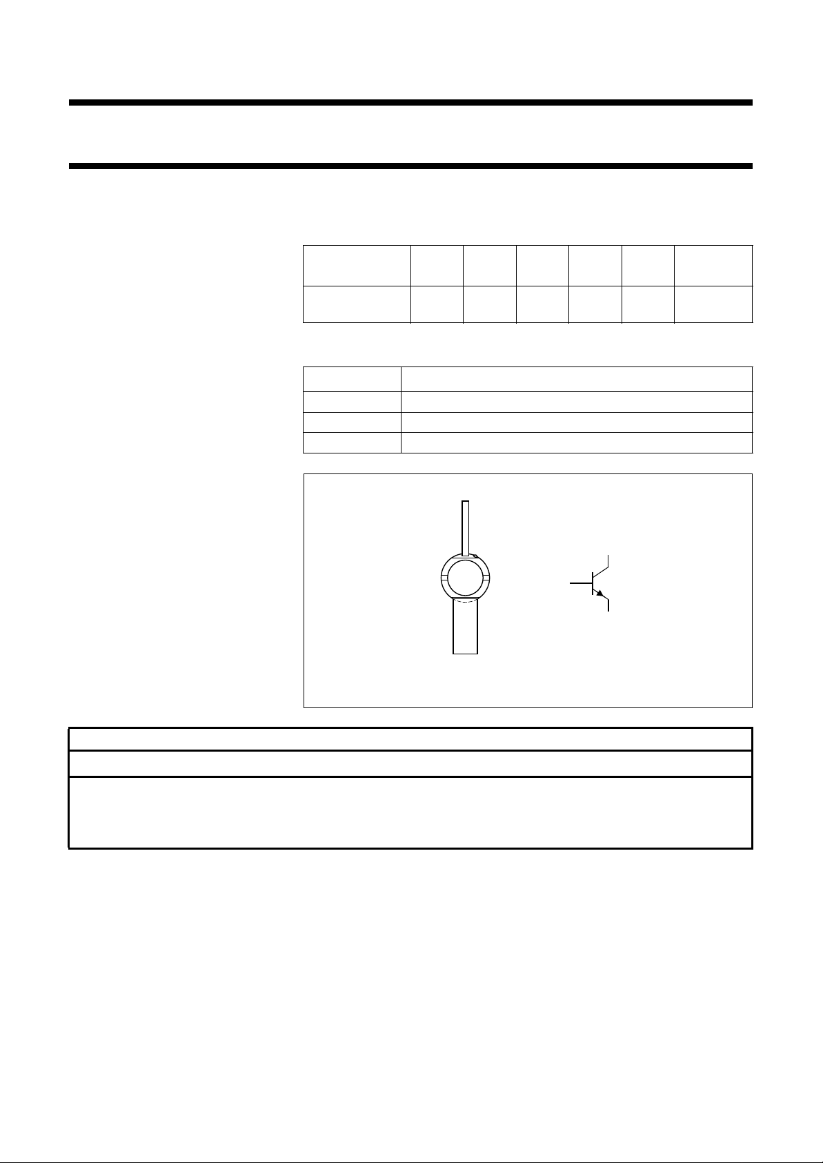
PINNING - SOT446A
PIN DESCRIPTION
1 collector
2 base
3 emitter connected to flange
handbook, halfpage
1
c
3
2
MAM313
b
e
L
Fig.1 Simplified outline and symbol.
WARNING
Product and environmental safety - toxic materials
This product contains beryllium oxide. The product is entirely safe provided that the BeO disc is not damaged.
All persons who handle, use or dispose of this product should be aware of its nature and of the necessary safety
precautions. After use, dispose of as chemical or special waste according to the regulations applying at the location of
the user. It must never be thrown out with the general or domestic waste.
1997 Feb 19 2
Philips Semiconductors Product specification
NPN microwave power transistor LWE2010S
LIMITING VALUES
In accordance with the Absolute Maximum Rating System (IEC 134).
SYMBOL PARAMETER CONDITIONS MIN. MAX. UNIT
V
CBO
V
CER
V
CEO
V
EBO
I
C
P
tot
T
stg
T
j
T
sld
Note
1. Up to 0.1 mm from ceramic.
collector-base voltage open emitter − 40 V
collector-emitter voltage RBE= 250 Ω−20 V
collector-emitter voltage open base − 15 V
emitter-base voltage open collector − 3V
collector current (DC) − 250 mA
total power dissipation Tmb=75°C − 4.8 W
storage temperature −65 +200 °C
operating junction temperature − 200 °C
soldering temperature t ≤ 10 s; note 1 − 235 °C
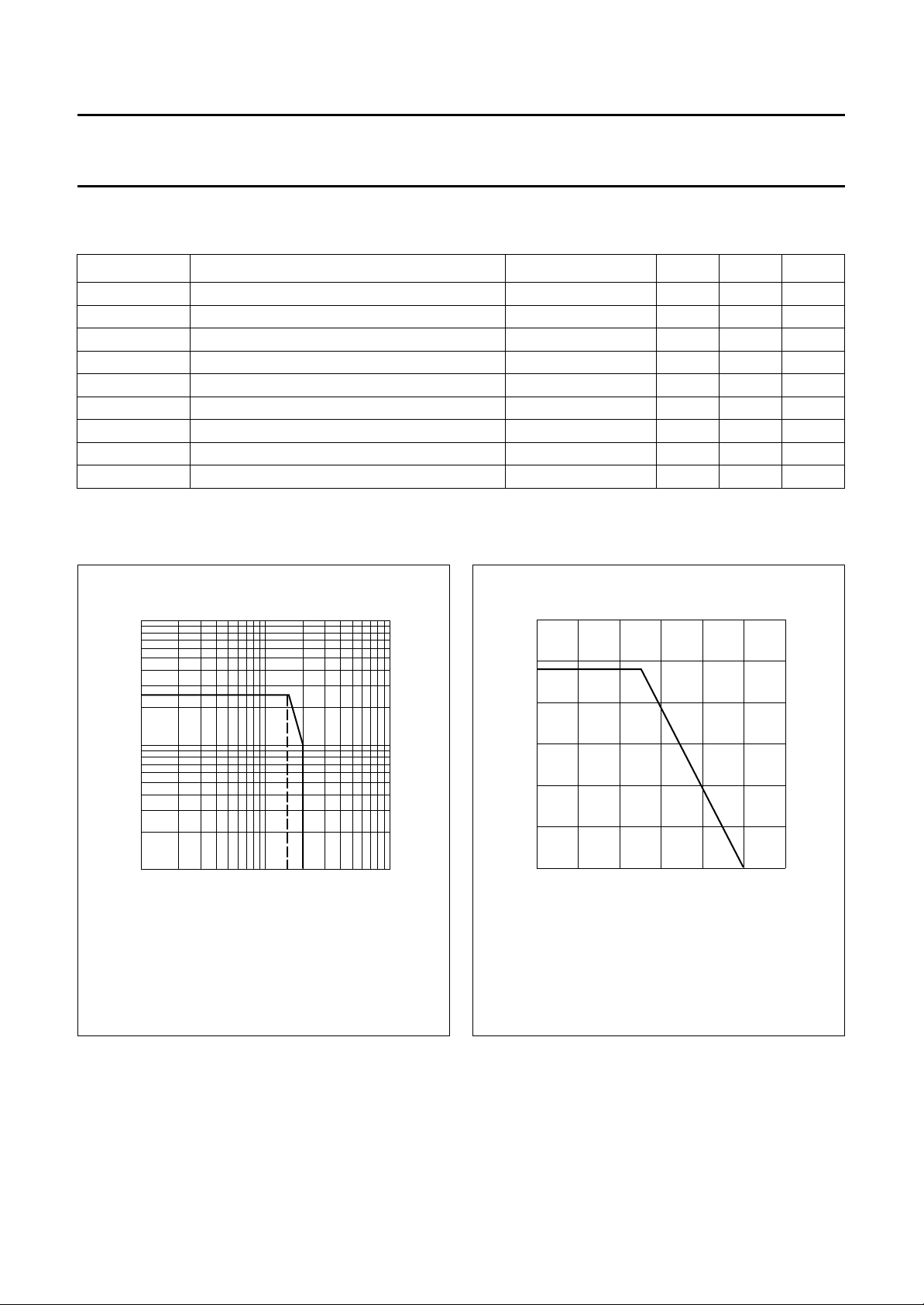
handbook, halfpage
1
I
C
(A)
−1
10
(1)
−2
10
1
Tmb≤ 75°C.
(1) Region of permissible DC operation.
(2) Permissible extension provided RBE≤ 250 Ω.
(2)
10
Fig.2 DC SOAR.
VCE (V)
MGA250
handbook, halfpage
2
10
6
P
tot
(W)
4
2
0
−50 50
P
= 4.8 W.
tot max
150
MGA249
Tmb (
2500 100 200
o
C)
Fig.3 Maximum power dissipation derating as a
function of mounting base temperature.
1997 Feb 19 3

Philips Semiconductors Product specification
NPN microwave power transistor LWE2010S
THERMAL CHARACTERISTICS
SYMBOL PARAMETER CONDITIONS MAX. UNIT
R
th j-mb
R
th mb-h
Note
1. See “
CHARACTERISTICS
=25°C unless otherwise specified.
T
mb
SYMBOL P ARAMETER CONDITIONS MIN. MAX. UNIT
I
CBO
I
EBO
h
FE
thermal resistance from junction to mounting base Tj=75°C 22 K/W
thermal resistance from mounting base to heatsink note 1 2 K/W
Mounting recommendations in the General part of handbook SC15”
.
collector cut-off current VCB=20V; IE=0 − 75 µA
=40V; IE=0 − 500 µA
V
CB
emitter cut-off current VEB= 1.5 V; IC=0 − 200 nA
DC current gain VCE=5V; IC= 110 mA 15 150
APPLICATION INFORMATION
Microwave performance up to T
MODE OF OPERATION
=25°C in a common emitter class A selective amplifier.
mb
f
(GHz)
V
(V)
CE
I
C
(mA)
P
(W)
Class A (CW); note 1 2.3 18 110 ≥0.8;
typ. 0.9
Note
1. In narrowband test circuit shown in Fig.4.
L1
G
po
(dB)
≥8;
typ. 9
Z
(Ω)
I
Z
(Ω)
L
5.2 + j 16.5 7.5 + j 8.75
1997 Feb 19 4
 Loading...