

Philips LVT22V10-DN, LVT22V10-DD, LVT22V10-DA, LVT22V10-BN, LVT22V10-BD Datasheet
...
LVT22V10
3V high speed, universal PLD device
Product specification
Supersedes data of 1996 Mar 12
IC13 Data Handbook
1998 Feb 10
INTEGRATED CIRCUITS
Philips Semiconductors Product specification
LVT22V103V high speed, universal PLD device
2
1998 Feb 10 853-1759 18947
FEA TURES
•Fastest 3V PLD
•Supports 3/5V mixed systems
•Low ground bounce (<1.1V worst case)
•Live insertion/extraction permitted
•Bus-hold data inputs eliminate the need for external pull-up
resistors to hold unused inputs
•Metastable hardened device
•High output drive capability: 32mA/–16mA
•Varied product term distribution with up to 16 product terms per
output for complex functions
•Programmable output polarity
•Available in 300 mil-wide 24-pin Plastic Small Outline Package
•Design support provided for third party CAD development and
programming hardware
DESCRIPTION
The LVT22V10 is a versatile PAL device fabricated on the Philips
BiCMOS QUBiC process.
The QUBiC process produces very high speed 3V devices (7.5ns)
which have excellent noise characteristics. Ground bounce of an
output held low while the remaining 9 outputs switch from high to
low is typically less than 0.7V. V
CC
bounce of an output held high
while the remaining 9 outputs switch from low to high is typically less
than 1.0V .
The LVT22V10 was designed to support mixed 3/5V systems. The
inputs are capable of handling 7V while the outputs can be pulled up
to 7V .
The designer can interface directly from 5V outputs (CMOS full rail
or totem pole) to a 3V LVT input. A 3V LVT output can drive a 5V
TTL input directly , or in the case of a CMOS input, the LVT output
can interface with the use of an external pull-up resistor. Finally, no
external pull-up resistors are needed on unused input pins due to a
bus-hold data structure designed into the LVT input.
The LVT22V10 has been designed with high drive outputs (32mA
sink and 16mA source currents), which allows for direct connection
to a backplane bus. This feature eliminates the need for additional,
standalone bus drivers, which are traditionally required to boost the
drive of a standard PLDs.
The LVT22V10 outputs are designed to support Live
Insertion/Extraction into powered up systems. The output is
specially designed so that during V
CC
ramp, the output remains
3-Stated until V
CC
2.1V . At that time the outputs become fully
functional depending upon device inputs. (See DC Electrical
Characteristics, Symbol I
PU/PD,
Page 5). In addition when an
LVT22V10 output is tied to a 5V bus, no bus current is loaded.
The LVT22V10 uses the familiar AND/OR logic array structure,
which allows direct implementation of sum-of-products equations.
This device has a programmable AND array which drives a fixed OR
array. The OR sum of products feeds an “Output Macro Cell” (OMC)
which can be individually configured as a dedicated input, a
combinatorial output, or a registered output with internal feedback.
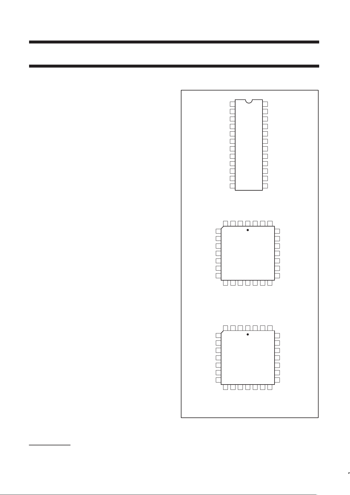
PIN CONFIGURATIONS
1234
5
6
7
8
9
10
11
12 13 14 15 16 17
18
19
20
21
22
23
24
25
262728
1
2
3
4
5
6
7
8
9
10
11
12 13
14
15
16
17
18
19
20
21
22
23
24
D and N Packages
I0/CLK
I1
I2
I3
I4
I5
I6
I7
I8
I9
I10
V
CC
F9
F8
F7
F6
F5
F4
F3
F2
F1
F0
I11
GND
NC
NC
A Package (standard)
NC
CLK/
I0
I1I2
I3
I4
I5
GND
I6
I8
I9 I10
GND
I11 F0 F1
F2
F3
F7
F6
F5
F4
F8F9V
CC
A = Plastic Leaded Chip Carrier
N = Plastic Dual In-Line Package (300mil-wide)
D = Plastic Small Outline Large (300mil-wide) Package
SP00436
NC
1234
5
6
7
8
9
10
11
12 13 14 15 16 17
18
19
20
21
22
23
24
25
262728
A Package (evolutionary)
CLK/
I0
I1I2
I3
I4
I5
I6
I8
I9 I10
GND
I11 F0 F1
F2
F3
F7
F6
F5
F4
F8F9V
CC
A = Plastic Leaded Chip Carrier
GND
V
CC
GND
GND
I7
PAL is a registered trademark of Advanced Micro Devices, Inc.

Philips Semiconductors Product specification
LVT22V10
3V high speed, universal PLD device
1998 Feb 10
3
ORDERING INFORMATION
PACKAGES ORDER CODE DWG NUMBER
24-Pin Plastic DIP (300mil) LVT22V10-7N (8.0ns device) SOT222-1
28-Pin PLCC (standard pinout) LVT22V10B7A (7.5ns device) SOT261-3
28-Pin PLCC (evolutionary pinout) LVT22V10-7A (7.5ns device) SOT261-3
24-Pin Plastic SOL LVT22V10-7D (8.0ns device) SOT137-1
PIN LABEL DESCRIPTIONS
SYMBOL DESCRIPTION
I1 – I11 Dedicated Input
F0 – F9 Macro Cell Input/Output
CLK/I0 Clock Input/Dedicated Input
V
CC
Supply Voltage
GND Ground
NC No Connection
THERMAL RATINGS
TEMPERATURE
Maximum junction 150°C
Maximum ambient 75°C
Allowable thermal rise ambient to junction 75°C
OPERATING RANGES
RATINGS
SYMBOL
PARAMETER
MIN MAX
UNIT
V
CC
Supply voltage +3.0 +3.6 V
DC
T
amb
Operating free-air
temperature
0 +75 °C
ABSOLUTE MAXIMUM RATINGS
1
RATINGS
SYMBOL
PARAMETER
MIN MAX
UNIT
V
CC
Supply voltage
2
–0.5 +4.6 V
DC
V
IN
Input voltage
2
–0.5 7 V
DC
V
OUT
Output voltage
3
–0.5 5.5 V
DC
I
IN
Input currents –30 +30 mA
I
OUT
Output currents +100 mA
T
stg
Storage temperature range –65 +150 °C
NOTES:
1. Stresses above those listed may cause malfunction or permanent damage to the device. This is a stress rating only. Functional operation at
these or any other condition above those indicated in the operational and programming specification of the device is not implied.
2. Except in programming mode.
3. Outputs can be pulled up to 7V via external pull-up resistor.
Philips Semiconductors Product specification
LVT22V10
3V high speed, universal PLD device
1998 Feb 10
4
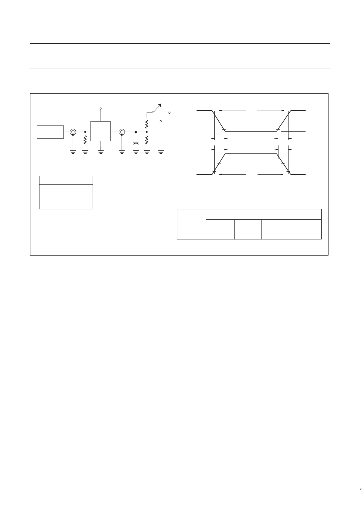
TEST CIRCUIT AND WAVEFORMS
V
M
V
M
t
W
AMP (V)
NEGATIVE
PULSE
10% 10%
90%
90%
0V
V
M
V
M
t
W
AMP (V)
POSITIVE
PULSE
90% 90%
10%
10%
0V
t
THL
(tF)
t
TLH
(tR)t
THL
(tF)
t
TLH
(tR)
VM = 1.5V
DEFINITIONS
R
L
=Load resistor; see AC CHARACTERISTICS for value.
C
L
= Load capacitance includes jig and probe capacitance;
see AC CHARACTERISTICS for value.
R
T
=Termination resistance should be equal to Z
OUT
of pulse
generators.
INPUT PULSE REQUIREMENTS
FAMILY
LVT
PULSE
GENERATOR
V
IN
D.U.T.
V
OUT
C
L
V
CC
R
L
Test Circuit for 3-State Outputs
6.0V
R
T
R
L
OPEN
GND
SWITCH POSITION
TEST SWITCH
t
PLH/tPHL
Open
t
PLZ/tPZL
6V
t
PHZ/tPZH
GND
SP00385
Input Pulse Definition
Amplitude Rep. Rate t
W
t
R
t
F
3.0V 10MHz 500ns 2.5ns 2.5ns
Philips Semiconductors Product specification
LVT22V10
3V high speed, universal PLD device
1998 Feb 10
5
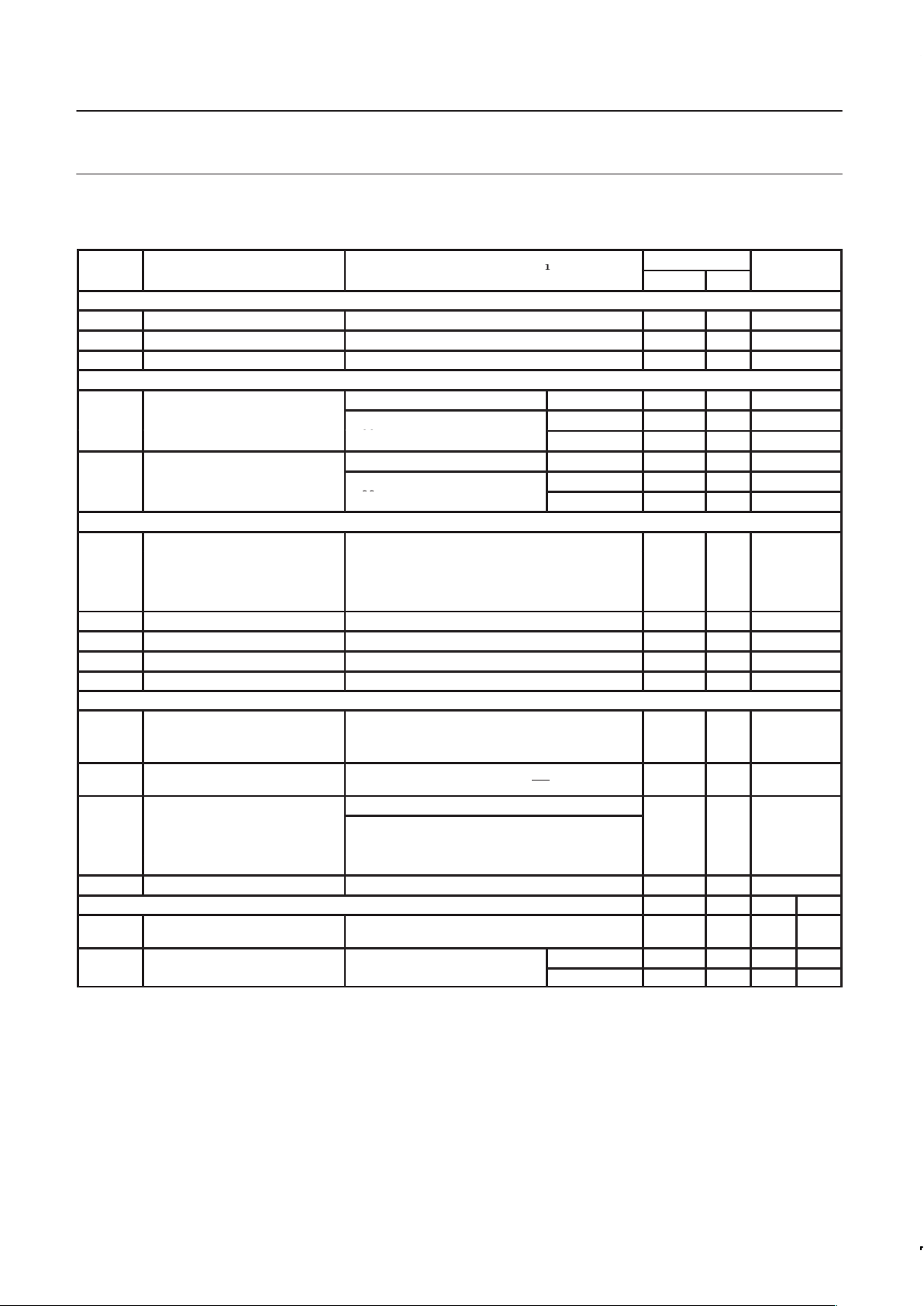
DC ELECTRICAL CHARACTERISTICS
Over operating ranges.
LIMITS
SYMBOL
PARAMETER
TEST CONDITIONS
1
MIN MAX
UNIT
Input voltage
V
IL
Low VCC = MIN 0.8 V
V
IH
High VCC = MAX 2.0 V
V
I
Clamp VCC = MIN, IIN = –18mA –1.2 V
Output voltage
VCC = MIN to MAX, VI = V
IH
or VILIOH = –100 µA VCC–0.2 V
V
OH
High-level output voltage
IOH = –16mA 2.0 V
V
CC
=
MIN, V
I
=
V
IH
or
V
IL
IOH = –5.5 mA 2.4 V
VCC = MIN to MAX, VI = VIH or VILIOL = 100µA 0.2 V
V
OL
Low-level output voltage
IOL = 32 mA 0.5 V
V
CC
=
MIN, V
I
=
V
IH
or
V
IL
IOL = 16 mA 0.4 V
Input current
I
IL
Low VCC = MAX, VIN = 0.0V –10 µA
I
IH
High VCC = MAX, VIN = V
CC
10 µA
I
I
Max input current VCC = MAX, VIN = 5.5V 10 µA
I
I
Pin 1 (program) VCC = MAX, VIN = 5.5V 20 µA
I
BHL
Bus hold low sustaining current
2
VCC = 3V, VI = 0.8V 75 µA
I
BHH
Bus hold high sustaining current
3
VCC = 3V, VI = 2V –75 µA
I
BHLO
Bus hold low overdrive current
4, 9
VCC = 3.6V 500 µA
I
BHHO
Bus hold high overdrive current
5, 9
VCC = 3.6V –500 µA
Output current
I
OFF
Output off current VCC = 0V, VI or VO = 0 to 4.5V ±10 µA
I
EX
Current into an output in high state
when VO > V
CC
VO = 5.5V, VCC = 3.0V ±100 µA
I
PU/PD
Power-up/down 3-State output
current
8
VCC <1.2V; VO = 0.5V to VCC;
VI = GND or VCC; OE/OE = X
100 µA
VCC = MAX
I
OZH
Output leakage
6
VIN = VIL or VIH, V
OUT
= 5.5V 10 µA
I
OZL
Output leakage
6
VIN = VIL or VIH, V
OUT
=0V –10 µA
I
SC
Short circuit
7
V
OUT
= 0.5V –30 –220 mA
I
CC
VCC supply current VCC = 3.6V, Outputs enabled, VI = VCC or GND; IO = 0 170 mA
Ground/VCC Bounce MIN TYP MAX UNIT
V
OHV
Maximum dynamic V
OH
VCC = 3.0V , 25°C,
CL = 50pF (including jig capacitance)
2.2 2.3 V
VCC = 3.3V , 25°C, CL = 50pF
LVT22V10-7 0.7 1.1 V
V
OLP
Maximum dynamic V
OL
CC
, ,
L
(including jig capacitance)
LVT22V10B7 1.0 1.1 V
NOTES:
1. These are absolute values with respect to device ground and all overshoots due to system or tester noise are included.
2. The bus hold circuit can sink at least the minimum low sustaining current at V
IL
MAX. I
BHL
should be measured after lowering VIN to GND
and then raising it to V
IL
MAX.
3. The bus hold circuit can source at least the minimum high sustaining current at V
IH
MIN. I
BHL
should be measured after raising VIN to V
CC
and then lowering it to V
IH MIN.
4. An external driver must source at least I
BHLO
to switch this node from low to high.
5. An external driver must sink at least I
BHHO
to switch this node from high to low.
6. I/O pin leakage is the worst case of I
OZX
or IIX (where X = H or L).
7. No more than one output should be tested at a time. Duration of the short-circuit test should not exceed one second. V
OUT
= 0.5V has been
chosen to avoid test problems caused by tester ground degradation.
8. This parameter is valid for any V
CC
between 0V and 1.2 V with a transition time up to 10 mS. From VCC = 1.2 to VCC = 3.3V ±0.3V a
transition time of 100 µS is permitted. X = Don’t care.
9. These parameters are not 100% tested, but are evaluated at initial characterization and at any time the design is modified where input
current may be affected.

Philips Semiconductors Product specification
LVT22V10
3V high speed, universal PLD device
1998 Feb 10
6
AC ELECTRICAL CHARACTERISTICS
Over commercial operating temperature range.
LIMITS
SYMBOL
PARAMETER
TEST CONDITIONS
1
MIN TYP MAX
UNIT
Input or feedback to non-registered output
2
Active-LOW 7.5 ns
g
PLCC package
Active-HIGH 7.5 ns
t
PD
Input or feedback to non-registered output
2
Active-LOW 8.0 ns
g
DIP and SOL packages
Active-HIGH 8.0 ns
t
S
Setup time from input, feedback or SP to Clock 5.5 ns
t
H
Hold time 0 ns
t
CO
Clock to output 5.0 ns
t
CF
Clock to feedback
3
3.0 ns
t
AR
Asynchronous Reset to registered output 12.0 ns
t
ARW
Asynchronous Reset width 5.0 ns
t
ARR
Asynchronous Reset recovery time 5.0 ns
t
SPR
Synchronous Preset recovery time 5.0 ns
t
WL
Width of Clock LOW 3.0 ns
t
WH
Width of Clock HIGH 3.0 ns
Maximum frequency;
External feedback 1/(tS + tCO)
4
95 MHz
f
MAX
Maximum frequency;
Internal feedback 1/(tS + tCF)
4
118 MHz
t
EA
Input to Output Enable
5
8.5 ns
t
ER
Input to Output Disable
5
8.5 ns
Capacitance
6
Input Capacitance (Pin 1) VIN = 2.0V
=
6 pF
C
IN
Input Capacitance (Others) VIN = 2.0V
V
CC
= 3.3V,
T
amb
= 25°C,
6 pF
C
OUT
Output Capacitance V
OUT
= 2.0V
f = 1MHz
8 pF
NOTES:
1. Test Conditions: R
1
= 500Ω, R2 =500Ω
2. t
PD
is tested with switch S1 open and CL = 50pF (including jig capacitance). VIH = 3V, VIL = 0V, VT = 1.5V .
3. Calculated from measured f
MAX
internal.
4. These parameters are not 100% tested, but are calculated at initial characterization and at any time the design is modified where frequency
may be affected.
5. For 3-State output; output enable times are tested with CL = 50pF to the 1.5V level, and S1 is open for high-impedance to High tests and
closed for high-impedance to Low tests. Output disable times are tested with C
L
= 5pF. High-to-High impedance tests are made to an output
voltage of V
T
= (VOH – 0.3V) with S1 open, and Low-to-High impedance tests are made to the VT = (VOL + 0.3V) level with S1 closed.
6. These parameters are not 100% tested, but are evaluated at initial characterization and at any time the design is modified where
capacitance may be affected.
 Loading...