

Page 1
Philips LPC3000 Evaluation Board Users Manual
Revision History
Revision Date Author Comments A.11 Aug. 6, 2006 Chun Sing Chu
Mike Quirk
© 2005-06 by NOHAU
All Rights Reserved
1
Edit Pass 5 Release
Page 2

Table of Contents
Introduction..................................................................................................................................... 6
EVB Feature List ........................................................................................................................ 6
EVB Configuration .........................................................................................................................
System/RTC Oscillator Selection ...............................................................................................
System Oscillator Selection Jumpers (JP1, JP2)..................................................................... 9
RTC Oscillator...................................................................................................................... 10
Power Supply Configuration..................................................................................................... 10
Power Supply Input Connector (J17).................................................................................... 10
Power Supply Configuration Jumpers .................................................................................. 11
LCD Voltage Regulator (U20).............................................................................................. 13
LCD Contrast Adjustment (R86).....................................................................................................................13
Power Status LED (D2) ........................................................................................................ 13
JTAG/ETB Connector (J18) ..................................................................................................... 14
Reset Switch (S1)...................................................................................................................... 15
Boot Select Input Configuration Jumper (JP32)....................................................................... 16
RS232 Configuration ................................................................................................................ 17
UART 2 Configuration Jumpers (JP2, JP3, JP4, JP5) .......................................................... 17
UART 1/7 Configuration Jumpers (JP12, JP13, JP10, JP11)............................................... 18
UART 5 Configuration Jumpers (JP6, JP7, JP8, JP9) .......................................................... 19
SD Card Connector (J15).......................................................................................................... 20
USB Connectors (J9, J13, J14) ................................................................................................. 20
I2C Bus Address Configuration Jumpers (JP1).................................................................... 20
LCD Module (J19).................................................................................................................... 21
I2C Bus Configuration Jumpers (JP30, JP31) ...................................................................... 21
Contrast Adjustment (R86)................................................................................................... 21
NAND FLASH Chip Select...................................................................................................... 21
NAND FLASH Configuration Jumpers.................................................................................... 22
NAND FLASH Write Protect Input Configuration Jumper (JP29)...................................... 22
NAND FLASH Lock Mechanism & Power-On Auto-Read Configuration Jumper (JP28). 23
ADC Configuration Jumper......................................................................................................
ADC Configuration Jumper (JP33) ...................................................................................... 23
Potentiometer (R83)..............................................................................................................
User Input Push Button Switches .............................................................................................
User Input Push Button Switch (S2)..................................................................................... 24
User Input Push Button Switch (S3)..................................................................................... 24
User Input Push Button Switch (S4)..................................................................................... 24
User Input Push Button Switch (S5).....................................................................................
User Output LEDs..................................................................................................................... 24
User Output LED (D3)..........................................................................................................
User Output LED (D4).......................................................................................................... 25
Default Jumpers Summary Table.................................................................................................. 26
EVB (CPU Board) Default Jumpers Summary Table ..............................................................
EVB (Main Board) Default Jumpers Summary Table..............................................................
Break-Out Headers........................................................................................................................
Break-Out Header (J5)..............................................................................................................
Break-Out Header (J6)..............................................................................................................
Break-Out Header (J7).............................................................................................................. 31
7
9
23
24
24
24
24
26
26
28
29
30
2
Page 3

5. Seehau Configuration................................................................................................................ 33
Installing from the CD .............................................................................................................. 33
Download / Install from Internet............................................................................................... 33
5. Seehau Configuration Program.............................................................................................
Hardware Configuration Tab ....................................................................................................
Configuring the Emulator Options From Within Seehau ......................................................... 39
Map Config TAB ...................................................................................................................... 41
6. NAND Flash Programming ...................................................................................................... 42
NAND Flash Programming Main Dialog Box .........................................................................
NAND Flash Image Options Dialog Box .................................................................................
NAND Flash Erase ................................................................................................................... 46
35
37
42
44
3
Page 4

Index of Figures and Tables
Figure 2-1 EVB (CPU Board) Functional Blocks .......................................................................... 7
Figure 2-2 EVB (Main Board) Functional Blocks.......................................................................... 8
Figure 2-1 EVB (CPU Board) Functional Blocks .......................................................................... 8
Figure 2-3 System Oscillator Selection ..........................................................................................
Figure 2-3 System Oscillator Selection ..........................................................................................
Table 2-1 System Oscillator Selection Jumpers ............................................................................. 9
Table 2-1 System Oscillator Selection Jumpers ............................................................................. 9
Figure 2-4 RTC Oscillator ............................................................................................................ 10
Figure 2-4 RTC Oscillator ............................................................................................................
Figure 2-5 2.0mm Power Connector.............................................................................................
Figure 2-5 2.0mm Power Connector............................................................................................. 10
Table 2-2 1.8V Voltage Regulator Configuration Jumper............................................................ 11
Table 2-2 1.8V Voltage Regulator Configuration Jumper............................................................ 11
Table 2-3 3.0V Voltage Regulator Configuration Jumper............................................................ 11
Table 2-3 3.0V Voltage Regulator Configuration Jumper............................................................ 11
Table 2-4 1.2V Voltage Regulator Configuration Jumper............................................................ 12
Table 2-4 1.2V Voltage Regulator Configuration Jumper............................................................ 12
Table 2-5 0.9V~1.2V Core Voltage Regulator Configuration Jumpers ....................................... 12
Table 2-5 0.9V~1.2V Core Voltage Regulator Configuration Jumpers ....................................... 12
Table 2-6 1.2V RTC Voltage Regulator Configuration Jumpers ................................................. 13
Table 2-6 1.2V RTC Voltage Regulator Configuration Jumpers ................................................. 13
Figure 2-6 JTAG/ETB Connector................................................................................................. 14
Figure 2-6 JTAG/ETB Connector................................................................................................. 14
Figure 2-7 Reset buffering Scheme .............................................................................................. 15
Figure 2-7 Reset buffering Scheme .............................................................................................. 15
Table 2-7 Boot Select Input Configuration Jumper...................................................................... 16
Table 2-7 Boot Select Input Configuration Jumper...................................................................... 16
Table 2-8 UART 2 Configuration Jumpers .................................................................................. 17
Table 2-8 UART 2 Configuration Jumpers ..................................................................................
Table 2-9 UART 1/7 Configuration Jumpers ............................................................................... 18
Table 2-9 UART 1/7 Configuration Jumpers ...............................................................................
Table 2-10 UART 5 Configuration Jumpers ................................................................................
Table 2-10 UART 5 Configuration Jumpers ................................................................................ 19
Table 2-11 I2C Bus Address Configuration Jumper..................................................................... 20
Table 2-11 I2C Bus Address Configuration Jumper..................................................................... 20
Table 2-12 I2C Bus Configuration Jumpers .................................................................................
Table 2-12 I2C Bus Configuration Jumpers ................................................................................. 21
Figure 2-8 NAND FLASH Chip Select........................................................................................
Figure 2-8 NAND FLASH Chip Select........................................................................................ 21
Figure 2-9 SRAM Chip Select...................................................................................................... 22
Figure 2-9 SRAM Chip Select......................................................................................................
Table 2-13 NAND FLASH Write Protect Input Configuration Jumper.......................................
Table 2-13 NAND FLASH Write Protect Input Configuration Jumper.......................................
Table 2-14 NAND FLASH Lock Mechanism & Power-On Auto-Read Configuration Jumper
(JP28) .................................................................................................................................... 23
9
9
10
10
17
18
19
21
21
22
22
22
4
Page 5

Table 2-14 NAND FLASH Lock Mechanism & Power-On Auto-Read Configuration Jumper
(JP28) .................................................................................................................................... 23
Table 2-15 NAND FLASH Lock Mechanism & Power-On Auto-Read Configuration Jumper
(JP28) ....................................................................................................................................
Table 2-15 NAND FLASH Lock Mechanism & Power-On Auto-Read Configuration Jumper
(JP28) ....................................................................................................................................
Table 2-16 ADC Configuration Jumper ....................................................................................... 23
Table 2-16 ADC Configuration Jumper ....................................................................................... 23
Table 2-17 EVB (CPU Board) Default Jumpers Summary Table................................................
Table 2-17 EVB (CPU Board) Default Jumpers Summary Table................................................
Table 2-18 EVB (Main Board) Default Jumpers Summary Table ............................................... 26
Table 2-18 EVB (Main Board) Default Jumpers Summary Table ............................................... 26
Table 2-18 EVB (Main Board) Default Jumpers Summary Table (cont.).................................... 27
Table 2-18 EVB (Main Board) Default Jumpers Summary Table (cont.)....................................
Figure 2-10 Break-Out Header (J5) ..............................................................................................
Figure 2-10 Break-Out Header (J5) .............................................................................................. 29
Figure 2-11 Break-Out Header (J6) .............................................................................................. 30
Figure 2-11 Break-Out Header (J6) .............................................................................................. 30
Figure 2-12 Break-Out Header (J7) .............................................................................................. 31
Figure 2-12 Break-Out Header (J7) .............................................................................................. 31
Break-Out Header (J8).................................................................................................................. 32
Figure 2-13 Break-Out Header (J8) .............................................................................................. 32
Figure 2-13 Break-Out Header (J8) .............................................................................................. 32
Figure 2-14: Emulator Configuration Window Displaying the Connect Tab............................... 35
Figure 2-15: Emulator Configuration Window Displaying the Hdw Config Tab........................ 36
Figure 2-16: JTAG Chain Setup Screen. ...................................................................................... 38
Figure 2-17: Setup Screen with Two Devices .............................................................................. 38
Figure 2-18: Emulator Configuration Window Displaying the Hdw Config Tab........................ 39
Figure 2-19: Emulator Configuration Window Displaying the Misc Setup Tab.......................... 40
Figure 2-20: Emulator Configuration Window Displaying the Map Config Tab ........................ 41
Figure 2-21 NAND Flash Programming Main Dialog .................................................................
Figure 2-22 NAND Flash Image Options..................................................................................... 44
Figure 2-23 NAND Flash Erase Dialog Box ................................................................................
23
23
26
26
27
29
42
46
5
Page 6

1. Introduction
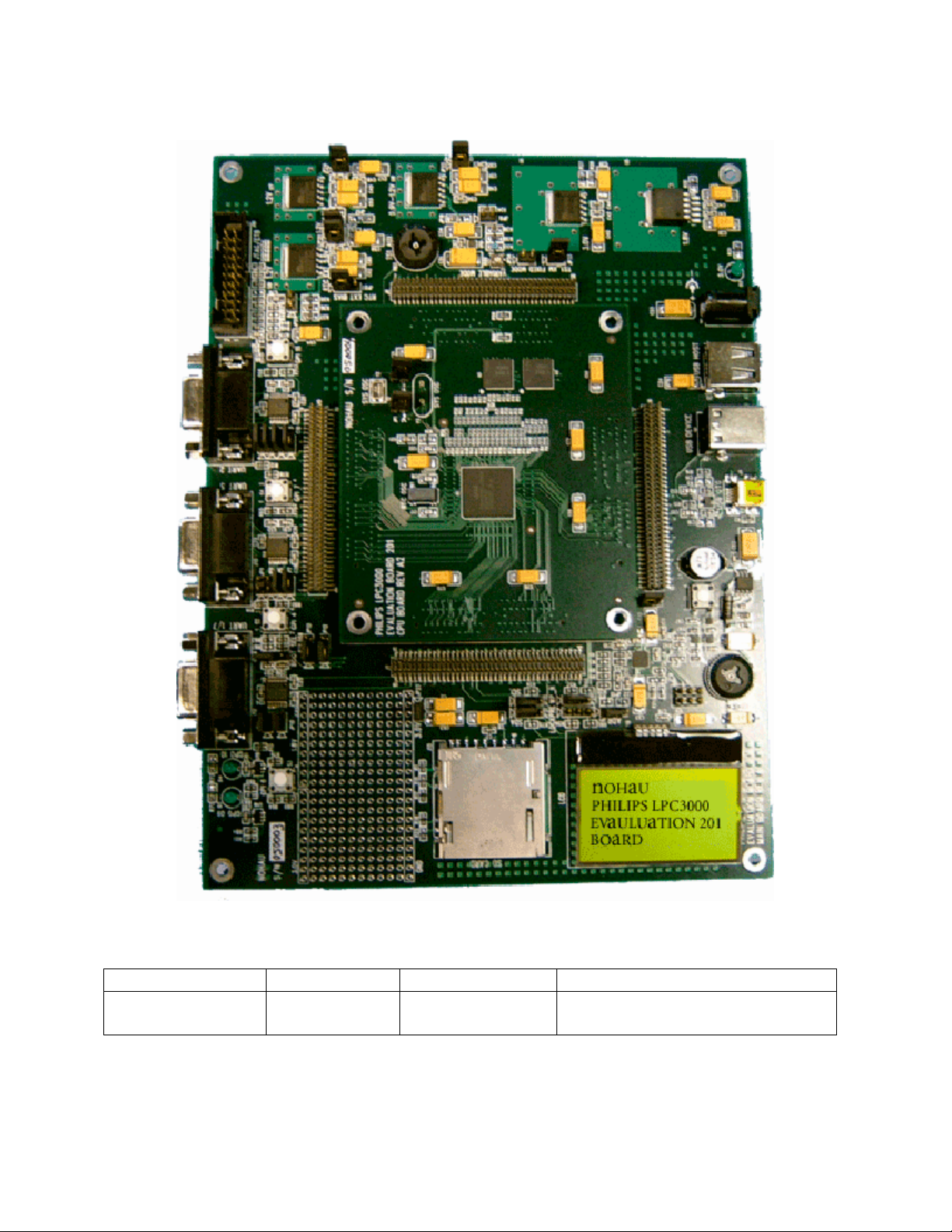
This document details the setup and configuration of the Philips LPC3000 evaluation board 201
(hereafter referred to as the EVB).
The EVB is intended to provide a mechanism for easy customer evaluation of the Philips
LPC3000 microcontroller and to facilitate hardware and software development.
1.1 EVB Feature List
The EVB provides the following features:
- A Single power supply input (5.0V), regulated on board to provide all the necessary EVB
voltages.
- User Reset pushbutton switch.
- 20 Way JTAG/ETB connector.
- 32M (8M x 32) Bytes of SDRAM.
- 32M (32M x 8) Bytes of NAND FLASH.
- 1 - LCD Module with Philips PCF8558 built in.
- 1 - SD Card connector.
- 3 - USB connectors (USB A Receptacle Connector for USB Host; USB B Receptacle
Connector for USB Device; USB Mini AB Receptacle Connector for USB OTG) with
Philips ISP1301.
- 3 - UART (RS232) physical interface circuits connected to standard PC style DB9 female
connectors.
- 4 - 80 pin break-out headers, to provide easy access to many of the microcontroller pins.
- 4 - User input pushbutton switches.
- 2 - User output LEDs.
- Small prototyping area consisting of an area of 0.1 inch spaced through holes with easy
access to ground and 3.0V, 1.8V power supply points.
IMPORTANT
Before you apply power to the EVB, please fully read the following sections on how to
correctly configure the board. However, the boards default configuration should not require
any change in configuration before you power on the EVB.
A Failure in configuration of the board may cause device or EVB damage.
6
Page 7
2. EVB Configuration
This section details the configuration of each of the EVB functional blocks.
Throughout this document, all default jumper settings are clearly marked with “(D)” and are
shown in blue text. This should allow a more rapid return to the default state of the EVB if
required. Note that all 3 pin jumpers have the default configuration with a jumper header fitted to
pins 1-2 except JP28.
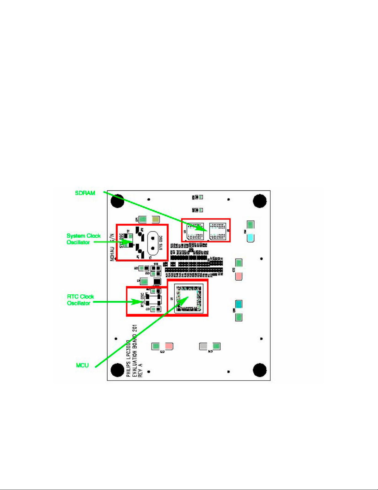
The main EVB functional blocks are shown below to help with quick location of jumpers etc.
The EVB has been designed to try and make it as easy as possible to use. The PCB has detailed
silkscreen legend and, where possible, have been segmented into functional blocks.
Figure 2-1 EVB (CPU Board) Functional Blocks
7
Page 8
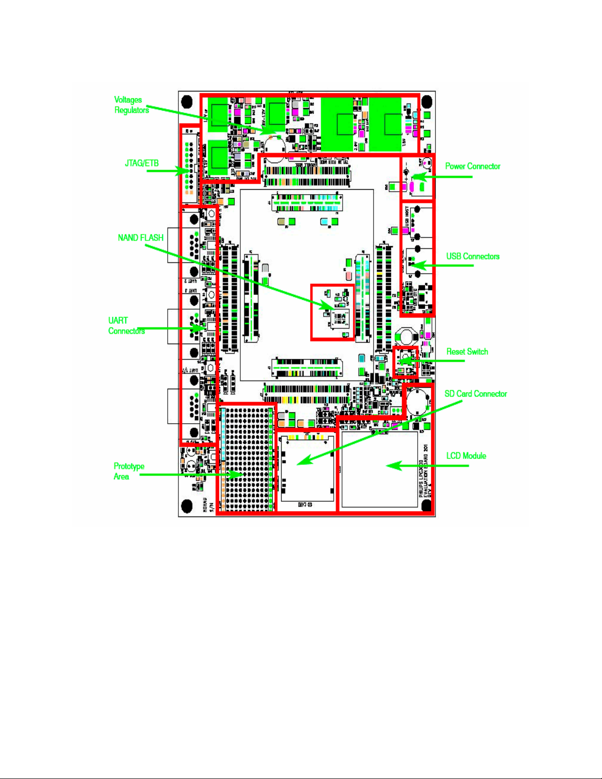
Figure 2-2 EVB (Main Board) Functional Blocks
8
Page 9
2.1 System/RTC Oscillator Selection
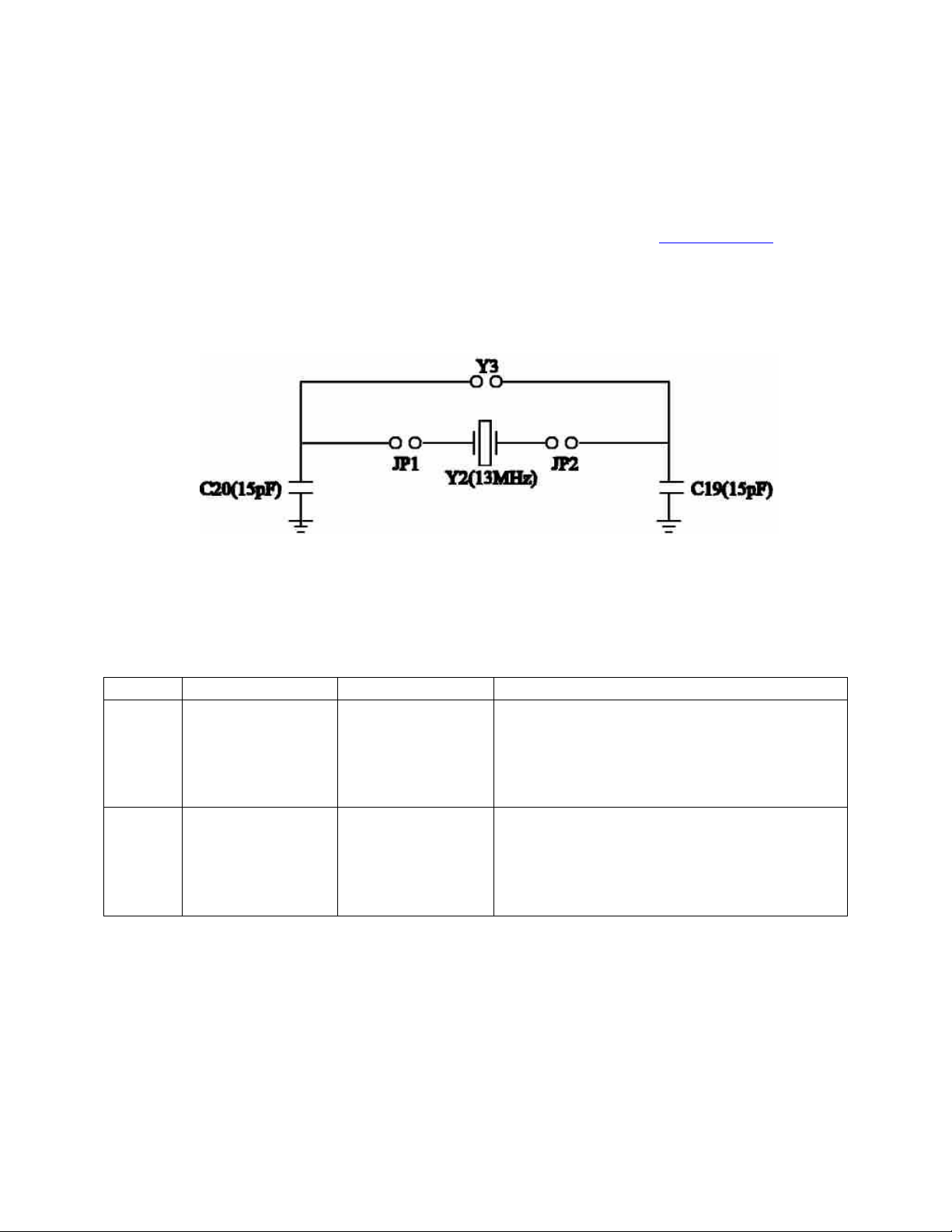
2.1.1 System Oscillator Selection Jumpers (JP1, JP2)
The EVB supports 2 possible MCU system clock oscillator sources:
(1) An on board system clock oscillator Y2 (13MHz).
(2) A socket Y3 for user system clock oscillator.
Appendix figure 1
Figure 2-3 System Oscillator Selection
The selection between these options is controlled using jumpers (JP1, JP2) as shown below:
Table 2-1 System Oscillator Selection Jumpers
Jumper PCB Legend Position Description JP1 FITTED (D)
REMOVED
Connects the on board system clock
oscillator Y2.
Disconnects the on board system clock oscillator. Connects the user system clock oscillator Y3.
JP2 FITTED (D)
REMOVED
Connects the on board system clock
oscillator Y2.
Disconnects the on board system clock oscillator. Connects the user system clock oscillator Y3.
9
Page 10
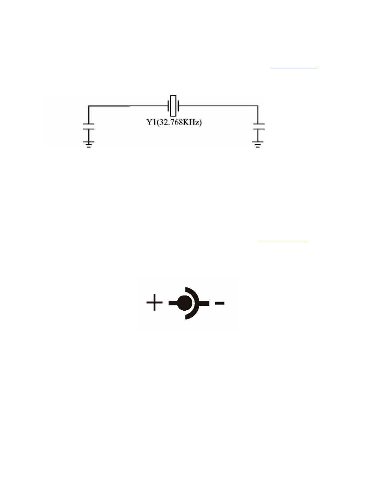
2.1.2 RTC Oscillator
The EVB has a MCU RTC clock oscillator.
Appendix Figure 1
Figure 2-4 RTC Oscillator
2.2 Power Supply Configuration
The EVB requires an external supply voltage of 5V DC, minimum 3Amp.
2.2.1 Power Supply Input Connector (J17)
Appendix Figure 2
This connector provides a convenient hook-up mechanism for a fabricated power lead such as those found on wall-plug DC adapters. Care must be taken to ensure the 2.0mm plug uses the correct polarization as shown below:
Figure 2-5 2.0mm Power Connector
10
Page 11

2.2.2 Power Supply Configuration Jumpers
The EVB has 6 voltage regulators on board:
- 1.8V voltage regulator (U5) to supply the MCU 1.8V voltages (VDDio18, VDDsdram18) and the EVB peripherals 1.8V voltages.
Appendix Figure 2
Table 2-2 1.8V Voltage Regulator Configuration Jumper
Jumper PCB Legend Position Description JP22 1.8V FITTED (D)
REMOVED
- 3.0V voltage regulator (U6) to supply the MCU 3.0V voltages (VDDio28, VDDio1828, VDD1828, VDDad28, VDD28) and the EVB peripherals 3.0V voltages.
Connects the MCU 1.8V voltages and the
EVB peripherals 1.8V voltages.
Allows multimeter to measure the current drawn by the MCU 1.8V voltages.
Appendix Figure 2
Table 2-3 3.0V Voltage Regulator Configuration Jumper
Jumper PCB Legend Position Description JP23 3.0V FITTED (D)
REMOVED
Connects the MCU 3.0V voltages and the
EVB peripherals 3.0V voltages.
Allows multimeter to measure the current drawn by the MCU 3.0V voltages.
- 1.2V voltage regulator (U7) to supply the MCU 1.2V voltages (VDD12, VDDosc12, VDDpll12, VDDcorefixed12).
Appendix Figure 2
11
Page 12

Table 2-4 1.2V Voltage Regulator Configuration Jumper
Jumper PCB Legend Position Description JP24 1.2V FITTED (D)
REMOVED
Connects the MCU 1.2V voltages.
Allows multimeter to measure the current drawn by the MCU 1.2V voltages.
- 0.9V~1.2V core voltage regulator (U8) to supply the MCU 0.9V~1.2V Core voltages (VDDcore12).
Appendix Figure 2
Table 2-5 0.9V~1.2V Core Voltage Regulator Configuration Jumpers
Jumper PCB Legend Position Description JP25 0.9V~1.2V FITTED (D)
REMOVED
Connects the MCU 0.9V~1.2V Core
voltages.
Allows multimeter to measure the current drawn by the MCU 0.9V~1.2V Core voltages.
JP19 REMOVED (D)
FITTED
0.9V~1.2V core voltage regulator output
is set by the signal HIGHCORE.
1.2V for HIGHCORE = LOW;
0.9V for HIGHCORE = HIGH.
0.9V~1.2V core voltage regulator output is set to 0.9V.
JP34 FIXED MODE REMOVED (D)
FITTED
1.2V (for HIGHCORE = LOW) is
configured as 1.17V~1.31V variable mode
controlled by the potentiometer R89.
1.2V (for HIGHCORE = LOW) is configured as 1.17V fixed mode.
12
Page 13

- 1.2V RTC voltage regulator (U9) to supply the MCU 1.2V RTC voltages (VDDrtc12, VDDrtcosc12, VDDrtccore).
Appendix Figure 2
Table 2-6 1.2V RTC Voltage Regulator Configuration Jumpers
Jumper PCB Legend Position Description JP26 1.2V FITTED (D)
REMOVED
Connects the MCU 1.2V RTC voltages.
Allows multimeter to measure the current drawn by the MCU 1.2V RTC voltages.
JP21 REMOVED (D)
FITTED
1.2V RTC voltage regulator output is set
to 1.2V.
1.2V RTC voltage regulator output is set to 0.9V.
JP20 RTC EXT 5.0V FITTED (D)
REMOVED
1.2V RTC voltage regulator input is
connected to the power supply input
connector J17.
1.2V RTC voltage regulator input is disconnected from the power supply input connector J17. 1.2V RTC voltage regulator input can then be connected to external 5.0V power supply through the pin 1 of JP20.
JP27 RTC EXT BIAS 1-2 (D)
2-3
When JP20 is fitted.
When JP20 is removed.
2.2.3 LCD Voltage Regulator (U20)
- 3.3V LCD voltage regulator (U20) to supply the LCD voltage.
2.2.3.1 LCD Contrast Adjustment (R86)
- The Contrast Adjustment for the LCD is controlled by the potentiometer R86.
2.2.4 Power Status LED (D2)
When power is applied to the EVB, the green Power Status LED (D2) adjacent to the Power Supply Input Connector (J17) shows the presence of the 5.0V supply voltage.
Appendix Figure 2
13
Page 14
2.3 JTAG/ETB Connector (J18)
Appendix Figure 3
The JTAG/ETB connector (J18) on the edge of the EVB supports the 20–pin debug interface connector.
About ETB (Embedded Trace Buffer)
As process speeds increase it is increasingly difficult to obtain trace information off a chip from
the Embedded Trace Macrocell (ETM). This causes difficulties in maintaining acceptable signal
quality or the signals need to be demultiplexed on to what can become a very large number of
trace port pins.
The solution is to provide a buffer area on-chip where the trace information is stored, and read from the chip latter, at a slower rate.
The ETB stores data produced by the ETM. The buffered data can then be accessed by the debugging tools using a JTAG (IEEE 1149.1) interface, as shown in figure 2-6.
** Important **
When connecting or removing the JTAG/ETB debug interface,
power must be removed from both the EVB and the
JTAG/ETB debug interface.
Figure 2-6 JTAG/ETB Connector
14
Page 15
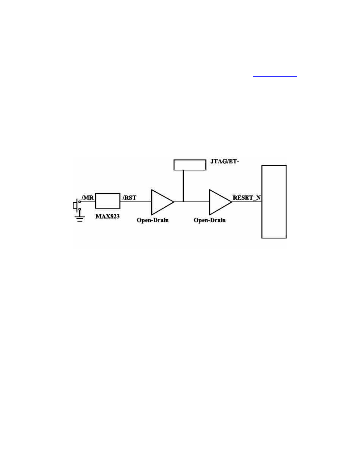
2.4 Reset Switch (S1)
Appendix Figure 3
An active low, push button RESET switch (S1) with a MAXIM MAX823REXK-T device is
provided on the EVB. When the 3.0V voltage regulator drops below a certain threshold level
(2.63V), the MAXIM MAX823REXK-T device will automatically assert the MCU reset line in
order to prevent incorrect operation of the MCU or EVB circuitry. The MAXIM
MAX823REXK-T device also provides a de-bounced input for the active low, push button
RESET switch (S1). As the JTAG hardware debug probe has the ability to assert the MCU reset
line, additional open-drain output buffering scheme is created as shown in Figure 2-7.
Figure 2-7 Reset buffering Scheme
15
Page 16

2.5 Boot Select Input Configuration Jumper (JP32)
Appendix Figure 3
The Boot Select Input, GPI_01 (SERVICE_N) is configured by the jumper (JP32).
Table 2-7 Boot Select Input Configuration Jumper
Jumper PCB Legend Position Description JP32 BOOT SEL 1-2 (D)
2-3
GPI_01(SERVICE_N) is set to HIGH to
run code from NAND FLASH.
GPI_01(SERVICE_N) is set to LOW to download code from UART 5 (J10).
16
Page 17

2.6 RS232 Configuration
The EVB has three MAXIM MAX3232ECAE RS232 transceiver devices, providing RS232
signal translation for the MCU. Each of the MAXIM MAX3232ECAE devices has a 9 way
female D-Type connector associated. Each of the MCU signals to the RS232 transceiver is
jumpered to allow individual isolation if required.
2.6.1 UART 2 Configuration Jumpers (JP2, JP3, JP4, JP5)
Appendix Figure 3
For the UART 2, the MAXIM MAX3232ECAE device (U2) has a 9 way female D-Type connector (J11) associated.
Table 2-8 UART 2 Configuration Jumpers
Jumper PCB Legend Position Description JP2 FITTED (D)
REMOVED
Connects U2_TX to MAXIM
MAX3232ECAE device.
Disconnects U2_TX from MAXIM MAX3232ECAE device.
JP3 FITTED (D)
REMOVED
Connects U2_RX to MAXIM
MAX3232ECAE device.
Disconnects U2_RX from MAXIM MAX3232ECAE device.
JP4 FITTED (D)
REMOVED
Connects U2_HRTS to MAXIM
MAX3232ECAE device.
Disconnects U2_HRTS from MAXIM MAX3232ECAE device.
JP5 FITTED (D)
REMOVED
Connects U2_HCTS to MAXIM
MAX3232ECAE device.
Disconnects U2_HCTS from MAXIM MAX3232ECAE device.
17
Page 18

2.6.2 UART 1/7 Configuration Jumpers (JP12, JP13, JP10, JP11)
Appendix Figure 3
For the UART 1/7, the MAXIM MAX3232ECAE device (U3) has a 9 way female D-Type connector (J12) associated.
Table 2-9 UART 1/7 Configuration Jumpers
Jumper PCB Legend Position Description JP12 1-2 (D)
2-3
Connects U7_TX to MAXIM
MAX3232ECAE device.
Connects U1_TX to MAXIM MAX3232ECAE device.
JP13 1-2 (D)
2-3
Connects U7_RX to MAXIM
MAX3232ECAE device.
Connects U1_RX to MAXIM MAX3232ECAE device.
JP10 FITTED (D)
REMOVED
Connects U7_HRTS to MAXIM
MAX3232ECAE device.
Disconnects U7_HRTS from MAXIM MAX3232ECAE device.
JP11 FITTED (D)
REMOVED
Connects U7_HCTS to MAXIM
MAX3232ECAE device.
Disconnects U7_HCTS from MAXIM MAX3232ECAE device.
18
Page 19

2.6.3 UART 5 Configuration Jumpers (JP6, JP7, JP8, JP9)
Appendix Figure 3
For the UART 5, the MAXIM MAX3232ECAE device (U4) has a 9 way female D-Type connector (J10) associated.
Table 2-10 UART 5 Configuration Jumpers
Jumper PCB Legend Position Description JP6 FITTED (D)
REMOVED
Connects U5_TX to MAXIM
MAX3232ECAE device.
Disconnects U5_TX from MAXIM MAX3232ECAE device.
JP7 FITTED (D)
REMOVED
Connects U5_RX to MAXIM
MAX3232ECAE device.
Disconnects U5_RX from MAXIM
MAX3232ECAE device.
JP8 REMOVED (D) Not in use.
JP9 REMOVED (D) Not in use.
19
Page 20

2.7 SD Card Connector (J15)
Appendix Figure 3
The EVB supports SD Card with a SD Card connector.
The Detect switch of the SD Card connector is connected to the GPI_5 pin of the MCU.
The output of the Detect switch is LOW when the SD Card is inserted.
2.8 USB Connectors (J9, J13, J14)
Appendix Figure 3
The EVB has 3 x USB connectors with a Universal Serial Bus (USB) On-The-Go (OTG) transceiver device, Philips ISP1301.
- USB A Receptacle Connector for USB Host (J13).
- USB B Receptacle Connector for USB Device (J14).
- USB Mini AB Receptacle Connector for USB OTG (J9).
2.8.1 I2C Bus Address Configuration Jumpers (JP1)
Appendix Figure 3
The least least-significant I2C-bus address bit of the Philips ISP1301 is configured by the jumper JP1.
Table 2-11 I2C Bus Address Configuration Jumper
Jumper PCB Legend Position Description JP1 ADR 1-2 (D)
2-3
The I2C-bus address for the Philips
ISP1301 is 0101101 (0x2D).
The I2C-bus address for the Philips
ISP1301 is 0101100 (0x2C).
20
Page 21

2.9 LCD Module (J19)
Appendix Figure 3
The EVB has a LCD module with Philips PCF8558 built in.
2.9.1 I2C Bus Configuration Jumpers (JP30, JP31)
Appendix Figure 3
The I2C bus of the LCD module is configured by the jumpers (JP30, JP31).
Table 2-12 I2C Bus Configuration Jumpers
Jumper PCB Legend Position Description JP30 SCL 1-2 (D)
2-3
JP31 SDA 1-2 (D)
2-3
Connects I2C1_SCL.
Connects I2C2_SCL.
Connects I2C1_SDA.
Connects I2C2_SDA.
2.9.2 Contrast Adjustment (R86)
Appendix Figure 3
The Contrast Adjustment of the LCD module is controlled by the potentiometer R86.
2.10 NAND FLASH Chip Select
The on-board NAND FLASH chip select is re-created as shown in Figure 2-8.
Figure 2-8 NAND FLASH Chip Select
21
Page 22

The SRAM chip select available at the break-out header, is re-created as shown in Figure 2-9.
Figure 2-9 SRAM Chip Select
The normal state of the signal GP0_1 is low after reset from the microcontroller. This means
that the Flash Chip Enable signal will be active. Since there is no actual enable for Static RAM
from the micro we have added a signal ( SRAM_CE ), that the user can enable by setting the
GP0_1 signal to a high state to enable access to Static RAM.
2.11 NAND FLASH Configuration Jumpers
2.11.1 NAND FLASH Write Protect Input Configuration Jumper (JP29)
Appendix Figure 4
Table 2-13 NAND FLASH Write Protect Input Configuration Jumper
Jumper PCB Legend Position Description JP29 WP_N 1-2 (D)
2-3
Accepts program or erase operations.
Does not accept any program or erase
operations.
22
Page 23

2.11.2 NAND FLASH Lock Mechanism & Power-On Auto-Read Configuration Jumper (JP28)
Appendix Figure 4
The table below shows the configuration of the Jumper (JP28) if ST NAND256R3A2AZA6E is installed on the board.
Table 2-14 NAND FLASH Lock Mechanism & Power-On Auto-Read Configuration
Jumper (JP28)
Jumper PCB Legend Position Description JP28 LOCKPRE REMOVED (D) Not using LOCK MECHANISM &
POWER-ON AUTO-READ is not
supported.
The table below shows the configuration of the Jumper (JP28) if SAMSUNG K9F5608Q0CGIB0 is installed on the board.
Table 2-15 NAND FLASH Lock Mechanism & Power-On Auto-Read Configuration
Jumper (JP28)
Jumper PCB Legend Position Description JP28 LOCKPRE 2-3 (D)
1-2
LOCK MECHANISM & POWER-ON
AUTO-READ disabled.
LOCK MECHANISM & POWER-ON
AUTO-READ enabled.
2.12 ADC Configuration Jumper
2.12.1 ADC Configuration Jumper (JP33)
Table 2-16 ADC Configuration Jumper
Jumper PCB Legend Position Description JP33 ADIN1 FITTED (D)
REMOVED
Connects ADIN1 to 0.9V~1.2V Core
voltage.
Disconnects ADIN1 to 0.9V~1.2V Core
Voltage.
23
Appendix Figure 4
Page 24

2.12.2 Potentiometer (R83)
ADIN2 is connected to the 3.0V voltage through the potentiometer R83.
2.13 User Input Push Button Switches
2.13.1 User Input Push Button Switch (S2)
An active low, push button switch (S2) is connected to GPI_4.
2.13.2 User Input Push Button Switch (S3)
An active low, push button switch (S3) is connected to GPI_6.
2.13.3 User Input Push Button Switch (S4)
Appendix Figure 4
Appendix Figure 4
Appendix Figure 4
An active low, push button switch (S3) is connected to GPI_7.
2.13.4 User Input Push Button Switch (S5)
An active low, push button switch (S5) is connected to GPI_11.
2.14 User Output LEDs
2.14.1 User Output LED (D3)
LED (D3) is driven by GPO_9.
Appendix Figure 4
Appendix Figure 4
Appendix Figure 5
24
Page 25

2.14.2 User Output LED (D4)
LED (D4) is driven by GPO_10.
Appendix Figure 5
25
Page 26

3. Default Jumpers Summary Table
3.1 EVB (CPU Board) Default Jumpers Summary Table
Table 2-17 EVB (CPU Board) Default Jumpers Summary Table
Jumper PCB Legend Position Description JP1 FITTED (D)
JP2 FITTED (D)
Connects the on board system clock
oscillator Y2.
Connects the on board system clock
oscillator Y2.
3.2 EVB (Main Board) Default Jumpers Summary Table
Table 2-18 EVB (Main Board) Default Jumpers Summary Table
Jumper PCB Legend Position Description JP22 1.8V FITTED (D)
JP23 3.0V FITTED (D)
JP24 1.2V FITTED (D) Connects the MCU 1.2V voltages.
JP25 0.9V~1.2V FITTED (D)
JP19 REMOVED (D)
JP34 FIXED MODE REMOVED (D)
JP26 1.2V FITTED (D) Connects the MCU 1.2V RTC voltages. JP21 REMOVED (D)
JP20 RTC EXT 5.0V FITTED (D)
JP27 RTC EXT BIAS 1-2 (D) When JP20 is fitted. JP32 BOOT SEL 1-2 (D)
Connects the MCU 1.8V voltages and the
EVB peripherals 1.8V voltages.
Connects the MCU 3.0V voltages and the
EVB peripherals 3.0V voltages.
Connects the MCU 0.9V~1.2V Core
voltages.
0.9V~1.2V core voltage regulator output
is set by the signal HIGHCORE.
1.2V for HIGHCORE = LOW;
0.9V for HIGHCORE = HIGH.
1.2V (for HIGHCORE = LOW) is
configured as 1.17V~1.31V variable mode
controlled by the potentiometer R89.
1.2V RTC voltage regulator output is set
to 1.2V.
1.2V RTC voltage regulator input is
connected to the power supply input
connector J17.
GPI_01(SERVICE_N) is set to HIGH to
run code from NAND FLASH.
26
Page 27

Table 2-18 EVB (Main Board) Default Jumpers Summary Table (cont.)
Jumper PCB Legend Position Description JP2 FITTED (D)
JP3 FITTED (D)
JP4 FITTED (D)
JP5 FITTED (D)
JP12 1-2 (D)
JP13 1-2 (D)
JP10 FITTED (D)
JP11 FITTED (D)
JP6 FITTED (D)
JP7 FITTED (D)
JP8 REMOVED (D) Not in use.
JP9 REMOVED (D) Not in use.
JP1 ADR FITTED (D)
JP30 SCL 1-2 (D) Connects I2C1_SCL.
JP31 SDA 1-2 (D) Connects I2C1_SDA.
JP29 WP_N 1-2 (D) Accepts program or erase operations.
JP28 LOCKPRE REMOVED (D) Not using LOCK MECHANISM &
JP33 ADIN1 FITTED (D)
Connects U2_TX to MAXIM
MAX3232ECAE device.
Connects U2_RX to MAXIM
MAX3232ECAE device.
Connects U2_HRTS to MAXIM
MAX3232ECAE device.
Connects U2_HCTS to MAXIM
MAX3232ECAE device.
Connects U7_TX to MAXIM
MAX3232ECAE device.
Connects U7_RX to MAXIM
MAX3232ECAE device.
Connects U7_HRTS to MAXIM
MAX3232ECAE device.
Connects U7_HCTS to MAXIM
MAX3232ECAE device.
Connects U5_TX to MAXIM
MAX3232ECAE device.
Connects U5_RX to MAXIM
MAX3232ECAE device.
The I2C-bus address for the Philips
ISP1301 is 0101101 (0x2D).
POWER-ON AUTO-READ is not
supported.
Connects ADIN1 to 0.9V~1.2V Core
voltage.
27
Page 28

4. Break-Out Headers
This section details the pinout for the break-out headers on the EVB. All of the break-out headers are all 0.05 inch pitch headers (SAMTEC FTR-140-52-G-D-A).
28
Page 29

4.1 Break-Out Header (J5)
ONSW
GP0_17
GND
GND
GP1_11
U1_TX
U2_TX
U1_R1
GND
U2_HCTS
NC
VDDio1828
NC
NC
U6_IRTX
NC
NC
U5_4X
VDDio1828
U7_HCTS
U5_TX
KEY_COL3
GND
KEY_COL0
KEY_COL4
KEY_ROW5
KEY_COL1
KEY_ROW1
VDDio28
NC
NC
NC
GND
PWM_OUT1
GPI_4
GPI_8
GPO_2
GPI_9
GPO_6
GP0_10
Figure 2-10 Break-Out Header (J5)
80
78
76
74
72
70
68
66
64
62
60
58
56
54
52
50
48
46
44
42
40
38
36
34
32
30
28
26
24
22
20
18
16
14
12
10
Appendix Figure 5
79
77
75
73
71
69
67
65
63
61
59
57
55
53
51
49
47
45
43
41
39
37
35
33
31
29
27
25
23
21
19
17
15
13
11
9
8
6
4
2
7
5
3
1
NC
GPI_5
NC
U2_HRTS
NC
GND
GND
GND
GND
GND
U2_RX
U3_RX
U3_TX
NC
SYSCLKEN
NC
HIGHCORE
U6_IRRX
U7_TX
KEY_COL5
U7_RX
KEY_COL2
TEST
KEY_ROW4
GND
KEY_ROW2
KEY_ROW3
GND
KEY_ROW0
NC
PWM_OUT2
GPI_0
GPI_2
GPI_7
GPI_1
GPI_10
NC
GPO_3
GP0_7
GPO_8
29
Page 30

4.2 Break-Out Header (J6)
VDDio18
FLASH_CLE
FLASH_ALE
FLASH_RD_N
FLASH_IO6
FLASH_RB_N
VDDio18
FLASH_IO2
FLASH_IO3
FLASH_IO0
NC
NC
NC
NC
GND
GND
NC
NC
GND
NC
NC
NC
NC
NC
NC
NC
NC
NC
NC
NC
NC
NC
NC
NC
GND
NC
NC
NC
NC
NC
Figure 2-11 Break-Out Header (J6)
80
78
76
74
72
70
68
66
64
62
60
58
56
54
52
50
48
46
44
42
40
38
36
34
32
30
28
26
24
22
20
18
16
14
12
10
Appendix Figure 5
8
6
4
2
NC
79
NC
77
NC
75
NC
73
NC
71
GND
69
NC
67
NC
65
GND
63
FLASH_WR_N
61
NC
59
FLASH_IO7
57
FLASH_IO4
55
FLASH_IO5
53
NC
51
FLASH_IO1
49
NC
47
NC
45
NC
43
NC
41
NC
39
NC
37
GND
35
NC
33
NC
31
NC
29
GND
27
NC
25
NC
23
SRAM.CD_N
21
NC
19
NC
17
NC
15
NC
13
GND
11
NC
9
NC
7
NC
5
GND
3
NC
1
30
Page 31

4.3 Break-Out Header (J7)
GIO_9
GPO_16
GPI_21
U7_HRTS
GPO_15
GPIO_5
SPI_DATIN
GPIO_4
VDDio28
MS_DIO1
MS_DIO3
SPI2_DATIO
GND
MS_DIO0
I2C1_SCL
MS_DIO2
MS_SCLK
I2C1_SDA
NC
GND
GPI_6
GND
VDD1828
GND
GND
GND
GND
GND
USB_INT_N
VDDio18
USB_DAT_VP
USB_I2C_SCL
I2C2_SDA
GPO_1
GND
GPO_19
GPI_3
GND
NC
GND
Figure 2-12 Break-Out Header (J7)
Appendix Figure 5
80
78
76
74
72
70
68
66
64
62
60
58
56
54
52
50
48
46
44
42
40
38
36
34
32
30
28
26
24
22
20
18
16
14
12
10
8
6
4
2
79
77
75
73
71
69
67
65
63
61
59
57
55
53
51
49
47
45
43
41
39
37
35
33
31
29
27
25
23
21
19
17
15
13
11
9
7
5
3
1
GND
GPO_13
GPO_12
GPO_18
GMD
GPIO_1
GPIO_0
GPIO_3
GPIO_2
NC
SPI2_CLK
SPI1_DATIN
SPI1_CLK
SPI1_DATIO
GPO_4
MS_BS
GPO_11
GND
GND
NC
NC
GND
GND
VDD1828
GND
GND
NC
USB_OE_TP_N
USB_SE0_VM
USB_I2C_SDA
GND
I2C2_SCL
GPO_0
GPO_14
GPO_5
GPO_20
VDDio18
GND
RESOUT_N
NC
31
Page 32

4.4 Break-Out Header (J8)
GND
NC
NC
NC
NC
NC
NC
GND
NC
NC
NC
NC
NC
GND
VDDts28
NC
VDDts28
NC
ADIN2
NC
GND
NC
NC
GND
NC
GND
GND
NC
NC
NC
GND
NC
GND
GND
GND
NC
VDD28
NC
RESET_N
GND
Figure 2-13 Break-Out Header (J8)
Appendix Figure 5
80
78
76
74
72
70
68
66
64
62
60
58
56
54
52
50
48
46
44
42
40
38
36
34
32
30
28
26
24
22
20
18
16
14
12
10
8
6
4
2
79
77
75
73
71
69
67
65
63
61
59
57
55
53
51
49
47
45
43
41
39
37
35
33
31
29
27
25
23
21
19
17
15
13
11
9
7
5
3
1
NC
NC
NC
NC
NC
NC
NC
NC
NC
NC
GND
NC
NC
NC
ADIN1
NC
ADIN0
NC
GND
NC
NC
NC
NC
NC
GND
GND
GND
VDD28
NC
NC
VDD28
VDD28
GND
VDD28
NC
GND
NC
NC
GND
NC
32
Page 33

5. Seehau Configuration
Installing from the CD
To install the Seehau software, do the following:
1. Insert the Seehau CD into your CD ROM drive. The installation process will start
automatically.
2. Click Install Seehau Interface for EMUL-ARM and follow the instructions that appear
on your screen.
If the installation does not start automatically, you might have your Windows Autorun feature
disabled. You will then need to do one of three things:
• Use Windows Explorer and navigate to the CD root directory. Double-click Autorun.exe.
The Windows Install Shield will start the installation process.
• Right-click on the CD ROM symbol while running Windows Explorer and select
AutoPlay to start the installation process.
• From the taskbar, select Start, then Settings. Click on Control Panel, then Add/Remove
Programs, and then Install. The installation process will start when you select the correct
path to the CD.
Downloading and Installing the Seehau Software From the Internet
1. Go to the Nohau web site (http://www.nohau.com). Click Downloads. The Nohau
Software
2. Click Current Seehau Software. The Seehau Software Status page opens.
3. Locate the EMUL–ARM product listing. There will be two listings: one for documentation
and one for software.
4. Click Information and Download (Seehau).
5. Review the information on the page.
6. Click Yes I Want to Download. A Customer Information Form page opens. Complete this
form, then click Proceed. (You have the option to download more than one product.) A
verification page opens with the information you have just entered. If all information is
correct, select SEND at the bottom of the page. A message will open that verifies your
information has been sent.
7. Click Go to Download. The Available Download Areas page opens.
Downloads page opens.
8. Click either option for a download site. The Nohau Software Updates page opens.
9. Click the EMUL–ARM link.
33
Page 34

10. Click the ARM.exe link. The application will start downloading. Make a note of the
directory for this downloaded file.
11. Following the download, go to the directory which has the downloaded file. Click the
ARM.exe file and follow the installation instructions.
After installing the Seehau software, the Setup Complete dialog box appears, allowing you to
view the Readme.txt file and/or launch the SeehauARM configuration.
Note
You must launch the SeehauARM configuration before running the Seehau software.
34
Page 35

Seehau Configuration Program
After installing Seehau, it is recommended that you automatically start the Seehau
Configuration program. Do the following steps before starting Seehau:
1. From the Setup Complete dialog box, select Launch SeehauARM Configuration.
2. Click Finish.
If you do not choose to automatically start the Seehau Configuration Program, do the
following:
From the Start menu, select Programs.
Select SeehauARM. then click Config to open the Emulator Configuration window
displaying the Connect tab (Figure 2-14). Please note that it is not necessary to be connected
at this time.
Figure 2-14: Emulator Configuration Window Displaying the Connect Tab
35
Page 36

Configuring the Communications Interface Connect Tab
The graphical user interface for this tab is divided into four regions:
1. Region 1 – Communications Interface:
Displays the three communications interface options for the ARM. The USB is for the pod
only. If you have the optional Compact Trace Module (CTM), choose the USB-CTM (in
the middle). The third box is for the GigaTrace option.
2. Region 2 – Select Emulator Connection:
No action required. Default is Universal Serial Bus.
3. Region 3 – Select Processor:
Default is ARM7 (generic). Click on the arrow to view the drop down list for the other
devices. For ARM9,
4. Region 4 – What is your Trace Type?:
The default is Yes
select ARM9 (generic).
if trace is supported (based on earlier selections).
5. Click
Next. The Hdw Config tab opens (Figure 2-15).
Figure 2-15: Emulator Configuration Window Displaying the Hdw Config Tab
36
Page 37

Hardware Configuration Tab
The initial configuration settings are read from the Startup.bas file when the debugger
initializes.
After the initial startup and configuration of Seehau, the configuration parameters are saved in
the Startup.bas file (located in the Macro subdirectory). The next time the emulator is started,
the configuration parameters are read from the Startup.bas file and compared with the default
parameters on the chip.
• Processor:
Shown for reference only. This is the selected processor. If you need to change the
processor, click Prev.
• Clock(MHz):
This is used for the trace timestamp only. Enables you to set the clock speed.
• Delay after Reset (ms):
Used to set the time to wait after reset before accessing the hardware. This allows the
target to complete reset operations such as loading the logic into an FPGA.
• Remap:
This is used in the ARM chip for remapping the starting address of RAM. When this is
selected, the remap bit will be set at reset. On devices that do not provide this, it is not set
and will therefore be grayed out.
• Reset Method
– HW – Hardware Reset:
Sets a hardware break at address 0 and asserts reset.
– HWC – HW w Catchpoint:
Inserts a jump to itself at the address specified.
– HWB – HW wBreak:
This reset method asserts reset, waits for the set time as determined by the Delay after
Reset, then stops execution.
– SIM – Simulated Reset (set PC):
This reset method sets the Program Counter to 0 and does not assert hardware reset.
Note
For a more detailed description of the Reset Method, refer to the Reset Method
document called ARM_Reset located in the document folder.
• JTAG Clock Speed
– Auto Speed at Reset:
Allows EMUL-ARM to bring the target up to full speed automatically. Not
implemented for all MCUs.
– Slow Target:
A
special slow target communication mode is entered. Do not use this unless really
necessary, since it will slow down target communication significantly. This does not
affect the JTAG clock.
37
Page 38
– JTAG Clock (KHz):
Sets the JTAG clock speed.
• Endian Mode: This is used to configure the endianess -- byte ordering -- for your chip.
– Big (MSB First):
Select this if your target has the Most Significant Byte (MSB) first.
– Little (LSB First):
Select this if your target has the Least Significant Byte (LSB) first.
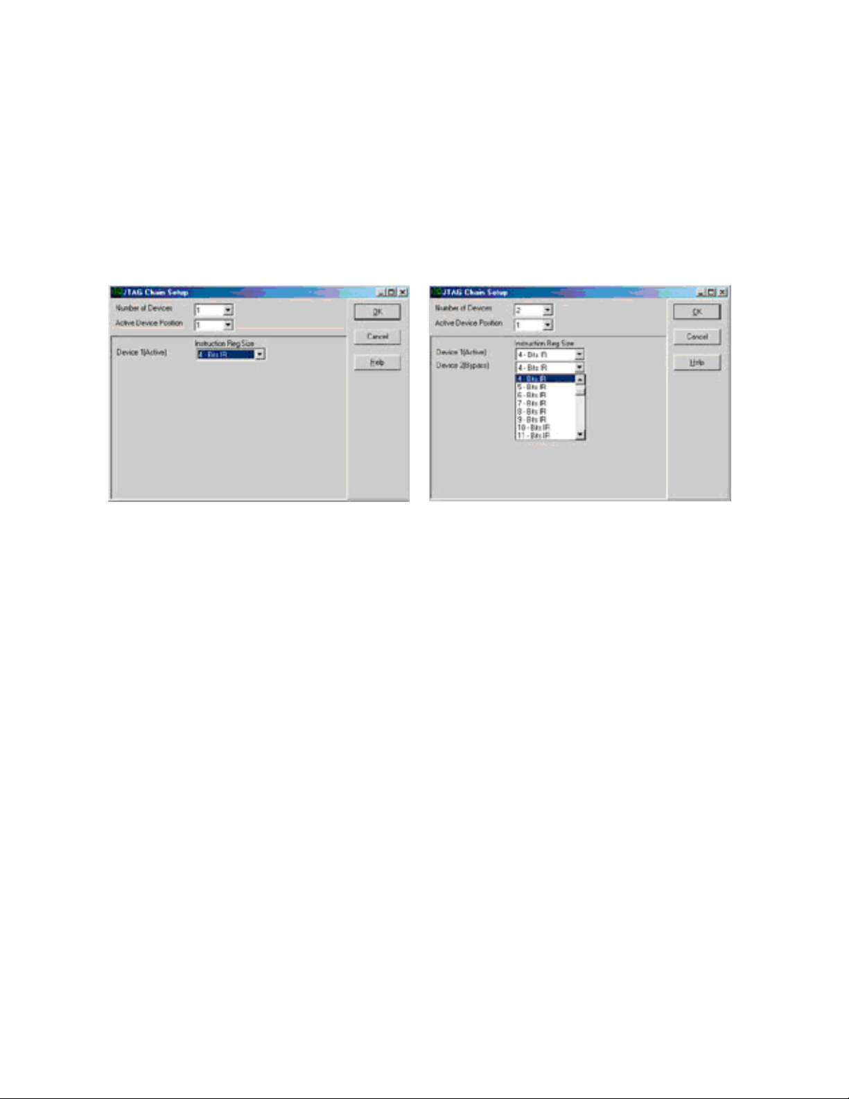
Figure 2-16: JTAG Chain Setup Screen.
Figure 2-17: Setup Screen with Two Devices
• JTAG Chain configuration is used if the ARM device is not the only chip connected to
the JTAG, or if the chip has multiple JTAG controllers (Figure 2-16).
– Number of JTAG devices:
This is the total number of devices connected to the JTAG Scan Chain. If only one
device is present, nothing needs to be configured.
– Configure:
This button is used to configure the number of devices and the Instruction Length for
each device. This is only available during the intial configuration. If you click the
Configure button, Figure 2-16 or Figure 2-17 appears depending on the number of
devices that were entered.
– Number of Devices:
This is used to set the total number of devices in the JTAG Scan Chain (Figure 2-17).
– Active Device Position:
This is used to set which device in the ARM chip the JTAG will connect to.
• Instruction Reg Size: There will be a drop down list for each of the devices. If the
number of devices is set to more than one, there will be a drop down list for each device
(Figure 2-17).
– Device1 (Active):
The Instruction Register size for the active device, which is automatically configured.
(ARM7 = 4, ARM9 = 5)
38
Page 39

– Device2(Bypass):
This is where the Instruction Register Length is set for the device in the chain that will
be bypassed.
Configuring the Emulator Options From Within Seehau
In Seehau, open the Emulator Configuration window. From the Config menu select Emulator.
The Emulator Configuration window opens displaying the Hdw Config tab (Figure 2-18).
Only the differences from the initial configuration will be discussed here.
The Emulator Configuration window contains three tabs. When selected, each tab allows you
to set the following options:
Hdw Cfg:
Misc Setup:
Map Config
Set up emulator hardware options.
Select reset options.
Used to manually set the address ranges where Thumb code is stored.
Buttons Common to All Tabs
OK: Saves the settings for the tab and exits the dialog box.
•
• Apply: Saves the settings for the tab.
• Cancel: Exits without saving the settings for the dialog box.
• Help: Displays the Seehau Help file.
• Refresh: Allows you to retrieve and view the current emulator hardware
configuration settings.
Figure 2-18: Emulator Configuration Window Displaying the Hdw Config Tab
39
Page 40

Hardware Configuration Tab
•
JTAG Chain
– The View button is used to check the current configuration. The configuration can
only be changed during the initial configuration.
Miscellaneous Setup Tab
The Misc Setup tab (Figure 2-19) is accessible only after the initial software configuration.
• Reset chip after load file:
Sets the ARM core to issue a reset after the code is loaded.
• Override at Reset
– The Program Counter option selects the value that the program counter will be set to
after the reset sequence has completed. Enter the program counter value in the box.
– The Stack Pointer option selects the value that the stack pointer will be set to after a
reset. Enter the stack pointer value in the box.
Figure 2-19: Emulator Configuration Window Displaying the Misc Setup Tab
40
Page 41

Map Config TAB
Figure 2-20 is accessible only after the initial software configuration. The file loader will
automatically map THUMB regions defined in the output file. This mapping window
provides a manual override for THUMB regions. The large open area displays the address
ranges that contain THUMB code.
• The Add button is used to add a range of memory that is used for THUMB code.
• The Edit button is available only when a range is selected. The range values may be
changed.
• The Remove button is used to delete one memory range from the table.
• The Remove All button is used to delete all the memory ranges from the table.
Figure 2-20: Emulator Configuration Window Displaying the Map Config Tab
41
Page 42

6. NAND Flash Programming
There is a button on the tool bar to start the NANDFlash Programming macro.
.
6.1 NAND Flash Programming Main Dialog Box
When you press this button the following screen should appear (figure 2-21)
Figure 2-21 NAND Flash Programming Main Dialog
42
Page 43

Field Description
Device Page Size The Page Size of the NAND Flash device is either Small or Large.
For Small Page device, the Page Size is 528 Byte ( x8 bus width ) / 264
Word ( x16 bus width ).
For Large Page device, the Page Size is 2112 Byte ( x8 bus width ) /
1056 Word ( x16 bus width ).
For Small Page device, three bus cycles are required to input the
addresses for devices having 256Mbit or less; four bus cycles are
required to input the addresses for devices having 512Mbit or more.
For Large Page device, four bus cycles are required to input the addresses
for devices having 1Gbit or less; five bus cycles are required to input the
addresses for devices having 2Gbit or more.
The NAND Flash device in the Philips LPC3000 Evaluation Board is
STMicroelectronics NAND256R3A which is a Small Page device.
Flash Device Size
Device is Lockable
Program Enable If this option is check it will enable any or all of the four program Image
The Philips LPC3000 supports x8 bus width only. The NAND Flash
devices supported by the Nohau SeehauARM NAND Flash
Programming Utility are 8MByte x 8 ( 64 Mbit ), 16MByte x 8 ( 128
Mbit ), 32MByte x 8 ( 256 Mbit ), 64MByte x 8 ( 512 Mbit ), 128MByte
x 8 ( 1 Gbit ), 256MByte x 8 ( 2 Gbit ), 512MByte x 8 ( 4 Gbit ), 1GByte
x 8 ( 8 Gbit ), 2GB x 8 ( 16 Gbit ).
The NAND Flash device in the Philips LPC3000 Evaluation Board is
STMicroelectronics NAND256R3A which is a 32MByte x 8 ( 256
Mbit ) device.
Most NAND Flash devices feature a Write Protect, /WP, pin, which
can be used to protect the device against program and erase
operations.
Additionally, some NAND Flash devices feature a Block Lock
mode, which is enabled by setting the Power-Up Read Enable,
Lock/Unlock Enable, PRL, pin to High. The Block Lock mode has
two levels of software protection - Blocks Lock/Unlock and Blocks
Lock-down.
The NAND Flash device in the Philips LPC3000 Evaluation
Board is STMicroelectronics NAND256R3A which does not
support the Block Lock mode.
files to be programmed into the memory during the Programming
process.
When you click on this option, if it is not checked, it will open another
dialog screen for additional settings. (Figure 2-22)
**Note**
43
Page 44

If checked, you will need to click if off then on to review the settings.
Select File buttons
If the Image File to Load is a Secondary Boot Loader, then it is
simply a binary image. The Nohau SeehauARM NAND Flash
Programming Utility will automatically generate necessary the
Interface Configuration Data.
The only Image File Option that can be used for the Secondary
Boot loader is Image 0.
6.2 NAND Flash Image Options Dialog Box
Figure 2-22 NAND Flash Image Options
44
Page 45

Field Description
Secondary Boot
Loader
Controller Type
Starting Block #
In the Philips LPC3000, there is a built in ROM of 16KB which
contains code to start running code from NAND FLASH or to
download code from UART to IRAM if in service mode. After
reset, execution begins from internal ROM. The program in the
ROM is called the Boot Code. The Boot Code SW first reads
input GPIO_01 (SERVICE_N). If GPIO_01 is high, the Boot Code
starts NAND FLASH booting. The image in the NAND Flash
device which is access by the Boot Code is referred as the
Secondary Boot Loader. For the flash boot procedure to work it
need to find the information ( Interface Configuration Data ) for,
how many page to copy and the type of flash that is connected.
The first page in the first block or the second block of the flash
shall contain the information (Interface Configuration Data )
needed for the flash boot code to work. If the Secondary Boot
Loader checkbox is checked, the Nohau SeehauARM NAND
Flash Programming Utility will automatically generate the
Interface Configuration Data. The Secondary Boot Loader is
simply a binary image which does not contain the Interface
Configuration Data.
The Philips LPC3000 has two NAND Flash Controllers, one (
MLC ) for multi level NAND Flash devices and one ( SLC ) for
single level NAND Flash devices. The two NAND Flash
Controllers use the same interface to the external NAND Flash
device.
It specifies the starting block position for the image to be
programmed into the NAND Flash device.
The NAND Flash devices are supplied with all the locations inside
valid blocks erased (FFh). The Bad Block Information is written
prior to shipping. The Nohau SeehauARM NAND Flash
Programming Utility uses Skip Block Method in the Bad Block
Management. In the Skip Block method the algorithm creates the
Bad Block Table and when the target address corresponds to a
Bad Block address, the data is stored in the next good block,
skipping the Bad Block. During the lifetime of the NAND device
additional Bad Blocks may develop. When a Bad Block is
generated during the lifetime of the NAND Flash device, it’s data
is also stored in the next good block. In this case, the information
that indicates which good block corresponds to each developed
Bad Block, also has to be stored in the NAND Flash device.
**Important Note**
If there are multiple images to be program into the device, then, in
order to avoid the overlapping of the images because of the Skip
45
Page 46

Block Method, the user should keep a reasonable margin when
specify the starting block position of the image.
ECC Generation
Enable
For MLC, it features HW support for Reed-Salomon
Encoding/Decoding (10 bit symbols), capable to correction of 4-symbol
( 4-40bit ), without SW needed.
For SLC, it features HW support for ECC (Error Checking and
Correction) on main area data. If an error is detected the SW must
correct it. The ECC on the spare area must be done in SW.
ECC Generation
Locations M10-M22
For SLC, the ECC ( 3Byte ) generation of the main area is done by HW and is
based on data blocks of 256Byte.
6.3 NAND Flash Erase
To erase a block or range of blocks in the NAND Flash you can click on the Erase NAND Flash
button on the Main Dialog Box. You will then see a screen like what is shown in figure 2.23.
Figure 2-23 NAND Flash Erase Dialog Box
Select the starting block number and a length of blocks to be erased. Enter a 1 for just a single
block.
46
Page 47

Appendix Figure 1
47
Page 48

48
Appendix Figure 2
Page 49

49
Appendix Figure 3
Page 50

50
Appendix Figure 4
Page 51

51
Appendix Figure 5
 Loading...