Philips J113, J111, J112 Datasheet

DISCRETE SEMICONDUCTORS
DATA SH EET
J111; J112; J113
N-channel silicon field-effect
transistors
Product specification
File under Discrete Semiconductors, SC07
July 1993

Philips Semiconductors Product specification
N-channel silicon field-effect transistors J111; J112; J113
DESCRIPTION
Symmetrical silicon n-channel
junction FETs in plastic TO-92
envelopes. They are intended for
applications such as analog switches,
choppers, commutators etc.
FEATURES
• High speed switching
• Interchangeability of drain and
source connections
• Low R
at zero gate voltage
DS on
PINNING
1 = gate
2 = source
3 = drain
Note: Drain and source are
interchangeable.
QUICK REFERENCE DATA
Drain-source voltage ±V
Drain current
VDS= 15 V; VGS=0 I
Total power dissipation
up to T
=50°CP
amb
Gate-source cut-off voltage
V
= 5 V; ID=1µA −V
DS
handbook, halfpage
1
2
3
MAM042
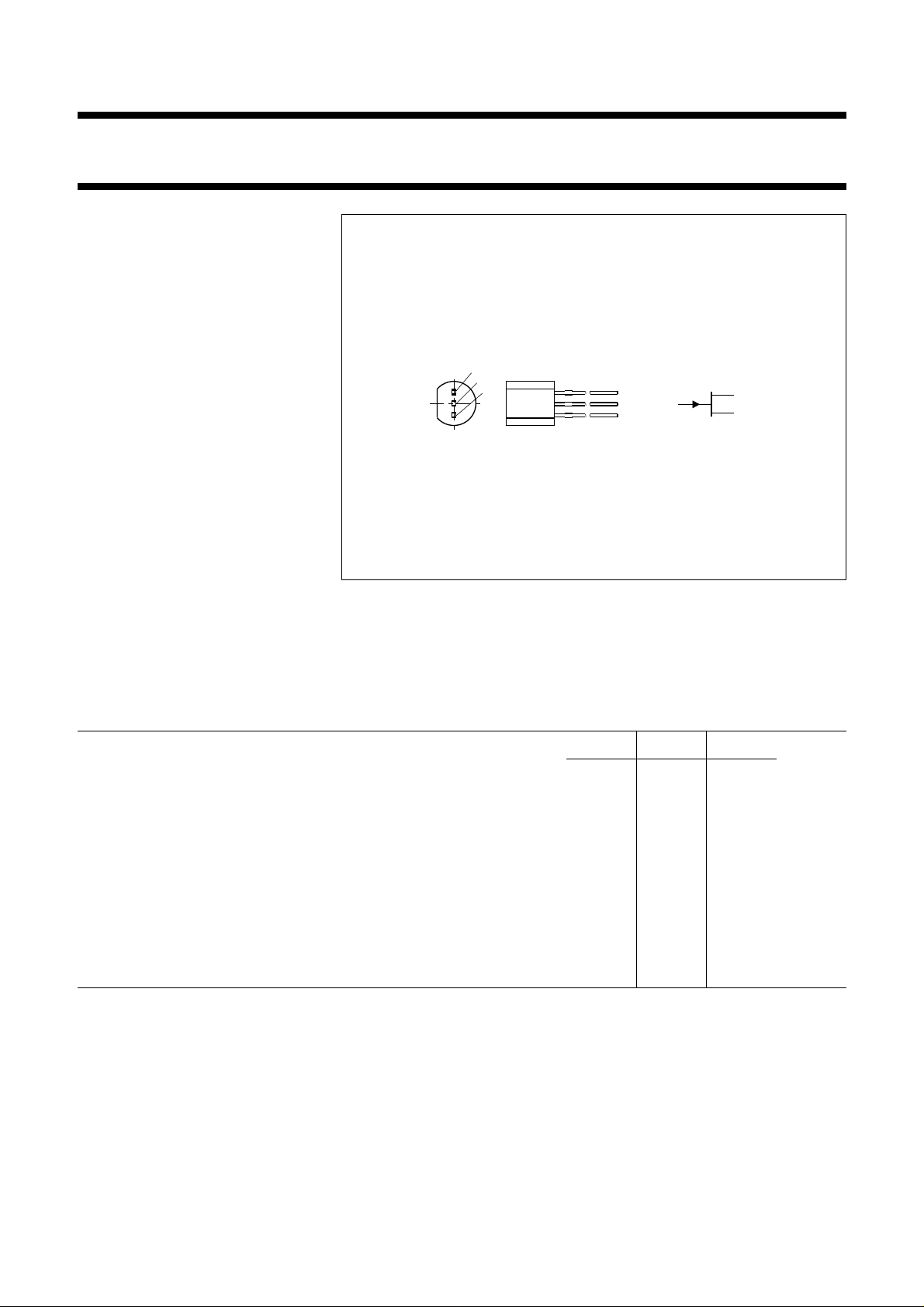
Fig.1 Simplified outline and symbol, TO-92.
J111 J112 J113
DS
DSS
tot
GS off
max. 40 40 40 V
min. 20 5 2 mA
max. 400 400 400 mW
min.
max.
3
10
g
1
5
d
s
0.53V
V
Drain-source on-state resistance
= 0.1 V; VGS=0 R
V
DS
DS on
July 1993 2
max. 30 50 100 Ω
 Loading...