

Page 1

ISP1761
Hi-Speed Universal Serial Bus On-The-Go controller
Rev. 01 — 12 January 2005 Product data sheet
1. General description
The ISP1761 is a single-chip Hi-Speed Universal Serial Bus (USB) On-The-Go (OTG)
Controller integrated with the advanced Philips Slave Host Controller and the Philips
ISP1582 Peripheral Controller.
2. Features
The Hi-Speed USB Host Controller and Peripheral Controller comply to
Bus Specification Rev. 2.0
Enhanced Host Controller Interface (EHCI) core implemented in the Host Controller is
adapted from
Rev. 1.0
Specification Rev. 1.0a
The ISP1761 has three USB ports. Port 1 can be configured to function as a downstream
port, an upstream port or an OTG port; ports 2 and 3 are always configured as
downstream ports. The OTG port can switch its role from host to peripheral, and
peripheral to host. The OTG port can become a host through the Host Negotiation
Protocol (HNP) as specified in the OTG supplement.
■ Compliant with
high-speed (480 Mbit/s), full-speed (12 Mbit/s) and low-speed (1.5 Mbit/s)
■ Integrated Transaction Translator (TT) for Original USB (full-speed and low-speed)
peripheral support
■ Three USB ports that support three operational modes:
◆ Mode 1: Port 1 is an OTG Controller port, and ports 2 and 3 are Host Controller
ports
◆ Mode 2: Ports 1, 2 and 3 are Host Controller ports
◆ Mode 3: Port 1 isaPeripheralController port, and ports 2 and 3 are Host Controller
ports
■ Supports OTG Host Negotiation Protocol (HNP) and Session Request Protocol (SRP)
■ Multitasking support with Virtual Segmentation feature (up to four banks)
■ High-speed memory controller (variable latency and SRAM external interface)
■ Directly addressable memory architecture
■ Generic processor interface to most CPUs, such as: Hitachi® SH-3 and SH-4, Philips
XA, Intel® StrongARM®, NEC® and Toshiba® MIPS, Motorola® DragonBall™ and
PowerPC® Reduced Instruction Set Computer (RISC) processors
■ Configurable 32-bit and 16-bit external memory data bus
■ Supports Programmed I/O (PIO) and Direct Memory Access (DMA)
■ Slave DMA implementation on CPU interface for reducing the host system’s CPU load
Enhanced Host Controller Interface Specification for Universal Serial Bus
. The OTG controller is compliant with
Universal Serial Bus Specification Rev. 2.0
and support data transfer speeds of up to 480 Mbit/s. The
On-The-Go Supplement to the USB
.
; supporting data transfer at
Universal Serial
Page 2

Philips Semiconductors
ISP1761
Hi-Speed USB OTG controller
■ Separate IRQ, DREQ and DACK lines for the Host Controller and the Peripheral
Controller
■ Integrated multiconfiguration FIFO
■ Double-buffering scheme increases throughput and facilitates real-time data transfer
■ Integrated Phase-Locked Loop (PLL) with external 12 MHz crystal for low EMI
■ Tolerant I/O for low voltage CPU interface (1.65 V to 3.3 V)
■ 3.3 V-to-5.0 V external power supply input
■ Integrated 5.0 V-to-1.8 V or 3.3 V-to-1.8 V voltage regulator (internal 1.8 V for
low-power core)
■ Internal power-on reset or low-voltage reset and block-dedicated software reset
■ Supports suspend and remote wake-up
■ Built-in overcurrent circuitry (analog overcurrent protection)
■ Hybrid-power mode: V
(can be switched off), V
CC(5V0)
CC(I/O)
(permanent)
■ Target total current consumption:
◆ Normal operation; one port in high-speed active: ICC< 100 mA when the internal
charge pump is not used
◆ Suspend mode: I
CC(susp)
< 150 µA at the room temperature
■ Available in LQFP128 and TFBGA128 packages
■ Host Controller-specific features
◆ High performance USB host with integrated high-speed USB transceivers;
supports high-speed, full-speed and low-speed
◆ The EHCI core is adapted from
Enhanced Host Controller Interface Specification
for Universal Serial Bus Rev. 1.0
◆ Configurable power management
◆ Integrated TT for Original USB peripheral support on all three ports
◆ Integrated 64 kB high-speed memory (internally organized as 8kX64bits)
◆ Additional 2.5 kB separate memory for TT
◆ Individual or global overcurrent protection with built-in sense circuits
◆ Overcurrent circuitry built-in (digital or analog overcurrent protection)
■ OTG Controller-specific features
◆ OTG transceiver: fully integrated; compliant with
On-The-Go Supplement to the
USB Specification Rev. 1.0a
◆ Supports HNP and SRP for OTG dual-role devices
◆ HNP: status and control registers for software implementation
◆ SRP: status and control registers for software implementation
◆ Programmable timers with high resolution (0.01 ms to 80 ms)—for HNP and SRP
◆ Supports external source of V
BUS
■ Peripheral Controller-specific features
◆ High-performance USB Peripheral Controller with integrated Serial Interface
Engine (SIE), FIFO memory and transceiver
◆ Complies with
Universal Serial Bus Specification Rev. 2.0
and most device class
specifications
◆ Supports auto Hi-Speed USB mode discovery and Original USB fallback
capabilities
◆ Supports high-speed and full-speed on the Peripheral Controller
◆ Bus-powered or self-powered capability with suspend mode
9397 750 13258 © Koninklijke Philips Electronics N.V. 2005. All rights reserved.
Product data sheet Rev. 01 — 12 January 2005 2 of 158
Page 3

Philips Semiconductors
◆ Slave DMA, fully autonomous and supports multiple configurations
◆ Seven IN endpoints, seven OUT endpoints and one fixed control IN and OUT
◆ Integrated 8 kB memory
◆ Software-controllable connection to the USB bus, SoftConnect™
3. Applications
The ISP1761 can be used to implement a dual-role USB device in any application—USB
host or USB peripheral—depending on the cable connection. If the dual-role device is
connected to a typical USB peripheral, it behaves like a typical USB host. The dual-role
device can also be connected to a PC or any other USB host and behave like a typical
USB peripheral.
3.1 Host/peripheral roles
■ Mobile phone to/from:
◆ Mobile phone: exchange contact information
◆ Digital still camera: e-mail pictures or upload pictures to the web
◆ MP3 player: upload/download/broadcast music
◆ Mass storage: upload/download files
◆ Scanner: scan business cards
■ Digital still camera to/from:
◆ Digital still camera: exchange pictures
◆ Mobile phone: e-mail pictures, upload pictures to the web
◆ Printer: print pictures
◆ Mass storage: store pictures
■ Printer to/from:
◆ Digital still camera: print pictures
◆ Scanner: print scanned image
◆ Mass storage: print files stored in a device
■ MP3 player to/from:
◆ MP3 player: exchange songs
◆ Mass storage: upload/download songs
■ Oscilloscope to/from:
◆ Printer: print screen image
■ Personal digital assistant to/from:
◆ Personal digital assistant: exchange files
◆ Printer: print files
◆ Mobile phone: upload/download files
◆ MP3 player: upload/download songs
◆ Scanner: scan pictures
◆ Mass storage: upload/download files
◆ Global Positioning System (GPS): obtain directions, mapping information
◆ Digital still camera: upload pictures
◆ Oscilloscope: configure oscilloscope
ISP1761
Hi-Speed USB OTG controller
endpoint
9397 750 13258 © Koninklijke Philips Electronics N.V. 2005. All rights reserved.
Product data sheet Rev. 01 — 12 January 2005 3 of 158
Page 4

Philips Semiconductors
4. Ordering information
Table 1: Ordering information
Type number Package
ISP1761BE LQFP128 plastic low profile quad flat package; 128 leads;
ISP1761ET
[1] The ISP1761ET is currently under development.
[1]
ISP1761
Hi-Speed USB OTG controller
Name Description Version
SOT425-1
body 14 x 20 x 1.4 mm
TFBGA128 plastic thin fine-pitch ball grid array package;
128 balls; body 9x9x0.8mm
SOT857-1
9397 750 13258 © Koninklijke Philips Electronics N.V. 2005. All rights reserved.
Product data sheet Rev. 01 — 12 January 2005 4 of 158
Page 5
Philips Semiconductors
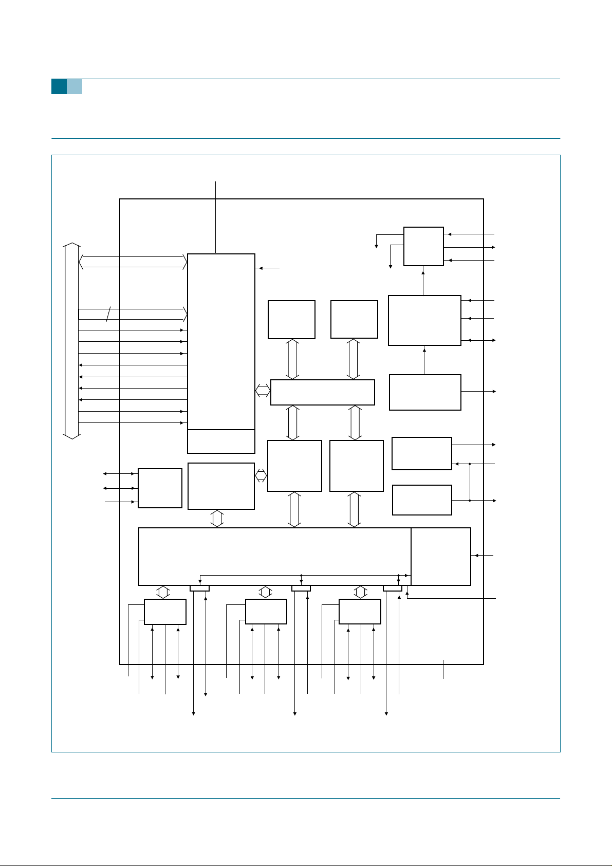
5. Block diagram
V
CC(I/O)
ISP1761
Hi-Speed USB OTG controller
37 to 39, 41 to 43,
45 to 47, 49, 51,
52, 54, 56 to 58,
60 to 62, 64 to 66,
68 to 70, 72 to 74,
76 to 78, 80
D[15:0]/D[31:0]
82, 84, 86, 87,
17
89, 91 to 93,
95 to 98,
100 to 103, 105
A[17:1]
106
107
108
111
112
113
114
116
117
124
125
CHARGE
PUMP
126
GENERIC PROCESSOR BUS
CS_N
RD_N
WR_N
DC_IRQ
HC_IRQ
DC_DREQ
HC_DREQ
HC_DACK
DC_DACK
C_B
C_A
V
CC(C_IN)
10, 40, 48, 59, 67,
75, 83, 94, 104, 115
BUS INTERFACE:
MEMORY
MANAGEMENT
UNIT
+
SLAVE DMA
CONTROLLER
+
INTERRUPT
CONTROL
REGISTERS
SUPPORT
TRANSACTION
TRANSLATOR
(TT) AND RAM
ISP1761
SEL16/32
HC BUFFER
MEMORY
64 KBYTES
MEMORY ARBITER
AND FIFO
ADVANCED
PHILIPS
SLAVE HOST
CONTROLLER
30 MHz
DC BUFFER
MEMORY
8 KBYTES
ADVANCED
PERIPHERAL
CONTROLLER
PLL
60 MHz
GLOBAL CONTROL
AND POWER
MANAGEMENT
POWER-ON
RESET AND
V
BAT
5 V-TO-1.8 V
VOLTAGE
REGULATOR
5 V-TO-3.3 V
VOLTAGE
REGULATOR
ON
11
12
13
122
119
120
110
5, 50,
85, 118
6, 7
9
XTAL1
XTAL2
CLKIN
RESET_N
HC_SUSPEND/
WAKEUP_N
DC_SUSPEND/
WAKEUP_N
V
BAT_ON_N
V
REG(1V8)
V
CC(5V0)
V
REG(3V3)
DIGITAL
AND ANALOG
OVERCURRENT
PROTECTION
4, 8, 14, 17, 24,
31, 36, 44, 53,
55, 63, 71, 79,
88, 90, 99, 109,
121, 123
1
GND
2
3
004aaa450
REF5V
ID
16
RREF1
GND
HI-SPEED
USB ATX1
15
20
DP1
GND
OTG CONTROLLER
DYNAMIC PORT ROUTING AND PORT CONTROL LOGIC
HI-SPEED
USB ATX2
19
DM1
21
18
OC1_N/
PSW1_N
V
127
RREF2
BUS
23
GND
22
DP2
27
GND
26
DM2
PSW2_N
128
28
25
RREF3
OC2_N
30
GND
HI-SPEED
USB ATX3
29
34
DP3
GND
32
33
DM3
PSW3_N
35
OC3_N
Fig 1. Block diagram
9397 750 13258 © Koninklijke Philips Electronics N.V. 2005. All rights reserved.
Product data sheet Rev. 01 — 12 January 2005 5 of 158
Page 6
Philips Semiconductors
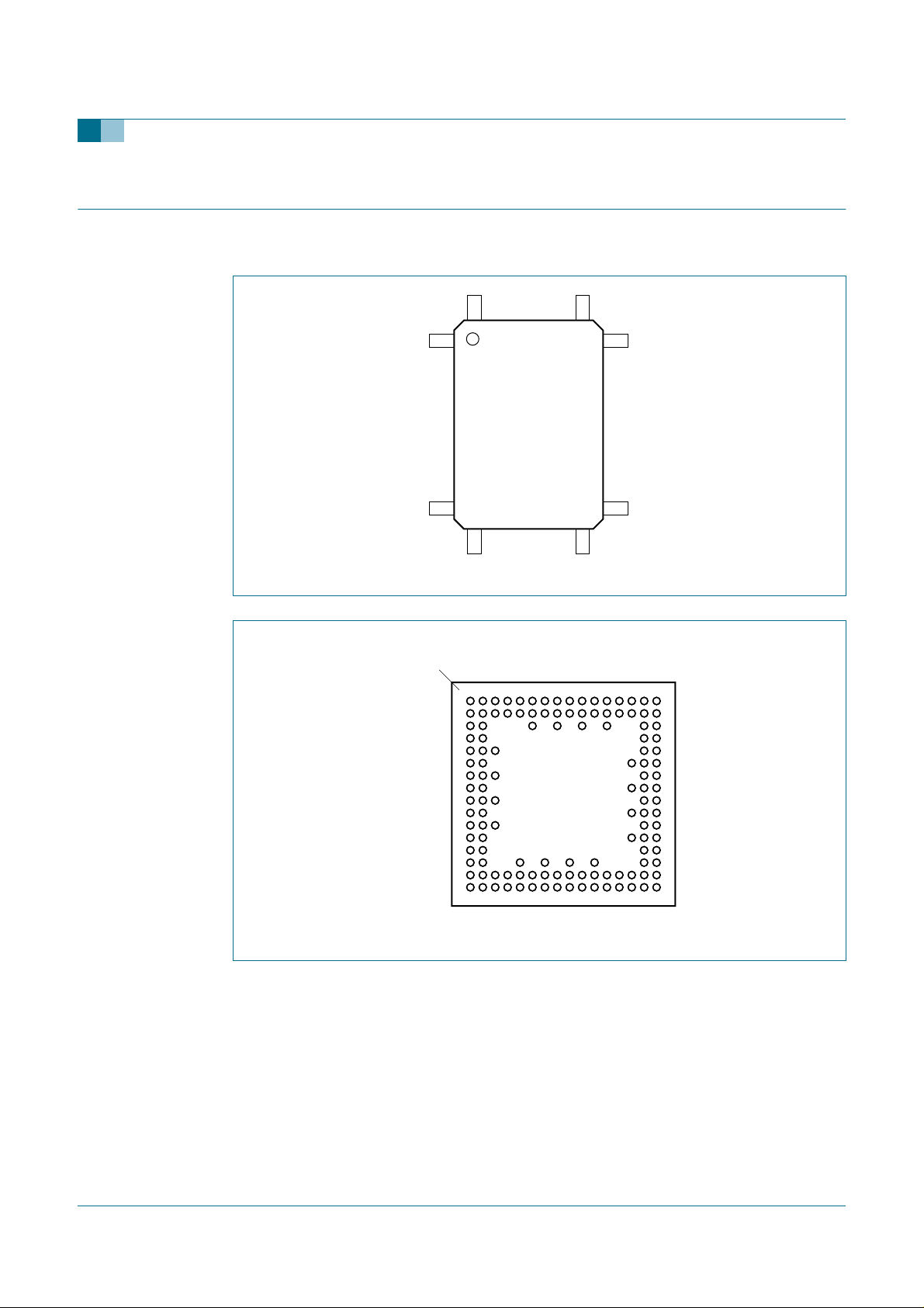
6. Pinning information
6.1 Pinning
ISP1761
Hi-Speed USB OTG controller
128
1
ISP1761BE
38
39
Fig 2. Pin configuration (LQFP128); top view
ball A1
index area
B
D
H
K
M
2468101213141516
1357911
A
C
E
F
G
J
L
N
P
R
T
ISP1761ET
103
64
004aaa506
102
65
004aaa551
Fig 3. Pin configuration (TFBGA128); top view
9397 750 13258 © Koninklijke Philips Electronics N.V. 2005. All rights reserved.
Product data sheet Rev. 01 — 12 January 2005 6 of 158
Page 7

Philips Semiconductors
ISP1761
Hi-Speed USB OTG controller
6.2 Pin description
Table 2: Pin description
Symbol
[1]
Pin
LQFP128
Ball
TFBGA128
OC3_N 1 C2 AI/I port 3 analog (5 V input) and digital overcurrent input; if not used,
REF5V 2 A2 AI 5 V reference input for analog OC detector; connect a 100 nF
ID 3 B2 I ID input for detection of the default host or peripheral setting when
GND 4 A1 - analog ground
V
REG(1V8)
V
CC(5V0)
V
CC(5V0)
5 B1 P corepoweroutput (1.8 V); internal 1.8 V forthe digital core; used for
6 C1 P input to internal regulators (3.0 V to 5.5 V); connect a 100 nF
7 D2 P input to internal regulators (3.0 V to 5.5 V); connect a 100 nF
GND 8 E3 - oscillator ground
V
REG(3V3)
V
CC(I/O)
9 D1 P regulator output (3.3 V); for decoupling only; connect a 100 nF
10 E2 P digital supply; 1.65 V to 3.6 V; connect a 100 nF decoupling
XTAL1 11 E1 AI 12 MHz crystal connection input; connect to ground if an external
XTAL2 12 F2 AO 12 MHz crystal connection output
CLKIN 13 F1 I 12 MHz oscillator or clock input; connect to V
GND 14 G3 - digital ground
GND 15 G2 - RREF1 ground
RREF1 16 G1 AI reference resistor connection; connect a 12 kΩ±1 % resistor
GND 17 H2 - analog ground for port 1
DM1 18 H1 AI/O downstream data minus port 1
GND 19 J3 - analog ground
DP1 20 J2 AI/O downstream data plus port 1
PSW1_N 21 J1 OD power switch port 1, active LOW
GND 22 K2 - RREF2 ground
RREF2 23 K1 AI reference resistor connection; connect a 12 kΩ±1 % resistor
GND 24 L3 - analog ground for port 2
DM2 25 L1 AI/O downstream data minus port 2
GND 26 L2 - analog ground
Type
[2]
Description
connect to V
through a 10 kΩ resistor
CC(I/O)
input, 3.3 V tolerant
decoupling capacitor
port 1 is in the OTG mode
input, 3.3 V tolerant
decoupling; connect a 100 nF capacitor; for details on additional
capacitor placement, see
decoupling capacitor; see
decoupling capacitor; see
capacitor and a 4.7 µFto10µF capacitor; see
capacitor; see
Section 7.7
Section 7.7
Section 7.7
Section 7.7
Section 7.7
clock is used
CC(I/O)
3.3 V tolerant
between this pin and the RREF1 ground
output pad, push-pull open-drain, 8 mA output drive, 5 V tolerant
between this pin and the RREF2 ground
when not in use
9397 750 13258 © Koninklijke Philips Electronics N.V. 2005. All rights reserved.
Product data sheet Rev. 01 — 12 January 2005 7 of 158
Page 8

Philips Semiconductors
ISP1761
Hi-Speed USB OTG controller
Table 2: Pin description
CC(I/O)
[1]
Pin
LQFP128
40 T4 P digital supply; 1.65 V to 3.6 V; connect a 100 nF decoupling
Symbol
DP2 27 M2 AI/O downstream data plus port 2
PSW2_N 28 M1 OD power switch port 2, active LOW
GND 29 N2 - RREF3 ground
RREF3 30 N1 AI reference resistor connection; connect a 12 kΩ±1 % resistor
GND 31 P2 - analog ground for port 3
DM3 32 P1 AI/O downstream data minus port 3
GND 33 R2 - analog ground
DP3 34 R1 AI/O downstream data plus port 3
PSW3_N 35 T1 OD power switch port 3, active LOW
GND 36 T2 - digital ground
DATA0 37 R3 I/O data bit 0 input and output
DATA1 38 T3 I/O data bit 1 input and output
DATA2 39 R4 I/O data bit 2 input and output
V
DATA3 41 P5 I/O data bit 3 input and output
DATA4 42 T5 I/O data bit 4 input and output
DATA5 43 R5 I/O data bit 5 input and output
GND 44 T6 - digital ground
DATA6 45 R6 I/O data bit 6 input and output
DATA7 46 P7 I/O data bit 7 input and output
DATA8 47 T7 I/O data bit 8 input and output
…continued
Ball
TFBGA128
Type
[2]
Description
output pad, push-pull open-drain, 8 mA output drive, 5 V tolerant
between this pin and the RREF3 ground
output pad, push-pull open-drain, 8 mA output drive, 5 V tolerant
bidirectional pad, push-pull input, three-state output, 4 mA output
drive, 3.3 V tolerant
bidirectional pad, push-pull input, three-state output, 4 mA output
drive, 3.3 V tolerant
bidirectional pad, push-pull input, three-state output, 4 mA output
drive, 3.3 V tolerant
capacitor; see
bidirectional pad, push-pull input, three-state output, 4 mA output
drive, 3.3 V tolerant
bidirectional pad, push-pull input, three-state output, 4 mA output
drive, 3.3 V tolerant
bidirectional pad, push-pull input, three-state output, 4 mA output
drive, 3.3 V tolerant
bidirectional pad, push-pull input, three-state output, 4 mA output
drive, 3.3 V tolerant
bidirectional pad, push-pull input, three-state output, 4 mA output
drive, 3.3 V tolerant
bidirectional pad, push-pull input, three-state output, 4 mA output
drive, 3.3 V tolerant
Section 7.7
9397 750 13258 © Koninklijke Philips Electronics N.V. 2005. All rights reserved.
Product data sheet Rev. 01 — 12 January 2005 8 of 158
Page 9

Philips Semiconductors
ISP1761
Hi-Speed USB OTG controller
Table 2: Pin description
Symbol
[1]
Pin
LQFP128
V
CC(I/O)
48 R7 P digital supply; 1.65 V to 3.6 V; connect a 100 nF decoupling
…continued
Ball
TFBGA128
Type
[2]
Description
capacitor; see
Section 7.7
DATA9 49 T8 I/O data bit 9 input and output
bidirectional pad, push-pull input, three-state output, 4 mA output
drive, 3.3 V tolerant
V
REG(1V8)
50 R8 P core power output (1.8 V); internal 1.8 V for the digital core; used for
decoupling; connect a 100 nF capacitor; for details on additional
capacitor placement, see
DATA10 51 P9 I/O data bit 10 input and output
bidirectional pad, push-pull input, three-state output, 4 mA output
drive, 3.3 V tolerant
DATA11 52 T9 I/O data bit 11 input and output
bidirectional pad, push-pull input, three-state output, 4 mA output
drive, 3.3 V tolerant
GND 53 R9 - core ground
DATA12 54 T10 I/O data bit 12 input and output
bidirectional pad, push-pull input, three-state output, 4 mA output
drive, 3.3 V tolerant
GND 55 R10 - digital ground
DATA13 56 P11 I/O data bit 13 input and output
bidirectional pad, push-pull input, three-state output, 4 mA output
drive, 3.3 V tolerant
DATA14 57 T11 I/O data bit 14 input and output
bidirectional pad, push-pull input, three-state output, 4 mA output
drive, 3.3 V tolerant
DATA15 58 R11 I/O data bit 15 input and output
bidirectional pad, push-pull input, three-state output, 4 mA output
drive, 3.3 V tolerant
V
CC(I/O)
59 T12 P digital supply; 1.65 V to 3.6 V; connect a 100 nF decoupling
capacitor; see
Section 7.7
DATA16 60 R12 I/O data bit 16 input and output
bidirectional pad, push-pull input, three-state output, 4 mA output
drive, 3.3 V tolerant
DATA17 61 T13 I/O data bit 17 input and output
bidirectional pad, push-pull input, three-state output, 4 mA output
drive, 3.3 V tolerant
DATA18 62 R13 I/O data bit 18 input and output
bidirectional pad, push-pull input, three-state output, 4 mA output
drive, 3.3 V tolerant
GND 63 R14 - digital ground
DATA19 64 T14 I/O data bit 19 input and output
bidirectional pad, push-pull input, three-state output, 4 mA output
drive, 3.3 V tolerant
Section 7.7
9397 750 13258 © Koninklijke Philips Electronics N.V. 2005. All rights reserved.
Product data sheet Rev. 01 — 12 January 2005 9 of 158
Page 10

Philips Semiconductors
ISP1761
Hi-Speed USB OTG controller
Table 2: Pin description
CC(I/O)
CC(I/O)
[1]
Pin
LQFP128
67 P15 P digital supply; 1.65 V to 3.6 V; connect a 100 nF decoupling
75 M14 P digital supply; 1.65 V to 3.6 V; connect a 100 nF decoupling
Symbol
DATA20 65 T15 I/O data bit 20 input and output
DATA21 66 R15 I/O data bit 21 input and output
V
DATA22 68 T16 I/O data bit 22 input and output
DATA23 69 R16 I/O data bit 23 input and output
DATA24 70 P16 I/O data bit 24 input and output
GND 71 N16 - digital ground
DATA25 72 N15 I/O data bit 25 input and output
DATA26 73 M15 I/O data bit 26 input and output
DATA27 74 M16 I/O data bit 27 input and output
V
DATA28 76 L16 I/O data bit 28 input and output
DATA29 77 L15 I/O data bit 29 input and output
DATA30 78 K16 I/O data bit 30 input and output
GND 79 K15 - digital ground
DATA31 80 K14 I/O data bit 31 input and output
TEST 81 J16 - connect to ground
A1 82 H16 I address pin 1
…continued
Ball
TFBGA128
Type
[2]
Description
bidirectional pad, push-pull input, three-state output, 4 mA output
drive, 3.3 V tolerant
bidirectional pad, push-pull input, three-state output, 4 mA output
drive, 3.3 V tolerant
capacitor; see
bidirectional pad, push-pull input, three-state output, 4 mA output
drive, 3.3 V tolerant
bidirectional pad, push-pull input, three-state output, 4 mA output
drive, 3.3 V tolerant
bidirectional pad, push-pull input, three-state output, 4 mA output
drive, 3.3 V tolerant
bidirectional pad, push-pull input, three-state output, 4 mA output
drive, 3.3 V tolerant
bidirectional pad, push-pull input, three-state output, 4 mA output
drive, 3.3 V tolerant
bidirectional pad, push-pull input, three-state output, 4 mA output
drive, 3.3 V tolerant
capacitor; see
bidirectional pad, push-pull input, three-state output, 4 mA output
drive, 3.3 V tolerant
bidirectional pad, push-pull input, three-state output, 4 mA output
drive, 3.3 V tolerant
bidirectional pad, push-pull input, three-state output, 4 mA output
drive, 3.3 V tolerant
bidirectional pad, push-pull input, three-state output, 4 mA output
drive, 3.3 V tolerant
input, 3.3 V tolerant
Section 7.7
Section 7.7
9397 750 13258 © Koninklijke Philips Electronics N.V. 2005. All rights reserved.
Product data sheet Rev. 01 — 12 January 2005 10 of 158
Page 11

Philips Semiconductors
ISP1761
Hi-Speed USB OTG controller
Table 2: Pin description
Symbol
[1]
Pin
LQFP128
V
CC(I/O)
83 J15 P digital supply; 1.65 V to 3.6 V; connect a 100 nF decoupling
…continued
Ball
TFBGA128
Type
[2]
Description
capacitor; see
A2 84 H15 I address pin 2
input, 3.3 V tolerant
V
REG(1V8)
85 G16 P core power output (1.8 V); internal 1.8 V for the digital core; used for
decoupling; connect a 100 nF capacitor and a 4.7 µFto10µF
capacitor; see
A3 86 H14 I address pin 3
input, 3.3 V tolerant
A4 87 F16 I address pin 4
input, 3.3 V tolerant
GND 88 G15 - core ground
A5 89 F15 I address pin 5
input, 3.3 V tolerant
GND 90 E16 - digital ground
A6 91 F14 I address pin 6
input, 3.3 V tolerant
A7 92 E15 I address pin 7
input, 3.3 V tolerant
A8 93 D16 I address pin 8
input, 3.3 V tolerant
V
CC(I/O)
94 D15 P digital supply; 1.65 V to 3.6 V; connect a 100 nF decoupling
capacitor; see
A9 95 C16 I address pin 9
input, 3.3 V tolerant
A10 96 C15 I address pin 10
input, 3.3 V tolerant
A11 97 B16 I address pin 11
input, 3.3 V tolerant
A12 98 B15 I address pin 12
input, 3.3 V tolerant
GND 99 A16 - digital ground
A13 100 A15 I address pin 13
input, 3.3 V tolerant
A14 101 B14 I address pin 14
input, 3.3 V tolerant
A15 102 A14 I address pin 15
input, 3.3 V tolerant
A16 103 A13 I address pin 16
input, 3.3 V tolerant
V
CC(I/O)
104 B13 P digital voltage; 1.65 V to 3.6 V; connect a 100 nF decoupling
capacitor; see
Section 7.7
Section 7.7
Section 7.7
Section 7.7
9397 750 13258 © Koninklijke Philips Electronics N.V. 2005. All rights reserved.
Product data sheet Rev. 01 — 12 January 2005 11 of 158
Page 12

Philips Semiconductors
ISP1761
Hi-Speed USB OTG controller
Table 2: Pin description
Symbol
[1]
Pin
LQFP128
…continued
Ball
TFBGA128
Type
[2]
Description
A17 105 C12 I address pin 17
input, 3.3 V tolerant
CS_N 106 A12 I chip select signal that indicates the area being accessed; active
LOW
input, 3.3 V tolerant
RD_N 107 B12 I read enable; active LOW
input, 3.3 V tolerant
WR_N 108 B11 I write enable; active LOW
input, 3.3 V tolerant
GND 109 A11 - digital ground
V
BAT_ON_N
110 C10 OD to indicate the presence of a minimum 3.3 V on pins 6 and 7
(open-drain); connect to V
through a 10 kΩ pull-up resistor
CC(I/O)
output pad, push-pull open-drain, 8 mA output drive, 5 V tolerant
DC_IRQ 111 A10 O Peripheral Controller interrupt signal
output 4 mA drive, 3.3 V tolerant
HC_IRQ 112 B10 O Host Controller interrupt signal
output 4 mA drive, 3.3 V tolerant
DC_DREQ 113 A9 O DMAC request for the Peripheral Controller
output 4 mA drive, 3.3 V tolerant
HC_DREQ 114 B9 O DMAC request for Host Controller
output 4 mA drive, 3.3 V tolerant
V
CC(I/O)
115 C8 P digital voltage; 1.65 V to 3.6 V; connect a 100 nF decoupling
capacitor; see
Section 7.7
HC_DACK 116 A8 I Host Controller DMA request acknowledgment; when not in use,
connect to V
through a 10 kΩ pull-up resistor
CC(I/O)
input, 3.3 V tolerant
DC_DACK 117 B8 I Peripheral Controller DMA request acknowledgment; when not in
use, connect to V
through a 10 kΩ pull-up resistor
CC(I/O)
input, 3.3 V tolerant
V
REG(1V8)
118 B7 P core power output (1.8 V); internal 1.8 V for the digital core; used for
decoupling; connect a 100 nF capacitor; for details on additional
HC_SUSPEND
/WAKEUP_N
capacitor placement, see
119 A7 I/OD Host Controller suspend and wake-up; three-state suspend output
(active LOW) and wake-up input circuits are connected together
Section 7.7
• HIGH = output is three-state; ISP1761 is in suspend mode
• LOW = output is LOW; ISP1761 is not in suspend mode.
connect to V
output pad, open-drain, 4 mA output drive, 3.3 V tolerant
through an external 10 kΩ pull-up resistor
CC(I/O)
9397 750 13258 © Koninklijke Philips Electronics N.V. 2005. All rights reserved.
Product data sheet Rev. 01 — 12 January 2005 12 of 158
Page 13

Philips Semiconductors
ISP1761
Hi-Speed USB OTG controller
Table 2: Pin description
Symbol
DC_SUSPEND
/WAKEUP_N
[1]
Pin
LQFP128
120 C6 I/OD Peripheral Controller suspend and wake-up; three-state suspend
…continued
Ball
TFBGA128
Type
[2]
Description
output (active LOW) and wake-up input circuits are connected
together
• HIGH = output is three-state; ISP1761 is in suspend mode
• LOW = output is LOW; ISP1761 is not in suspend mode.
connect to V
output pad, open-drain, 4 mA output drive, 3.3 V tolerant
GND 121 A6 - core ground
RESET_N 122 B6 I external power-up reset; active LOW
input, 3.3 V tolerant
Remark: During reset, ensure that all the input pins to the ISP1761
are not toggling.
GND 123 B5 - analog ground
C_B 124 A5 AI/O charge pump capacitor input; connect a 220 nF capacitor between
this pin and pin 125
C_A 125 B4 AI/O charge pump capacitor input; connect a 220 nF capacitor between
this pin and pin 124
V
CC(C_IN)
OC1_N/V
BUS
126 A4 P charge pump input; connect to 3.3 V
127 B3 (AI/O)(I) This pin has multiple functions:
through an external 10 kΩ pull-up resistor
CC(I/O)
• Port 1 OC1_N detection when port 1 is configured for host
functionality and an external power switch is used; connect to
V
through a 10 kΩ resistor
CC(I/O)
• V
• V
input, 3.3 V tolerant
OC2_N 128 A3 AI/I port 2 analog (5 V input) and digital overcurrent input; if not used,
connect to V
input, 3.3 V tolerant
out when internal charge pump is used and port 1 is
BUS
configured for the host functionality; maximum 50 mA current
capability; only for port 1
input detection when port 1 is defined for the peripheral
BUS
functionality.
through a 10 kΩ resistor
CC(I/O)
[1] Symbol names ending with underscore N (for example, NAME_N) represent active LOW signals.
[2] I = input only; O = output only; I/O = digital input/output; OD = open-drain output; AI/O = analog input/output; AI = analog input;
P = power; (AI/O)(I) = analog input/output digital input; AI/I = analog input digital input.
9397 750 13258 © Koninklijke Philips Electronics N.V. 2005. All rights reserved.
Product data sheet Rev. 01 — 12 January 2005 13 of 158
Page 14

Philips Semiconductors
7. Functional description
7.1 ISP1761 internal architecture: Advanced Philips Slave Host Controller and hub
The EHCI block and the Hi-Speed USB hub block are the main components of the
Advanced Philips Slave Host Controller.
The EHCI is the latest generation design, with improved data bandwidth. The EHCI in the
ISP1761 is adapted from
Serial Bus Rev. 1.0
The internal Hi-Speed USB hub block replaces the companion Host Controller block used
in the original architecture of a Peripheral Component Interconnect (PCI) Hi-Speed USB
Host Controller to handle the full-speed and low-speed modes. The hardware architecture
in the ISP1761 is simplified to help reduce cost and development time, by eliminating the
additional work involved in implementing the OHCI software required to support the
full-speed and low-speed modes.
Figure 4 shows the internal architecture of the ISP1761. The ISP1761 implements an
EHCI that has an internal port—the Root Hub port (not availableexternally)—on which the
internal hub is connected. The three external ports are always routed to the internal hub.
The internal hub is a Hi-Speed USB hub including the TT.
ISP1761
Hi-Speed USB OTG controller
Enhanced Host Controller Interface Specification for Universal
.
Remark: The root hub must be enabled and the internal hub must be enumerated.
Enumerate the internal hub as if it is externally connected. For details, refer to
Linux Programming Guide (AN10042)
At the Host Controller reset and initialization, the internal Root Hub port will be polled until
a new connection is detected, showing the connection of the internal hub.
The internal Hi-Speed USB hub is enumerated using a sequence similar to a standard
Hi-Speed USB hub enumeration sequence, and the polling on the Root Hub is stopped
because the internal Hi-Speed USB hub will never be disconnected. When enumerated,
the internal hub will report the three externally available ports.
.
ISP176x
9397 750 13258 © Koninklijke Philips Electronics N.V. 2005. All rights reserved.
Product data sheet Rev. 01 — 12 January 2005 14 of 158
Page 15
Philips Semiconductors
ISP1761
Hi-Speed USB OTG controller
EHCI
ROOT HUB
PORTSC1
ENUMERATION
AND POLLING USING
ACTUAL PTDs
INTERNAL HUB (TT)
PORT1
Fig 4. Internal hub
7.1.1 Internal clock scheme
Figure 5 shows the internal clock scheme of the ISP1761. The ISP1761 has three ports.
XOSC
PORT2
PORT 2
PORT 1
ATX
peripheral clock:
ATX
PORT3
host clock:
48 MHz,
30 MHz,
60 MHz
48 MHz,
30 MHz,
60 MHz
EXTERNAL
PORTS
004aaa513
DIGITAL
CORE
HOST
CORE
PERIPHERAL
CORE
004aaa538
PORT 3
PLL 12 MHz IN
ATX
Fig 5. ISP1761 clock scheme
9397 750 13258 © Koninklijke Philips Electronics N.V. 2005. All rights reserved.
Product data sheet Rev. 01 — 12 January 2005 15 of 158
Page 16

Philips Semiconductors
Hi-Speed USB OTG controller
Port 2 does not need to be enabled using software if only port 1 or port 3 is used. No port
needs to be disabled by external pull-up resistors, if not used. The DP and DM of the
unused ports need not be externally pulled HIGH because there are internal pull-down
resistors on each port that are enabled by default.
Table 3 lists the various port connection scenarios.
Table 3: Port connection scenarios
Port configuration Port 1 Port 2 Port 3
One port (port 1) DP and DM are routed to USB
connector
One port (port 2) DP and DM are not connected
(left open)
One port (port 3) DP and DM are not connected
(left open)
Two ports
(ports 1 and 2)
Two ports
(ports 2 and 3)
Two ports
(ports 1 and 3)
Three ports
(ports 1, 2 and 3)
DP and DM are routed to USB
connector
DP and DM are not connected
(left open)
DP and DM are routed to USB
connector
DP and DM are routed to USB
connector
DP and DM are not connected
(left open)
DP and DM are routed to USB
connector
DP and DM are not connected
(left open)
DP and DM are routed to USB
connector
DP and DM are routed to USB
connector
DP and DM are not connected
(left open)
DP and DM are routed to USB
connector
DP and DM are not connected
(left open)
DP and DM are not connected
(left open)
DP and DM are routed to USB
connector
DP and DM are not connected
(left open)
DP and DM are routed to USB
connector
DP and DM are routed to USB
connector
DP and DM are routed to USB
connector
ISP1761
7.2 Host Controller buffer memory block
7.2.1 General considerations
The internal addressable Host Controller buffer memory is 63 kB. The 63 kB effective
memory size is the result of subtracting the size of registers (1 kB) from the total
addressable memory space defined by the ISP1761 (64 kB). This is an optimized value
for achieving the highest performance with a minimal cost.
The ISP1761 is a slave Host Controller. This means that it does not need access to the
local bus of the system to transfer data from the memory of the system to the ISP1761
internal memory, unlike the case of the original PCI Hi-Speed USB Host Controllers.
Therefore, correct data must be transferred to both the Philips Transfer Descriptor (PTD)
area and the payload area by Parallel I/O (PIO) (CPU access) or programmed DMA.
The ‘slave-host’ architecture ensures better compatibility with most of the processors
present in the market today because not all processors allow a ‘bus-master’ on the local
bus. It also allows better load balancing of the processor’s local bus because only the
internal bus arbiter of the processor controls the transfer of data dedicated to USB. This
preventsthe local bus from being busy when other more important transfersmay be in the
queue; and therefore achieving a ‘linear’ system data flow that has less impact on other
processes running at the same time.
The considerations mentioned are also the main reason for implementing the prefetching
technique, instead of using a READY signal. The resulting architecture avoids ‘freezing’ of
the local bus (by asserting READY), enhancing the ISP1761 memory access time, and
avoiding introduction of programmed additional wait states. For details, see Section 7.3.
9397 750 13258 © Koninklijke Philips Electronics N.V. 2005. All rights reserved.
Product data sheet Rev. 01 — 12 January 2005 16 of 158
Page 17

Philips Semiconductors
The total amount of memory allocated to the payload determines the maximum transfer
size specified by a PTD—a bigger internal memory size results in less CPU interruption
for transfer programming. This means less time spent in context switching, resulting in
better CPU usage.
A larger buffer also implies a larger amount of data can be transferred. This transfer,
however, can be done over a longer period of time, to maintain the overall system
performance. Each transfer of the USB data on the USB bus can span up to a few
milliseconds before requiring further CPU intervention for data movement.
The internal architecture of the ISP1761 allows a flexible definition of the memory buffer
for optimization of the data transfer on the CPU extension bus and the USB. It is possible
to implement different data transfer schemes, depending on the number and type of USB
devices present (for example: push-pull—data can be written to half of the memory while
data in the other half is being accessed by the Host Controller and sent on the USB bus).
This is useful especially when a high-bandwidth ‘continuous or periodic’ data flow is
required.
Through an analysis of the hardware and software environment regarding the usual data
flow and performance requirements of most embedded systems, Philips has determined
the optimal size for the internal buffer as approximately 64 kB.
ISP1761
Hi-Speed USB OTG controller
7.2.2 Structure of the ISP1761 Host Controller memory
The 63 kB of internal memory consists of the PTD area and the payload area.
Both the PTD and payload memory zones are divided into three dedicated areas for each
main type of USB transfer: isochronous (ISO), interrupt (INT) and Acknowledged Transfer
List (ATL). As shown in Table 4, the PTD areas for ISO, INT and ATL are grouped at the
beginning of the memory, occupying the address range 0400h to 0FFFh, following the
address space of the registers. The payload or data area occupies the next memory
address range 1000h to FFFFh, meaning that 60 kB of memory are allocated for the
payload data.
A maximum of 32 PTD areas and their allocated payload areas can be defined for each
type of transfer. The structure of a PTD is similar for every transfer type and consists of
eight Double Words (DWs) that must be correctly programmed for a correct USB data
transfer. The reserved bits of a PTD must be set to logic 0. A detailed description of the
PTD structure can be found in Section 8.5.
The transfer size specified by the PTD determines the contiguous USB data transfer that
can be performed without any CPU intervention. The respective payload memory area
must be equal to the transfer size defined. The maximum transfer size is flexible and can
be optimized, depending on the number and nature of USB devices or PTDs defined and
their respective MaxPacketSize.
The CPU will program the DMA to transfer the necessary data in the payload memory.
The next CPU intervention will be required only when the current transfer is completed
and DMA programming is necessary to transfer the next data payload. This is normally
signaled by the IRQ that is generated by the ISP1761 on completing the current PTD,
meaning all the data in the payload area was sent on the USB bus. The external IRQ
signal is asserted according to the settings in the IRQ Mask OR or IRQ MASK AND
registers, see Section 8.4.
9397 750 13258 © Koninklijke Philips Electronics N.V. 2005. All rights reserved.
Product data sheet Rev. 01 — 12 January 2005 17 of 158
Page 18

Philips Semiconductors
The RAM is structured in blocks of PTDs and payloads so that while the USB is executing
on an active transfer-based PTD, the processor can simultaneously fill up another block
area in the RAM. A PTD and its payload can then be updated on-the-fly without stopping
or delaying any other USB transaction or corrupting the RAM data.
Some of the design features are:
• The address range of the internal RAM buffer is from 0400h to FFFFh.
• The internal memory contains isochronous, interrupt and asynchronous PTDs, and
respective defined payloads.
• All accesses to the internal memory are double-word aligned.
• Internal memory address range calculation:
Memory address = (CPU address − 0400h) (shift right >> 3). Base address is 0400h.
Table 4: Memory address
Memory map CPU address Memory address
ISO 0400h to 07FFh 0000h to 007Fh
INT 0800h to 0BFFh 0080h to 00FFh
ATL 0C00h to 0FFFh 0100h to 017Fh
Payload 1000h to FFFFh 0180h to 1FFFh
ISP1761
Hi-Speed USB OTG controller
9397 750 13258 © Koninklijke Philips Electronics N.V. 2005. All rights reserved.
Product data sheet Rev. 01 — 12 January 2005 18 of 158
Page 19
Philips Semiconductors
ISP1761
Hi-Speed USB OTG controller
USB BUS
63 kbytes
USB HIGH-SPEED
HOST AND
TRANSACTION
TRANSLATOR
(FULL-SPEED
AND LOW-SPEED)
address
data (64 bits)
PTD1
PTD2
. .
PTD32
PTD1
PTD2
PTD32
PTD1
PTD2
. . . .
PTD32
PAYLOAD
. . . . . . . .
PAYLOAD
ARBITER
240 MB/s
ISOCHRONOUS
INTERRUPT
ASYNC
PAYLOAD
REGISTERS
MEMORY MAPPED
INPUT/OUTPUT,
MEMORY
MANAGEMENT
UNIT,
SLAVE DMA
CONTROLLER
AND
INTERRUPT
CONTROL
D[15:0]/D[31:0]
A[17:1]
CS_N
RD_N
WR_N
DC_IRQ
HC_IRQ
DC_DREQ
HC_DREQ
HC_DACK
MICRO-
PROCESSOR
DC_DACK
control signals
004aaa568
Fig 6. Memory segmentation and access block diagram
Both the CPU interface logic and the USB Host Controller require access to the internal
ISP1761 RAM at the same time. The internal arbiter controls these accesses to the
internal memory, organized internally on a 64-bit data bus width, allowing a maximum
bandwidth of 240 MB/s. This bandwidth avoids any bottleneck on accesses both from the
CPU interface and the internal USB Host Controller.
7.3 Accessing the ISP1761 Host Controller memory: PIO and DMA
The CPU interface of the ISP1761 can be configured for a 16-bit or 32-bit data bus width.
When the ISP1761 is configured for a 16-bit data bus width, the upper unused 16 data
lines must be pulled up to V
together to a single 10 kΩ pull-up resistor. The 16-bit or 32-bit data bus width
configuration is done by programming bit 8 of the HW Mode Control register. This will
determine the register and memory access types in both PIO and DMA modes to all
internal blocks: Host Controller, Peripheral Controller and OTG Controller. All accesses
must be word-aligned for 16-bit mode and double-word aligned for 32-bit mode, where
one word = 16 bits. When accessing the Host Controller registers in 16-bit mode, the
9397 750 13258 © Koninklijke Philips Electronics N.V. 2005. All rights reserved.
Product data sheet Rev. 01 — 12 January 2005 19 of 158
. This can be achieved by connecting DATA[31:16] lines
CC(I/O)
Page 20

Philips Semiconductors
register access must always be completed using two subsequent accesses. In the case of
a DMA transfer,the 16-bit or 32-bit data bus width configuration will determine the number
of bursts that will complete a certain transfer length.
In PIO mode, CS_N, WR_N and RD_N are used to access registers and memory. In DMA
mode, the data validation is performed by DACK—instead of CS_N—together with the
WR_N and RD_N signals. The DREQ signal will always be asserted as soon as the
ISP1761 DMA is enabled, as described in the following section.
7.3.1 PIO mode access—memory read cycle
The followingmethod has been implemented to reduce the read access timing in the case
of a memory read:
• The Memory register contains the starting address and the bank selection to read
from the memory. Before every new read cycle of the same or different banks, an
appropriate value is written to this register.
• Once a value is written to this register, the address is stored in the FIFO of that bank
and is then used to prefetch data for the memory read of that bank.
For every subsequent read operation executed at a contiguous address, the address
pointer corresponding to that bank is automatically incremented to prefetch the next
data to be sent to the CPU.
Memory read accesses for multiple banks can be interleaved. In this case, the FIFO
block handles the MUXing of appropriate data to the CPU.
• The address written to the Memory register is incremented and used to successively
prefetch data from the memory irrespective of the value on the address bus for each
bank, until a new value for a bank is written to the Memory register.
For example, consider the following sequence of operations:
– Write the starting (read) address 4000h and bank1 = 01 to the Memory register.
– Write the starting (read) address 4100h and bank2 = 10 to the Memory register.
ISP1761
Hi-Speed USB OTG controller
When RD_N is asserted for three cycles with A[17:16] = 01, the returned data
corresponds to addresses 4000h, 4004h and 4008h.
Remark: Once 4000h is written to the Memory register for bank1, the bank select
value determines the successive incremental addresses used to fetch the data.
That is, the fetching of data is independent of the address on A[15:0] lines.
When RD_N is asserted for four cycles with A[17:16] = 10, the returned data
corresponds to addresses 4100h, 4104h, 4108h and 410Ch.
Consequently, the RD_N assertion with A[17:16] = 01 will return data from 400Ch
because the bank1 read stopped there in the previous cycle. Also, RD_N
assertions with A[17:16] = 10 will now return data from 4110h because the bank2
read stopped there in the previous cycle.
7.3.2 PIO mode access—memory write cycle
The PIO memory write access is similar to a normal memory access. It is not necessary
to set the prefetching address before a write cycle to memory.
The ISP1761 internal write address will not be automatically incremented during
consecutive write accesses, unlike in a series of ISP1761 memory read cycles. The
memory write address must be incremented before every access.
9397 750 13258 © Koninklijke Philips Electronics N.V. 2005. All rights reserved.
Product data sheet Rev. 01 — 12 January 2005 20 of 158
Page 21

Philips Semiconductors
7.3.3 PIO mode access—register read cycle
The PIO register read access is similar to a general register access. It is not necessary to
set a prefetching address before a register read.
The ISP1761 register read address will not be automatically incremented during
consecutive read accesses, unlike in a series of ISP1761 memory read cycles. The
ISP1761 register read address must be correctly specified before every access.
7.3.4 PIO mode access—register write cycle
The PIO register write access is similar to a general register access. It is not necessary to
set a prefetching address before a register write.
The ISP1761 register write address will not be automatically incremented during
consecutive write accesses, unlike in a series of ISP1761 memory read cycles. The
ISP1761 register write address must be correctly specified before every access.
7.3.5 DMA—read and write operations
The internal ISP1761 Host Controller DMA is a slave DMA. The host system processor or
DMA must ensure the data transfer to or from the ISP1761 memory.
ISP1761
Hi-Speed USB OTG controller
The ISP1761 DMA supports a DMA burst length of 1, 4, 8 and 16 cycles for both the 16-bit
and 32-bit data bus width. DREQ will be asserted at the beginning of the first burst of a
DMA transfer and will be deasserted on the last cycle (RD_N or WR_N active pulse) of
that burst. It will be reasserted shortly after the DACK deassertion, as long as the DMA
transfer counter was not reached. DREQ will be deasserted on the last cycle when the
DMA transfer counter is reached and will not reasserted until the DMA reprogramming is
performed. Both the DREQ and DACK signals are programmable as active LOW or active
HIGH, according to the system requirements.
The DMA start address must be initialized in the respective register, and the subsequent
transfers will automatically increment the internal ISP1761 memory address. A register or
memory access or access to other system memory can occur in between DMA bursts,
whenever the bus is released because DACK is deasserted, without affecting the DMA
transfer counter or the current address.
Any memory area can be accessed by the system’sDMA at any starting address because
there are no predefined memory blocks. The DMA transfer must start on a word or Double
Word address, depending on whether the data bus width is set to 16-bit or 32-bit. DMA is
the most efficient method to initialize the payload area, to reduce the CPU usage and
overall system loading.
The ISP1761 does not implement EOT to signal the end of a DMA transfer. If
programmed, an interrupt may be generated by the ISP1761 at the end of the DMA
transfer.
The slave DMA of the ISP1761 will issue a DREQ to the DMA controller of the system to
indicate that it is programmed for transfer and data is ready. The system DMA controller
may also start a transfer without the need of the DREQ, if the ISP1761 memory is
available for the data transfer and the ISP1761 DMA programming is completed.
9397 750 13258 © Koninklijke Philips Electronics N.V. 2005. All rights reserved.
Product data sheet Rev. 01 — 12 January 2005 21 of 158
Page 22

Philips Semiconductors
It is also possible that the system’s DMA will perform a memory-to-memory type of
transfer between the system memory and the ISP1761 memory. The ISP1761 will be
accessed in the PIO mode. Consequently, memory read operations must be preceded by
initializing the Memory register (address 033Ch), as described in Section 7.3.1. No IRQ
will be generated by the ISP1761 on completing the DMA transfer but an internal
processor interrupt may be generated to signal that the DMA transfer is completed. This is
mainly useful in implementing the double-buffering scheme for data transfer to optimize
the USB bandwidth.
The ISP1761 DMA programming involves:
• Set the active levels of signals DREQ and DACK in the HW Mode Control register.
• The DMA Start Address register contains the first memory address at which the data
transfer will start. It must be word-aligned in the 16-bit data bus mode and double
word aligned in the 32-bit data bus mode.
• The programming of the HcDMAConfiguration register specifies:
– The type of transfer that will be performed: read or write.
– The burst size—expressed in bytes—is specified, regardless of the data bus width.
– The transfer length—expressed in number of bytes—defines the number of bursts.
– Enable ENABLE_DMA (bit 1) of the HcDMAConfigurationregister to determine the
ISP1761
Hi-Speed USB OTG controller
For the same burst size, a double number of cycles will be generated in the 16-bit
mode data bus width as compared to the 32-bit mode.
The DREQ will be deasserted and asserted to generate the next burst, as long as
there are bytes to be transferred. At the end of a transfer, the DREQ will be
deasserted and an IRQ can be generated if DMAEOTINT (bit 3 in the HcInterrupt
register) is set. The maximum DMA transfersize is equal to the maximum memory
size. The transfer size can be an odd or even number of bytes, as required. If the
transfer size is an odd number of bytes, the number of bytes transferred by the
system’s DMA is equal to the next multiple of two for the 16-bit data bus width or
four for the 32-bit data bus width. For a write operation, however, only the specified
odd number of bytes in the ISP1761 memory will be affected.
assertion of DREQ immediately after setting the bit.
After programming the preceding parameters, the system’sDMA may be enabled (waiting
for the DREQ to start the transfer or immediate transfer may be started).
The programming of the system’s DMA must match the ISP1761 DMA parameters
programmed above. Only one DMA transfer may take place at a time. A PIO mode data
transfer may occur simultaneously with a DMA data transfer, in the same or a different
memory area.
7.4 Interrupts
The ISP1761 will assert the IRQ according to the source or event in the HcInterrupt
register. The main steps to enable the IRQ assertion are:
1. Set GLOBAL_INTR_EN (bit 0) in the HW Mode Control register.
2. Define the IRQ active as level or edge in INTR_LEVEL (bit 1) of the HW Mode Control
register.
9397 750 13258 © Koninklijke Philips Electronics N.V. 2005. All rights reserved.
Product data sheet Rev. 01 — 12 January 2005 22 of 158
Page 23

Philips Semiconductors
3. Define the IRQ polarity as active LOW or active HIGH in INTR_POL (bit 2) of the HW
Mode Control register. These settings must match the IRQ settings of the host
processor.
By default, interrupt is level-triggered and active LOW.
4. Program the individual Interrupt Enable bits in the HcInterruptEnable register. The
software will need to clear the Interrupt status bits in the HcInterrupt register before
enabling individual interrupt enable bits.
Additional IRQ characteristics can be adjusted in the Edge Interrupt Count register, as
necessary, applicable only when IRQ is set to be edge-active(a pulse of a defined width is
generated every time the IRQ is active).
Bits 15 to 0 of the Edge Interrupt Count register define the IRQ pulse width. The maximum
pulse width that can be programmed is FFFFh, corresponding to a 1 ms pulse width. This
setting is necessary for certain processors that may require a different minimum IRQ
pulse width than the default value. The default IRQ pulse width set at power on is
approximately 500 ns.
Bits 31 to 24 of the Edge Interrupt Count register define the minimum interval between
two interrupts to avoid frequent interrupts to the CPU. The default value of 00h attributed
to these bits determines the normal IRQ generation, without any delay. When a delay is
programmed and the IRQ becomes active after the respective delay, several IRQ events
may have already occurred.
ISP1761
Hi-Speed USB OTG controller
All the interrupt events are represented by the respective bits allocated in the HcInterrupt
register. There is no mechanism to show the order or the moment occurrence of an
interrupt.
The asserted bits in the HcInterrupt register can be cleared by writing back the same
value to the HcInterrupt register. This means that writing logic 1 to each of the set bits will
reset that corresponding bits to the initial inactive state.
The IRQ generation rules that apply according to the preceding settings are:
• If an event of interrupt occurs but the respective bit in the Interrupt Enable register is
not set, then the respective HcInterrupt register bit is set but the interrupt signal is not
asserted.
An interrupt will be generated when interrupt is enabled and the respective bit in the
Interrupt Enable register is set.
• For a level trigger, an interrupt signal remains asserted until the processor clears the
HcInterrupt register by writing logic 1 to clear the HcInterrupt register bits that are set.
• If an interrupt is made edge-sensitive and is asserted, writing to clear the HcInterrupt
register will not haveany effect because the interrupt will be asserted for a prescribed
amount of clock cycles.
• The clock stopping mechanism does not affect the generation of an interrupt. This is
useful during the suspend and resume cycles, when an interrupt is generated to
signal a wake-up event.
The IRQ generation can also be conditioned by programming the IRQ Mask OR and
IRQ Mask AND registers. Setting some of the bits in these registers to logic 1 will
determine the IRQ generation only when the respective AND or OR conditions of
completing the respective PTDs is met.
9397 750 13258 © Koninklijke Philips Electronics N.V. 2005. All rights reserved.
Product data sheet Rev. 01 — 12 January 2005 23 of 158
Page 24

Philips Semiconductors
With the help of the IRQ Mask AND and IRQ Mask OR registers for each type of
transfer— ISO, INT and bulk—software can determine which PTDs get priority and an
interrupt will be generated when the AND or OR conditions are met. The PTDs that are
set will wait until the respective bits of the remaining PTDs are set and then all PTDs
generate an interrupt request to the CPU together.
The registers definition shows that the AND or OR conditions are applicable to the same
category of PTDs—ISO, INT and ATL.
When an IRQ is generated, the PTD Done Map registers and the respective V bits will
show which PTDs were completed.
The rules that apply to the IRQ Mask AND or IRQ Mask OR settings are:
• TheOR mask has a higher priority over the AND mask. An IRQ is generated if bit n of
done map is set and the corresponding bit n of the OR mask register is set.
• If the OR mask for any done bit is not set, then the AND mask comes into picture. An
IRQ is generated if all the corresponding done bits of the AND Mask register are set.
For example: If bits 2, 4 and 10 are set in the AND Mask register,an IRQ is generated
only if bits 2, 4, 10 of the done map are set.
• If using the IRQ interval setting for the bulk PTD, an interrupt will only occur at the
regular time interval as programmed in the ATL Done Timeout register. Even if an
interrupt eventoccurs before the timeout of the register,no IRQ will be generated until
the time is up.
ISP1761
Hi-Speed USB OTG controller
For an example on using the IRQ Mask AND or IRQ Mask OR registers, without the ATL
Done Timeout register, see Table 5.
The AND function: activate the IRQ only if PTDs 1, 2 and 4 are done.
The OR function: if any of the PTDs 7, 8 or 9 are done, an IRQ for each of the PTD will be
raised.
Table 5: Using the IRQ Mask AND or IRQ Mask OR registers
PTD AND register OR register Time PTD done IRQ
11 0 1ms1 21 0 - 1 30 0 - - 4 1 0 3 ms 1 active because of AND
50 0 - - 60 0 - - 7 0 1 5 ms 1 active because of OR
8 0 1 6 ms 1 active because of OR
9 0 1 7 ms 1 active because of OR
7.5 Phase-Locked Loop (PLL) clock multiplier
The internal PLL requires a 12 MHz input, which can be a 12 MHz crystal or a 12 MHz
clock already existing in the system with a precision better than 50 ppm. This allows the
use of a low-cost 12 MHz crystal that also minimizes Electro-Magnetic Interference (EMI).
When an external crystal is used, make sure the CLKIN pin is connected to V
CC(I/O)
.
9397 750 13258 © Koninklijke Philips Electronics N.V. 2005. All rights reserved.
Product data sheet Rev. 01 — 12 January 2005 24 of 158
Page 25

Philips Semiconductors
The PLL block generates all the main internal clocks required for normal functionality of
various blocks: 30 MHz, 48 MHz and 60 MHz.
No external components are required for the PLL operation.
7.6 Power management
The ISP1761 implements a flexible power management scheme, allowing various power
saving stages.
The usual powering scheme implies programming EHCI registers and the internal
Hi-Speed USB (USB 2.0) hub in the same way it is done in the case of a PCI Hi-Speed
USB Host Controller with a Hi-Speed USB hub attached.
While the ISP1761 is set in suspend mode, the main internal clocks will be stopped to
ensure minimum power consumption. An internal LazyClock of 100 kHz ± 40 % will
continue running. This allows initiating a resume on one of the following events:
• External USB device connect or disconnect
• Assertion of the CS_N signal because of any access to the ISP1761
• Driving the HC_SUSPEND/WAKEUP_N pin to a LOW logical level will wake up the
Host Controller, and driving the DC_SUSPEND/WAKEUP_N pin to a LOW logical
level will wake up the Peripheral Controller
ISP1761
Hi-Speed USB OTG controller
The HC_SUSPEND/WAKEUP_N and DC_SUSPEND/WAKEUP_N pins are bidirectional.
These pins should be connected to the GPIO pins of a processor.
The awake state can be verified by reading the LOW level of this pin. If the level is HIGH,
it means that the ISP1761 is in the suspend state.
HC_SUSPEND/WAKEUP_N and DC_SUSPEND/WAKEUP_N require pull-up resistors
because in the ISP1761 suspended state these pins become three-state and can be
pulled down, driving them externally by switching the processor’sGPIO lines to the output
mode to generate the ISP1761 wake-up.
The HC_SUSPEND/WAKEUP_N and DC_SUSPEND/WAKEUP_N pins are three-state
output and also input to the internal wake-up logic.
When in suspend mode, the ISP1761 internal wake-up circuitry will sense the status of
the HC_SUSPEND/WAKEUP_N and DC_SUSPEND/WAKEUP_N pins:
• Ifthe pins remain pulled-up, no wake-upwill be generated because a HIGH is sensed
by the internal wake-up circuit.
• If the pins are externally pulled LOW (for example, by the GPIO lines or just a test by
jumpers), the input to the wake-up circuitry becomes LOW and the wake-up is
internally initiated.
The resume state has a clock-off count timer defined by bits 31 to 16 of the Power Down
Control register. The default value of this timer is 10 ms, meaning that the resume state
will be maintained for 10 ms. If during this time, the RUN/STOP bit in the USBCMD
register is set to logic 1, the Host Controller will go into a permanent resume—the normal
functional state. If the RUN/STOPbit is not set during the time determined by the clock-off
9397 750 13258 © Koninklijke Philips Electronics N.V. 2005. All rights reserved.
Product data sheet Rev. 01 — 12 January 2005 25 of 158
Page 26

Philips Semiconductors
count, the ISP1761 will switch back to suspend mode after the specified time. The
maximum delay that can be programmed in the clock-off count field is approximately
500 ms.
Additionally, the Power Down Control register allows the ISP1761 internal blocks to
disable for lower power consumption as defined in Table 8.
ISP1761
Hi-Speed USB OTG controller
The lowest suspend current (I
CC(susp)
) that can be achieved is approximately 150 µA at
room temperature. The suspend current will increase with the increase in temperature,
with approximately 300 µAat40°C and up to a typical 1 mA at 85 °C. The system is not in
suspend mode when its temperature increases above 40 °C. Therefore, even a 1 mA
current consumption by the ISP1761 in suspend mode can be considered negligible. In
normal environmental conditions, when the system is in suspend mode, the maximum
ISP1761 temperature is approximately 40 °C, determined by the ambient temperature.
Therefore, the ISP1761 maximum suspend current will be below 300 µA. An alternative
solution to achieve a very low suspend current is to completely switch off the V
CC(5V0)
power input by using an external PMOS transistor, controlled by one of the GPIO pins of
the processor. This is possible because the ISP1761 can be used in the hybrid mode,
which allows only the V
powered on to avoid loading of the system bus.
CC(I/O)
The time from wake-up to suspend will be approximately 100 ms when the ISP1761
power is always on.
It is necessary to wait for the CLK_RDY interrupt assertion before programming the
ISP1761 because internal clocks are stopped during deep sleep suspend and restarted
after the first wake-up event. The occurrence of the CLK_RDY interrupt means that the
internal clocks are running and the normal functionality is achieved.
It is estimated that the CLK_RDY interrupt will be generated less than 100 µs after the
wake-up event, if the power to the ISP1761 was on during suspend.
If the ISP1761 is used in the hybrid mode and V
CC(5V0)
is off during suspend, a 2 ms reset
pulse is required when the power is switched back to on, before starting to program the
resume state. This will ensure that the internal clocks are running and all logics reach a
stable initial state.
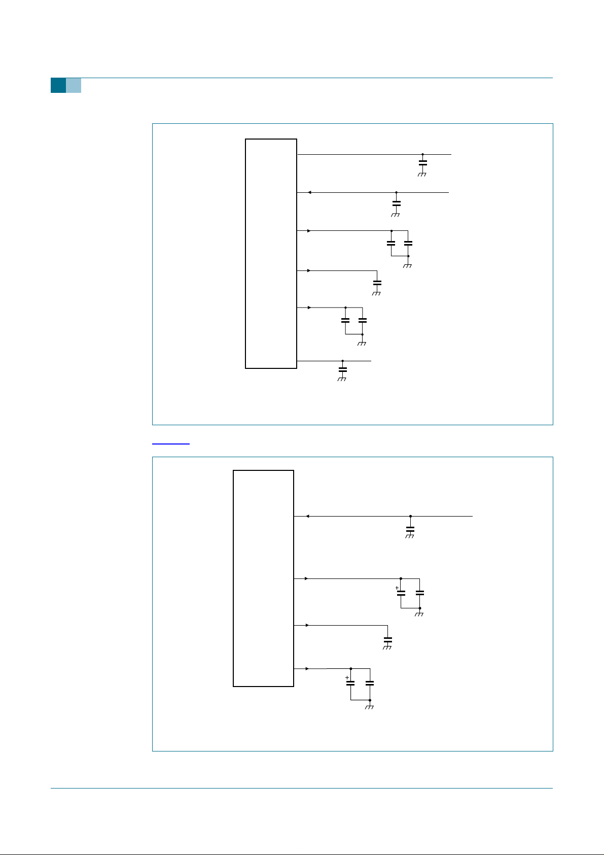
7.7 Power supply
Figure 7 shows the ISP1761 power supply connection.
9397 750 13258 © Koninklijke Philips Electronics N.V. 2005. All rights reserved.
Product data sheet Rev. 01 — 12 January 2005 26 of 158
Page 27
Philips Semiconductors
ISP1761
Hi-Speed USB OTG controller
10, 40, 48,
59, 67, 75,
83, 94,
104, 115
ISP1761
5, 50, 118
004aaa539
6, 7
126
V
CC(5V0)
V
CC(I/O)
V
REG(1V8)
85
V
REG(1V8)
V
REG(3V3)
9
V
CC(C_IN)
10 µF
+
3.3 V
100 nF
10 µF
100 nF
+
100 nF
3.3 V to 5 V
100 nF
1.65 V to 3.6 V
100 nF
100 nF
A 4.7 µFto10µF capacitor is required on any one of the pins—5, 50 and 118.
Fig 7. ISP1761 power supply connection
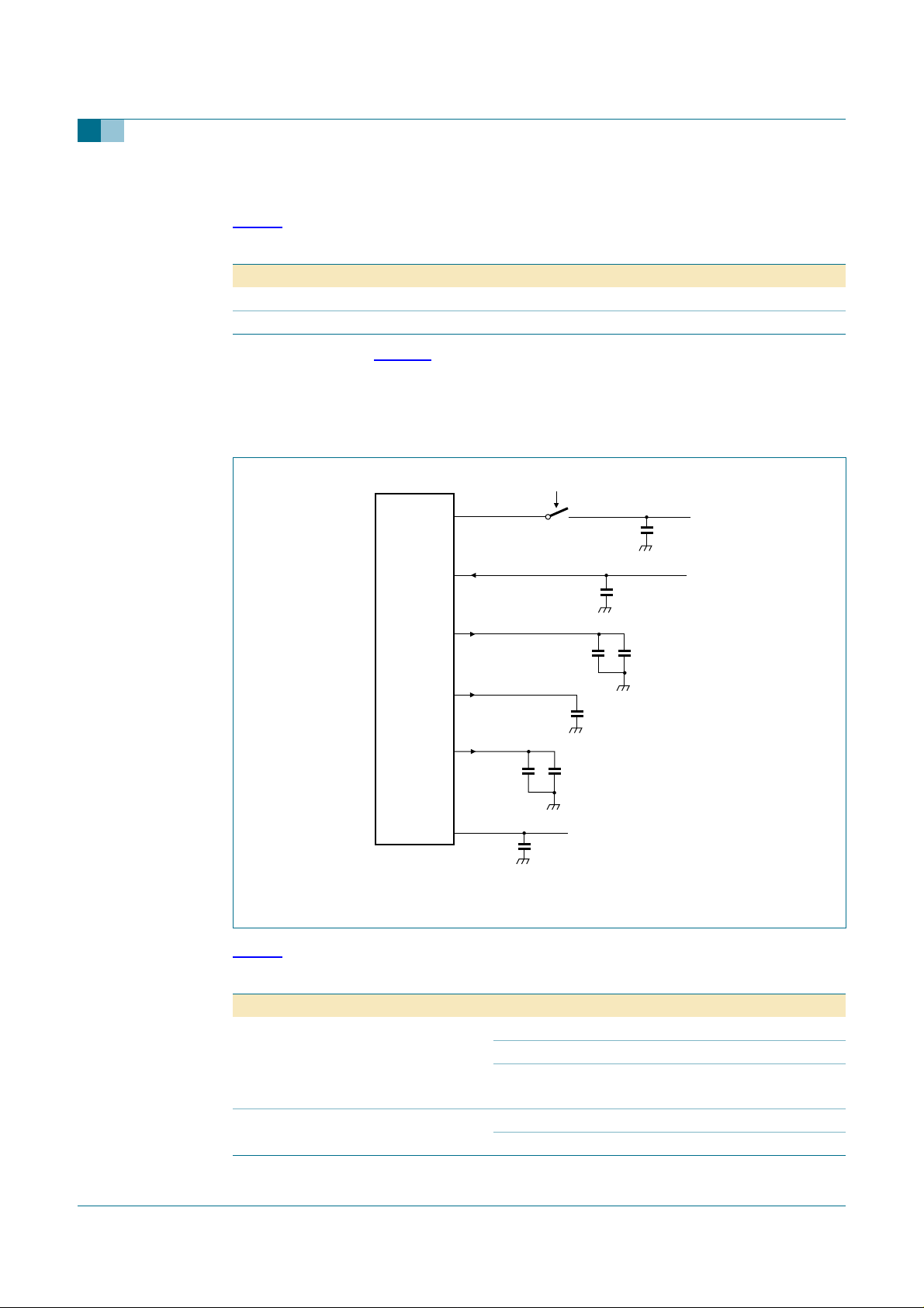
Figure 8 shows the most commonly used power supply connection.
ISP1761
6, 7, 10, 40,
48, 59, 67,
75, 83, 94,
104, 115, 126
5, 50, 118
004aaa540
V
V
85
V
V
9
CC(5V0)
REG(1V8)
REG(1V8)
REG(3V3)
V
,
10 µF
CC(I/O)
V
CC(C_IN)
,
10 µF
100 nF
A 4.7 µFto10µF capacitor is required on any one of the pins—5, 50 and 118.
Fig 8. Most commonly used power supply connection
3.3 V
100 nF
100 nF
100 nF
9397 750 13258 © Koninklijke Philips Electronics N.V. 2005. All rights reserved.
Product data sheet Rev. 01 — 12 January 2005 27 of 158
Page 28
Philips Semiconductors
7.7.1 Hybrid mode
Table 6 shows the description of hybrid mode.
Table 6: Hybrid mode
Voltage Status
V
CC(5V0)
V
CC(I/O)
ISP1761
Hi-Speed USB OTG controller
off
on
In hybrid mode (see Figure 9), V
can be switched off using an external PMOS
CC(5V0)
transistor,controlled using one of the GPIO pins of the processor. This helps to reduce the
suspend current (I
V
is off during suspend, a 2 ms reset pulse is required when power is switched
CC(5V0)
) below 100 µA. If the ISP1761 is used in hybrid mode and
CC(I/O
back to on, before starting to program the resume.
controlled by the CPU
10, 40, 48,
59, 67, 75,
83, 94,
104, 115
ISP1761
5, 50, 118
6, 7
85
9
V
CC(5V0)
V
CC(I/O)
V
REG(1V8)
V
REG(1V8)
V
REG(3V3)
10 µF
+
10 µF
100 nF
+
100 nF
3.3 V to 5 V
100 nF
1.65 V to 3.6 V
100 nF
100 nF
V
CC(C_IN)
126
004aaa676
A 4.7 µFto10µF capacitor is required on any one of the pins—5, 50 and 118.
3.3 V
100 nF
Fig 9. Hybrid mode
Table 7 shows the status of output pins during hybrid mode.
Table 7: Pin status during hybrid mode
Pins V
DATA[31:0], A[17:1], TEST, HC_IRQ,
DC_IRQ, HC_DREQ, DC_DREQ,
HC_DACK, DC_DACK,
HC_SUSPEND/WAKEUP_N,
CC(I/O)
on on normal
on off high-Z
off X undefined
DC_SUSPEND/WAKEUP_N
CS_N, RESET_N, RD_N, WR_N on X input
off X undefined
9397 750 13258 © Koninklijke Philips Electronics N.V. 2005. All rights reserved.
Product data sheet Rev. 01 — 12 January 2005 28 of 158
V
CC(5V0)
Status
Page 29
Philips Semiconductors
7.8 Overcurrent detection
The ISP1761 can implement a digital or analog overcurrent detection scheme. Bit 15 of
the HW Mode Control register can be programmed to select the analog or digital
overcurrent detection. An analog overcurrent detection circuit is integrated on-chip. The
main features of this circuit are self reporting, automatic resetting, low-trip time and low
cost. This circuit offers an easy solution at no extra hardware cost on the board. The port
power will be automatically disabled by the ISP1761 on an overcurrent event occurrence,
by deasserting the PSWn_N signal without any software intervention.
When using the integrated analog overcurrent detection, the range of the overcurrent
detection voltage for the ISP1761 is 45 mV to 90 mV. Calculation of the external
components should be based on the 45 mV value, with the actual overcurrent detection
threshold usually positioned in the middle of the interval.
ISP1761
Hi-Speed USB OTG controller
For an overcurrent limit of 500 mA per port, a PMOS transistor with R
approximately 100 mΩ is required. If a PMOS transistor with a lower R
DSON
DSON
of
is used, the
analog overcurrent detection can be adjusted using a series resistor; see Figure 10.
∆V
Fig 10. Adjusting analog overcurrent detection limit (optional)
= ∆V
PMOS
∆V
I
OC(nom)
= voltage drop on PMOS
PMOS
=1µA.
(1) Rtd is optional.
OC(TRIP)
= ∆V
5 V
TRIP(intrinsic)
REF5V
− (I
OC(nom)
ISP1761
× Rtd), where:
PSWn_N
I
OC
(1)
R
td
OCn_N
004aaa662
The digital overcurrent scheme requires using an external power switch with integrated
overcurrent detection, such as: LM3526, MIC2526 (2 ports) or LM3544 (4 ports). These
devices are controlled by PSWn_N signals corresponding to each port. In the case of
overcurrent occurrence, these devices will assert OCn_N signals. On OCn_N assertion,
the ISP1761 cuts off the port power by deasserting PSWn_N. The external integrated
power switch will also automatically cut-off the port power in the case of an overcurrent
event, by implementing a thermal shutdown. An internal delay filter of 1 ms to 3 ms will
prevent false overcurrent reporting because of in-rush currents when plugging a USB
device.
9397 750 13258 © Koninklijke Philips Electronics N.V. 2005. All rights reserved.
Product data sheet Rev. 01 — 12 January 2005 29 of 158
Page 30
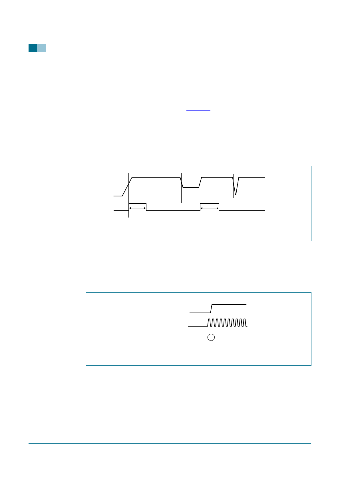
Philips Semiconductors
7.9 Power-On Reset (POR)
ISP1761
Hi-Speed USB OTG controller
When V
(t
) will be typically 800 ns. The pulse is started when V
PORP
is directly connected to the RESET_N pin, the internal POR pulse width
CC(5V0)
rises above V
CC(5V0)
TRIP
(1.2 V).
To give a better viewof the functionality, Figure 11 shows a possible curve of V
CC(5V0)
with
dips at t2–t3 and t4–t5. If the dip at t4–t5 is too short (that is, < 11 µs), the internal POR
pulse will not react and will remain LOW. The internal POR starts with a 1 at t0. At t1, the
detector will see the passing of the trip level and a delay element will add another t
PORP
before it drops to 0.
The internal POR pulse will be generated whenever V
drops below V
CC(5V0)
TRIP
for more
than 11 µs.
V
CC(5V0)
V
TRIP
t0 t1
t
PORP
(1) PORP = Power-On Reset Pulse.
Fig 11. Internal power-on reset timing
t2
t3
t
PORP
t4
t5
(1)
004aaa584
PORP
The recommended RESET input pulse length at power-on should be at least 2 ms to
ensure that internal clocks are stable.
The RESET_N pin can be either connected to V
(using the internal POR circuit) or
CC(I/O)
externally controlled (by the microcontroller, ASIC, and so on). Figure 12 shows the
availability of the clock with respect to the external POR.
RESET_N
EXTERNAL CLOCK
004aaa583
A
Stable external clock is available at A.
Fig 12. Clock with respect to the external power-on reset
9397 750 13258 © Koninklijke Philips Electronics N.V. 2005. All rights reserved.
Product data sheet Rev. 01 — 12 January 2005 30 of 158
Page 31

Philips Semiconductors
8. Host Controller
Table 8 shows the bit description of the registers.
• All registers range from 0000h to 03FFh. These registers can be read or written as
double word, that is 32-bit data.
• Operational registers range from 0000h to 01FFh. Host Controller-specific and OTG
Controller-specific registers range from 0300h to 03FFh. Peripheral
Controller-specific registers range from 0200h to 02FFh.
• 17 address lines (15/14 addresses—necessary for addressing of up to 64 kB range
on a 16-bit/32-bit data bus configuration + additional 2 addresses for bank
select/virtual segmentation for memory address access time improvement). A0 is not
defined because 8-bit access is not implemented.
Table 8: Host Controller-specific register overview
Address Register Reset value References
EHCI capability registers
0000h CAPLENGTH 20h
0002h HCIVERSION 0100h
0004h HCSPARAMS 0000 0011h
0008h HCCPARAMS 0000 0086h
EHCI operational registers
0020h USBCMD 0008 0000h
0024h USBSTS 0000 1000h
0028h USBINTR 0000 0000h
002Ch FRINDEX 0000 0000h
0030h CTRLDSSEGMENT 0000 0000h
0060h CONFIGFLAG 0000 0000h
0064h PORTSC1 0000 2000h
0130h ISO PTD Done Map 0000 0000h
0134h ISO PTD Skip Map FFFF FFFFh
0138h ISO PTD Last PTD 0000 0000h
0140h INT PTD Done Map 0000 0000h
0144h INT PTD Skip Map FFFF FFFFh
0148h INT PTD Last PTD 0000 0000h
0150h ATL PTD Done Map 0000 0000h
0154h ATL PTD Skip Map FFFF FFFFh
0158h ATL PTD Last PTD 0000 0000h
Configuration registers
0300h HW Mode Control 0000 0000h
0304h HcChipID 0001 1761h
0308h HcScratch 0000 0000h
030Ch SW Reset 0000 0000h
0330h HcDMAConfiguration 0000 0000h
0334h HcBufferStatus 0000 0000h
ISP1761
Hi-Speed USB OTG controller
Section 8.1.1 on page 32
Section 8.1.2 on page 32
Section 8.1.3 on page 32
Section 8.1.4 on page 33
Section 8.2.1 on page 34
Section 8.2.2 on page 35
Section 8.2.3 on page 36
Section 8.2.4 on page 36
Section 8.2.5 on page 37
Section 8.2.6 on page 37
Section 8.2.7 on page 38
Section 8.2.8 on page 40
Section 8.2.9 on page 40
Section 8.2.10 on page 40
Section 8.2.11 on page 41
Section 8.2.12 on page 41
Section 8.2.13 on page 41
Section 8.2.14 on page 42
Section 8.2.15 on page 42
Section 8.2.16 on page 42
Section 8.3.1 on page 42
Section 8.3.2 on page 44
Section 8.3.3 on page 44
Section 8.3.4 on page 44
Section 8.3.5 on page 45
Section 8.3.6 on page 46
9397 750 13258 © Koninklijke Philips Electronics N.V. 2005. All rights reserved.
Product data sheet Rev. 01 — 12 January 2005 31 of 158
Page 32

Philips Semiconductors
ISP1761
Hi-Speed USB OTG controller
Table 8: Host Controller-specific register overview
Address Register Reset value References
0338h ATL Done Timeout 0000 0000h Section 8.3.7 on page 47
033Ch Memory 0000 0000h
0340h Edge Interrupt Count 0000 000Fh
0344h DMA Start address 0000 0000h
0354h Power Down Control 03E8 1BA0h
Interrupt registers
0310h HcInterrupt 0000 0000h
0314h HcInterruptEnable 0000 0000h
0318h ISO IRQ Mask OR 0000 0000h
031Ch INT IRQ Mask OR 0000 0000h
0320h ATL IRQ Mask OR 0000 0000h
0324h ISO IRQ Mask AND 0000 0000h
0328h INT IRQ Mask AND 0000 0000h
032Ch ATL IRQ Mask AND 0000 0000h
8.1 EHCI capability registers
8.1.1 CAPLENGTH register (R: 0000h)
…continued
Section 8.3.8 on page 47
Section 8.3.9 on page 48
Section 8.3.10 on page 49
Section 8.3.11 on page 50
Section 8.4.1 on page 52
Section 8.4.2 on page 54
Section 8.4.3 on page 56
Section 8.4.4 on page 56
Section 8.4.5 on page 56
Section 8.4.6 on page 56
Section 8.4.7 on page 57
Section 8.4.8 on page 57
The bit description of the Capability Length (CAPLENGTH) register is given in Table 9.
Table 9: CAPLENGTH register: bit description
Bit Symbol Access Value Description
7 to 0 CAPLENGTH
[7:0]
R 20h Capability Length: This is used as an offset. It
8.1.2 HCIVERSION register (R: 0002h)
Table 10 shows the bit description of the Host Controller Interface Version Number
(HCIVERSION) register.
Table 10: HCIVERSION register: bit description
Bit Symbol Access Value Description
15 to 0 HCIVERSION[15:0] R 0100h Host Controller Interface Version Number:
8.1.3 HCSPARAMS register (R: 0004h)
The Host Controller Structural Parameters (HCSPARAMS) register is a set of fields that
are structural parameters. The bit allocation is given in Table 11.
is added to the register base to find the
beginning of the operational register space.
It contains a BCD encoding of the version
number of the interface to which the Host
Controller interface conforms.
9397 750 13258 © Koninklijke Philips Electronics N.V. 2005. All rights reserved.
Product data sheet Rev. 01 — 12 January 2005 32 of 158
Page 33

Philips Semiconductors
ISP1761
Hi-Speed USB OTG controller
Table 11: HCSPARAMS register: bit allocation
Bit 31 30 29 28 27 26 25 24
Symbol reserved
Reset 00000000
Access RRRRRRRR
Bit 23 22 21 20 19 18 17 16
Symbol DPN[3:0] reserved P_INDI
CATOR
Reset 00000000
Access RRRRRRRR
Bit 15 14 13 12 11 10 9 8
Symbol N_CC[3:0] N_PCC[3:0]
Reset 00000000
Access RRRRRRRR
Bit 7 6 5 4 3 2 1 0
Symbol PRR reserved PPC N_PORTS[3:0]
Reset 00010001
Access RRRRRRRR
Table 12: HCSPARAMS register: bit description
Bit Symbol Description
31 to 24 - reserved; write logic 0
23 to 20 DPN[3:0] Debug Port Number: This field identifies which of the Host
Controller ports is the debug port.
19 to 17 - reserved; write logic 0
16 P_INDICATOR Port Indicators: This bit indicates whether the ports support port
indicator control.
15 to 12 N_CC[3:0] Number of Companion Controller: This field indicates the number
of companion controllers associated with this Hi-Speed USB Host
Controller.
11 to 8 N_PCC[3:0] Number of Ports per Companion Controller: This field indicates
the number of ports supported per companion Host Controller.
7 PRR Port Routing Rules: This field indicates the method used for
mapping ports to the companion controllers.
6 to 5 - reserved; write logic 0
4 PPC Port Power Control: This field indicates whether the Host Controller
implementation includes port power control.
3 to 0 N_PORTS[3:0] N_Ports: This field specifies the number of physical downstream
ports implemented on this Host Controller.
[1] Fordetails on register bit description, referto
Serial Bus Rev. 1.0
.
[1]
Enhanced Host Controller Interface Specification forUniversal
8.1.4 HCCPARAMS register (R: 0008h)
The Host Controller Capability Parameters (HCCPARAMS) register is a 4 B register, and
the bit allocation is given in Table 13.
9397 750 13258 © Koninklijke Philips Electronics N.V. 2005. All rights reserved.
Product data sheet Rev. 01 — 12 January 2005 33 of 158
Page 34

Philips Semiconductors
ISP1761
Hi-Speed USB OTG controller
Table 13: HCCPARAMS register: bit allocation
Bit 31 30 29 28 27 26 25 24
Symbol reserved
Reset 00000000
Access RRRRRRRR
Bit 23 22 21 20 19 18 17 16
Symbol reserved
Reset 00000000
Access RRRRRRRR
Bit 15 14 13 12 11 10 9 8
Symbol EECP[7:0]
Reset 00000000
Access RRRRRRRR
Bit 7 6 5 4 3 2 1 0
Symbol IST[3:0] reserved ASPC PFLF 64AC
Reset 10000110
Access RRRRRRRR
Table 14: HCCPARAMS register: bit description
Bit Symbol Description
31 to 16 - reserved; write logic 0
15 to 8 EECP[7:0] EHCI Extended Capabilities Pointer: Default = implementation
dependent. This optional field indicates the existence of a capabilities list.
7 to 4 IST[3:0] Isochronous Scheduling Threshold: Default= implementation
dependent. This field indicates, relative to the current position of the
executing Host Controller, where software can reliably update the
isochronous schedule.
3 - reserved; write logic 0
2 ASPC Asynchronous Scheduling Park Capability: Default = implementation
dependent. If this bit is set to logic 1, the Host Controller supports the park
feature for high-speed queue heads in the Asynchronous Schedule.
1 PFLF Programmable Frame List Flag: Default= implementation dependent. If
this bit is cleared, the system software must use a frame list length of
1024 elements with this Host Controller.
If PFLF is set, the system software can specify and use a smaller frame
list and configure the host through the USBCMD register FLS field.
0 64AC 64-bit addressing capability: This field documents the addressing range
capability.
[1] Fordetails on register bit description, referto
Serial Bus Rev. 1.0
.
[1]
Enhanced Host Controller Interface Specification forUniversal
8.2 EHCI operational registers
8.2.1 USBCMD register (R/W: 0020h)
The USB Command (USBCMD) register indicates the command to be executed by the
serial Host Controller.Writing to this register causes a command to be executed. Table 15
shows the USBCMD register bit allocation.
9397 750 13258 © Koninklijke Philips Electronics N.V. 2005. All rights reserved.
Product data sheet Rev. 01 — 12 January 2005 34 of 158
Page 35

Philips Semiconductors
ISP1761
Hi-Speed USB OTG controller
Table 15: USBCMD register: bit allocation
Bit 31 30 29 28 27 26 25 24
Symbol reserved
Reset 00000000
Access R/W R/W R/W R/W R/W R/W R/W R/W
Bit 23 22 21 20 19 18 17 16
Symbol reserved
Reset 00001000
Access R/W R/W R/W R/W R/W R/W R/W R/W
Bit 15 14 13 12 11 10 9 8
Symbol reserved
Reset 00000000
Access R/W R/W R/W R/W R/W R/W R/W R/W
Bit 7 6 5 4 3 2 1 0
Symbol LHCR reserved
Reset 00000000
Access R/W R/W R/W R/W R/W R/W R/W R/W
[1]
[1]
[1]
[1]
RS
[1] The reserved bits should always be written with the reset value.
Table 16: USBCMD register: bit description
Bit Symbol Description
31 to 8 - reserved
7 LHCR Light Host Controller Reset (optional): If implemented, it allows the
driver software to reset the EHCI controller without affecting the state of
the ports or the relationship to the companion Host Controllers. If not
implemented, a read of this field will always return logic 0.
6 to 1 - reserved
0RSRun/Stop: 1 = Run, 0 = Stop. When set, the Host Controller executes the
schedule.
[1] Fordetails on register bit description, referto
Serial Bus Rev. 1.0
.
8.2.2 USBSTS register (R/W: 0024h)
The USB Status (USBSTS) register indicates pending interrupts and various states of the
Host Controller. The status resulting from a transaction on the serial bus is not indicated in
this register. Software clears the register bits by writing ones to them. The bit allocation is
given in Table 17.
[1]
Enhanced Host Controller Interface Specification forUniversal
9397 750 13258 © Koninklijke Philips Electronics N.V. 2005. All rights reserved.
Product data sheet Rev. 01 — 12 January 2005 35 of 158
Page 36

Philips Semiconductors
ISP1761
Hi-Speed USB OTG controller
Table 17: USBSTS register: bit allocation
Bit 31 30 29 28 27 26 25 24
Symbol reserved
Reset 00000000
Access R/W R/W R/W R/W R/W R/W R/W R/W
Bit 23 22 21 20 19 18 17 16
Symbol reserved
Reset 00000000
Access R/W R/W R/W R/W R/W R/W R/W R/W
Bit 15 14 13 12 11 10 9 8
Symbol reserved
Reset 00010000
Access R/W R/W R/W R/W R/W R/W R/W R/W
Bit 7 6 5 4 3 2 1 0
Symbol reserved
Reset 00000000
Access R/W R/W R/W R/W R/W R/W R/W R/W
[1]
[1]
[1]
[1]
FLR PCD reserved
[1]
[1] The reserved bits should always be written with the reset value.
Table 18: USBSTS register: bit description
Bit Symbol Description
31 to 4 - reserved; write logic 0
3 FLR Frame List Rollover: The Host Controller sets this bit to logic 1 when the
Frame List Index rolls over from its maximum value to zero.
2 PCD Port Change Detect: The Host Controller sets this bit to logic 1 when any
port, where the PO bit is cleared, has a change to a one or a FPR bit
changes to a one as a result of a J-K transition detected on a suspended
port.
1 to 0 - reserved
[1] Fordetails on register bit description, referto
Serial Bus Rev. 1.0
.
[1]
Enhanced Host Controller Interface Specification forUniversal
8.2.3 USBINTR register (R/W: 0028h)
All the bits in this register are reserved.
8.2.4 FRINDEX register (R/W: 002Ch)
The Frame Index (FRINDEX) register is used by the Host Controller to index into the
periodic frame list. The register updates every 125 µs (once each microframe). Bits n to 3
are used to select a particular entry in the Periodic Frame List during periodic schedule
execution. The number of bits used for the index depends on the size of the frame list as
set by the system software in the FLS (Frame List Size) field of the USBCMD register.
This register must be written as a Double Word. A Word-only write (16-bit mode) produces
undefined results. This register cannot be written unless the Host Controller is in the
halted state as indicated by the HCH (HCHalted) bit. A write to this register while the RS
(Run/Stop) bit is set produces undefined results. Writes to this register also affect the SOF
value. The bit allocation is given in Table 19.
9397 750 13258 © Koninklijke Philips Electronics N.V. 2005. All rights reserved.
Product data sheet Rev. 01 — 12 January 2005 36 of 158
Page 37

Philips Semiconductors
ISP1761
Hi-Speed USB OTG controller
Table 19: FRINDEX register: bit allocation
Bit 31 30 29 28 27 26 25 24
Symbol reserved
Reset 00000000
Access R/W R/W R/W R/W R/W R/W R/W R/W
Bit 23 22 21 20 19 18 17 16
Symbol reserved
Reset 00000000
Access R/W R/W R/W R/W R/W R/W R/W R/W
Bit 15 14 13 12 11 10 9 8
Symbol reserved
Reset 00000000
Access R/W R/W R/W R/W R/W R/W R/W R/W
Bit 7 6 5 4 3 2 1 0
Symbol FRINDEX[7:0]
Reset 00000000
Access R/W R/W R/W R/W R/W R/W R/W R/W
[1]
[1]
[1]
FRINDEX[13:8]
[1] The reserved bits should always be written with the reset value.
Table 20: FRINDEX register: bit description
Bit Symbol Description
31 to 14 - reserved
13 to 0 FRINDEX[13:0] Frame Index: Bits in this register are used for the frame number in the
SOF packet and as the index into the Frame List. The value in this
register increments at the end of each time frame (for example,
microframe).
[1] Fordetails on register bit description, referto
Serial Bus Rev. 1.0
.
8.2.5 CTRLDSSEGMENT register (R/W: 0030h)
The Control Data Structure Segment (CTRLDSSEGMENT) register corresponds to the
most significant address bits (bits 63 to 32) for all EHCI data structures. If the 64AC (64-bit
Addressing Capability) field in HCCPARAMS is cleared, then this register is not used and
software cannot write to it (reading from this register returns zero).
If the 64AC (64-bit Addressing Capability) field in HCCPARAMS is set, this register is used
with link pointers to construct 64-bit addresses to EHCI control data structures. This
register is concatenated with the link pointer from either the PERIODICLISTBASE,
ASYNCLISTADDR, or any control data structure link field to construct a 64-bit address.
[1]
Enhanced Host Controller Interface Specification forUniversal
This register allows the host software to locate all control data structures within the same
4 GB memory segment.
8.2.6 CONFIGFLAG register (R/W: 0060h)
The bit allocation of the Configure Flag (CONFIGFLAG) register is given in Table 21.
9397 750 13258 © Koninklijke Philips Electronics N.V. 2005. All rights reserved.
Product data sheet Rev. 01 — 12 January 2005 37 of 158
Page 38

Philips Semiconductors
ISP1761
Hi-Speed USB OTG controller
Table 21: CONFIGFLAG register: bit allocation
Bit 31 30 29 28 27 26 25 24
Symbol reserved
Reset 00000000
Access R/W R/W R/W R/W R/W R/W R/W R/W
Bit 23 22 21 20 19 18 17 16
Symbol reserved
Reset 00000000
Access R/W R/W R/W R/W R/W R/W R/W R/W
Bit 15 14 13 12 11 10 9 8
Symbol reserved
Reset 00000000
Access R/W R/W R/W R/W R/W R/W R/W R/W
Bit 7 6 5 4 3 2 1 0
Symbol reserved
Reset 00000000
Access R/W R/W R/W R/W R/W R/W R/W R/W
[1]
[1]
[1]
[1]
CF
[1] The reserved bits should always be written with the reset value.
Table 22: CONFIGFLAG register: bit description
Bit Symbol Description
31 to 1 - reserved
0CFConfigure Flag: The host software sets this bit as the last action when it is
configuring the Host Controller. This bit controls the default port-routing control
logic.
[1] Fordetails on register bit description, referto
Serial Bus Rev. 1.0
.
[1]
8.2.7 PORTSC1 register (R, R/W, R/WC (field dependent): 0064h)
The Port Status and Control (PORTSC) register (bit allocation: Table 23) is in the power
well. It is reset byhardware only when the auxiliary power is initially applied or in response
to a Host Controller reset. The initial conditions of a port are:
• No peripheral connected
• Port disabled.
If the port has power control, software cannot change the state of the port until it sets the
port power bits. Software must not attempt to change the state of the port until the power
is stable on the port (maximum delay is 20 ms from the transition).
Enhanced Host Controller Interface Specification forUniversal
9397 750 13258 © Koninklijke Philips Electronics N.V. 2005. All rights reserved.
Product data sheet Rev. 01 — 12 January 2005 38 of 158
Page 39

Philips Semiconductors
ISP1761
Hi-Speed USB OTG controller
Table 23: PORTSC 1 register: bit allocation
Bit 31 30 29 28 27 26 25 24
Symbol reserved
Reset 00000000
Access R/W R/W R/W R/W R/W R/W R/W R/W
Bit 23 22 21 20 19 18 17 16
Symbol reserved
[1]
Reset 00000000
Access R/W R/W R/W R/W R/W R/W R/W R/W
Bit 15 14 13 12 11 10 9 8
Symbol PIC[1:0] PO PP LS[1:0] reserved
Reset 00100000
Access R R R/W R/W R/W R/W R/W R
Bit 7 6 5 4 3 2 1 0
Symbol SUSP FPR reserved
Reset 00000000
Access R/W R/W R/W R/W R/W R/W R/W R
[1]
PTC[3:0]
[1]
[1]
PED ECSC ECCS
PR
[1] The reserved bits should always be written with the reset value.
Table 24: PORTSC 1 register: bit description
Bit Symbol Description
31 to 20 - reserved
19 to 16 PTC[3:0] Port Test Control: When this field is zero, the port is not operating in a
test mode. A non-zero value indicates that it is operating in test mode
indicated by the value.
15 to 14 PIC[1:0] Port Indicator Control: Writing to this field has no effect if the
P_INDICATOR bit in the HCSPARAMS register is logic 0.
For a description on how these bits are implemented, refer to
Serial Bus Specification Rev. 2.0
13 PO Port Owner: This bit unconditionally goes to logic 0 when the configured
bit in the CONFIGFLAG register makes a logic 0 to logic 1 transition. This
bit unconditionally goes to logic 1 whenever the configured bit is logic0.
12 PP Port Power: The function of this bit depends on the value of the PPC
(Port Power Control) field in the HCSPARAMS register.
11 to 10 LS[1:0] Line Status: This field reflect the current logical levels of the DP (bit11)
and DM (bit 10) signal lines.
9 - reserved
8PRPort Reset: Logic 1 means the port is in the reset state. Logic 0 means
the port is not in reset.
7 SUSP Suspend:Logic 1 means the port is in the suspend state. Logic 0 means
the port is not suspended.
6 FPR Force Port Resume: Logic 1 means resume detected or driven on the
port. Logic 0 means no resume (K-state) detected or driven on the
[2]
port.
5 to 3 - reserved
[1]
[2]
Universal
.
[2]
[2]
9397 750 13258 © Koninklijke Philips Electronics N.V. 2005. All rights reserved.
Product data sheet Rev. 01 — 12 January 2005 39 of 158
Page 40

Philips Semiconductors
ISP1761
Hi-Speed USB OTG controller
Table 24: PORTSC 1 register: bit description
Bit Symbol Description
2 PED Port Enabled/Disabled: Logic 1 means enable. Logic 0 means
disable.
1 ECSC Connect Status Change: Logic 1 means change in ECCS. Logic 0
means no change.
0 ECCS Current Connect Status: Logic 1 indicates a peripheral is present on
the port. Logic 0 indicates no peripheral is present.
[1] Fordetails on register bit description, referto
Serial Bus Rev. 1.0
[2] These fields read logic 0, if the PP (Port Power) bit in register PORTSC 1 is logic 0.
.
[1]
[2]
[2]
Enhanced Host Controller Interface Specification forUniversal
8.2.8 ISO PTD Done Map register (R: 0130h)
The bit description of the register is given in Table 25.
Table 25: ISO PTD Done Map register: bit description
Bit Symbol Access Value Description
31 to 0 ISO_PTD_DONE
_MAP[31:0]
This register represents a direct map of the done status of the 32 PTDs. The bit
corresponding to a certain PTD will be set to logic 1 as soon as that PTD execution is
completed. Reading the Done Map register will clear all the bits that are set to logic 1, and
the next reading will reflect the updated status of new executed PTDs.
R 0000 0000h ISO PTD Done Map: Done map for each of
…continued
[2]
the 32 PTDs for the ISO transfer
8.2.9 ISO PTD Skip Map register (R/W: 0134h)
Table 26 shows the bit description of the register.
Table 26: ISO PTD Skip Map register: bit description
Bit Symbol Access Value Description
31 to 0 ISO_PTD_SKIP_
MAP[31:0]
R/W FFFF FFFFh ISO PTD Skip Map: Skip map foreach
When a bit in the PTD Skip Map is set to logic 1 that PTD will be skipped although its V bit
may be set. The information in that PTD is not processed. For example, NextPTDPointer
will not affect the order of processing of PTDs. The Skip bit should not be normally set on
the position indicated by NextPTDPointer.
8.2.10 ISO PTD Last PTD register (R/W: 0138h)
Table 27 shows the bit description of the ISO PTD Last PTD register.
Table 27: ISO PTD Last PTD register: bit description
Bit Symbol Access Value Description
31 to 0 ISO_PTD_
LAST_
PTD[31:0]
R/W 0000 0000h ISO PTD last PTD: Last PTD of the 32 PTDs.
of the 32 PTDs for the ISO transfer
1h — One PTD in ISO
2h — Two PTDs in ISO
4h — Three PTDs in ISO.
9397 750 13258 © Koninklijke Philips Electronics N.V. 2005. All rights reserved.
Product data sheet Rev. 01 — 12 January 2005 40 of 158
Page 41

Philips Semiconductors
Once the LastPTD bit corresponding to a PTD is set, this will be the last PTD processed
(checking V = 1) in that PTD category. Subsequently,the process will restart with the first
PTD (of that group). This is useful to reduce the time in which all the PTDs (the respective
memory space) would be checked, especially if only a few PTDs are defined. The
LastPTD bit must be normally set to a higher position than any other position indicated by
the NextPTDPointer from an active PTD.
8.2.11 INT PTD Done Map register (R: 0140h)
The bit description of the register is given in Table 28.
Table 28: INT PTD Done Map register: bit description
Bit Symbol Access Value Description
31 to 0 INT_PTD_DONE_
This register represents a direct map of the done status of the 32 PTDs. The bit
corresponding to a certain PTD will be set to logic 1 as soon as that PTD execution is
completed. Reading the Done Map register will clear all the bits that are set to logic 1, and
the next reading will reflect the updated status of new executed PTDs.
MAP[31:0]
ISP1761
Hi-Speed USB OTG controller
R 0000 0000h INT PTD Done Map: Done map for
each of the 32 PTDs for the INT transfer
8.2.12 INT PTD Skip Map register (R/W: 0144h)
Table 29 shows the bit description of the INT PTD Skip Map register.
Table 29: INT PTD Skip Map register: bit description
Bit Symbol Access Value Description
31 to 0 INT_PTD_SKIP
_MAP[31:0]
R/W FFFF FFFFh INT PTD Skip Map: Skip map for each of
When a bit in the PTD Skip map is set to logic 1 that PTD will be skipped although its V bit
may be set. The information in that PTD is not processed. For example, NextPTDPointer
will not affect the order of processing of PTDs. The Skip bit should not be normally set on
the position indicated by NextPTDPointer.
8.2.13 INT PTD Last PTD register (R/W: 0148h)
The bit description of the register is given in Table 30.
Table 30: INT PTD Last PTD register: bit description
Bit Symbol Access Value Description
31 to 0 INT_PTD_
LAST_
PTD[31:0]
R/W 0000 0000h INT PTD Last PTD: Last PTD of the 32 PTDs.
the 32 PTDs for the INT transfer
1h — One PTD in INT
2h — Two PTDs in INT
3h — Three PTDs in INT.
Once the LastPTD bit corresponding to a PTD is set, this will be the last PTD processed
(checking V = 1) in that PTD category. Subsequently,the process will restart with the first
PTD (of that group). This is useful to reduce the time in which all the PTDs (the respective
memory space) would be checked, especially if only a few PTDs are defined. The
LastPTD bit must be normally set to a higher position than any other position indicated by
the NextPTDPointer from an active PTD.
9397 750 13258 © Koninklijke Philips Electronics N.V. 2005. All rights reserved.
Product data sheet Rev. 01 — 12 January 2005 41 of 158
Page 42

Philips Semiconductors
8.2.14 ATL PTD Done Map register (R: 0150h)
Table 31 shows the bit description of the ATL PTD Done Map register.
Table 31: ATL PTD Done Map register: bit description
Bit Symbol Access Value Description
31 to 0 ATL_PTD_DONE_
This register represents a direct map of the done status of the 32 PTDs. The bit
corresponding to a certain PTD will be set to logic 1 as soon as that PTD execution is
completed. Reading the Done Map register will clear all the bits that are set to logic 1, and
the next reading will reflect the updated status of new executed PTDs.
8.2.15 ATL PTD Skip Map register (R/W: 0154h)
The bit description of the register is given in Table 32.
Table 32: ATL PTD Skip Map register: bit description
Bit Symbol Access Value Description
31 to 0 ATL_PTD_SKIP_
MAP[31:0]
MAP[31:0]
ISP1761
Hi-Speed USB OTG controller
R 0000 0000h ATL PTD Done Map: Done map for
each of the 32 PTDs for the ATL transfer
R/W FFFF FFFFh ATL PTD Skip Map: Skip map for each
of the 32 PTDs for the ATL transfer
When a bit in the PTD Skip map is set to logic 1 that PTD will be skipped although its V bit
may be set. The information in that PTD is not processed. For example, NextPTDPointer
will not affect the order of processing of PTDs. The Skip bit should not be normally set on
the position indicated by NextPTDPointer.
8.2.16 ATL PTD Last PTD register (R/W: 0158h)
The bit description of the ATL PTD Last PTD register is given in Table 33.
Table 33: ATL PTD Last PTD register: bit description
Bit Symbol Access Value Description
31 to 0 ATL_PTD_
LAST_
PTD[31:0]
R/W 0000 0000h ATL PTD Last PTD: Last PTD of the 32 PTDs.
Once the LastPTD bit corresponding to a PTD is set, this will be the last PTD processed
(checking V = 1) in that PTD category. Subsequently,the process will restart with the first
PTD (of that group). This is useful to reduce the time in which all the PTDs (the respective
memory space) would be checked, especially if only a few PTDs are defined. The
LastPTD bit must be normally set to a higher position than any other position indicated by
the NextPTDPointer from an active PTD.
8.3 Configuration registers
1h — One PTD in ATL
2h — Two PTDs in ATL
4h — Three PTDs in ATL.
8.3.1 HW Mode Control register (R/W: 0300h)
Table 34 shows the bit allocation of the register.
9397 750 13258 © Koninklijke Philips Electronics N.V. 2005. All rights reserved.
Product data sheet Rev. 01 — 12 January 2005 42 of 158
Page 43

Philips Semiconductors
ISP1761
Hi-Speed USB OTG controller
Table 34: HW Mode Control register: bit allocation
Bit 31 30 29 28 27 26 25 24
[1]
DEV_
DMA
[1]
[1]
COMN_
IRQ
INTR_POL INTR_
COMN_
DMA
LEVEL
DATA_BUS
_WIDTH
GLOBAL_
INTR_EN
Symbol ALL_ATX_
reserved
RESET
Reset 00000000
Access R/W R/W R/W R/W R/W R/W R/W R/W
Bit 23 22 21 20 19 18 17 16
Symbol reserved
Reset 00000000
Access R/W R/W R/W R/W R/W R/W R/W R/W
Bit 15 14 13 12 11 10 9 8
Symbol ANA_DIGI
reserved
[1]
_OC
Reset 00000001
Access R/W R/W R/W R/W R/W R/W R/W R/W
Bit 7 6 5 4 3 2 1 0
Symbol reserved DACK_
POL
DREQ_
POL
reserved
Reset 00000000
Access R/W R/W R/W R/W R/W R/W R/W R/W
[1] The reserved bits should always be written with the reset value.
Table 35: HW Mode Control register: bit description
Bit Symbol Description
31 ALL_ATX_
RESET
All ATX Reset: For debugging purposes (not used normally).
1 — Enable reset, then write back logic 0
0 — No reset.
30 to 16 - reserved; write logic 0
15 ANA_DIGI_OC Analog Digital Overcurrent: This bit selects analog or digital
overcurrent detection on pins OC1_N/V
, OC2_N and OC3_N.
BUS
0 — Digital overcurrent
1 — Analog overcurrent.
14 to 12 - reserved; write logic 0
11 DEV_DMA Device DMA: When this bit and bit 9 are set, DC_DREQ and
DC_DACK peripheral signals are selected on the HC_DREQ and
HC_DACK pins
10 COMN_INT Common IRQ: When this bit is set, DC_IRQ will be generated on the
HC_IRQ pin.
9 COMN_DMA Common DMA: When this bit and bit 11 are set, the DC_DREQ and
DC_DACK peripheral signals are routed to the HC_DREQ and
HC_DACK pins.
8 DATA_BUS_
WIDTH
Data Bus Width:
0 — defines a 16-bit data bus width
1 — sets a 32-bit data bus width.
Remark: Setting this bit will affect all the controllers on the chip (Host
Controller, Peripheral Controller and OTG Controller).
9397 750 13258 © Koninklijke Philips Electronics N.V. 2005. All rights reserved.
Product data sheet Rev. 01 — 12 January 2005 43 of 158
Page 44

Philips Semiconductors
ISP1761
Hi-Speed USB OTG controller
Table 35: HW Mode Control register: bit description
Bit Symbol Description
7 - reserved; write logic 0
6 DACK_POL DACK Polarity:
1 — indicates that the DACK input is active HIGH
0 — indicates active LOW.
5 DREQ_POL DREQ Polarity:
1 — indicates that the DREQ output is active HIGH
0 — indicates active LOW.
4 to 3 - reserved; write logic 0
2 INTR_POL Interrupt Polarity:
0 — active LOW
1 — active HIGH.
1 INTR_LEVEL Interrupt Level:
0 — INT level triggered
1 — INT is edge triggered. A pulse of certain width is generated.
0 GLOBAL_INTR
_EN
Global Interrupt Enable: This bit must be set to logic 1 to enable IRQ
signal assertion.
0 — IRQ assertion disabled. IRQ will never be asserted, regardless of
other settings or IRQ events
1 — IRQ assertion enabled. IRQ will be asserted according to the
HcInterruptEnable register, and events setting and occurrence
…continued
8.3.2 HcChipID register (R: 0304h)
Read this register to get the ID of the ISP1761. This upper word of the register contains
the hardware version number and the lower word contains the chip ID. Table 36 shows the
bit description of the register.
Table 36: HcChipID register: bit description
Bit Symbol Access Value Description
31 to 0 CHIPID
[31:0]
R 0001 1761h Chip ID: This register represents the hardware
8.3.3 HcScratch register (R/W: 0308h)
This register is for testing and debugging purposes only.The value read back must be the
same as the value that was written. The bit description of this register is given in Table 37.
Table 37: HcScratch register: bit description
Bit Symbol Access Value Description
31 to 0 SCRATCH[31:0] R/W 0000 0000h Scratch: For testing and debugging
8.3.4 SW Reset register (R/W: 030Ch)
Table 38 shows the bit allocation of the register.
version number (0001h) and the chip ID (1761h)
for the Host Controller.
purposes
9397 750 13258 © Koninklijke Philips Electronics N.V. 2005. All rights reserved.
Product data sheet Rev. 01 — 12 January 2005 44 of 158
Page 45

Philips Semiconductors
ISP1761
Hi-Speed USB OTG controller
Table 38: SW Reset register: bit allocation
Bit 31 30 29 28 27 26 25 24
Symbol reserved
Reset 00000000
Access R/W R/W R/W R/W R/W R/W R/W R/W
Bit 23 22 21 20 19 18 17 16
Symbol reserved
Reset 00000000
Access R/W R/W R/W R/W R/W R/W R/W R/W
Bit 15 14 13 12 11 10 9 8
Symbol reserved
Reset 00000000
Access R/W R/W R/W R/W R/W R/W R/W R/W
Bit 7 6 5 4 3 2 1 0
Symbol reserved
Reset 00000000
Access R/W R/W R/W R/W R/W R/W R/W R/W
[1]
[1]
[1]
[1]
RESET_HCRESET_
ALL
[1] The reserved bits should always be written with the reset value.
Table 39: SW Reset register: bit description
Bit Symbol Description
31 to 2 - reserved; write logic 0
1 RESET_HC Reset Host Controller: Reset only the Host Controller-specific
registers (only registers with address below 300h).
0 — No reset
1 — Enable reset.
0 RESET_ALL Reset All: Reset all the Host Controller and CPU interface registers.
0 — No reset
1 — Enable reset.
8.3.5 HcDMAConfiguration register (R/W: 0330h)
The bit allocation of the HcDMAConfiguration register is given in Table 40.
Table 40: HcDMAConfiguration register: bit allocation
Bit 31 30 29 28 27 26 25 24
Symbol DMA_COUNTER[23:16]
Reset 00000000
Access R/W R/W R/W R/W R/W R/W R/W R/W
Bit 23 22 21 20 19 18 17 16
Symbol DMA_COUNTER[15:8]
Reset 00000000
Access R/W R/W R/W R/W R/W R/W R/W R/W
9397 750 13258 © Koninklijke Philips Electronics N.V. 2005. All rights reserved.
Product data sheet Rev. 01 — 12 January 2005 45 of 158
Page 46

Philips Semiconductors
ISP1761
Hi-Speed USB OTG controller
Bit 15 14 13 12 11 10 9 8
Symbol DMA_COUNTER[7:0]
Reset 00000000
Access R/W R/W R/W R/W R/W R/W R/W R/W
Bit 7 6 5 4 3 2 1 0
Symbol reserved
Reset 00000000
Access R/W R/W R/W R/W R/W R/W R/W R/W
[1] The reserved bits should always be written with the reset value.
Table 41: HcDMAConfiguration register: bit description
Bit Symbol Description
31 to 8 DMA_
COUNTER
[23:0]
7 to 4 - reserved
3 to 2 BURST_LEN
[1:0]
1 ENABLE_DMA Enable DMA:
0 DMA_READ_
WRITE_SEL
[1]
DMA Counter: The number of bytes to be transferred (read or write).
Remark: Different number of bursts will be generated for the same
transfer length programmed in 16-bit and 32-bit modes because
DMA_COUNTER is in number of bytes.
DMA Burst Length:
00 — Single DMA burst
01 — 4-cycle DMA burst
10 — 8-cycle DMA burst
11 — 16-cycle DMA burst.
0 — Terminate DMA
1 — Enable DMA.
DMA Read or Write Select: Indicates if the DMA operation is a write
or read (to or from the ISP1761).
0 — DMA write to the ISP1761 internal RAM is set
1 — DMA read from the ISP1761 internal RAM.
BURST_LEN[1:0] ENABLE_
DMA
DMA_READ
_WRITE_
SEL
8.3.6 HcBufferStatus register (R/W: 0334h)
Table 42 shows the bit allocation of the HcBufferStatus register.
Table 42: HcBufferStatus register: bit allocation
Bit 31 30 29 28 27 26 25 24
Symbol reserved
Reset 00000000
Access R/W R/W R/W R/W R/W R/W R/W R/W
Bit 23 22 21 20 19 18 17 16
Symbol reserved
Reset 00000000
Access R/W R/W R/W R/W R/W R/W R/W R/W
9397 750 13258 © Koninklijke Philips Electronics N.V. 2005. All rights reserved.
Product data sheet Rev. 01 — 12 January 2005 46 of 158
[1]
[1]
Page 47

Philips Semiconductors
ISP1761
Hi-Speed USB OTG controller
Bit 15 14 13 12 11 10 9 8
Symbol reserved
Reset 00000000
Access R/W R/W R/W R/W R/W R/W R/W R/W
Bit 7 6 5 4 3 2 1 0
Symbol reserved
Reset 00000000
Access R/W R/W R/W R/W R/W R/W R/W R/W
[1] The reserved bits should always be written with the reset value.
Table 43: HcBufferStatus register: bit description
Bit Symbol Description
31 to 3 - reserved
2 ISO_BUF_
FILL
1 INT_BUF_
FILL
0 ATL_BUF_
FILL
[1]
ISO Buffer Filled:
1 — Indicates one of the ISO PTDs is filled, and the ISO PTD area will
be processed
0 — Indicates there is no PTD in this area. Therefore, processing of
the ISO PTDs will be completely skipped.
INT Buffer Filled:
1 — Indicates one of the INT PTDs is filled, and the INT PTD area will
be processed
0 — Indicates there is no PTD in this area. Therefore, processing of
the INT PTDs will be completely skipped.
ATL Buffer Filled:
1 — Indicates one of the ATL PTDs is filled, and the ATL PTD area will
be processed
0 — Indicates there is no PTD in this area. Therefore, processing of
the ATL PTDs will be completely skipped.
[1]
ISO_BUF_
FILL
INT_BUF_
FILL
ATL_BUF_
FILL
8.3.7 ATL Done Timeout register (R/W: 0338h)
The bit description of the ATL Done Timeout register is given in Table 44.
Table 44: ATL Done Timeout register: bit description
Bit Symbol Access Value Description
31 to 0 ATL_DONE_
TIMEOUT
[31:0]
R/W 0000 0000h ATL Done Timeout: This register determines the
ATL done timeout interrupt. This register defines
the timeout in ms after which the ISP1761 asserts
the INT line, if enabled. It is applicable to the ATL
done PTDs only.
8.3.8 Memory register (R/W: 033Ch)
The Memory register contains the base memory read address and the respective bank.
This register needs to be set only before a first memory read cycle. Once written, the
address will be latched for the bank and will be incremented for every read of that bank
until a new address for that bank is written to change the address pointer.
The bit description of the register is given in Table 45.
9397 750 13258 © Koninklijke Philips Electronics N.V. 2005. All rights reserved.
Product data sheet Rev. 01 — 12 January 2005 47 of 158
Page 48

Philips Semiconductors
ISP1761
Hi-Speed USB OTG controller
Table 45: Memory register: bit allocation
Bit 31 30 29 28 27 26 25 24
Symbol reserved
Reset 00000000
Access R/W R/W R/W R/W R/W R/W R/W R/W
Bit 23 22 21 20 19 18 17 16
Symbol reserved
Reset 00000000
Access R/W R/W R/W R/W R/W R/W R/W R/W
Bit 15 14 13 12 11 10 9 8
Symbol START_ADDR_MEM_READ[15:8]
Reset 00000000
Access R/W R/W R/W R/W R/W R/W R/W R/W
Bit 7 6 5 4 3 2 1 0
Symbol START_ADDR_MEM_READ[7:0]
Reset 00000000
Access R/W R/W R/W R/W R/W R/W R/W R/W
[1]
[1]
MEM_BANK_SEL[1:0]
[1] The reserved bits should always be written with the reset value.
Table 46: Memory register: bit description
Bit Symbol Description
31 to 18 - reserved
17 to 16 MEM_BANK_
SEL[1:0]
15 to 0 START_
ADDR_MEM_
READ[15:0]
Memory Bank Select: Up to four memory banks can be selected. For
details on internal memory read description, see
Applicable to PIO mode memory read or write data transfers only.
Start Address for Memory Read Cycles: The start address for a
series of memory read cycles at incremental addresses in a contiguous
space. Applicable to PIO mode memory read data transfers only.
Section 7.3.1.
8.3.9 Edge Interrupt Count register (R/W: 0340h)
Table 47 shows the bit allocation of the register.
Table 47: Edge Interrupt Count register: bit allocation
Bit 31 30 29 28 27 26 25 24
Symbol MIN_WIDTH[7:0]
Reset 00000000
Access R/W R/W R/W R/W R/W R/W R/W R/W
Bit 23 22 21 20 19 18 17 16
Symbol reserved
Reset 00000000
Access R/W R/W R/W R/W R/W R/W R/W R/W
[1]
9397 750 13258 © Koninklijke Philips Electronics N.V. 2005. All rights reserved.
Product data sheet Rev. 01 — 12 January 2005 48 of 158
Page 49

Philips Semiconductors
ISP1761
Hi-Speed USB OTG controller
Bit 15 14 13 12 11 10 9 8
Symbol NO_OF_CLK[15:8]
Reset 00000000
Access R/W R/W R/W R/W R/W R/W R/W R/W
Bit 7 6 5 4 3 2 1 0
Symbol NO_OF_CLK[7:0]
Reset 00001111
Access R/W R/W R/W R/W R/W R/W R/W R/W
[1] The reserved bits should always be written with the reset value.
Table 48: Edge Interrupt Count register: bit description
Bit Symbol Description
31 to 24 MIN_
WIDTH[7:0]
23 to 16 - reserved
15 to 0 NO_OF_
CLK[15:0]
Minimum Width: Indicates the minimum width between two edge
interrupts in µSOFs (1 µSOF = 125 µs). This is not valid for level
interrupts. A count of zeromeans that interrupts occur as and when an
event occurs.
Number of Clocks: Count in number of clocks that the edge interrupt
must be kept asserted on the interface.16 clocks of 60 MHz on POR if
this register has a value of 0000h. The default IRQ pulse width is
approximately 500 ns.
8.3.10 DMA Start Address register (W: 0344h)
This register defines the start address select for the DMA read and write operations. See
Table 49 for bit allocation.
Table 49: DMA Start Address register: bit allocation
Bit 31 30 29 28 27 26 25 24
Symbol reserved
Reset 00000000
Access WWWWWWWW
Bit 23 22 21 20 19 18 17 16
Symbol reserved
Reset 00000000
Access WWWWWWWW
Bit 15 14 13 12 11 10 9 8
Symbol START_ADDR_DMA[15:8]
Reset 00000000
Access WWWWWWWW
Bit 7 6 5 4 3 2 1 0
Symbol START_ADDR_DMA[7:0]
Reset 00000000
Access WWWWWWWW
[1]
[1]
[1] The reserved bits should always be written with the reset value.
9397 750 13258 © Koninklijke Philips Electronics N.V. 2005. All rights reserved.
Product data sheet Rev. 01 — 12 January 2005 49 of 158
Page 50

Philips Semiconductors
ISP1761
Hi-Speed USB OTG controller
Table 50: DMA Start Address register: bit description
Bit Symbol Description
31 to 16 - reserved
15 to 0 START_ADDR
_DMA[15:0]
Start Address for DMA: The start address for DMA read or write
cycles.
8.3.11 Power Down Control register (R/W: 0354h)
This register is used to turn off power to the internal blocks of the ISP1761 to obtain
maximum power savings. Table 51 shows the bit allocation of the register.
Table 51: Power Down Control register: bit allocation
Bit 31 30 29 28 27 26 25 24
Symbol CLK_OFF_COUNTER[15:8]
Reset 00000011
Access R/W R/W R/W R/W R/W R/W R/W R/W
Bit 23 22 21 20 19 18 17 16
Symbol CLK_OFF_COUNTER[7:0]
Reset 11101000
Access R/W R/W R/W R/W R/W R/W R/W R/W
Bit 15 14 13 12 11 10 9 8
Symbol reserved
Reset 00011011
Access R/W R/W R/W R/W R/W R/W R/W R/W
Bit 7 6 5 4 3 2 1 0
Symbol reserved
Reset 10100000
Access R/W R/W R/W R/W R/W R/W R/W R/W
[1]
[1]
BIASEN VREG_ON OC3_PWR OC2_PWR OC1_PWR HC_CLK_
PORT3_
PD
PORT2_PDVBATDET_
PWR
reserved
[1]
EN
[1] The reserved bits should always be written with the reset value.
9397 750 13258 © Koninklijke Philips Electronics N.V. 2005. All rights reserved.
Product data sheet Rev. 01 — 12 January 2005 50 of 158
Page 51

Philips Semiconductors
Table 52: Power Down Control register: bit description
[1]
Bit
31 to 16 CLK_OFF_
15 to 13 - reserved
12 PORT3_
11 PORT2_
10 VBATDET_
9 to 6 - reserved; write logic 0
5 BIASEN BIAS Circuits Powered: Controls the power to internal BIAS circuits.
4 VREG_ON
3 OC3_PWR OC3_N Powered: Controls the powering of the overcurrent detection
Symbol Description
Clock Off Counter: Determines the wake-up status duration after any
COUNTER
[15:0]
wake-up event before the ISP1761 goes back into suspend mode.
This timeout is applicable only if, during the given interval, the Host
Controller is not programmed back to normal functionality.
03E8h — The default value. It determines the defaultwake-up interval
of 10 ms. A value of zero implies that the Host Controller neverwakes
up on any of the events. This may be useful when using the ISP1761
as a peripheral to save power by permanently programming the Host
Controller in suspend.
FFFFh — The maximum value. It determines a maximum wake-up
time of 500 ms.
The setting of this register is based on the 100 kHz ± 40 % LazyClock
frequency. It is a multiple of 10 µs period. In 16-bit mode, a write
operation to these bits with any value will determine a fixed wake-up
time of 50 ms.
Port 3 Pull-Down: Controls port 3 pull-down resistors.
PD
0 — Port 3 pull-down resistors are connected in suspend
1 — Port 3 pull-down resistors are not connected in suspend.
Port 2 Pull-Down: Controls port 2 pull-down resistors.
PD
0 — Port 2 internal pull-down resistors are connected in suspend
1 — Port 2 internal pull-down resistors are not connected in suspend.
V
Detector Powered: Controls the power to the V
PWR
BAT
0 — V
1 — V
detector is powered or enabled in suspend
BAT
detector is not powered or disabled in suspend.
BAT
0 — Internal BIAS circuits are not powered in suspend
1 — Internal BIAS circuits are powered in suspend.
Powered: Enables or disables the internal 3.3 V and 1.8 V
V
REG
regulators when the ISP1761 is in suspend.
0 — Internal regulators are powered in suspend
1 — Internal regulators are not powered in suspend.
circuitry for port 3.
0 — Overcurrent detection is powered on or enabled during suspend
1 — Overcurrent detection is powered off or disabled during suspend.
This may be useful when connecting a faulty device while the system
is in standby.
ISP1761
Hi-Speed USB OTG controller
detector.
BAT
9397 750 13258 © Koninklijke Philips Electronics N.V. 2005. All rights reserved.
Product data sheet Rev. 01 — 12 January 2005 51 of 158
Page 52

Philips Semiconductors
ISP1761
Hi-Speed USB OTG controller
Table 52: Power Down Control register: bit description
[1]
Bit
2 OC2_PWR OC2_N Powered: Controls the powering of the overcurrent detection
1 OC1_PWR OC1_N Powered: Controls the powering of the overcurrent detection
0 HC_CLK_ENHost Controller Clock Enabled: Controls internal clocks during
[1] For a 32-bit operation, the default wake-up counter value is 10 µs. For a 16-bit operation, the wake-up
counter value is 50 ms. In the 16-bit operation, read and write back the same value on initialization.
Symbol Description
circuitry for port 2.
0 — Overcurrent detection is powered on or enabled during suspend
1 — Overcurrent detection is powered off or disabled during suspend.
This may be useful when connecting a faulty device while the system
is in standby.
circuitry for port 1.
0 — Overcurrent detection is powered on or enabled during suspend
1 — Overcurrent detection is powered off or disabled during suspend.
This may be useful when connecting a faulty device while the system
is in standby.
suspend.
0 — Clocks are disabled during suspend. This is the default value.
Only the LazyClock of 100 kHz ± 40 % will be left running in suspend if
this bit is logic 0. If clocks are stopped during suspend, CLKREADY
IRQ will be generated when all clocks are running stable.
1 — All clocks are enabled even in suspend.
…continued
8.4 Interrupt registers
8.4.1 HcInterrupt register (R/W: 0310h)
The bits of this register indicate the interrupt source, defining the events that determined
the INT generation. Clearing the bits that were set because of the eventslisted is done by
writing back logic 1 to the respective position. All bits must be reset before enabling new
interrupt events.These bits will be set, regardless of the setting of bit GLOBAL_INTR_EN
in the HW Mode Control register. Table 53 shows the bit allocation of the HcInterrupt
register.
Table 53: HcInterrupt register: bit allocation
Bit 31 30 29 28 27 26 25 24
Symbol reserved
Reset 00000000
Access R/W R/W R/W R/W R/W R/W R/W R/W
Bit 23 22 21 20 19 18 17 16
Symbol reserved
Reset 00000000
Access R/W R/W R/W R/W R/W R/W R/W R/W
Bit 15 14 13 12 11 10 9 8
Symbol reserved
Reset 00000000
Access R/W R/W R/W R/W R/W R/W R/W R/W
[1]
[1]
[1]
OTG_IRQ ISO_IRQ ATL_IRQ
9397 750 13258 © Koninklijke Philips Electronics N.V. 2005. All rights reserved.
Product data sheet Rev. 01 — 12 January 2005 52 of 158
Page 53

Philips Semiconductors
ISP1761
Hi-Speed USB OTG controller
Bit 7 6 5 4 3 2 1 0
[1]
Symbol INT_IRQ CLK
READY
Reset 00000000
Access R/W R/W R/W R/W R/W R/W R/W R/W
[1] The reserved bits should always be written with the reset value.
Table 54: HcInterrupt register: bit description
Bit Symbol Description
31 to 11 - reserved; write logic 0
10 OTG_IRQ OTG_IRQ: Indicates that IRQ was asserted because of events present in
9 ISO_IRQ ISO IRQ: Indicates that IRQ was asserted because an ISO PTD was
8 ATL_IRQ ATL IRQ: Indicates that an IRQ was asserted because an ATL PTD was
7 INT_IRQ INT IRQ: Indicates that an IRQ was asserted because an INT PTD was
6 CLKREADY Clock Ready: Indicates that IRQ was asserted as the internal clock
HCSUSP reserved
the OTG Interrupt Latch register.
0 — No IRQ was asserted
1 — IRQ was asserted.
For details, see
completed, or the PTDs corresponding to the bits set in the ISO IRQ
Mask AND or ISO IRQ Mask OR register bits combination were
completed.
0 — No IRQ assertion determined by the completion of ISO PTDs
1 — IRQ asserted because of completing ISO PTDs.
For details, see
completed, or the PTDs corresponding to the bits set in the ATL IRQ
Mask AND or ATL IRQ Mask OR register bits combination were
completed.
0 — No IRQ assertion determined by the completion of ATL PTDs
1 — IRQ asserted because of completing ATL PTD.
For details, see
completed, or the PTDs corresponding to the bits set in the INT IRQ
Mask AND or INT IRQ Mask OR register bits combination were
completed.
0 — No IRQ assertion determined by the completion of INT PTDs
1 — IRQ asserted because of completing INT PTD.
For details, see
signals are running stable. Useful after a power-on or wake-up cycle.
0 — No CLKREADY event has occurred
1 — IRQ generated because of a CLKREADY event.
DMA
EOTINT
Section 7.4.
Section 7.4.
Section 7.4.
Section 7.4.
reserved
[1]
SOFITLINT
9397 750 13258 © Koninklijke Philips Electronics N.V. 2005. All rights reserved.
Product data sheet Rev. 01 — 12 January 2005 53 of 158
Page 54

Philips Semiconductors
ISP1761
Hi-Speed USB OTG controller
Table 54: HcInterrupt register: bit description
Bit Symbol Description
5 HCSUSP Host Controller Suspend: Indicates that the Host Controller has
entered suspend mode.
0 — No IRQ generated because of the Host Controller entering suspend
mode
1 — IRQ generated because of the Host Controller entering suspend
mode
If the Interrupt Service Routine (ISR) accesses the ISP1761, it will wake
up for the time specified in bits 31 to 16 of the Power Down Control
register.
4 - reserved; write logic 0
3 DMAEOT
INT
2 to 1 - reserved; write logic 0
0 SOFITLINT SOT ITL Interrupt:
DMA EOT Interrupt: Indicates DMA transfer completion.
0 — DMA transfer is not complete
1 — IRQ asserted because the DMA transfer is complete.
0 — No SOF event has occurred
1 — An SOF event has occurred.
…continued
8.4.2 HcInterruptEnable register (R/W: 0314h)
This register allows enabling or disabling of the IRQ generation because of various events
as described in Table 55.
Table 55: HcInterruptEnable register: bit allocation
Bit 31 30 29 28 27 26 25 24
[1]
[1]
[1]
DMAEOT
INT _E
OTG_IRQ_EISO_IRQ_EATL_IRQ
_E
reserved
[1]
SOFITLINT
_E
Symbol reserved
Reset 00000000
Access R/W R/W R/W R/W R/W R/W R/W R/W
Bit 23 22 21 20 19 18 17 16
Symbol reserved
Reset 00000000
Access R/W R/W R/W R/W R/W R/W R/W R/W
Bit 15 14 13 12 11 10 9 8
Symbol reserved
Reset 00000000
Access R/W R/W R/W R/W R/W R/W R/W R/W
Bit 7 6 5 4 3 2 1 0
Symbol INT_IRQ_E CLK
READY _E
Reset 00000000
Access R/W R/W R/W R/W R/W R/W R/W R/W
[1] The reserved bits should always be written with the reset value.
HCSUSP_Ereserved
[1]
9397 750 13258 © Koninklijke Philips Electronics N.V. 2005. All rights reserved.
Product data sheet Rev. 01 — 12 January 2005 54 of 158
Page 55

Philips Semiconductors
Table 56: HcInterruptEnable register: bit description
Bit Symbol Description
31 to 11 - reserved; write logic 0
10 OTG_IRQ_E OTG_IRQ Enable: Controls the IRQ assertion because of events
9 ISO_IRQ_E ISO IRQ Enable: Controls the IRQ assertion because of completing
8 ATL_IRQ_E ATL IRQ Enable: Controls the IRQ assertion because of completing
7 INT_IRQ_E INT IRQ Enable: Controls the IRQ assertion because of completing
6 CLKREADY_E Clock Ready Enable: Enables the IRQ assertion when internal clock
5 HCSUSP_E Host Controller Suspend Enable: Enables the IRQ generation when
4 - reserved; write logic 0
3 DMAEOT
2 to 1 - reserved; write logic 0
0 SOFITLINT_E SOT ITL Interrupt Enable: Controls the IRQ generation at every SOF
INT_E
ISP1761
Hi-Speed USB OTG controller
present in the OTG Interrupt Latch register.
0 — No IRQ will be asserted
1 — IRQ will be asserted.
For details, see
one or more ISO PTDs matching the ISO IRQ Mask AND or
ISO IRQ Mask OR register bits combination.
0 — No IRQ will be asserted because of completing ISO PTDs
1 — IRQ will be asserted.
For details, see
one or more ATL PTDs matching the ATL IRQ Mask AND or
ATL IRQ Mask OR register bits combination.
0 — No IRQ will be asserted because of completing ATL PTDs
1 — IRQ will be asserted.
For details, see
one or more INT PTDs matching the INT IRQ Mask AND or
INT IRQ Mask OR register bits combination.
0 — No IRQ will be asserted because of completing INT PTDs
1 — IRQ will be asserted.
For details, see
signals are running stable. Useful after power-on or wake-up.
0 — No IRQ will be generated after a CLKREADY_E event has
occurred
1 — IRQ will be generated after a CLKREADY_E event.
the Host Controller enters suspend mode.
0 — No IRQ will be generated because of the Host Controller entering
suspend mode
1 — IRQ will be generated at the Host Controller entering suspend
mode.
DMA EOT Interrupt Enable: Controls assertion of IRQ on the DMA
transfer completion.
0 — No IRQ will be generated after the DMA transfer is completed
1 — IRQ will be asserted because of the DMA transfer completion.
occurrence.
0 — No IRQ will be generated on an SOF occurrence
1 — IRQ will be asserted at every SOF.
Section 7.4.
Section 7.4.
Section 7.4.
Section 7.4.
9397 750 13258 © Koninklijke Philips Electronics N.V. 2005. All rights reserved.
Product data sheet Rev. 01 — 12 January 2005 55 of 158
Page 56

Philips Semiconductors
8.4.3 ISO IRQ MASK OR register (R/W: 0318h)
Each bit of this register corresponds to one of the 32 ISO PTDs defined, and is a
hardware IRQ mask for each PTD done map.See Table 57 for bit description. For details,
see Section 7.4.
Table 57: ISO IRQ MASK OR register: bit description
Bit Symbol Access Value Description
31 to 0 ISO_IRQ_
8.4.4 INT IRQ MASK OR register (R/W: 031Ch)
Each bit of this register (see Table 58) corresponds to one of the 32 INT PTDs defined,
and is a hardware IRQ mask for each PTD done map. For details, see Section 7.4.
Table 58: INT IRQ MASK OR register: bit description
Bit Symbol Access Value Description
31 to 0 INT_IRQ_
MASK_OR
[31:0]
MASK_OR
[31:0]
ISP1761
Hi-Speed USB OTG controller
R/W 0000 0000h ISO IRQ Mask OR: Represents a direct map for
ISO PTDs 31 to 0.
0 — No OR condition defined between ISO PTDs
1 — Thebits corresponding to certain PTDsare set
to logic 1 to define a certain OR condition.
R/W 0000 0000h INT IRQ Mask OR: Represents a direct map for
INT PTDs 31 to 0.
0 — No OR condition defined between INT PTDs
31 to 0
1 — Thebits corresponding to certain PTDsare set
to logic 1 to define a certain OR condition.
8.4.5 ATL IRQ MASK OR register (R/W: 0320h)
Each bit of this register corresponds to one of the 32 ATL PTDs defined, and is a
hardware IRQ mask for each PTD done map.See Table 59 for bit description. For details,
see Section 7.4.
Table 59: ATL IRQ MASK OR register: bit description
Bit Symbol Access Value Description
31 to 0 ATL_IRQ_
MASK_OR
[31:0]
R/W 0000 0000h ATL IRQ Mask OR: Represents a direct map for
ATL PTDs 31 to 0.
0 — No OR condition defined between the ATL
PTDs
1 — Thebits corresponding to certain PTDsare set
to logic 1 to define a certain OR condition.
8.4.6 ISO IRQ MASK AND register (R/W: 0324h)
Each bit of this register corresponds to one of the 32 ISO PTDs defined, and is a
hardware IRQ mask for each PTD done map. For details, see Section 7.4.
Table 60 provides the bit description of the register.
9397 750 13258 © Koninklijke Philips Electronics N.V. 2005. All rights reserved.
Product data sheet Rev. 01 — 12 January 2005 56 of 158
Page 57

Philips Semiconductors
Table 60: ISO IRQ MASK AND register: bit description
Bit Symbol Access Value Description
31 to 0 ISO_IRQ_
8.4.7 INT IRQ MASK AND register (R/W: 0328h)
Each bit of this register (see Table 61) corresponds to one of the 32 INT PTDs defined,
and is a hardware IRQ mask for each PTD done map. For details, see Section 7.4.
Table 61: INT IRQ MASK AND register: bit description
Bit Symbol Access Value Description
31 to 0 INT_IRQ_
MASK_
AND[31:0]
MASK_
AND[31:0]
ISP1761
Hi-Speed USB OTG controller
R/W 0000 0000h ISO IRQ Mask AND: Represents a direct map for
ISO PTDs 31 to 0.
0 — No AND condition defined between ISO PTDs
1 — The bits corresponding to certain PTDs are set
to logic 1 to define a certain AND condition between
the 32 INT PTDs.
R/W 0000 0000h INT IRQ Mask AND: Represents a direct map for
INT PTDs 31 to 0.
0 — No OR condition defined between INT PTDs
1 — Thebits corresponding to certain PTDsare set
to logic 1 to define a certain AND condition
between the 32 INT PTDs.
8.4.8 ATL IRQ MASK AND register (R/W: 032Ch)
Each bit of this register corresponds to one of the 32 ATL PTDs defined, and is a
hardware IRQ mask for each PTD done map. For details, see Section 7.4.
Table 62 shows the bit description of the register.
Table 62: ATL IRQ MASK SAND register: bit description
Bit Symbol Access Value Description
31 to 0 ATL_IRQ_
MASK_
AND[31:0]
R/W 0000 0000h ATL IRQ Mask AND: Represents a direct map for
ATL PTDs 31 to 0.
0 — No OR condition defined between ATL PTDs
1 — The bits corresponding to certain PTDs are
set to logic 1 to define a certain AND condition
between the 32 ATL PTDs.
8.5 Philips Transfer Descriptor
The standard EHCI data structures as described in
Specification for Universal Serial Bus Rev. 1.0
that is managed by the hardware state machine.
The PTD structures of the ISP1761 are translations of the EHCI data structures that are
optimized for the ISP1761, while keeping the architecture of the EHCI data structures the
same. This is because the ISP1761 is a slave Host Controller and has no bus master
capability.
are optimized for the bus master operation
Enhanced Host Controller Interface
9397 750 13258 © Koninklijke Philips Electronics N.V. 2005. All rights reserved.
Product data sheet Rev. 01 — 12 January 2005 57 of 158
Page 58

Philips Semiconductors
EHCI manages schedules in two lists: periodic and asynchronous. The data structures
are designed to provide the maximum flexibility required by USB, minimize memory traffic,
and hardware and software complexity. The ISP1761 controller executes transactions for
devices by using a simple shared-memory schedule. This schedule consists of data
structures organized into three lists:
qISO — Isochronous transfer
qINTL — Interrupt transfer
qATL — Asynchronous transfer; for the control and bulk transfers.
The system software maintains two lists for the Host Controller: periodic and
asynchronous. The root of the periodic schedule—the PERIODICLISTBASE register—is
the physical memory base address of the periodic frame list. The periodic frame list is an
array memory pointer. The objects referenced from the frame list must be valid schedule
data structures. The asynchronous list base is also a common list of queue heads
(endpoints) that are served in a schedule. These endpoint data structures are further
linked to the EHCI transfer descriptor that is the valid schedule (queue PTD).
The Periodic Schedule Enable (ISO_BUF_FULL and INT_BUF_FULL) or Asynchronous
Schedule Enable (ATL_BUF_FULL) bits can enable traversal to these lists. Enabling a list
indicates the presence of valid schedule in the list. The system software starts at these
points, schedules the first transfer inside the shared memory of the ISP1761, and sets up
the ATL, INTL or ITL bit corresponding to the type of transfer scheduled in the shared
memory.
ISP1761
Hi-Speed USB OTG controller
The ISP1761 has a maximum of 32 ISO, 32 INTL and 32 ATL PTDs. These PTDs are
used as channels to transfer data from the shared memory to the USB bus. These
channels are allocated and deallocated on receiving the transfer from the core USB driver.
Multiple transfersare scheduled to the shared memory for various endpoints by traversing
the next link pointer provided by the EHCI data structure, until it reaches the terminate bit
in a microframe. If a schedule is enabled, the Host Controller starts executing from the
ISO schedule, before it goes to the INTL schedule, and then to the ATL schedule.
The EHCI periodic and asynchronous lists are traversed by the software according to the
EHCI traversal rule, and executed only from the asynchronous schedule after it
encounters the end of the periodic schedule. The Host Controller traverses the ISO, INTL
and ATL schedules. It fetches the element and begins traversing the graph of linked
schedule data structures.
The last bit identifies the end of the schedule for each type of transfer, indicating the rest
of the channels are empty. Once a transition is completed, the Host Controller executes
from the next transfer descriptor in the schedule until the end of the microframe.
The completion of a transfer is indicated to the software by the interrupt that can be
grouped over the various PTDs by using the AND or OR registers that are available for
each schedule type (ISO, INTL and ATL). These registers are simple logic registers to
decide the group and individual PTDs that can interrupt the CPU for a schedule, when the
logical conditions of the done bit is true in the shared memory that completes the interrupt.
Interrupts are of four types and the latency can be programmed in multiples of µSOF
(125 µs):
9397 750 13258 © Koninklijke Philips Electronics N.V. 2005. All rights reserved.
Product data sheet Rev. 01 — 12 January 2005 58 of 158
Page 59

Philips Semiconductors
• ISO interrupt
• INTL interrupt
• ATL Interrupt
• SOF—start of frame interrupt for the data transfer.
A static PTD that schedules inside the ISP1761 shared memory allows using the
NextPTD mechanism that will enable the Host Controller driver to schedule the multiple
PTDs that are of single endpoint and reduce the interrupt to the CPU.
The NextPTD traversal rules defined by the ISP1761 hardware are:
1. Start the ATL header traversal.
2. If the current PTD is active and not done, perform the transaction.
3. Follow the next link pointer.
4. If PTD is not active and done, jump to the next PTD.
5. If the next link pointer is NULL, it means the end of the traversal.
ISP1761
Hi-Speed USB OTG controller
follow the next link pointer
no yes
horizontal
link pointer
EXECUTE
THE PTD
null pointer
END THE
SCHEDULE
(1) The NULL pointer terminates goes to the next link.
Fig 13. NextPTD traversal rule
START PTD
SCHEDULE
follow the next link pointer
PTD DONE?
INCREMENT
THE PTD
vertical
link pointer
EXECUTE
THE PTD
(1)
END THE
SCHEDULE
004aaa585
9397 750 13258 © Koninklijke Philips Electronics N.V. 2005. All rights reserved.
Product data sheet Rev. 01 — 12 January 2005 59 of 158
Page 60

xxxxxxxxxxxxxxxxxxxxx xxxxxxxxxxxxxxxxxxxxxxxxxx xxxxxxx x x x xxxxxxxxxxxxxxxxxxxxxxxxxxxxxx xxxxxxxxxxxxxxxxxxx xx xx
xxxxx xxxxxxxxxxxxxxxxxxxxxxxxxxx xxxxxxxxxxxxxxxxxxx xxxxxx xxxxxxxxxxxxxxxxxxxxxxxxxxxxxxxxxxx xxxxxxxxxxxx x x
xxxxxxxxxxxxxxxxxxxxx xxxxxxxxxxxxxxxxxxxxxxxxxxxxxx xxxxx xxxxxxxxxxxxxxxxxxxxxxxxxxxxxxxxxxxxxxxxxxxxxxxxxx xxxxxxxx
9397 750 13258 © Koninklijke Philips Electronics N.V. 2005. All rights reserved.
Product data sheet Rev. 01 — 12 January 2005 60 of 158
xxxxxxxxxxxxxxxxxxxxxxxxx xxxxxxxxxxxxxxxxxxxx xxx
8.5.1 High-speed bulk IN and OUT, QHA
Table 63 shows the bit allocation of the high-speed bulk IN and OUT, Queue Head Asynchronous (QHA)1.
Table 63: High-speed bulk IN and OUT, QHA: bit allocation
Bit 63 62 61 60 59 58 57 56 55 54 53 52 51 50 49 48 47 46 45 44 43 42 41 40 39 38 37 36 35 34 33 32
DW7 reserved
DW5 reserved
[1]
DW3 AHBX
DW1 reserved S EP
Bit 31 30 29 28 27 26 25 24 23 22 21 20 19 18 17 16 15 14 13 12 11 10 9 8 7 6 5 4 3 2 1 0
DW6 reserved
DW4 reserved J NextPTDPointer[4:0]
DW2 reserved RL[3:0]
[2]
DW0
Mult
[1:0]
PDTCerr
[1:0]
[1]
MaxPacketLength[10:0] NrBytesToTransfer[14:0] (32 kB for high-speed)
NakCnt[3:0] reserved NrBytesTransferred[14:0] (32 kB for high-speed)
Token
Type
[1:0]
DataStartAddress[15:0] reserved
[1:0]
DeviceAddress[6:0] EndPt[3:0]
31 to 34
[1]
Philips Semiconductors
V
[1] Reserved.
[2] EndPt[0].
1. Patent-pending: High-speed bulk IN and OUT, QHA.
Hi-Speed USB OTG controller
ISP1761
Page 61

Philips Semiconductors
ISP1761
Hi-Speed USB OTG controller
Table 64: High-speed bulk IN and OUT, QHA: bit description
Bit Symbol Access Description
DW7
63 to 32 reserved - -
DW6
31 to 0 reserved - -
DW5
63 to 32 reserved - -
DW4
31 to 6 reserved - 0; not applicable for QHA.
5J SW — writes Jump:
0 — To increment the PTD pointer
1 — To enable the next PTD branching.
4 to 0 NextPTDPointer
[4:0]
DW3
63 A SW — sets
62 H HW — writes Halt: This bit correspond to the Halt bit of the Status field of QH.
61 B HW — writes Babble: This bit correspond to the Babble Detected bit in the Status
60 X HW — writes Error: This bit corresponds to the Transaction Error bit in the Status
59 reserved - 58 P HW — writes Ping: For high-speed transactions, this bit corresponds to the Ping
57 DT HW — updates
56 to 55 Cerr[1:0] HW — writes
54 to 51 NakCnt[3:0] HW — writes
50 to 47 reserved - -
SW — writes Next PTD Counter: Next PTD branching assigned by the PTD pointer.
Active: Write the same value as that in V.
HW — resets
field of the iTD, SiTD or QH.
1 — When babbling is detected, A and V are set to 0.
field of iTD, SiTD or QH (Exec_Trans, the signal name is xacterr).
0 — No PID error.
1 — If there are PID errors, this bit is set active. The A and V bits are
also set to inactive. This transaction is retried three times.
state bit in the Status field of a QH.
0 — Ping is not set.
1 — Ping is set.
Software sets this bit to 0.
Data Toggle: This bit is filled by software to start a PTD. If
SW — writes
SW — writes
SW — writes
NrBytesToTransfer[14:0] is not complete, software needs to read this
value and then write back the same value to continue.
Error Counter. This field corresponds to the Cerr[1:0] field in QH. The
default value of this field is zero for isochronous transactions.
00 — The transaction will not retry.
11 — The transaction will retry three times. Hardware will decrement
these values. When the transaction has tried three times, X error will
be updated.
NAK Counter. This field corresponds to the NakCnt field in QH.
Software writes for the initial PTD launch. The V bit is reset if NakCnt
decrements to zero and RL is a non-zero value. It reloads from RL if
transaction is ACKed.
9397 750 13258 © Koninklijke Philips Electronics N.V. 2005. All rights reserved.
Product data sheet Rev. 01 — 12 January 2005 61 of 158
Page 62

Philips Semiconductors
ISP1761
Hi-Speed USB OTG controller
Table 64: High-speed bulk IN and OUT, QHA: bit description
Bit Symbol Access Description
46 to 32 NrBytesTransferred
[14:0]
DW2
31 to 29 reserved - Set to 0 for QHA.
28 to 25 RL[3:0] SW — writes Reload: If RL is set to 0h, hardware ignores the NakCnt value. RL and
24 reserved - Always 0 for QHA.
23 to 8 DataStartAddress
[15:0]
7 to 0 reserved - -
DW1
63 to 47 reserved - Always 0 for QHA.
46 S SW — writes This bit indicates whether a split transaction has to be executed:
45 to 44 EPType[1:0] SW — writes Transaction type:
43 to 42 Token[1:0] SW — writes Token: Identifies the token Packet Identifier (PID) for this transaction:
41 to 35 DeviceAddress[6:0] SW — writes Device Address: This is the USB address of the function containing
34 to 32 EndPt[3:1] SW — writes Endpoint: This is the USB address of the endpoint within the function.
DW0
31 EndPt[0] SW — writes Endpoint: This is the USB address of the endpoint within the function.
30 to 29 Mult[1:0] SW — writes Multiplier: This field is a multiplier used by the Host Controller as the
HW — writes
SW — writes
0000
SW — writes Data Start Address: This is the start address for the data that will be
Number of Bytes Transferred: This field indicates the number of
bytes sent or received for this transaction. If Mult[1:0] is greater than
one, it is possible to store intermediate results in this field.
NakCnt are set to the same value before a transaction.
sent or received on or from the USB bus. This is the internal memory
address and not the direct CPU address.
RAM address = (CPU address − 400h)/8
0 — High-speed transaction
1 — Split transaction.
00 — Control
10 — Bulk.
00 — OUT
01 — IN
10 — SETUP
11 — PING (written by hardware only).
the endpoint that is referred to by this buffer.
number of successive packets the Host Controller may submit to the
endpoint in the current execution.
For QHA, this is a copy of the Async Schedule Park mode count, if the
Async Schedule Park mode is enabled. These EHCI registers need to
be set to reflect multiple cycles. Applicable for high-speed only.
Set this field to 01b. You can also set it to 11b and 10b depending on
your application. 00b is undefined.
…continued
9397 750 13258 © Koninklijke Philips Electronics N.V. 2005. All rights reserved.
Product data sheet Rev. 01 — 12 January 2005 62 of 158
Page 63

Philips Semiconductors
ISP1761
Hi-Speed USB OTG controller
Table 64: High-speed bulk IN and OUT, QHA: bit description
Bit Symbol Access Description
28 to 18 MaxPacketLength
[10:0]
17 to 3 NrBytesToTransfer
[14:0]
2 to 1 reserved - 0V SW — sets
SW — writes Maximum Packet Length: This field indicates the maximum number
of bytes that can be sent to or received from an endpoint in a single
data packet. The maximum packet size for a bulk transfer is 512 B.
The maximum packet size for the isochronous transfer is also variable
at any whole number.
SW — writes Number of Bytes to Transfer: This field indicates the number of bytes
that can be transferred by this data structure. It is used to indicate the
depth of the DATA field (32 kB).
Valid:
HW — resets
0 — This bit is deactivated when the entire PTD is executed—across
µSOF and SOF—or when a fatal error is encountered.
1 — Software updates to one when there is payload to be sent or
received even across ms boundary. The current PTD is active.
…continued
9397 750 13258 © Koninklijke Philips Electronics N.V. 2005. All rights reserved.
Product data sheet Rev. 01 — 12 January 2005 63 of 158
Page 64

xxxxxxxxxxxxxxxxxxxxx xxxxxxxxxxxxxxxxxxxxxxxxxx xxxxxxx x x x xxxxxxxxxxxxxxxxxxxxxxxxxxxxxx xxxxxxxxxxxxxxxxxxx xx xx
xxxxx xxxxxxxxxxxxxxxxxxxxxxxxxxx xxxxxxxxxxxxxxxxxxx xxxxxx xxxxxxxxxxxxxxxxxxxxxxxxxxxxxxxxxxx xxxxxxxxxxxx x x
xxxxxxxxxxxxxxxxxxxxx xxxxxxxxxxxxxxxxxxxxxxxxxxxxxx xxxxx xxxxxxxxxxxxxxxxxxxxxxxxxxxxxxxxxxxxxxxxxxxxxxxxxx xxxxxxxx
9397 750 13258 © Koninklijke Philips Electronics N.V. 2005. All rights reserved.
Product data sheet Rev. 01 — 12 January 2005 64 of 158
xxxxxxxxxxxxxxxxxxxxxxxxx xxxxxxxxxxxxxxxxxxxx xxx
8.5.2 High-speed isochronous IN and OUT, iTD
Table 65 shows the bit allocation of the high-speed isochronous IN and OUT, isochronous Transfer Descriptor (iTD)2.
Table 65: High-speed isochronous IN and OUT, iTD: bit allocation
Bit 63 62 61 60 59 58 57 56 55 54 53 52 51 50 49 48 47 46 45 44 43 42 41 40 39 38 37 36 35 34 33 32
DW7 ISOIN_7[11:0] ISOIN_6[11:0] ISOIN_5[7:0]
DW5 ISOIN_2[7:0] ISOIN_1[11:0] ISOIN_0[11:0]
DW3 A H B reserved NrBytesTransferred[14:0] (32 kB for high-speed)
DW1 reserved S EP
Type
[1:0]
Bit 31 30 29 28 27 26 25 24 23 22 21 20 19 18 17 16 15 14 13 12 11 10 9 8 7 6 5 4 3 2 1 0
DW6 ISOIN_5[3:0] ISOIN_4[11:0] ISOIN_3[11:0] ISOIN_2[3:0]
DW4 Status7[2:0] Status6[2:0] Status5[2:0] Status4[2:0] Status3[2:0] Status2[2:0] Status1[2:0] Status0[2:0] µSA[7:0]
DW2 reserved DataStartAddress[15:0] µFrame[7:0]
[2]
DW0
Mult
[1:0]
MaxPacketLength[10:0] NrBytesToTransfer[14:0] (32 kB for high-speed)
Token
[1:0]
DeviceAddress[6:0] EndPt[3:0]
34 to 31
[1]
Philips Semiconductors
V
[1] Reserved.
[2] EndPt[0].
2. Patent-pending: High-speed isochronous IN and OUT, iTD.
Hi-Speed USB OTG controller
ISP1761
Page 65

Philips Semiconductors
ISP1761
Hi-Speed USB OTG controller
Table 66: High-speed isochronous IN and OUT, iTD: bit description
Bit Symbol Access Description
DW7
63 to 52 ISOIN_7[11:0] HW — writes Bytes received during µSOF7, if µSA[7] is set to 1 and frame number is
correct.
51 to 40 ISOIN_6[11:0] HW — writes Bytes received during µSOF6, if µSA[6] is set to 1 and frame number is
correct.
39 to 32 ISOIN_5[7:0] HW — writes Bytes received during µSOF5 (bits 11 to 4), if µSA[5] is set to 1 and
frame number is correct.
DW6
31 to 28 ISOIN_5[3:0] HW — writes Bytes received during µSOF5 (bits 3 to 0), if µSA[5] is set to 1 and
frame number is correct.
27 to 16 ISOIN_4[11:0] HW — writes Bytes received during µSOF4, if µSA[4] is set to 1 and frame number is
correct.
15 to 4 ISOIN_3[11:0] HW — writes Bytes received during µSOF3, if µSA[3] is set to 1 and frame number is
correct.
3 to 0 ISOIN_2[3:0] HW — writes Bytes received during µSOF2 (bits 11 to 8), if µSA[2] is set to 1 and
frame number is correct.
DW5
63 to 56 ISOIN_2[7:0] HW — writes Bytes received during µSOF2 (bits 7 to 0), if µSA[2] is set to 1 and
frame number is correct.
55 to 44 ISOIN_1[11:0] HW — writes Bytes received during µSOF1, if µSA[1] is set to 1 and frame number is
correct.
43 to 32 ISOIN_0[11:0] HW — writes Bytes received during µSOF0, if µSA[0] is set to 1 and frame number is
correct.
DW4
31 to 29 Status7[2:0] HW — writes ISO IN or OUT status at µSOF7
28 to 26 Status6[2:0] HW — writes ISO IN or OUT status at µSOF6
25 to 23 Status5[2:0] HW — writes ISO IN or OUT status at µSOF5
22 to 20 Status4[2:0] HW — writes ISO IN or OUT status at µSOF4
19 to 17 Status3[2:0] HW — writes ISO IN or OUT status at µSOF3
16 to 14 Status2[2:0] HW — writes ISO IN or OUT status at µSOF2
13 to 11 Status1[2:0] HW — writes ISO IN or OUT status at µSOF1
10 to 8 Status0[2:0] HW — writes Status of the payload on the USB bus for this µSOF after ISO has been
delivered.
Bit 0 — Transaction Error (IN and OUT)
Bit 1 — Babble (IN token only)
Bit 2 — underrun (OUT token only).
7to0 µSA[7:0] SW — writes
(0 => 1)
HW — writes
(1 => 0)
After processing
DW3
63 A SW — sets Active: This bit is the same as the Valid bit.
62 H HW — writes Halt: Only one bit for the entire ms. When this bit is set, the Valid bit is
µSOF Active: When the frame number of bits DW1[7:3] match the
frame number of USB bus, these bits are checked for 1 before they are
sent for µSOF. For example: If µSA[7:0] = 1, 1, 1, 1, 1, 1, 1, 1: send ISO
every µSOF of the entire ms. If µSA[7:0] = 0, 1, 0, 1, 0, 1, 0, 1: send ISO
only on µSOF0, µSOF2, µSOF4 and µSOF6.
reset. The device decides to stall an endpoint.
9397 750 13258 © Koninklijke Philips Electronics N.V. 2005. All rights reserved.
Product data sheet Rev. 01 — 12 January 2005 65 of 158
Page 66

Philips Semiconductors
ISP1761
Hi-Speed USB OTG controller
Table 66: High-speed isochronous IN and OUT, iTD: bit description
Bit Symbol Access Description
61 B HW — writes Babble: Not applicable here.
60 to 47 reserved - Set to 0 for isochronous.
46 to 32 NrBytesTransferred
[14:0]
DW2
31 to 24 reserved - Set to 0 for isochronous.
23 to 8 DataStartAddress
[15:0]
7to0 µFrame[7:0] SW — writes Bits 2 to 0 — Don’t care
DW1
63 to 47 reserved - 46 S SW — writes This bit indicates whether a split transaction has to be executed.
45 to 44 EPType[1:0] SW — writes Endpoint type:
43 to 42 Token[1:0] SW — writes Token: This field indicates the token PID for this transaction:
41 to 35 DeviceAddress[6:0] SW — writes Device Address: This is the USB address ofthe function containing the
34 to 32 EndPt[3:1] SW — writes Endpoint: This is the USB address of the endpoint within the function.
DW0
31 EndPt[0] SW — writes Endpoint: This is the USB address of the endpoint within the function.
30 to 29 Mult[1:0] SW — writes This field is a multiplier counter used by the Host Controller as the
HW — writes Number of Bytes Transferred: This field indicates the number of bytes
sent or received for this transaction. If Mult[1:0] is greater than one, it is
possible to store intermediate results in this field.
NrBytesTransferred[14:0] is 32 kB per PTD.
SW — writes Data Start Address: This is the start address for the data that will be
sent or received on or from the USB bus. This is the internal memory
address and not the direct CPU address.
RAM address = (CPU address − 400h)/8
Bits 7 to 3 — Frame number that this PTD will be sent for ISO OUT or
IN.
0 — High-speed transaction
1 — Split transaction.
01 — Isochronous.
00 — OUT
01 — IN.
endpoint that is referred to by this buffer.
number of successive packets the Host Controller may submit to the
endpoint in the current execution.
For isochronous OUT and IN:
If Mult[1:0] is 01 — Data Toggle is Data0
If Mult[1:0] is 10 — Data Toggle is Data1
If Mult[1:0] is 11 — Data Toggle is Data2, and so on.
For details, refer to
Universal Serial Bus Rev. 1.0
28 to 18 MaxPacketLength
[10:0]
SW — writes Maximum Packet Length: This field indicates the maximum number of
bytes that can be sent to or received from the endpoint in a single data
packet.The maximum packet size for an isochronous transfer is 1024 B.
The maximum packet size for the isochronous transfer is also variable
at any whole number.
…continued
Enhanced Host Controller Interface Specification for
, Appendix D.
9397 750 13258 © Koninklijke Philips Electronics N.V. 2005. All rights reserved.
Product data sheet Rev. 01 — 12 January 2005 66 of 158
Page 67

Philips Semiconductors
ISP1761
Hi-Speed USB OTG controller
Table 66: High-speed isochronous IN and OUT, iTD: bit description
Bit Symbol Access Description
17 to 3 NrBytesToTransfer
[14:0]
2 to 1 reserved - 0V HW — resets
SW — writes Number of Bytes Transferred: This field indicates the number of bytes
that can be transferred by this data structure. It is used to indicate the
depth of the DATA field (32 kB).
0 — This bit is deactivated when the entire PTD is executed—across
SW — sets
µSOF and SOF—or when a fatal error is encountered.
1 — Software updates to one when there is payload to be sent or
received even across ms boundary. The current PTD is active.
…continued
9397 750 13258 © Koninklijke Philips Electronics N.V. 2005. All rights reserved.
Product data sheet Rev. 01 — 12 January 2005 67 of 158
Page 68

xxxxxxxxxxxxxxxxxxxxx xxxxxxxxxxxxxxxxxxxxxxxxxx xxxxxxx x x x xxxxxxxxxxxxxxxxxxxxxxxxxxxxxx xxxxxxxxxxxxxxxxxxx xx xx
xxxxx xxxxxxxxxxxxxxxxxxxxxxxxxxx xxxxxxxxxxxxxxxxxxx xxxxxx xxxxxxxxxxxxxxxxxxxxxxxxxxxxxxxxxxx xxxxxxxxxxxx x x
xxxxxxxxxxxxxxxxxxxxx xxxxxxxxxxxxxxxxxxxxxxxxxxxxxx xxxxx xxxxxxxxxxxxxxxxxxxxxxxxxxxxxxxxxxxxxxxxxxxxxxxxxx xxxxxxxx
9397 750 13258 © Koninklijke Philips Electronics N.V. 2005. All rights reserved.
Product data sheet Rev. 01 — 12 January 2005 68 of 158
xxxxxxxxxxxxxxxxxxxxxxxxx xxxxxxxxxxxxxxxxxxxx xxx
8.5.3 High-speed interrupt IN and OUT, QHP
Table 67 shows the bit allocation of the high-speed interrupt IN and OUT, Queue Head Periodic (QHP)3.
Table 67: High-speed interrupt IN and OUT, QHP: bit allocation
Bit 63 62 61 60 59 58 57 56 55 54 53 52 51 50 49 48 47 46 45 44 43 42 41 40 39 38 37 36 35 34 33 32
DW7 INT_IN_7[11:0] INT_IN_6[11:0] INT_IN_5[7:0]
DW5 INT_IN_2[7:0] INT_IN_1[11:0] INT_IN_0[11:0]
DW3 A H reserved DTCerr
[1:0]
DW1 reserved S EP
Bit 31 30 29 28 27 26 25 24 23 22 21 20 19 18 17 16 15 14 13 12 11 10 9 8 7 6 5 4 3 2 1 0
DW6 INT_IN_5[3:0] INT_IN_4[11:0] INT_IN_3[11:0] INT_IN_2[3:0]
DW4 Status7[2:0] Status6[2:0] Status5[2:0] Status4[2:0] Status3[2:0] Status2[2:0] Status1[2:0] Status0[2:0] µSA[7:0]
DW2 reserved DataStartAddress[15:0] µFrame[7:0]
[2]
DW0
Mult
[1:0]
MaxPacketLength[10:0] NrBytesToTransfer[14:0] (32 kB for high-speed)
reserved NrBytesTransferred[14:0] (32 kB for high-speed)
Type
[1:0]
Token
[1:0]
DeviceAddress[6:0] EndPt[3:0]
31 to 34
[1]
Philips Semiconductors
V
[1] Reserved.
[2] EndPt[0].
3. Patent-pending: High-speed interrupt IN and OUT, QHP.
Hi-Speed USB OTG controller
ISP1761
Page 69

Philips Semiconductors
ISP1761
Hi-Speed USB OTG controller
Table 68: High-speed interrupt IN and OUT, QHP: bit description
Bit Symbol Access Description
DW7
63 to 52 INT_IN_7[[11:0] HW — writes Bytes received during µSOF7, if µSA[7] is set to 1 and frame number is
correct.
51 to 40 INT_IN_6[11:0] HW — writes Bytes received during µSOF6, if µSA[6] is set to 1 and frame number is
correct.
39 to 32 INT_IN_5[7:0] HW — writes Bytes received during µSOF5 (bits 7 to 0), if µSA[5] is set to 1 and frame
number is correct.
DW6
31 to 28 INT_IN_5[3:0] HW — writes Bytes received during µSOF5 (bits 3 to 0), if µSA[5] is set to 1 and frame
number is correct.
27 to 16 INT_IN_4[11:0] HW — writes Bytes received during µSOF4, if µSA[4] is set to 1 and frame number is
correct.
15 to 4 INT_IN_3[11:0] HW — writes Bytes received during µSOF3, if µSA[3] is set to 1 and frame number is
correct.
3 to 0 INT_IN_2[3:0] HW — writes Bytes received during µSOF2 (bits 11 to 8), if µSA[2] is set to 1 and frame
number is correct.
DW5
63 to 56 INT_IN_2[7:0] HW — writes Bytes received during µSOF2 (bits 7 to 0), if µSA[2] is set to 1 and frame
number is correct.
55 to 44 INT_IN_1[11:0] HW — writes Bytes received during µSOF1, if µSA[1] is set to 1 and frame number is
correct.
43 to 32 INT_IN_0[11:0] HW — writes Bytes received during µSOF0, if µSA[0] is set to 1 and frame number is
correct.
DW4 INT OUT or IN
31 to 29 Status7[2:0] HW — writes INT IN or OUT status of µSOF7
28 to 26 Status6[2:0] HW — writes INT IN or OUT status of µSOF6
25 to 23 Status5[2:0] HW — writes INT IN or OUT status of µSOF5
22 to 20 Status4[2:0] HW — writes INT IN or OUT status of µSOF4
19 to 17 Status3[2:0] HW — writes INT IN or OUT status of µSOF3
16 to 14 Status2[2:0] HW — writes INT IN or OUT status of µSOF2
13 to 11 Status1[2:0] HW — writes INT IN or OUT status of µSOF1
10 to 8 Status0[2:0] HW — writes Status of the payload on the USB bus for this µSOF after INT has been
delivered.
Bit 0 — Transaction Error (IN and OUT)
Bit 1 — Babble (IN token only)
Bit 2 — underrun (OUT token only).
7to0 µSA[7:0] SW — writes
(0 => 1)
HW — writes
(1 => 0)
After processing
DW3
63 A HW — writes
SW — writes
When the frame number of bits DW2[7:3] match the frame number of the
USB bus, these bits are checked for 1 before they are sent for µSOF. For
example: When µSA[7:0] = 1, 1, 1, 1, 1, 1, 1, 1: send INT for every µSOF of
the entire ms. When µSA[7:0] = 0, 1, 0, 1, 0, 1, 0, 1: send INT for µSOF0,
µSOF2, µSOF4 and µSOF6. When µSA[7:0] = 1, 0, 0, 0, 1, 0, 0, 0 = send
INT for every fourth µSOF.
Active: Write the same value as that in V.
9397 750 13258 © Koninklijke Philips Electronics N.V. 2005. All rights reserved.
Product data sheet Rev. 01 — 12 January 2005 69 of 158
Page 70

Philips Semiconductors
ISP1761
Hi-Speed USB OTG controller
Table 68: High-speed interrupt IN and OUT, QHP: bit description
Bit Symbol Access Description
62 H HW — writes Halt: Transaction is halted.
61 to 58 reserved - 57 DT HW — writes
SW — writes
56 to 55 Cerr[1:0] HW — writes
SW — writes
54 to 47 reserved - 46 to 32 NrBytes
Transferred
[14:0]
DW2
31 to 24 reserved - 23 to 8 DataStart
Address
[15:0]
7to0 µFrame[7:0] SW — writes Bits 7 to 3 represent the polling rate for ms-based polling.
DW1
63 to 47 reserved - 46 S SW — writes This bit indicates if a split transaction has to be executed:
45 to 44 EPType[1:0] SW — writes Endpoint type:
43 to 42 Token[1:0] SW — writes Token: This field indicates the token PID for this transaction:
HW — writes Number of Bytes Transferred: This field indicates the number of bytessent
SW — writes Data Start Address: This is the start address for the data that will be sent or
Data Toggle: Set the Data Toggle bit to start the PTD. Software writes the
current transaction toggle value. Hardware writes the nexttransaction toggle
value.
Error Counter: This field corresponds to the Cerr[1:0] field in the QH. The
default value of this field is zero for isochronous transactions.
or received for this transaction. If Mult[1:0] is greater than one, it is possible
to store intermediate results in this field.
received on or from the USB bus. This is the internal memory address and
not the direct CPU address.
RAM address = (CPU address − 400h)/8
The INT polling rate is defined as 2
Whenbis1,2,3or4,useµSA to define polling because the rate is equal to
or less than 1 ms. Bits 7 to 3 are set to 0. Polling checks µSA bits for µSOF
rates.
b Rate µFrame[7:3] µSA[7:0]
11µSOF 0 0000 1111 1111
22µSOF 0 0000 1010 1010 or 0101 0101
34µSOF 0 0000 any 2 bits set
4 1 ms 0 0000 any 1 bit set
5 2 ms 0 0001 any 1 bit set
6 4 ms 0 0010 to 0 0011 any 1 bit set
7 8 ms 0 0100 to 0 0111 any 1 bit set
8 16 ms 0 1000 to 0 1111 any 1 bit set
9 32 ms 1 0000 to 1 1111 any 1 bit set
0 — High-speed transaction
1 — Split transaction.
11 — Interrupt.
00 — OUT
01 — IN.
…continued
(b–1)
µSOF, where b is 1 to 9.
9397 750 13258 © Koninklijke Philips Electronics N.V. 2005. All rights reserved.
Product data sheet Rev. 01 — 12 January 2005 70 of 158
Page 71

Philips Semiconductors
ISP1761
Hi-Speed USB OTG controller
Table 68: High-speed interrupt IN and OUT, QHP: bit description
Bit Symbol Access Description
41 to 35 DeviceAddress
[6:0]
34 to 32 EndPt[3:1] SW — writes Endpoint: This is the USB address of the endpoint within the function.
DW0
31 EndPt[0] SW — writes Endpoint: This is the USB address of the endpoint within the function.
30 to 29 Mult[1:0] SW — writes Multiplier: This field is a multiplier counter used by the Host Controller as
28 to 18 MaxPacket
Length[10:0]
17 to 3 NrBytesTo
Transfer[14:0]
2 to 1 reserved - 0V SW — sets
SW — writes Device Address: This is the USB address of the function containing the
endpoint that is referred to by the buffer.
the number of successive packets the Host Controller may submit to the
endpoint in the current execution.
Set this field to 01b. You can also set it to 11b and 10b depending on your
application. 00b is undefined.
SW — writes Maximum Packet Length: This field indicates the maximum number of
bytes that can be sent to or received from the endpoint in a single data
packet.
SW — writes Number of Bytes to Transfer: This field indicates the number of bytes can
be transferred by this data structure. It is used to indicate the depth of the
DATA field (32 kB).
Valid:
HW — resets
0 — This bit is deactivated when the entire PTD is executed—across µSOF
and SOF—or when a fatal error is encountered.
1 — Software updates to one when there is payload to be sent or received
even across ms boundary. The current PTD is active.
…continued
9397 750 13258 © Koninklijke Philips Electronics N.V. 2005. All rights reserved.
Product data sheet Rev. 01 — 12 January 2005 71 of 158
Page 72

xxxxxxxxxxxxxxxxxxxxx xxxxxxxxxxxxxxxxxxxxxxxxxx xxxxxxx x x x xxxxxxxxxxxxxxxxxxxxxxxxxxxxxx xxxxxxxxxxxxxxxxxxx xx xx
xxxxx xxxxxxxxxxxxxxxxxxxxxxxxxxx xxxxxxxxxxxxxxxxxxx xxxxxx xxxxxxxxxxxxxxxxxxxxxxxxxxxxxxxxxxx xxxxxxxxxxxx x x
xxxxxxxxxxxxxxxxxxxxx xxxxxxxxxxxxxxxxxxxxxxxxxxxxxx xxxxx xxxxxxxxxxxxxxxxxxxxxxxxxxxxxxxxxxxxxxxxxxxxxxxxxx xxxxxxxx
9397 750 13258 © Koninklijke Philips Electronics N.V. 2005. All rights reserved.
Product data sheet Rev. 01 — 12 January 2005 72 of 158
xxxxxxxxxxxxxxxxxxxxxxxxx xxxxxxxxxxxxxxxxxxxx xxx
8.5.4 Start and complete split for bulk, QHA-SS/CS
Table 69 shows the bit allocation of start split and complete split for bulk, Queue Head Asynchronous Start Split and
Complete Split (QHA-SS/CS)4.
Table 69: Start and complete split for bulk, QHASS/CS: bit allocation
Bit 63 62 61 60 59 58 57 56 55 54 53 52 51 50 49 48 47 46 45 44 43 42 41 40 39 38 37 36 35 34 33 32
DW7 reserved
DW5 reserved
[1]
DW3 AHBXS
C
DW1 HubAddress[6:0] PortNumber[6:0] SE[1:0]
Bit 31 30 29 28 27 26 25 24 23 22 21 20 19 18 17 16 15 14 13 12 11 10 9 8 7 6 5 4 3 2 1 0
DW6 reserved
DW4 reserved J NextPTDAddress[4:0]
DW2 reserved RL[3:0]
DW0
[2] [1]
DTCerr
[1:0]
[1]
MaxPacketLength[10:0] NrBytesToTransfer[14:0] (32 kB for high-speed)
NakCnt[3:0] reserved NrBytesTransferred[14:0]
[1]
SEP
Type
[1:0]
DataStartAddress[15:0] reserved
Token
[1:0]
DeviceAddress[6:0] EndPt[3:0]
(31 to 34)
[1]
Philips Semiconductors
V
[1] Reserved.
[2] EndPt[0].
4. Patent-pending: Start and complete split for bulk, QHA-SS/CS.
Hi-Speed USB OTG controller
ISP1761
Page 73

Philips Semiconductors
ISP1761
Hi-Speed USB OTG controller
Table 70: Start and complete split for bulk, QHASS/CS: bit description
Bit Symbol Access Description
DW7
63 to 32 reserved - -
DW6
31 to 0 reserved - -
DW5
63 to 32 reserved - -
DW4
31 to 6 reserved - 5J SW — writes 0 — To increment the PTD pointer
1 — To enable the next PTD branching.
4 to 0 NextPTDPointer
[1:0]
DW3
63 A SW — sets
62 H HW — writes Halt: This bit correspond to the Halt bit of the Status field of QH.
61 B HW — writes Babble: This bit correspond to the BabbleDetected bit in the Status field
60 X Transaction Error: This bit corresponds to the Transaction Error bit in
59 SC SW — writes 0
58 reserved - 57 DT HW — writes
56 to 55 Cerr[1:0] HW — updates
54 to 51 NakCnt[3:0] HW — writes
50 to 47 reserved - 46 to 32 NrBytesTransferred
[14:0]
DW2
31 to 29 reserved - -
SW — writes Next PTD Pointer: Next PTD branching assigned by the PTD pointer.
Active: Write the same value as that in V.
HW — resets
of the iTD, SiTD or QH.
1 — when babbling is detected, A and V are set to 0.
the status field.
Start/Complete:
HW — updates
SW — writes
SW — writes
SW — writes
HW — writes Number of Bytes Transferred: This field indicates the number of bytes
0 — Start split
1 — Complete split.
Data Toggle: Set the Data Toggle bit to start for the PTD.
Error Counter: This field contains the error count for start and complete
split (QHASS). When an error has no response or bad response,
Cerr[1:0] will be decremented to zero and then Validwill be set to zero.A
NAK or NYET will reset Cerr[1:0]. For details, refer to
Controller Interface Specification for Universal Serial Bus Rev. 1.0
Section 4.12.1.2.
If retry has insufficient time at the beginning of a new SOF, the first PTD
must be this retry. This can be accomplished by if aperiodic PTD is not
advanced.
NAK Counter: The V bit is reset if NakCnt decrements to zero and RL is
a non-zero value. Not applicable to isochronous split transactions.
sent or received for this transaction.
Enhanced Host
,
9397 750 13258 © Koninklijke Philips Electronics N.V. 2005. All rights reserved.
Product data sheet Rev. 01 — 12 January 2005 73 of 158
Page 74

Philips Semiconductors
ISP1761
Hi-Speed USB OTG controller
Table 70: Start and complete split for bulk, QHASS/CS: bit description
Bit Symbol Access Description
28 to 25 RL[3:0] SW — writes Reload. If RL is set to 0h, hardware ignores the NakCnt value. Set RL
and NakCnt to the same value before a transaction. For full-speed and
low-speed transactions, set this field to 0000b. Not applicable to
isochronous start split and complete split.
24 reserved - 23 to 8 DataStartAddress
[15:0]
7 to 0 reserved - -
DW1
63 to 57 HubAddress[6:0] SW — writes Hub Address: This indicates the hub address. Zero for the internal or
56 to 50 PortNumber[6:0] SW — writes Port Number: This indicates the port number of the hub or embedded
49 to 48 SE[1:0] SW — writes This depends on the endpoint type and direction. It is valid only for split
47 reserved - 46 S SW — writes This bit indicates whether a split transaction has to be executed:
45 to 44 EPType[1:0] SW — writes Endpoint Type:
43 to 42 Token[1:0] SW — writes Token: This field indicates the PID for this transaction.
41 to 35 DeviceAddress
[6:0]
34 to 32 EndPt[3:1] SW — writes Endpoint: This is the USB address of the endpoint within the function.
DW0
31 EndPt[0] SW — writes Endpoint: This is the USB address of the endpoint within the function.
30 to 29 reserved - 28 to 18 MaximumPacket
Length[10:0]
SW — writes Data Start Address: This is the start address for the data that will be
sent or received on or from the USB bus. This is the internal memory
address and not the direct CPU address.
RAM address = (CPU address − 400h)/8
embedded hub.
TT.
transactions. The following applies to start split and complete split only.
Bulk Control S E Remarks
I/O I/O 1 0 low-speed
I/O I/O 0 0 full-speed
0 — High-speed transaction
1 — Split transaction.
00 — Control
10 — Bulk.
00 — OUT
01 — IN
10 — SETUP.
SW — writes Device Address: This is the USB address of the function containing the
endpoint that is referred to by this buffer.
SW — writes Maximum Packet Length: This field indicates the maximum number of
bytes that can be sent to or received from an endpoint in a single data
packet.The maximum packetsize for full-speed is 64 B as defined in the
Universal Serial Bus Specification Rev. 2.0
…continued
.
9397 750 13258 © Koninklijke Philips Electronics N.V. 2005. All rights reserved.
Product data sheet Rev. 01 — 12 January 2005 74 of 158
Page 75

Philips Semiconductors
ISP1761
Hi-Speed USB OTG controller
Table 70: Start and complete split for bulk, QHASS/CS: bit description
Bit Symbol Access Description
17 to 3 NrBytesToTransfer
[14:0]
2 to 1 reserved - 0V SW — sets
SW — writes Number of Bytes to Transfer: This field indicates the number of bytes
that can be transferred by this data structure. It is used to indicate the
depth of the DATA field.
Valid:
HW — resets
0 — This bit is deactivated when the entire PTD is executed—across
µSOF and SOF—or when a fatal error is encountered.
1 — Software updates to one when there is payload to be sent or
received even across ms boundary. The current PTD is active.
…continued
9397 750 13258 © Koninklijke Philips Electronics N.V. 2005. All rights reserved.
Product data sheet Rev. 01 — 12 January 2005 75 of 158
Page 76

xxxxxxxxxxxxxxxxxxxxx xxxxxxxxxxxxxxxxxxxxxxxxxx xxxxxxx x x x xxxxxxxxxxxxxxxxxxxxxxxxxxxxxx xxxxxxxxxxxxxxxxxxx xx xx
xxxxx xxxxxxxxxxxxxxxxxxxxxxxxxxx xxxxxxxxxxxxxxxxxxx xxxxxx xxxxxxxxxxxxxxxxxxxxxxxxxxxxxxxxxxx xxxxxxxxxxxx x x
xxxxxxxxxxxxxxxxxxxxx xxxxxxxxxxxxxxxxxxxxxxxxxxxxxx xxxxx xxxxxxxxxxxxxxxxxxxxxxxxxxxxxxxxxxxxxxxxxxxxxxxxxx xxxxxxxx
9397 750 13258 © Koninklijke Philips Electronics N.V. 2005. All rights reserved.
Product data sheet Rev. 01 — 12 January 2005 76 of 158
xxxxxxxxxxxxxxxxxxxxxxxxx xxxxxxxxxxxxxxxxxxxx xxx
8.5.5 Start and complete split for isochronous, SiTD
Table 71 shows the bit allocation for start and complete split for isochronous, Split isochronous Transfer Descriptor (SiTD)5.
Table 71: Start and complete split for isochronous, SiTD: bit allocation
Bit 63 62 61 60 59 58 57 56 55 54 53 52 51 50 49 48 47 46 45 44 43 42 41 40 39 38 37 36 35 34 33 32
DW7 reserved ISO_IN_7[7:0]
DW5 ISO_IN_2[7:0] ISO_IN_1[7:0] ISO_IN_0[7:0] µSCS[7:0]
C
[2:0]
[1]
D
T
Status5
[2:0]
TT_MPS_Len[10:0] NrBytesToTransfer[14:0] (1 kB for full-speed)
Status4
[2:0]
reserved NrBytesTransferred[11:0]
Token
Status3
[2:0]
Status2
[2:0]
Type
[1:0]
Status1
[2:0]
[1:0]
Status0
[2:0]
DeviceAddress[6:0] EndPt[3:0]
µSA[7:0]
DW3 AHBXS
DW1 HubAddress[6:0] PortNumber[6:0] reserved S EP
Bit 31 30 29 28 27 26 25 24 23 22 21 20 19 18 17 16 15 14 13 12 11 10 9 8 7 6 5 4 3 2 1 0
DW6 ISO_IN_6[7:0] ISO_IN_5[7:0] ISO_IN_4[7:0] ISO_IN_3[7:0]
DW4 Status7
[2:0]
DW2 reserved DataStartAddress[15:0] µFrame[7:0] (full-speed)
DW0
[3] [1]
Status6
[2]
(31 to 34)
[1]
Philips Semiconductors
V
[1] Reserved.
[2] Note the change in the position of USCS[7:0] and NrBytesReceived_CS_IN.
[3] EndPt[0].
5. Patent-pending: Start and complete split for isochronous, SiTD.
Hi-Speed USB OTG controller
ISP1761
Page 77

Philips Semiconductors
ISP1761
Hi-Speed USB OTG controller
Table 72: Start and complete split for isochronous, SiTD: bit description
Bit Symbol Access Description
DW7
63 to 40 reserved - 39 to 32 ISO_IN_7[7:0] HW — writes Bytes received during µSOF7, if µSA[7] is set to 1 and frame number is
correct.
DW6
31 to 24 ISO_IN_6[7:0] HW — writes Bytes received during µSOF6, if µSA[6] is set to 1 and frame number is
correct.
23 to 16 ISO_IN_5[7:0] HW — writes Bytes received during µSOF5, if µSA[5] is set to 1 and frame number is
correct.
15 to 8 ISO_IN_4[7:0] HW — writes Bytes received during µSOF4, if µSA[4] is set to 1 and frame number is
correct.
7 to 0 ISO_IN_3[7:0] HW — writes Bytes received during µSOF3, if µSA[3] is set to 1 and frame number is
correct.
DW5
63 to 56 ISO_IN_2[7:0] HW — writes Bytes received during µSOF2 (bits 7 to 0), if µSA[2] is set to 1 and
frame number is correct.
55 to 48 ISO_IN_1[7:0] HW — writes Bytes received during µSOF1, if µSA[1] is set to 1 and frame number is
correct.
47 to 40 ISO_IN_0[7:0] HW — writes Bytes received during µSOF0 if µSA[0] is set to 1 and frame number is
correct.
39 to 32 µSCS[7:0] SW — writes
(0 => 1)
HW — writes
(1 => 0)
After processing
DW4
31 to 29 Status7[2:0] HW — writes Isochronous IN or OUT status of µSOF7
28 to 26 Status6[2:0] HW — writes Isochronous IN or OUT status of µSOF6
25 to 23 Status5[2:0] HW — writes Isochronous IN or OUT status of µSOF5
22 to 20 Status4[2:0] HW — writes Isochronous IN or OUT status of µSOF4
19 to 17 Status3[2:0] HW — writes Isochronous IN or OUT status of µSOF3
16 to 14 Status2[2:0] HW — writes Isochronous IN or OUT status of µSOF2
13 to 11 Status1[2:0] HW — writes Isochronous IN or OUT status of µSOF1
10 to 8 Status0[2:0] HW — writes Isochronous IN or OUT status of µSOF0
7to0 µSA[7:0] SW — writes
(0 => 1)
HW — writes
(1 => 0)
After processing
All bits can be set to one for every transfer.It specifies which µSOF the
complete split needs to be sent. Valid only for IN. Start split (SS) and
complete split (CS) active bits—µSA = 0000 0001, µS CS = 0000
0100—will cause SS to execute in µFrame0 and CS in µFrame2.
Bit 0 — Transaction Error (IN and OUT)
Bit 1 — Babble (IN token only)
Bit 2 — underrun (OUT token only).
Specifies which µSOF the start split needs to be placed.
For OUT token: When the frame number of bits DW1(7-3)matches the
frame number of the USB bus, these bits are checked for one before
they are sent for the µSOF.
For IN token: Only µSOF0, µSOF1, µSOF2 or µSOF3 can be set to 1.
Nothing can be set for µSOF4 and above.
9397 750 13258 © Koninklijke Philips Electronics N.V. 2005. All rights reserved.
Product data sheet Rev. 01 — 12 January 2005 77 of 158
Page 78

Philips Semiconductors
ISP1761
Hi-Speed USB OTG controller
Table 72: Start and complete split for isochronous, SiTD: bit description
Bit Symbol Access Description
DW3
63 A SW — sets
HW — resets
62 H HW — writes Halt: The Halt bit is set when any microframe transfer status has a
61 B HW — writes Babble: This bit corresponds to bit 1 of Status0 to Status7 for every
60 X HW — writes Transaction Error: This bit corresponds to bit 0 of Status0 to Status7
59 SC SW — writes 0
HW — updates
58 reserved - 57 DT HW — writes
SW — writes
56 to 44 reserved - 43 to 32 NrBytesTransferred
[11:0]
DW2
31 to 24 reserved - 23 to 8 DataStartAddress
[15:0]
7to0 µFrame[7:0] SW — writes Bits 7 to 3 determine which frame to execute.
DW1
63 to 57 HubAddress
[6:0]
56 to 50 PortNumber
[6:0]
49 to 47 reserved - 46 S SW — writes Split: This bit indicates whether a split transaction has to be executed:
45 to 44 EPType[1:0] SW — writes Transaction type:
43 to 42 Token[1:0] SW — writes Token: Token PID for this transaction:
41 to 35 Device
Address[6:0]
34 to 32 EndPt[3:1] SW — writes Endpoint: This is the USB address of the endpoint within the function.
DW0
31 EndPt[0] SW — writes Endpoint: This is the USB address of the endpoint within the function.
30 to 29 reserved - -
HW — writes Number of Bytes Transferred: This field indicates the number of bytes
SW — writes Data Start Address: This is the start address for the data that will be
SW — writes Hub Address: This indicates the hub address. Zero for the internal or
SW — writes Port Number: This indicates the port number of the hub or embedded
SW — writes Device Address: This is the USB address of the function containing the
Active: Write the same value as that in V.
stalled or halted condition.
microframe transfer status.
for every microframe transfer status.
Start/Complete:
0 — Start split
1 — Complete split.
Data Toggle: Set the Data Toggle bit to start for the PTD.
sent or received for this transaction.
sent or received on or from the USB bus. This is the internal memory
address and not the CPU address.
embedded hub.
TT.
0 — High-speed transaction
1 — Split transaction.
01 — Isochronous.
00 — OUT
01 — IN.
endpoint that is referred to by this buffer.
…continued
9397 750 13258 © Koninklijke Philips Electronics N.V. 2005. All rights reserved.
Product data sheet Rev. 01 — 12 January 2005 78 of 158
Page 79

Philips Semiconductors
ISP1761
Hi-Speed USB OTG controller
Table 72: Start and complete split for isochronous, SiTD: bit description
Bit Symbol Access Description
28 to 18 TT_MPS_Len
[10:0]
17 to 3 NrBytesTo
Transfer[14:0]
2 to 1 reserved - 0V SW — sets
SW — writes Transaction Translator Maximum Packet Size Length: This field
indicates the maximum number of bytes that can be sent per start split
depending on the number of total bytes needed. If the total bytes to be
sent for the entire ms is greater than 188 B, this field should be set to
188 B for an OUT token and 192 B for an IN token. Otherwise, this field
should be equal to the total bytes sent.
SW — writes Number of Bytes to Transfer: This field indicates the number of bytes
that can be transferred by this data structure. It is used to indicate the
depth of the DATA field. This field is restricted to 1023 B because in
SiTD the maximum allowable payload for a full-speed device is 1023 B.
This field indirectly becomes the maximum packet size of the
downstream device.
0 — This bit is deactivated when the entire PTD is executed—across
HW — resets
µSOF and SOF—or when a fatal error is encountered.
1 — Software updates to one when there is payload to be sent or
received even across ms boundary. The current PTD is active.
…continued
9397 750 13258 © Koninklijke Philips Electronics N.V. 2005. All rights reserved.
Product data sheet Rev. 01 — 12 January 2005 79 of 158
Page 80

xxxxxxxxxxxxxxxxxxxxx xxxxxxxxxxxxxxxxxxxxxxxxxx xxxxxxx x x x xxxxxxxxxxxxxxxxxxxxxxxxxxxxxx xxxxxxxxxxxxxxxxxxx xx xx
xxxxx xxxxxxxxxxxxxxxxxxxxxxxxxxx xxxxxxxxxxxxxxxxxxx xxxxxx xxxxxxxxxxxxxxxxxxxxxxxxxxxxxxxxxxx xxxxxxxxxxxx x x
xxxxxxxxxxxxxxxxxxxxx xxxxxxxxxxxxxxxxxxxxxxxxxxxxxx xxxxx xxxxxxxxxxxxxxxxxxxxxxxxxxxxxxxxxxxxxxxxxxxxxxxxxx xxxxxxxx
9397 750 13258 © Koninklijke Philips Electronics N.V. 2005. All rights reserved.
Product data sheet Rev. 01 — 12 January 2005 80 of 158
xxxxxxxxxxxxxxxxxxxxxxxxx xxxxxxxxxxxxxxxxxxxx xxx
8.5.6 Start and complete split for interrupt
Table 73 shows the bit allocation of start and complete split for interrupt6.
Table 73: Start and complete split for interrupt: bit allocation
Bit 63 62 61 60 59 58 57 56 55 54 53 52 51 50 49 48 47 46 45 44 43 42 41 40 39 38 37 36 35 34 33 32
DW7 reserved INT_IN_7[7:0]
DW5 INT_IN_2[7:0] INT_IN_1[7:0] INT_IN_0[7:0] µSCS[7:0]
[1]
DW3 AHBXS
C
DW1 HubAddress[6:0]` PortNumber[6:0] SE[1:0] - S EP
Bit 31 30 29 28 27 26 25 24 23 22 21 20 19 18 17 16 15 14 13 12 11 10 9 8 7 6 5 4 3 2 1 0
DW6 INT_IN_6[7:0] INT_IN_5[7:0] INT_IN_4[7:0] INT_IN_3[7:0]
DW4 Status7
[2:0]
DW2 reserved DataStartAddress[15:0] µFrame[7:0] (full-speed and
DW0
[2] [1]
Status6
[2:0]
DTCerr
[1:0]
Status5
[2:0]
MaxPacketLength[10:0] NrBytesToTransfer[14:0] (4 kB for full-speed and low-speed)
Status4
[2:0]
reserved NrBytesTransferred[11:0] (4 kB for full-speed and
low-speed)
Status3
[2:0]
Status2
[2:0]
Type
[1:0]
Status1
[2:0]
Token
[1:0]
Status0
DeviceAddress[6:0] EndPt
µSA[7:0]
[2:0]
low-speed)
[3:0]
[1]
Philips Semiconductors
V
[1] Reserved.
[2] EndPt[0].
6. Patent-pending: Start and complete split for interrupt.
Hi-Speed USB OTG controller
ISP1761
Page 81

Philips Semiconductors
ISP1761
Hi-Speed USB OTG controller
Table 74: Start and complete split for interrupt: bit description
Bit Symbol Access Description
DW7
63 to 40 reserved - 39 to 32 INT_IN_7[7:0] HW — writes Bytes received during µSOF7, if µSA[7] is set to 1 and frame number is
correct. The new value continuously overwrites the old value.
DW6
31 to 24 INT_IN_6[7:0] HW — writes Bytes received during µSOF6, if µSA[6] is set to 1 and frame number is
correct. The new value continuously overwrites the old value.
23 to 16 INT_IN_5[7:0] HW — writes Bytes received during µSOF5, if µSA[5] is set to 1 and frame number is
correct. The new value continuously overwrites the old value.
15 to 8 INT_IN_4[7:0] HW — writes Bytes received during µSOF4, if µSA[4] is set to 1 and frame number is
correct. The new value continuously overwrites the old value.
7 to 0 INT_IN_3[7:0] HW — writes Bytes received during µSOF3, if µSA[3] is set to 1 and frame number is
correct. The new value continuously overwrites the old value.
DW5
63 to 56 INT_IN_2[7:0] HW — writes Bytes received during µSOF2 (bits 7 to 0), if µSA[2] is set to 1 and
frame number is correct. The new value continuously overwrites the old
value.
55 to 48 INT_IN_1[7:0] HW — writes Bytes received during µSOF1, if µSA[1] is set to 1 and frame number is
correct. The new value continuously overwrites the old value.
47 to 40 INT_IN_0[7:0] HW — writes Bytes received during µSOF0 if µSA[0] is set to 1 and frame number is
correct. The new value continuously overwrites the old value.
39 to 32 µSCS[7:0] SW — writes (0 => 1)
HW — writes
(1 => 0)
After processing
DW4
31 to 29 Status7[2:0] HW — writes Interrupt IN or OUT status of µSOF7
28 to 26 Status6[2:0] HW — writes Interrupt IN or OUT status of µSOF6
25 to 23 Status5[2:0] HW — writes Interrupt IN or OUT status of µSOF5
22 to 20 Status4[2:0] HW — writes Interrupt IN or OUT status of µSOF4
19 to 17 Status3[2:0] HW — writes Interrupt IN or OUT status of µSOF3
16 to 14 Status2[2:0] HW — writes Interrupt IN or OUT status of µSOF2
13 to 11 Status1[2:0] HW — writes Interrupt IN or OUT status of µSOF1
10 to 8 Status0[2:0] HW — writes Interrupt IN or OUT status of µSOF0
7to0 µSA[7:0] SW — writes (0 => 1)
HW — writes
(1 => 0)
After processing
All bits can be set to one for every transfer. It specifies which µSOF the
complete split needs to be sent. Valid only for IN. Start split (SS) and
complete split (CS) active bits—µSA = 0000 0001, µS CS = 0000
0100—will cause SS to execute in µFrame0 and CS in µFrame2.
Bit 0 — Transaction Error (IN and OUT)
Bit 1 — Babble (IN token only)
Bit 2 — underrun (OUT token only).
Specifies which µSOF the start split needs to be placed.
For OUT token: When the frame number of bits DW1(7-3)matches the
frame number of the USB bus, these bits are checked for one before
they are sent for the µSOF.
For IN token: Only µSOF0, µSOF1, µSOF2 or µSOF3 can be set to 1.
Nothing can be set for µSOF4 and above.
9397 750 13258 © Koninklijke Philips Electronics N.V. 2005. All rights reserved.
Product data sheet Rev. 01 — 12 January 2005 81 of 158
Page 82

Philips Semiconductors
ISP1761
Hi-Speed USB OTG controller
Table 74: Start and complete split for interrupt: bit description
Bit Symbol Access Description
DW3
63 A SW — sets
HW — resets
62 H HW — writes Halt: The Halt bit is set when any microframe transfer status has a
61 B HW — writes Babble: This bit corresponds to bit 1 of Status0 to Status7 for every
60 X HW — writes Transaction Error: This bit corresponds to bit 0 of Status0 to Status7
59 SC SW — writes 0
HW — updates
58 reserved - 57 DT HW — writes
SW — writes
56 to 55 Cerr[1:0] HW — writes
SW — writes
54 to 44 reserved - 43 to 32 NrBytes
Transferred
[11:0]
DW2
31 to 24 reserved - 23 to 8 DataStart
Address[15:0]
7to0 µFrame[7:0] SW — writes Bits 7 to 3 is the ms polling rate. Polling rate is defined as 2
DW1
63 to 57 HubAddress
[6:0]
56 to 50 PortNumber
[6:0]
HW — writes Number of Bytes Transferred: This field indicates the number of
SW — writes Data Start Address: This is the start address for the data that will be
SW — writes Hub Address: This indicates the hub address. Zero for the internal or
SW — writes Port Number: This indicates the port number of the hub or embedded
Active: Write the same value as that in V.
stalled or halted condition.
microframe transfer status.
for every microframe transfer status.
Start/Complete:
0 — Start split
1 — Complete split.
Data Toggle: For an interrupt transfer, set correct bit to start the PTD.
Error Counter: This field corresponds to the Cerr[1:0] field in QH.
00 — The transaction will not retry.
11 — The transaction will retry three times. Hardware will decrement
these values. When the transaction has tried three times, X error will be
updated.
bytes sent or received for this transaction.
sent or received on or from the USB bus. This is the internal memory
address and not the CPU address.
where b=4to16. When b is 4, every ms is executed.
b Rate µFrame[7:3]
5 2 ms 0 0001
6 4 ms 0 0010 or 0 0011
7 8 ms 0 0100 or 0 0111
8 16 ms 0 1000 or 0 1111
9 32 ms 1 0000 or 1 1111
embedded hub.
TT.
…continued
(b − 1)
µSOF;
9397 750 13258 © Koninklijke Philips Electronics N.V. 2005. All rights reserved.
Product data sheet Rev. 01 — 12 January 2005 82 of 158
Page 83

Philips Semiconductors
ISP1761
Hi-Speed USB OTG controller
Table 74: Start and complete split for interrupt: bit description
Bit Symbol Access Description
49 to 48 SE[1:0] SW — writes This depends on the endpoint type and direction. It is valid only for split
transactions. The following applies to start split and complete split only.
Interrupt S E Remarks
I/O 1 0 low-speed
I/O 0 0 full-speed
47 reserved - 46 S SW — writes This bit indicates whether a split transaction has to be executed:
0 — High-speed transaction
1 — Split transaction.
45 to 44 EPType[1:0] SW — writes Transaction type:
11 — Interrupt.
43 to 42 Token[1:0] SW — writes Token PID for this transaction:
00 — OUT
01 — IN.
41 to 35 DeviceAddress
[6:0]
34 to 32 EndPt[3:1] SW — writes Endpoint: This is the USB address of the endpoint within the function.
DW0
31 EndPt[0] SW — writes Endpoint: This is the USB address of the endpoint within the function.
30 to 29 reserved - 28 to 18 MaxPacket
Length[10:0]
17 to 3 NrBytesTo
Transfer[14:0]
2 to 1 reserved - 0V SW — sets
SW — writes Device Address: This is the USB address of the function containing
the endpoint that is referred to by this buffer.
SW — writes Maximum Packet Length: This field indicates the maximum number of
bytes that can be sent to or received from an endpoint in a single data
packet. The maximum packet size for the full-speed and low-speed
devices is 64 B as defined in the
Rev. 2.0
SW — writes Number of Bytes to Transfer: This field indicates the number of bytes
that can be transferred by this data structure. It is used to indicate the
depth of the DATA field. The maximum total number of bytes for this
transaction is 4 kB.
0 — This bit is deactivated when the entire PTD is executed—across
HW — resets
µSOF and SOF—or when a fatal error is encountered.
1 — Software updates to one when there is payload to be sent or
received even across ms boundary. The current PTD is active.
.
…continued
Universal Serial Bus Specification
9397 750 13258 © Koninklijke Philips Electronics N.V. 2005. All rights reserved.
Product data sheet Rev. 01 — 12 January 2005 83 of 158
Page 84

Philips Semiconductors
9. OTG Controller
9.1 Introduction
OTG is a supplement to the Hi-Speed USB specification that augments existing USB
peripherals byadding to these peripherals limited host capability to support other targeted
USB peripherals. It is primarily targeted at portable devices because it addresses
concerns related to such devices, such as a small connector and low power. Non-portable
devices—even standard hosts—can also benefit from OTG features.
The ISP1761 OTG controller is designed to perform all the tasks specified in the OTG
supplement. It supports Host Negotiation Protocol (HNP) and Session Request Protocol
(SRP) fordual-role devices. The ISP1761 uses software implementation of HNP and SRP
for maximum flexibility. A set of OTG registers provides the control and status monitoring
capabilities to support software HNP and SRP.
Besides the normal USB transceiver, timers and analog components required by OTG are
also integrated on-chip. The analog components include:
• Built-in 3.3 V-to-5 V charge pump
• Voltage comparators
• Pull-up or pull-down resistors on data lines
• Charging or discharging resistors for V
BUS
ISP1761
Hi-Speed USB OTG controller
.
9.2 Dual-role device
When port 1 of the ISP1761 is configured in the OTG mode, it can be used as an OTG
dual-role device. A dual-role device is a USB device that can function either as a host or
as a peripheral.
The default role of the ISP1761 is controlled by the ID pin, which in turn is controlled by
the type of plug connected to the mini-AB receptacle. If ID = LOW (mini-A plug
connected), it becomes an A-device, which is a host by default. If ID = HIGH (mini-B plug
connected), it becomes a B-device, which is a peripheral by default.
Both the A-device and the B-device work on a session base. A session is defined as the
period of time in which devices exchange data. A session starts when V
ends when V
is turned off. Both the A-device and the B-device may start a session.
BUS
During a session, the role of the host can be transferred back and forth between the
A-device and the B-device any number of times by using HNP.
If the A-device wantsto start a session, it turns on V
B-device detects that V
has risen above the B_SESS_VLD level and assumes the role
BUS
by enabling the charge pump. The
BUS
of a peripheral asserting its pull-up resistor on the DP line. The A-device detects the
remote pull-up resistor and assumes the role of a host. Then, the A-device can
communicate with the B-device as long as it wishes. When the A-device finishes
communicating with the B-device, the A-device turns-off V
and both the devices finally
BUS
go into the idle state. See Figure 15 and Figure 16.
BUS
is driven and
If the B-device wants to start a session, it must initiate SRP by ‘data line pulsing’ and
‘V
pulsing’. When the A-device detects any of these SRP events, it turns on its V
BUS
(Note: only the A-device is allowed to drive V
9397 750 13258 © Koninklijke Philips Electronics N.V. 2005. All rights reserved.
Product data sheet Rev. 01 — 12 January 2005 84 of 158
.) The B-device assumes the role of a
BUS
BUS
.
Page 85

Philips Semiconductors
peripheral, and the A-device assumes the role of a host. The A-device detects that the
B-device can support HNP by getting the OTGdescriptor from the B-device.The A-device
will then enable the HNP hand-off by using SetFeature (b_hnp_enable) and then go into
the suspend state. The B-device signals claiming the host role by deasserting its pull-up
resistor.The A-device acknowledges by going into the peripheral state. The B-device then
assumes the role of a host and communicates with the A-device as long as it wishes.
When the B-device finishes communicating with the A-device, both the devices finally go
into the idle state. See Figure 15 and Figure 16.
9.3 Session Request Protocol (SRP)
As a dual-role device, the ISP1761 can initiate and respond to SRP. The B-device initiates
SRP by data line pulsing, followed by V
line pulsing or V
9.3.1 B-device initiating SRP
The ISP1761 can initiate SRP by performing the following steps:
1. Detect initial conditions [read B_SESS_END and B_SE0_SRP (bits 7 and 8) of the
OTG Status register].
2. Start data line pulsing [set DP_PULLUP (bit 0) of the OTG Control (set) register to
logic 1].
3. Wait for 5 ms to 10 ms.
4. Stop data line pulsing [set DP_PULLUP (bit 0) of the OTG Control (clear) register to
logic 0].
5. Start V
logic 1].
6. Wait for 10 ms to 20 ms.
7. Stop V
logic 0].
8. Discharge V
Control (set) register], optional.
ISP1761
Hi-Speed USB OTG controller
pulsing. The A-device can detect either data
BUS
pulsing.
BUS
pulsing [set VBUS_CHRG (bit 6) of the OTG Control (set) register to
BUS
pulsing [set VBUS_CHRG (bit 6) of the OTG Control (clear) register to
BUS
for about 30 ms [by using VBUS_DISCHRG (bit 5) of the OTG
BUS
The B-device must complete both data line pulsing and V
pulsing within 100 ms.
BUS
9.3.2 A-device responding to SRP
The A-device must be able to respond to one of the two SRP events: data line pulsing or
V
pulsing. When data line pulsing is used, the ISP1761 can detect DP pulsing. This
BUS
means that the peripheral-only device must initiate data line pulsing through DP. A
dual-role device will always initiate data line pulsing through DP.
To enable the SRP detection through the V
OTG Interrupt Enable Fall and OTG Interrupt Enable Rise registers.
To enable the SRP detection through the DP pulsing, set DP_SRP (bit 2) in the OTG
Interrupt Enable Rise register.
9397 750 13258 © Koninklijke Philips Electronics N.V. 2005. All rights reserved.
Product data sheet Rev. 01 — 12 January 2005 85 of 158
pulsing, set A_B_SESS_VLD (bit 1) in the
BUS
Page 86

Philips Semiconductors
9.4 Host Negotiation Protocol (HNP)
HNP is used to transfer control of the host role between the default host (A-device) and
the default peripheral (B-device) during a session. When the A-device is ready to give up
its role as a host, it will condition the B-device using SetFeature (b_hnp_enable) and will
go into suspend. If the B-device wants to use the bus at that time, it signals a disconnect
to the A-device. Then, the A-device will take the role of a peripheral and the B-device will
take the role of a host.
9.4.1 Sequence of HNP events
The sequence of events for HNP as observed on the USB bus is illustrated in Figure 14.
A-device
B-device
ISP1761
Hi-Speed USB OTG controller
1
3
2
4
6
5
8
7
DP Composite
004aaa079
Legend
Fig 14. HNP sequence of events
DP driven
Pull-up dominates
Pull-down dominates
Normal bus activity
As can be seen in Figure 14:
1. The A-device completes using the bus and stops all bus activity,that is, suspends the
bus.
2. The B-device detects that the bus is idle for more than 5 ms and begins HNP by
turning off the pull-up on DP. This allows the bus to discharge to the SE0 state.
3. The A-device detects SE0 on the bus and recognizes this as a request from the
B-device to become a host. The A-device responds by turning on its DP pull-up within
3 ms of first detecting SE0 on the bus.
4. After waiting for 30 µs to ensure that the DP line is not HIGH because of the residual
effect of the B-device pull-up, the B-device notices that the DP line is HIGH and the
DM line is LOW (that is, J state). This indicates that the A-device has recognized the
HNP request from the B-device. At this point, the B-device becomes a host and
asserts bus reset to start using the bus. The B-device must assert the bus reset (that
is, SE0) within 1 ms of the time that the A-device turns on its pull-up.
5. When the B-device completes using the bus, it stops all bus activities. Optionally, the
B-device may turn on its DP pull-up at this time.
6. The A-device detects lack of bus activity for more than 3 ms and turns off its
DP pull-up. Alternatively, if the A-device has no further need to communicate with the
B-device, the A-device may turn off V
and end the session.
BUS
9397 750 13258 © Koninklijke Philips Electronics N.V. 2005. All rights reserved.
Product data sheet Rev. 01 — 12 January 2005 86 of 158
Page 87

Philips Semiconductors
7. The B-device turns on its pull-up.
8. After waiting 30 µs to ensure that the DP line is not HIGH because of the residual
effect of the A-device pull-up, the A-device notices that the DP-line is HIGH and the
DM line is LOW, indicating that the B-device is signaling a connect and is ready to
respond as a peripheral. At this point, the A-device becomes a host and asserts the
bus reset to start using the bus.
9.4.2 OTG state diagrams
Figure 15 and Figure 16 show the state diagrams for the dual-role A-device and the
dual-role B-device, respectively. For a detailed explanation, refer to
Supplement to the USB 2.0 Specification Rev. 1.0a
The OTG state machine is implemented with software. The inputs to the state machine
come from four sources: hardware signals from the USB bus, software signals from the
application program, internal variables with the state machines, and timers:
• Hardware inputs: Include id, a_vbus_vld, a_sess_vld, b_sess_vld, b_sess_end,
a_conn, b_conn, a_bus_suspend, b_bus_suspend, a_bus_resume, b_bus_resume,
a_srp_det and b_se0_srp. All these inputs can be derived from the OTG Interrupt and
OTG Status registers.
• Software inputs: Include a_bus_req, a_bus_drop and b_bus_req.
• Internal variables: Include a_set_b_hnp_en, b_hnp_enable and b_srp_done.
• Timers: The HNP state machine uses four timers: a_wait_vrise_tmr,
a_wait_bcon_tmr, a_aidl_bdis_tmr and b_ase0_brst, tmr. All timers are started on
entry to and reset on exit from their associated states. The ISP1761 provides a
programmable timer that can be used as any of these four timers.
ISP1761
Hi-Speed USB OTG controller
On-The-Go
.
9397 750 13258 © Koninklijke Philips Electronics N.V. 2005. All rights reserved.
Product data sheet Rev. 01 — 12 January 2005 87 of 158
Page 88

Philips Semiconductors
ISP1761
Hi-Speed USB OTG controller
START
id | a_bus_req |
(a_sess_vld/ &
b_conn/)
a_wait_vfall
drv_vbus/
loc_conn/
loc_sof/
id | a_bus_drop
a_peripheral
drv_vbus
loc_conn
loc_sof/
id | a_bus_drop
a_vbus_vld/
a_vbus_vld/
a_idle
drv_vbus/
chrg_vbus/
loc_conn/
loc_sof/
id | a_bus_drop |
a_wait_bcon_tmout
b_bus_suspend
a_vbus_err
drv_vbus/
loc_conn/
loc_sof/
b_conn/ &
a_set_b_hnp_en/
id
a_bus_drop/ &
(a_bus_req |
a_vbus_vld/
a_vbus_vld/
b_idle
drv_vbus/
chrg_vbus/
loc_conn/
loc_sof/
a_srp_det)
a_wait_vrise
drv_vbus
loc_conn/
loc_sof/
id | a_bus_drop |
a_vbus_vld |
a_wait_vrise_tmout
a_wait_bcon
drv_vbus
loc_conn/
loc_sof/
b_conn/ &
id |
a_bus_drop |
a_aidl_bdis_tmout
a_set_b_hnp_en
a_suspend
drv_vbus
loc_conn/
loc_sof/
Fig 15. Dual-role A-device state diagram
a_bus_req |
b_bus_resume
a_bus_req/ |
a_suspend_req
id |
b_conn/ |
a_bus_drop
a_host
drv_vbus
loc_conn/
loc_sof
b_conn
004aaa566
9397 750 13258 © Koninklijke Philips Electronics N.V. 2005. All rights reserved.
Product data sheet Rev. 01 — 12 January 2005 88 of 158
Page 89

Philips Semiconductors
ISP1761
Hi-Speed USB OTG controller
START
b_host
chrg_vbus/
loc_conn/
loc_sof
a_conn
id/ |
b_sess_vld/
b_wait_acon
chrg_vbus/
loc_conn/
loc_sof/
id/ |
b_sess_vld/
b_idle
drv_vbus/
chrg_vbus/
loc_conn/
loc_sof/
id/ |
b_sess_vld/
b_bus_req/ |
a_conn/
a_bus_resume |
b_ase0_brst_tmout
b_bus_req &
b_hnp_en &
a_bus_suspend
id/
b_bus_req &
b_sess_end &
id/ |
b_srp_done
a_idle
drv_vbus/
chrg_vbus/
loc_conn/
loc_sof/
b_se0_srp
b_srp_init
pulse loc_conn
pulse chrg_vbus
loc_sof/
b_sess_vld
b_peripheral
chrg_vbus/
loc_conn
loc_sof/
004aaa567
Fig 16. Dual-role B-device state diagram
9.4.3 HNP implementation and OTG state machine
The OTGstate machine is the software behind all the OTG functionality. It is implemented
in the microprocessor system that is connected to the ISP1761. The ISP1761 provides
registers for all input status, the output control and timers to fully support the state
machine transitions in Figure 15 and Figure 16. These registers include:
• OTG Control register: Provides control to V
driving, charging or discharging, data
BUS
line pull-up or pull-down, SRP detection and so on.
• OTG Status register: Provides status detection on V
V
session valid, session end, overcurrent and bus status.
BUS
and data lines including ID,
BUS
• OTG Interrupt Latch register: Provides interrupts for status change in OTG Interrupt
Status register bits and the OTG Timer time-out event.
• OTG Interrupt Enable Fall and OTG Interrupt Enable Rise registers: Provide interrupt
mask for OTG Interrupt Latch register bits.
• OTG Timer register: Provides 0.01 ms base programmable timer for use in the OTG
state machine.
The following steps are required to enable an OTG interrupt:
1. Set the polarity and the level-triggering or edge-triggering mode of the HW Mode
Control register.
9397 750 13258 © Koninklijke Philips Electronics N.V. 2005. All rights reserved.
Product data sheet Rev. 01 — 12 January 2005 89 of 158
Page 90

Philips Semiconductors
2. Set the corresponding bits of the OTG Interrupt Enable Rise and OTG Interrupt
Enable Fall registers.
3. Set bit OTG_IRQ_E of the HcInterruptEnable register (bit 10).
4. Set bit GLOBAL_INTR_EN of the HW Mode Control register (bit 0).
When an interrupt is generated on HC_IRQ, perform these steps in the interrupt service
routine to get the related OTG status:
1. Read the HcInterrupt register. If OTG_IRQ (bit 10) is set, then step 2.
2. Read the OTG Interrupt Latch register. If any of the bits 0 to 4 are set, then step 3.
3. Read the OTG Status register.
The OTG state machine routines are called when any of the inputs is changed. These
inputs come from either OTG registers (hardware) or application program (software). The
outputs of the state machine include control signals to the OTG register (for hardware)
and states or error codes (for software).
The ISP1761 can be configured in OTG mode or in pure host or peripheral mode.
Programming the ISP1761 in OTG mode is done by setting bit 10 of the OTG control
register.This will enable OTG-specificmechanisms controlled by the OTG control register
bits.
ISP1761
Hi-Speed USB OTG controller
When the OTG protocol is not implemented by the software, the ISP1761 can be used as
a host or a peripheral. In this case, bit 10 of the OTG control register will be set to logic 0.
The host or peripheral functionality is determined by bit 7 of the OTG Control register.
Programming of the OTG registers is done by a SET and RESET scheme. An OTG
register has two parts: a 16-bit SET and a 16-bit RESET. Writing logic 1 in a certain
position to the SET-type dedicated 16-bit register part will set the respective bit to logic 1
while writing logic 1 to the RESET-type 16-bit dedicated register will change the
corresponding bit to logic 0.
9.5 OTG Controller registers
Table 75: OTG Controller-specific register overview
Address Register Reset value References
037Xh—038Xh OTG registers - -
Table 76: Address mapping of registers: 32-bit data bus mode
Address Byte 3 Byte 2 Byte 1 Byte 0
Device ID registers
0370h Product ID (read only) Vendor ID (read only)
OTG Control register
0374h OTG Control (clear) OTG Control (set)
OTG Interrupt registers
0378h reserved OTG Status (read only)
037Ch OTG Interrupt Latch (clear) OTG Interrupt Latch (set)
0380h OTG Interrupt Enable Fall (clear) OTG Interrupt Enable Fall (set)
0384h OTG Interrupt Enable Rise (clear) OTG Interrupt Enable Rise (set)
9397 750 13258 © Koninklijke Philips Electronics N.V. 2005. All rights reserved.
Product data sheet Rev. 01 — 12 January 2005 90 of 158
Page 91

Philips Semiconductors
ISP1761
Hi-Speed USB OTG controller
Table 76: Address mapping of registers: 32-bit data bus mode
Address Byte 3 Byte 2 Byte 1 Byte 0
OTG Timer register
0388h OTG Timer (Lower word—clear) OTG Timer (Lower word—set)
038Ch OTG Timer (Higher word—clear) OTG Timer (Higher word—set)
Table 77: Address mapping of registers: 16-bit data bus mode
Address Byte 1 Byte 0 Reference
Device ID registers
0370h Vendor ID (read only)
0372h Product ID (read only)
OTG Control register
0374h OTG Control (set)
0376h OTG Control (clear)
OTG Interrupt registers
0378h OTG Status (read only)
037Ah reserved 037Ch OTG Interrupt Latch (set)
037Eh OTG Interrupt Latch (clear)
0380h OTG Interrupt Enable Fall (set)
0382h OTG Interrupt Enable Fall (clear)
0384h OTG Interrupt Enable Rise (set)
0386h OTG Interrupt Enable Rise (clear)
OTG Timer register
0388h OTG Timer (Lower word—set)
038Ah OTG Timer (Lower word—clear)
038Ch OTG Timer (Higher word—set)
038Eh OTG Timer (Higher word—clear)
…continued
Section 9.5.1.1 on page 91
Section 9.5.1.2 on page 91
Section 9.5.2.1 on page 92
Section 9.5.3.1 on page 93
Section 9.5.3.2 on page 94
Section 9.5.3.3 on page 95
Section 9.5.3.4 on page 95
Section 9.5.4.1 on page 96
9.5.1 Device Identification registers
9.5.1.1 Vendor ID register (R: 0370h)
Table 78 shows the bit description of the register.
Table 78: Vendor ID register: bit description
Bit Symbol Access Value Description
15 to 0 VENDOR_ID[15:0] R 04CCh Philips Semiconductors’ Vendor ID
9.5.1.2 Product ID register (R: 0372h)
The bit description of the register is given in Table 79.
Table 79: Product ID register: bit description
Bit Symbol Access Value Description
15 to 0 PRODUCT_ID[15:0] R 1761h Product ID of the ISP1761
9397 750 13258 © Koninklijke Philips Electronics N.V. 2005. All rights reserved.
Product data sheet Rev. 01 — 12 January 2005 91 of 158
Page 92

Philips Semiconductors
ISP1761
Hi-Speed USB OTG controller
9.5.2 OTG Control register
9.5.2.1 OTG Control register (S/C: 0374h/0376h)
Table 80 shows the bit allocation of the register.
Table 80: OTG Control register: bit allocation
Bit 15 14 13 12 11 10 9 8
Symbol reserved
[1]
Reset 00000000
Access R/S/C R/S/C R/S/C R/S/C R/S/C R/S/C R/S/C R/S/C
Bit 7 6 5 4 3 2 1 0
Symbol SW_SEL_
HC_DC
VBUS_
CHRG
VBUS_
DISCHRG
VBUS_
DRV
SEL_CP_
EXT
Reset 10000110
Access R/S/C R/S/C R/S/C R/S/C R/S/C R/S/C R/S/C R/S/C
[1] The reserved bits should always be written with the reset value.
OTG_
DISABLE
DM_PULL
DOWN
OTG_SE0_ENBDIS_
ACON_EN
DP_PULL
DOWN
DP_
PULLUP
Table 81: OTG Control register: bit description
[1]
Bit
Symbol Description
15 to 11 - reserved for future use
10 OTG_DISABLE 0 — OTG functionality enabled
1 — OTG disabled; pure host or peripheral.
9 OTG_SE0_EN This bit is used by the Host Controller to send SE0 on remote
connect.
0 — No SE0 sent on remote connect detection
1 — SE0 (bus reset) sent on remote connect detection.
Remark: This bit is normally set when the B-device goes into the
B_WAIT_ACON state (recommended sequence: LOC_CONN = 0
-> DELAY-> 0 ms -> OTG_SEQ_EN = 1 -> SEL_HC_DC = 0) and
is cleared when it comes out of the B_WAIT_ACON state.
8 BDIS_ACON_EN Enables the A-device to connect if the B-device disconnect is
detected
7 SW_SEL_HC_DCIn the software HNP mode, this bit selects between the Host
Controller and the Peripheral Controller.
0 — Host Controller connected to ATX
1 — Peripheral Controller connected to ATX.
This bit is set to logic 1 by hardware when there is an event
corresponding to the BDIS_ACON interrupt (BDIS_ACON_EN is set
and there is an automatic pull-up connection on remote disconnect).
6 VBUS_CHRG Connect V
5 VBUS_DISCHRG Discharge V
4 VBUS_DRV Drive V
BUS
to V
BUS
to ground through a resistor
BUS
to 5 V using the charge pump
through a resistor
CC(I/O)
3 SEL_CP_EXT 0 — internal charge pump selected
1 — external charge pump selected.
9397 750 13258 © Koninklijke Philips Electronics N.V. 2005. All rights reserved.
Product data sheet Rev. 01 — 12 January 2005 92 of 158
Page 93

Philips Semiconductors
ISP1761
Hi-Speed USB OTG controller
Table 81: OTG Control register: bit description
[1]
Bit
Symbol Description
2 DM_PULLDOWN DM pull down:
0 — Disable
1 — Enable.
1 DP_PULLDOWN DP pull down:
0 — Disable
1 — Enable.
0 DP_PULLUP 0 — The pull-up resistor is disconnected from the DP line. The data
line pulsing is stopped.
1 — An internal 1.5 kΩ pull-up resistor is present on the DP line.
The data line pulsing is started.
Remark: When port 1 is in the peripheral mode or it plays the role of
a peripheral while the OTG functionality is enabled, it depends on
the setting of DP_PULLUP and the V
the DP line to HIGH through a pull-up resister. (V
signal. When 5 V is present on the V
[1] To use port 1 as a Host Controller, write 0080 0018h to this register after power on. To use port 1 as a
Peripheral Controller, write 0006 0400h to this register after power on.
9.5.3 OTG Interrupt registers
9.5.3.1 OTG Status register (R: 0378h)
This register indicates the current state of the signals that can generate an interrupt. The
bit allocation of the register is given in Table 82.
…continued
sensing signal to connect
BUS
BUS
pin, V
BUS
BUS
= 1.).
is an internal
Table 82: OTG Status register: bit allocation
Bit 15 14 13 12 11 10 9 8
Symbol reserved OTG_
SUSPEND
reserved B_SE0_
SRP
Reset 00000000
Access RRRRRRRR
Bit 7 6 5 4 3 2 1 0
Symbol B_SESS_
END
Reset
[1]
reserved RMT_
CONN
000
ID DP_SRP A_B_SESS
_VLD
[1]
0
[1] [1]
VBUS_VLD
Access RRRRRRRR
[1] The reset value depends on the corresponding OTG status. For details, see Table 83.
Table 83: OTG Status register: bit description
Bit Symbol Description
15 to 11 - reserved for future use
10 OTG_SUSPEND Indicates that the bus is idle for > 3 ms
9 - reserved
8 B_SE0_SRP 2 ms of SE0 detected in the B-idle state
9397 750 13258 © Koninklijke Philips Electronics N.V. 2005. All rights reserved.
Product data sheet Rev. 01 — 12 January 2005 93 of 158
Page 94

Philips Semiconductors
ISP1761
Hi-Speed USB OTG controller
Table 83: OTG Status register: bit description
Bit Symbol Description
7 B_SESS_END V
6 to 5 - reserved
4 RMT_CONN Remote connect detection
3 ID ID pin digital input
2 DP_SRP DP asserted during SRP
1 A_B_SESS_VLD A session valid for the A-device. B session valid for the B-device.
0 VBUS_VLD A-device V
BUS
< 0.8 V
…continued
valid comparator, indicates V
BUS
BUS
> 4.4 V
9.5.3.2 OTG Interrupt Latch register (S/C: 037Ch/037Eh)
The OTG Interrupt Latch register indicates the source that generated the interrupt. The
status of this register bits depends on the settings of the Interrupt Enable Fall and
Interrupt Enable Rise registers, and the occurrence of the respective events.
The bit allocation of the register is given in Table 84.
Table 84: OTG Interrupt Latch register: bit allocation
Bit 15 14 13 12 11 10 9 8
OTG_
[1]
RMT_
CONN
ID DP_SRP A_B_SESS
Symbol reserved
Reset 00000000
Access R/S/C R/S/C R/S/C R/S/C R/S/C R R/S/C R/S/C
Bit 7 6 5 4 3 2 1 0
Symbol B_SESS_
END
Reset 00000000
Access R/S/C R/S/C R/S/C R/S/C R/S/C R/S/C R/S/C R/S/C
BDIS_
ACON
RESUME
OTG_
SUSPEND
OTG_TMR
_TIMEOUT
_VLD
B_SE0_
SRP
VBUS_VLD
[1] The reserved bits should always be written with the reset value.
Table 85: OTG Interrupt Latch register: bit description
Bit Symbol Description
15 to 11 - reserved for future use
10 OTG_SUSPEND Indicates that the bus is idle for > 3 ms
9 OTG_TMR_TIMEOUT OTG timer timeout
8 B_SE0_SRP 2 ms of SE0 detected in the B-idle state
7 B_SESS_END V
6 BDIS_ACON Indicates that the BDIS_ACON event has occurred
5 OTG_RESUME J -> K resume change detected
4 RMT_CONN Remote connect detection
3 ID Indicates change on pin ID
2 DP_SRP DP asserted during SRP
1 A_B_SESS_VLD A-session valid for the A-device. B session valid for the
0 VBUS_VLD Indicates change in the VBUS_VLD status
9397 750 13258 © Koninklijke Philips Electronics N.V. 2005. All rights reserved.
Product data sheet Rev. 01 — 12 January 2005 94 of 158
< 0.8 V
BUS
B-device.
Page 95

Philips Semiconductors
ISP1761
Hi-Speed USB OTG controller
9.5.3.3 OTG Interrupt Enable Fall register (S/C: 0380h/0382h)
Table 86 shows the bit allocation of this register that enables interrupts on transition from
HIGH-to-LOW.
Table 86: OTG Interrupt Enable Fall register: bit allocation
Bit 15 14 13 12 11 10 9 8
Symbol reserved
Reset 00000000
Access R/S/C R/S/C R/S/C R/S/C R/S/C R R/S/C R/S/C
Bit 7 6 5 4 3 2 1 0
Symbol B_SESS_
END
Reset 00000000
Access R/S/C R/S/C R/S/C R/S/C R/S/C R/S/C R/S/C R/S/C
[1] The reserved bits should always be written with the reset value.
reserved RMT_
[1]
ID reserved A_B_SESS
CONN
OTG_
SUSPEND
reserved B_SE0_
SRP
VBUS_VLD
_VLD
Table 87: OTG Interrupt Enable Fall register: bit description
Bit Symbol Description
15 to 11 - reserved for future use
10 OTG_SUSPEND IRQ asserted when the bus exits from the idle state
9 - reserved
8 B_SE0_SRP IRQ asserted when the bus exits from at least 2 ms of the SE0
state
7 B_SESS_END IRQ asserted when V
6 to 5 - reserved
4 RMT_CONN IRQ asserted on RMT_CONN removal
3 ID IRQ asserted on the ID pin transition from HIGH to LOW
2 - reserved
1 A_B_SESS_VLD IRQ asserted on removing A-session valid for the A-device or
B-session valid for the B-device condition
0 VBUS_VLD IRQ asserted on the falling edge of V
BUS
> 0.8 V
9.5.3.4 OTG Interrupt Enable Rise register (S/C: 0384h/0386h)
This register (see Table 88 for bit allocation) enables interrupts on transition from
LOW-to-HIGH.
BUS
9397 750 13258 © Koninklijke Philips Electronics N.V. 2005. All rights reserved.
Product data sheet Rev. 01 — 12 January 2005 95 of 158
Page 96

Philips Semiconductors
ISP1761
Hi-Speed USB OTG controller
Table 88: OTG Interrupt Enable Rise register: bit allocation
Bit 15 14 13 12 11 10 9 8
OTG_
[1]
RMT_
CONN
B-idle state
B-session valid for the B-device
ID DP_SRP A_B_SESS
Symbol reserved
Reset 00000000
Access R/S/C R/S/C R/S/C R/S/C R/S/C R R/S/C R/S/C
Bit 7 6 5 4 3 2 1 0
Symbol B_SESS_
END
Reset 00000000
Access R/S/C R/S/C R/S/C R/S/C R/S/C R/S/C R/S/C R/S/C
[1] The reserved bits should always be written with the reset value.
BDIS_
ACON
Table 89: OTG Interrupt Enable Rise register: bit description
Bit Symbol Description
15 to 11 - reserved
10 OTG_SUSPEND IRQ asserted when the bus is idle for more than 3 ms
9 OTG_TMR_TIMEOUT IRQ asserted on OTG timer timeout
8 B_SE0_SRP IRQ asserted when at least 2 ms of SE0 is detected in the
7 B_SESS_END IRQ asserted when V
6 BDIS_ACON IRQ asserted on BDIS_ACON condition
5 OTG_RESUME IRQ asserted on J-K resume
4 RMT_CONN IRQ asserted on RMT_CONN
3 ID IRQ asserted on the ID pin transition from LOW to HIGH
2 DP_SRP IRQ asserted when DP is asserted during SRP
1 A_B_SESS_VLD IRQ asserted on the A-session valid for the A-device oron the
0 VBUS_VLD IRQ asserted on the rising edge of V
RESUME
OTG_
SUSPEND
is less than 0.8 V
BUS
OTG_TMR
_TIMEOUT
_VLD
BUS
B_SE0_
SRP
VBUS_VLD
9.5.4 OTG Timer register
9.5.4.1 OTG Timer register (Low word S/C: 0388h/038Ah; high word S/C: 038Ch/038Eh)
This is a 32-bit register organized as two 16-bit fields. These two fields have separate set
and clear addresses. Table 90 shows the bit allocation of the register.
9397 750 13258 © Koninklijke Philips Electronics N.V. 2005. All rights reserved.
Product data sheet Rev. 01 — 12 January 2005 96 of 158
Page 97

Philips Semiconductors
ISP1761
Hi-Speed USB OTG controller
Table 90: OTG Timer register: bit allocation
Bit 31 30 29 28 27 26 25 24
Symbol START_
TMR
Reset 00000000
Access R/S/C R/S/C R/S/C R/S/C R/S/C R/S/C R/S/C R/S/C
Bit 23 22 21 20 19 18 17 16
Symbol TIMER_INIT_VALUE[23:16]
Reset 00000000
Access R/S/C R/S/C R/S/C R/S/C R/S/C R/S/C R/S/C R/S/C
Bit 15 14 13 12 11 10 9 8
Symbol TIMER_INIT_VALUE[15:8]
Reset 00000000
Access R/S/C R/S/C R/S/C R/S/C R/S/C R/S/C R/S/C R/S/C
Bit 7 6 5 4 3 2 1 0
Symbol TIMER_INIT_VALUE[7:0]
Reset 00000000
Access R/S/C R/S/C R/S/C R/S/C R/S/C R/S/C R/S/C R/S/C
reserved
[1]
[1] The reserved bits should always be written with the reset value.
Table 91: OTG Timer register: bit description
Bit Symbol Description
31 START_
TMR
30 to 24 - reserved
23 to 0 TIMER_INIT_
VALUE[23:0]
This is the start/stop bit of the OTG timer. Writing logic 1 will
cause the OTG timer to load TMR_INIT_VALUE into the counter
and start to count. Writing logic 0 will stop the timer. This bit is
automatically cleared when the OTG timer is timed out.
0 — stop the timer
1 — start the timer.
These bits define the initial value used by the OTG timer. The
timer interval is 0.01 ms. Maximum time allowed is 167.772 s.
9397 750 13258 © Koninklijke Philips Electronics N.V. 2005. All rights reserved.
Product data sheet Rev. 01 — 12 January 2005 97 of 158
Page 98

Philips Semiconductors
10. Peripheral Controller
10.1 Introduction
The design of the Peripheral Controller in the ISP1761 is compatible with the Philips
ISP1582 Hi-Speed Universal Serial Bus peripheral controller
Peripheral Controller in the ISP1761 is similar to the ISP1582 in the 16-bit bus mode. In
addition, the register sets are also similar, with only a few variations.
The USB Chapter 9 protocol handling and data transfer operations of the Peripheral
Controller are executed using external firmware. The external microcontroller or
microprocessor can access the Peripheral Controller-specific registers through the local
bus interface. The transfer of data between a microprocessor and the Peripheral
Controller can be done in the PIO mode or the programmed DMA mode.
For details on general functional description of the Peripheral Controller, refer to the
ISP1582 data sheet. For details on the software programming, refer to
Programming Guide (AN10004)
10.1.1 Direct Memory Access (DMA)
Hi-Speed USB OTG controller
IC. The functionality of the
and
ISP1582/83 Control Pipe (AN10031)
ISP1761
ISP1581
.
The DMA controller of the ISP1761 is used to transfer data between the system memory
and endpoints buffers. It is a slave DMA controller that requires an external DMA master
to control the transfer.
10.1.1.1 DMA for the IN endpoint
When the internal DMA is enabled and at least one buffer is free, the DC_DREQ line is
asserted. The external DMA controller then starts negotiating for control of the bus. As
soon as it has access, it asserts the DC_DACK line and starts writing data. The burst
length is programmable. When the number of bytes equal to the burst length has been
written, the DC_DREQ line is deasserted. As a result, the DMA controller deasserts the
DC_DACK line and releases the bus. At that moment, the whole cycle restarts for the next
burst. When the buffer is full, the DC_DREQ line is deasserted and the buffer is validated
(which means that it is sent to the host at the next IN token). When the DMA transfer is
terminated, the buffer is also validated (even if it is not full).
10.1.1.2 DMA for the OUT endpoint
When the internal DMA is enabled and at least one buffer is full, the DC_DREQ line is
asserted. The external DMA controller then starts negotiating for control of the bus. As
soon as it has access, it asserts the DC_DACK line and starts reading data. The burst
length is programmable. When the number of bytes equal to the burst length has been
read, the DC_DREQ line is deasserted. As a result, the DMA controller deasserts the
DC_DACK line and releases the bus. At that moment, the whole cycle restarts for the next
burst. When all the data is read, the DC_DREQ line is deasserted and the buffer is
cleared (this means that it can be overwritten when a new packet arrives).
10.1.1.3 DMA initialization
To reduce the power consumption, a controllable clock that drives the DMA controller
circuits is turned off, by default. If the DMA functionality is required by an application,
DMACLKON (bit 9) of the Mode register (address: 020Ch) must be enabled during
9397 750 13258 © Koninklijke Philips Electronics N.V. 2005. All rights reserved.
Product data sheet Rev. 01 — 12 January 2005 98 of 158
Page 99

Philips Semiconductors
initialization of the Peripheral Controller. If DMA is not required by the application,
DMACLKON can be permanently disabled to save current. The burst counter, DMA bus
width, and the polarity of DC_DREQ and DC_DACK must be accordingly set.
The ISP1761 supports only the counter mode DMA transfer. To enable the counter mode,
ensure that DIS_XFER_CNT in the DcDMAConfiguration register (address: 0238h) is set
to zero. Set bit EOT_POL in the DMA Hardware register (address: 023Ch) to logic 1, to
make the EOT function invalid because the ISP1761 does not support the external EOT
mode.
Before starting the DMA transfer, preset the interrupt enable bit IEDMA in the Interrupt
Enable register (address: 0214h) and the DMA Interrupt Enable register (address: 0254h).
The ISP1761 supports two interrupt trigger modes: level and edge. The pulse width, which
in an edge mode, is determined by setting the Interrupt Pulse Width register (address:
0280h). The default value is 1Eh, which indicates that the interrupt pulse width is 1 µs.
The minimum interrupt pulse width is approximately 30 ns when set to logic 1. Do not
write a zero to this register.
The interrupt polarity also must be correctly set.
ISP1761
Hi-Speed USB OTG controller
Remark: DMA can apply to all endpoints on the chip. It, however, can only take place for
one endpoint at a time. The selected endpoint is assigned by setting the endpoint number
in the DMA Endpoint register (address: 0258h). It will also internally redirect the endpoint
buffer of the selected endpoint to the DMA controller bus. In addition, it requires a
preceding process to program the endpoint type, the endpoint maximum packet size, and
the direction of the endpoint.
When setting the Endpoint Index register (address: 022Ch), the endpoint buffer of the
selected endpoint is directed to the internal CPU bus for the PIO access. Therefore, it is
required to reconfigure the Endpoint Index register with endpoint number, which is not an
endpoint number in use for the DMA transfer to avoid any confusion.
10.1.1.4 Starting DMA
Dynamically assign the DMA Transfer Counter register (address: 0234h) for each DMA
transfer.
The transfer will end once transfer counter reaches zero. Bit DMA_XFER_OK in the DMA
Interrupt Reason register (address: 0250h) will be asserted to indicate that the DMA
transfer has successfully stopped. If the transfer counter is larger than the burst counter,
the DC_DREQ signal will drop at the end of each burst transfer.DC_DREQ will reassert at
the beginning of each burst. For a 32-bit DMA transfer, the minimum burst length is 4 B.
This means that the burst length is only one DMA cycle. Therefore, DC_DREQ and
DC_DACK will toggle by each DMA cycle. For a 16-bit DMA transfer, the minimum burst
length is 2 B.
Setting bit GDMA read or GDMA write in the DMA Command register (address: 0230h)
will start the DMA transfer.
10.1.1.5 DMA stop and interrupt handling
The DMA transfer will either successfully complete or terminate, which can be identified
by reading the status in the DcInterrupt register (address: 0218h) and DMA Interrupt
Reason register (address: 0250h) while in the Interrupt Service Routine.
9397 750 13258 © Koninklijke Philips Electronics N.V. 2005. All rights reserved.
Product data sheet Rev. 01 — 12 January 2005 99 of 158
Page 100

Philips Semiconductors
If bit DMA_XFER_OK in the DMA Interrupt Reason register is asserted, it means that the
transfer counter has reached zero and the DMA transfer is successfully stopped.
If bit INT_EOT in the DMA Interrupt Reason register is set, it indicates that a short or
empty packetis received. This means that DMA transferterminated. Normally,for an OUT
transfer, it means that remote host wishes to terminate the DMA transfer.
If both the bits DMA_XFER_OK and INT_EOT are set, it means that the transfer counter
reached zero and the last packet of the transfer is a short packet. Therefore, the DMA
transfer is successfully stopped.
Setting bit GDMA Stop in the DMA Command register (address: 0230h) will force the
DMA to stop and bit GDMA_STOP in the DMA Interrupt Reason register (address: 0250h)
will be set to indicate this event.
Setting bit Reset DMA in the DMA Command register (address: 0230h) will forcethe DMA
to stop and initialize the DMA core to its power-on state.
10.2 Endpoint description
Each USB peripheral is logically composed of several independent endpoints. An
endpoint acts as a terminus of a communication flow between the USB host and the USB
peripheral. At design time, each endpoint is assigned a unique endpoint identifier; see
Table 92. The combination of the peripheral address (given by the host during
enumeration), the endpoint number, and the transfer direction allows each endpoint to be
uniquely referenced.
ISP1761
Hi-Speed USB OTG controller
The peripheral controller has 8 kB of internal FIFO memory, which is shared among the
enabled USB endpoints. The two control endpoints are fixed 64 B long. Any of the 7 IN
and 7 OUT endpoints can be separately enabled or disabled. The endpoint type (interrupt,
isochronous or bulk) and packet size of these endpoints can be individually configured,
depending on the requirements of the application. Optional double buffering increases the
data throughput of these data endpoints.
Table 92: Endpoint access and programmability
Endpoint
identifier
EP0RX 64 B (fixed) No Control IN IN
EP0TX 64 B (fixed) No Control OUT OUT
EP1RX Programmable Yes Programmable IN
EP1TX Programmable Yes Programmable OUT
EP2RX Programmable Yes Programmable IN
EP2TX Programmable Yes Programmable OUT
EP3RX Programmable Yes Programmable IN
EP3TX Programmable Yes Programmable OUT
EP4RX Programmable Yes Programmable IN
EP4TX Programmable Yes Programmable OUT
EP5RX Programmable Yes Programmable IN
EP5TX Programmable Yes Programmable OUT
EP6RX Programmable Yes Programmable IN
Maximum packet
size
Double buffering Endpoint type Direction
9397 750 13258 © Koninklijke Philips Electronics N.V. 2005. All rights reserved.
Product data sheet Rev. 01 — 12 January 2005 100 of 158
 Loading...