

Page 1

ISP1760
Hi-Speed Universal Serial Bus host controller for embedded
applications
Rev. 01 — 8 November 2004 Product data sheet
1. General description
The ISP1760 is a Hi-Speed Universal Serial Bus (USB) Host Controller with a generic
processor interface. It integrates one Enhanced Host Controller Interface (EHCI), one
Transaction Translator (TT) and three transceivers. The Host Controller portion of the
ISP1760 and thethree transceivers comply to
The EHCI portion of the ISP1760 is adapted from
Specification for Universal Serial Bus Rev. 1.0
The integrated high-performance Hi-Speed USB transceivers enable the ISP1760 to
handle all Hi-Speed USB transfer speed modes: high-speed (480 Mbit/s), full-speed
(12 Mbit/s) and low-speed (1.5 Mbit/s). The three downstream ports allow simultaneous
connection of three devices at different speeds (high-speed, full-speed and low-speed).
The generic processor interface allows the ISP1760 to be connected to various
processors as a memory-mapped resource. The ISP1760 is a slave host: it does not
require ‘bus-mastering’ capabilities of the host system bus. The interface is configurable,
ensuring compatibility with a variety of processors. Data transfer can be performed on
16 bits or 32 bits, using Programmed Input/Output (PIO) or Direct Memory Access (DMA)
with major control signals configurable as active LOW or active HIGH.
Universal Serial Bus Specification Rev. 2.0
Enhanced Host Controller Interface
.
.
2. Features
Integration of the TT allows connection to full-speed and low-speed devices, without the
need of integrating Open Host Controller Interface (OHCI) or Universal Host Controller
Interface (UHCI). Instead of dealing with two sets of software drivers—EHCI and OHCI or
UHCI—you need to deal with only one set—EHCI—that dramatically reduces software
complexity and IC cost.
■ The Host Controller portion of the ISP1760 complies with
Specification Rev. 2.0
■ The EHCI portion of the ISP1760 is adapted from
Specification for Universal Serial Bus Rev. 1.0
■ Contains three integrated Hi-Speed transceivers that support the high-speed,
full-speed and low-speed modes
■ Integrates a TT for Original USB (full-speed and low-speed) device support
■ Up to 64-kbyte internal memory (8kx64bits) accessible through a generic processor
interface; operation in multitasking environments is made possible by the
implementation of virtual segmentation mechanism with bank switching on task
request
Enhanced Host Controller Interface
Universal Serial Bus
Page 2

Philips Semiconductors
■ Generic processor interface (nonmultiplexed and variable latency) with a configurable
32-bit or 16-bit external data bus; the processor interface can be defined as
variable-latency or SRAM type (memory mapping)
■ Slave DMA support for reducing the load of the host system CPU during the data
transfer to or from the memory
■ Integrated phase-locked loop (PLL) with a 12 MHz crystal or an external clock input
■ Integrated multiconfiguration FIFO
■ Optimized ‘msec-based’ or ‘multi-msec-based’ Philips Transfer Descriptor (PTD)
interrupt
■ Tolerant I/O for low voltage CPU interface (1.65 V to 3.6 V)
■ 3.3 V-to-5.0 V external power supply input
■ Integrated 5.0 V-to-1.8 V or 3.3 V-to-1.8 V voltage regulator (internal 1.8 V for
low-power core)
■ Internal power-on reset and low-voltage reset
■ Supports suspend and remote wake-up
■ Target current consumption:
◆ Normal operation; one port in high-speed active: ICC< 100 mA
◆ Suspend mode: I
■ Built-in configurable overcurrent circuitry (digital or analog overcurrent protection)
■ Available in LQFP128 package.
Embedded Hi-Speed USB host controller
< 150 µA at the room temperature
susp
ISP1760
3. Applications
The ISP1760 can be used to implement a Hi-Speed USB compliant Host Controller
connected to most of the CPUs present in the market today, having a generic processor
interface with demultiplexed address and data bus. This is because of the efficient
slave-type interface of the ISP1760.
The internal architecture of the ISP1760 is such that it can be used in a large spectrum of
applications requiring a high-performance internal Host Controller.
3.1 Examples of a multitude of possible applications
■ Set-top box: for connecting external high-performance mass storage devices
■ Mobile phone: for connecting various USB devices
■ Personal Digital Assistant (PDA): for connecting a large variety of USB devices
■ Printer: for connecting external memory card readers, allowing direct printing
■ Digital Still Camera (DSC): for printing to an external USB printer, for direct printing
■ Mass storage: for connecting external memory card readers or other mass storage
devices, for direct back-up.
The low power consumption and deep power management modes of the ISP1760
make it particularly suitable for use in portable devices.
9397 750 13257 © Koninklijke Philips Electronics N.V. 2004. All rights reserved.
Product data sheet Rev. 01 — 8 November 2004 2 of 105
Page 3

Philips Semiconductors
4. Ordering information
Table 1: Ordering information
Type number Package
ISP1760BE LQFP128 plastic low profile quad flat package; 128 leads;
ISP1760
Embedded Hi-Speed USB host controller
Name Description Version
SOT425-1
body 14 x 20 x 1.4 mm
9397 750 13257 © Koninklijke Philips Electronics N.V. 2004. All rights reserved.
Product data sheet Rev. 01 — 8 November 2004 3 of 105
Page 4
Philips Semiconductors
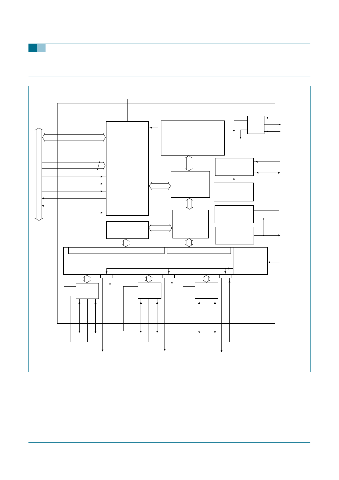
5. Block diagram
V
CC(I/O)
ISP1760
Embedded Hi-Speed USB host controller
37 to 39, 41 to 43,
45 to 47, 49, 51,
52, 54, 56 to 58,
60 to 62, 64 to 66,
68 to 70, 72 to 74,
76 to 78, 80
GENERIC PROCESSOR BUS
DATA[15:0]/DATA[31:0]
82, 84, 86, 87,
89, 91 to 93,
95 to 98,
100 to 103, 105
A[17:1]
106
CS_N
107
RD_N
108
WR_N
112
IRQ
114
DREQ
116
DACK
USB FULL-SPEED AND LOW SPEED DATA PATH
PORT ROUTING OR CONTROL LOGIC + HOST AND HUB PORT STATUS
RISC PROCESSOR
17
10, 40, 48, 59, 67,
75, 83, 94, 104, 115
INTERFACE:
MEMORY
MANAGEMENT
UNIT
+
INTERRUPT
CONTROL
+
SLAVE DMA
CONTROLLER
+
HARDWARE
CONFIGURATION
REGISTERS
TRANSACTION
TRANSLATOR
AND RAM
ISP1760
PTD AND PAYLOAD MEMORY:
16-bit
or
32-bit
INTERNAL MEMORY
UP TO 64 KBYTES
VIRTUAL SEGMENTATION
FOR MULTITASKING SUPPORT
MEMORY
ARBITER
AND FIFO
EHCI AND
OPERATIONAL
REGISTERS
PIE
USB HIGH-SPEED DATA PATH
30 MHz
60 MHz
GLOBAL CONTROL
AND POWER
MANAGEMENT
POWER-ON RESET
AND V
5 V-TO-1.8 V
REGULATOR
5 V-TO-3.3 V
REGULATOR
BAT
VOLTAGE
VOLTAGE
AND ANALOG
OVERCURRENT
DETECTION
ON
DIGITAL
PLL
122
119
110
5, 50,
85, 118
6, 7
11
12
13
9
2
XTAL1
XTAL2
CLKIN
RESET_N
SUSPEND/
WAKEUP_N
V
BAT_ON_N
V
REG(1V8)
V
CC(5V0)
V
REG(3V3)
REF5V
16
RREF1
GND
HI-SPEED
USB ATX1
15
DP1
20
GND
19
DM1
PSW1_N
18
21
127
OC1_N
23
RREF2
GND
22
DP2
HI-SPEED
USB ATX2
27
26
DM2
GND
PSW2_N
25
128
28
OC2_N
RREF3
30
GND
HI-SPEED
USB ATX3
29
34
DP3
GND
33
DM3
PSW3_N
32
35
OC3_N
1
4, 8, 14, 17, 24,
31, 36, 44, 53,
55, 63, 71, 79,
88, 90, 99, 109,
121, 123
004aaa435
GND
Fig 1. Block diagram.
9397 750 13257 © Koninklijke Philips Electronics N.V. 2004. All rights reserved.
Product data sheet Rev. 01 — 8 November 2004 4 of 105
Page 5
Philips Semiconductors
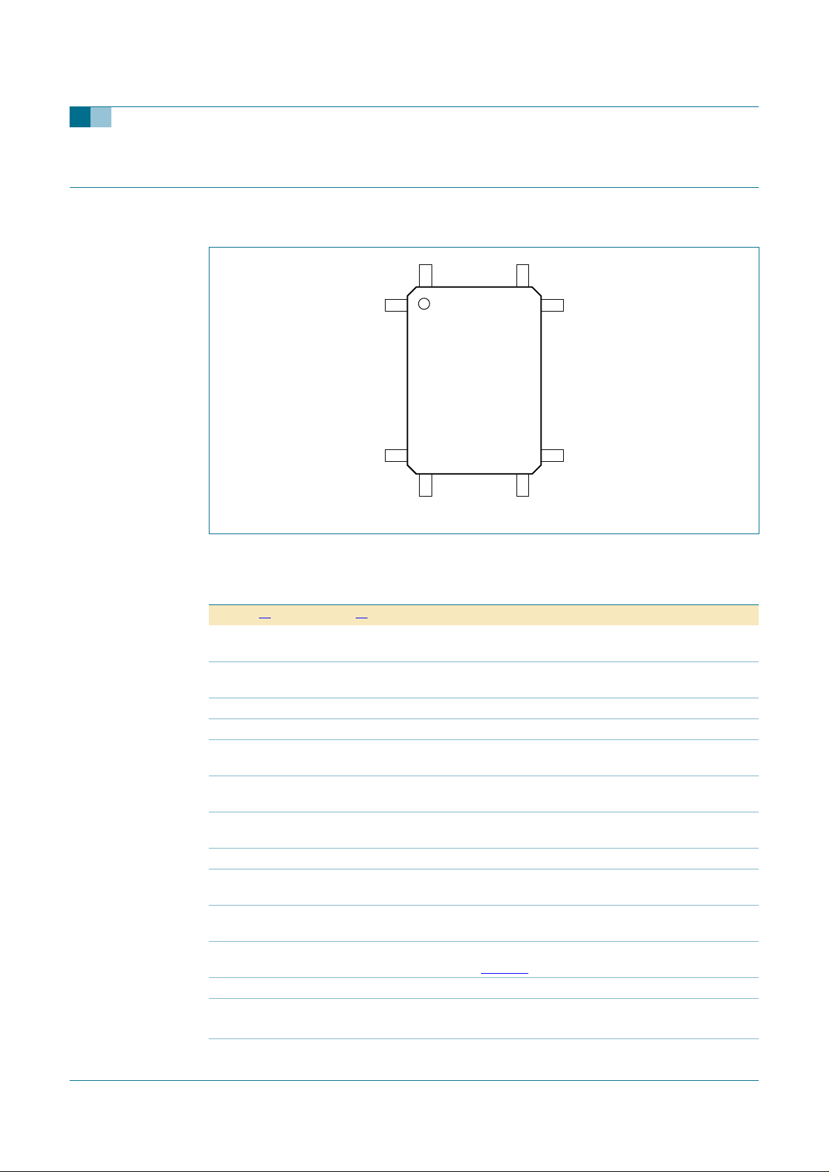
6. Pinning information
6.1 Pinning
ISP1760
Embedded Hi-Speed USB host controller
128
1
ISP1760BE
38
39
103
64
004aaa505
102
65
Fig 2. Pin configuration (LQFP128).
6.2 Pin description
Table 2: Pin description
Symbol
[1]
Pin Type
OC3_N 1 AI port 3 analog (5 V input) and digital overcurrent input; if not used,
REF5V 2 AI 5 V reference input for analog OC detector; connect a 100 nF
TEST 3 - connect to ground
GND 4 - analog ground
V
REG(1V8)
V
CC(5V0)
V
CC(5V0)
5 P core power output (1.8 V); internal 1.8 V for the digital core; used for
6 P input to internal regulators (3.0 V to 5.5 V); connect a 100 nF
7 P input to internal regulators (3.0 V to 5.5 V); connect a 100 nF
GND 8 - oscillator ground
V
REG(3V3)
V
CC(I/O)
9 P regulator output (3.3 V); for decoupling only; connect a 100 nF
10 P digital supply; 1.65 V to 3.6 V; connect a 100 nF decoupling
XTAL1 11 AI 12 MHz crystal connection input; connect to ground if an external
XTAL2 12 AO 12 MHz crystal connection output
CLKIN 13 I 12 MHz oscillator or clock input; connect to V
GND 14 - digital ground
[2]
Description
connect to V
through a 10 kΩ resistor
CC(I/O)
decoupling capacitor
decoupling; connect a 100 nF capacitor
decoupling capacitor
decoupling capacitor
capacitor and a 4.7 µFto10µF capacitor
capacitor
clock is used; see
Table 84
3.3 V tolerant
CC(I/O)
when not in use
9397 750 13257 © Koninklijke Philips Electronics N.V. 2004. All rights reserved.
Product data sheet Rev. 01 — 8 November 2004 5 of 105
Page 6

Philips Semiconductors
ISP1760
Embedded Hi-Speed USB host controller
Table 2: Pin description
CC(I/O)
[1]
Pin Type
40 P digital supply; 1.65 V to 3.6 V; connect a 100 nF decoupling
Symbol
GND 15 - RREF1 ground
RREF1 16 AI reference resistor connection; connect a 12 kΩ±1 % resistor
GND 17 - analog ground for port 1
DM1 18 AI/O downstream data minus port 1
GND 19 - analog ground
DP1 20 AI/O downstream data plus port 1
PSW1_N 21 OD power switch port 1, active LOW
GND 22 - RREF2 ground
RREF2 23 AI reference resistor connection; connect a 12 kΩ±1 % resistor
GND 24 - analog ground for port 2
DM2 25 AI/O downstream data minus port 2
GND 26 - analog ground
DP2 27 AI/O downstream data plus port 2
PSW2_N 28 OD power switch port 2, active LOW
GND 29 - RREF3 ground
RREF3 30 AI reference resistor connection; connect a 12 kΩ±1 % resistor
GND 31 - analog ground for port 3
DM3 32 AI/O downstream data minus port 3
GND 33 - analog ground
DP3 34 AI/O downstream data plus port 3
PSW3_N 35 OD power switch port 3, active LOW
GND 36 - digital ground
DATA0 37 I/O data bit 0 input and output
DATA1 38 I/O data bit 1 input and output
DATA2 39 I/O data bit 2 input and output
V
DATA3 41 I/O data bit 3 input and output
…continued
[2]
Description
between this pin and the RREF1 ground
output pad, push-pull open-drain, 8 mA output drive, 5 V tolerant
between this pin and the RREF2 ground
output pad, push-pull open-drain, 8 mA output drive, 5 V tolerant
between this pin and the RREF3 ground
output pad, push-pull open-drain, 8 mA output drive, 5 V tolerant
bidirectional pad, push-pull input, three-state output, 4 mA output
drive, 3.3 V tolerant
bidirectional pad, push-pull input, three-state output, 4 mA output
drive, 3.3 V tolerant
bidirectional pad, push-pull input, three-state output, 4 mA output
drive, 3.3 V tolerant
capacitor
bidirectional pad, push-pull input, three-state output, 4 mA output
drive, 3.3 V tolerant
9397 750 13257 © Koninklijke Philips Electronics N.V. 2004. All rights reserved.
Product data sheet Rev. 01 — 8 November 2004 6 of 105
Page 7

Philips Semiconductors
ISP1760
Embedded Hi-Speed USB host controller
Table 2: Pin description
Symbol
[1]
Pin Type
…continued
[2]
Description
DATA4 42 I/O data bit 4 input and output
bidirectional pad, push-pull input, three-state output, 4 mA output
drive, 3.3 V tolerant
DATA5 43 I/O data bit 5 input and output
bidirectional pad, push-pull input, three-state output, 4 mA output
drive, 3.3 V tolerant
GND 44 - digital ground
DATA6 45 I/O data bit 6 input and output
bidirectional pad, push-pull input, three-state output, 4 mA output
drive, 3.3 V tolerant
DATA7 46 I/O data bit 7 input and output
bidirectional pad, push-pull input, three-state output, 4 mA output
drive, 3.3 V tolerant
DATA8 47 I/O data bit 8 input and output
bidirectional pad, push-pull input, three-state output, 4 mA output
drive, 3.3 V tolerant
V
CC(I/O)
48 P digital supply; 1.65 V to 3.6 V; connect a 100 nF decoupling
capacitor
DATA9 49 I/O data bit 9 input and output
bidirectional pad, push-pull input, three-state output, 4 mA output
drive, 3.3 V tolerant
V
REG(1V8)
50 P core power output (1.8 V); internal 1.8 V forthe digital core; used for
decoupling; connect a 100 nF capacitor
DATA10 51 I/O data bit 10 input and output
bidirectional pad, push-pull input, three-state output, 4 mA output
drive, 3.3 V tolerant
DATA11 52 I/O data bit 11 input and output
bidirectional pad, push-pull input, three-state output, 4 mA output
drive, 3.3 V tolerant
GND 53 - core ground
DATA12 54 I/O data bit 12 input and output
bidirectional pad, push-pull input, three-state output, 4 mA output
drive, 3.3 V tolerant
GND 55 - digital ground
DATA13 56 I/O data bit 13 input and output
bidirectional pad, push-pull input, three-state output, 4 mA output
drive, 3.3 V tolerant
DATA14 57 I/O data bit 14 input and output
bidirectional pad, push-pull input, three-state output, 4 mA output
drive, 3.3 V tolerant
DATA15 58 I/O data bit 15 input and output
bidirectional pad, push-pull input, three-state output, 4 mA output
drive, 3.3 V tolerant
V
CC(I/O)
59 P digital supply; 1.65 V to 3.6 V; connect a 100 nF decoupling
capacitor
9397 750 13257 © Koninklijke Philips Electronics N.V. 2004. All rights reserved.
Product data sheet Rev. 01 — 8 November 2004 7 of 105
Page 8

Philips Semiconductors
ISP1760
Embedded Hi-Speed USB host controller
Table 2: Pin description
CC(I/O)
CC(I/O)
[1]
Pin Type
67 P digital supply; 1.65 V to 3.6 V; connect a 100 nF decoupling
75 P digital supply; 1.65 V to 3.6 V; connect a 100 nF decoupling
Symbol
DATA16 60 I/O data bit 16 input and output
DATA17 61 I/O data bit 17 input and output
DATA18 62 I/O data bit 18 input and output
GND 63 - digital ground
DATA19 64 I/O data bit 19 input and output
DATA20 65 I/O data bit 20 input and output
DATA21 66 I/O data bit 21 input and output
V
DATA22 68 I/O data bit 22 input and output
DATA23 69 I/O data bit 23 input and output
DATA24 70 I/O data bit 24 input and output
GND 71 - digital ground
DATA25 72 I/O data bit 25 input and output
DATA26 73 I/O data bit 26 input and output
DATA27 74 I/O data bit 27 input and output
V
DATA28 76 I/O data bit 28 input and output
…continued
[2]
Description
bidirectional pad, push-pull input, three-state output, 4 mA output
drive, 3.3 V tolerant
bidirectional pad, push-pull input, three-state output, 4 mA output
drive, 3.3 V tolerant
bidirectional pad, push-pull input, three-state output, 4 mA output
drive, 3.3 V tolerant
bidirectional pad, push-pull input, three-state output, 4 mA output
drive, 3.3 V tolerant
bidirectional pad, push-pull input, three-state output, 4 mA output
drive, 3.3 V tolerant
bidirectional pad, push-pull input, three-state output, 4 mA output
drive, 3.3 V tolerant
capacitor
bidirectional pad, push-pull input, three-state output, 4 mA output
drive, 3.3 V tolerant
bidirectional pad, push-pull input, three-state output, 4 mA output
drive, 3.3 V tolerant
bidirectional pad, push-pull input, three-state output, 4 mA output
drive, 3.3 V tolerant
bidirectional pad, push-pull input, three-state output, 4 mA output
drive, 3.3 V tolerant
bidirectional pad, push-pull input, three-state output, 4 mA output
drive, 3.3 V tolerant
bidirectional pad, push-pull input, three-state output, 4 mA output
drive, 3.3 V tolerant
capacitor
bidirectional pad, push-pull input, three-state output, 4 mA output
drive, 3.3 V tolerant
9397 750 13257 © Koninklijke Philips Electronics N.V. 2004. All rights reserved.
Product data sheet Rev. 01 — 8 November 2004 8 of 105
Page 9

Philips Semiconductors
ISP1760
Embedded Hi-Speed USB host controller
Table 2: Pin description
Symbol
[1]
Pin Type
…continued
[2]
Description
DATA29 77 I/O data bit 29 input and output
bidirectional pad, push-pull input, three-state output, 4 mA output
drive, 3.3 V tolerant
DATA30 78 I/O data bit 30 input and output
bidirectional pad, push-pull input, three-state output, 4 mA output
drive, 3.3 V tolerant
GND 79 - digital ground
DATA31 80 I/O data bit 31 input and output
bidirectional pad, push-pull input, three-state output, 4 mA output
drive, 3.3 V tolerant
TEST 81 - connect to ground
A1 82 I address pin 1
input, 3.3 V tolerant
V
CC(I/O)
83 P digital supply; 1.65 V to 3.6 V; connect a 100 nF decoupling
capacitor
A2 84 I address pin 2
input, 3.3 V tolerant
V
REG(1V8)
85 P core power output (1.8 V); internal 1.8 V forthe digital core; used for
decoupling; connect a 100 nF capacitor and a 4.7 µFto10µF
capacitor
A3 86 I address pin 3
input, 3.3 V tolerant
A4 87 I address pin 4
input, 3.3 V tolerant
GND 88 - core ground
A5 89 I address pin 5
input, 3.3 V tolerant
GND 90 - digital ground
A6 91 I address pin 6
input, 3.3 V tolerant
A7 92 I address pin 7
input, 3.3 V tolerant
A8 93 I address pin 8
input, 3.3 V tolerant
V
CC(I/O)
94 P digital supply; 1.65 V to 3.6 V; connect a 100 nF decoupling
capacitor
A9 95 I address pin 9
input, 3.3 V tolerant
A10 96 I address pin 10
input, 3.3 V tolerant
A11 97 I address pin 11
input, 3.3 V tolerant
A12 98 I address pin 12
input, 3.3 V tolerant
9397 750 13257 © Koninklijke Philips Electronics N.V. 2004. All rights reserved.
Product data sheet Rev. 01 — 8 November 2004 9 of 105
Page 10

Philips Semiconductors
ISP1760
Embedded Hi-Speed USB host controller
Table 2: Pin description
Symbol
[1]
Pin Type
…continued
[2]
Description
GND 99 - digital ground
A13 100 I address pin 13
input, 3.3 V tolerant
A14 101 I address pin 14
input, 3.3 V tolerant
A15 102 I address pin 15
input, 3.3 V tolerant
A16 103 I address pin 16
input, 3.3 V tolerant
V
CC(I/O)
104 P digital voltage; 1.65 V to 3.6 V; connect a 100 nF decoupling
capacitor
A17 105 I address pin 17
input, 3.3 V tolerant
CS_N 106 I chip select signal that indicates the area being accessed; active
LOW
input, 3.3 V tolerant
RD_N 107 I read enable; active LOW
input, 3.3 V tolerant
WR_N 108 I write enable; active LOW
input, 3.3 V tolerant
GND 109 - digital ground
V
BAT_ON_N
110 OD to indicate the presence of a minimum 3.3 V on pins 6 and 7
(open-drain); connect to V
through a 10 kΩ pull-up resistor
CC(I/O)
output pad, push-pull open-drain, 8 mA output drive, 5 V tolerant
n.c. 111 - not connected
IRQ 112 O Host Controller interrupt signal
output pad, 4 mA drive, 3.3 V tolerant
n.c. 113 - not connected
DREQ 114 O DMAC request for the Host Controller
output pad, 4 mA drive, 3.3 V tolerant
V
CC(I/O)
115 P digital voltage; 1.65 V to 3.6 V; connect a 100 nF decoupling
capacitor
DACK 116 I Host Controller DMA request acknowledgment; when not in use,
connect to V
through a 10 kΩ pull-up resistor
CC(I/O)
input, 3.3 V tolerant
TEST 117 - connect to ground
V
REG(1V8)
118 P core power output (1.8 V); internal 1.8 V forthe digital core; used for
decoupling; connect a 100 nF capacitor
SUSPEND/
WAKEUP_
N
119 I/OD Host Controller suspend and wake-up; three-state suspend output
(active LOW) and wake-up input circuits are connected together
• HIGH = output is three-state; ISP1760 is in suspend mode;
connect to V
through an external 10 kΩ pull-up resistor
CC(I/O)
• LOW = output is LOW; ISP1760 is not in suspend mode.
output pad, open-drain, 4 mA output drive, 3.3 V tolerant
9397 750 13257 © Koninklijke Philips Electronics N.V. 2004. All rights reserved.
Product data sheet Rev. 01 — 8 November 2004 10 of 105
Page 11

Philips Semiconductors
ISP1760
Embedded Hi-Speed USB host controller
Table 2: Pin description
Symbol
[1]
Pin Type
TEST 120 - pull up to V
…continued
[2]
Description
CC(I/O)
GND 121 - core ground
RESET_N 122 I external power-up reset; active LOW
input, 3.3 V tolerant
GND 123 - analog ground
TEST 124 - connect a 220 nF capacitor between this pin and pin 125
TEST 125 - connect a 220 nF capacitor between this pin and pin 124
TEST 126 - connect to 3.3 V
OC1_N 127 AI port 1 analog (5 V input) and digital overcurrent input; if not used,
connect to V
through a 10 kΩ resistor
CC(I/O)
OC2_N 128 AI port 2 analog (5 V input) and digital overcurrent input; if not used,
connect to V
[1] Symbol names ending with underscore N (for example, NAME_N) represent active LOW signals.
[2] I = input only; O = output only; I/O = digital input/output; OD = open-drain output; AI/O = analog
input/output; AI = analog input; P = power.
through a 10 kΩ resistor
CC(I/O)
9397 750 13257 © Koninklijke Philips Electronics N.V. 2004. All rights reserved.
Product data sheet Rev. 01 — 8 November 2004 11 of 105
Page 12

Philips Semiconductors
7. Functional description
7.1 ISP1760 internal architecture:Advanced Philips Slave Host Controller and hub
The EHCI block and the Hi-Speed USB hub block are the main components of the
Advanced Philips Slave Host Controller.
The EHCI is the latest generation design, with improved data bandwidth. The EHCI in the
ISP1760 is adapted from
Serial Bus Rev. 1.0
The internal Hi-Speed USB hub block replaces the companion Host Controller block used
in the original PCI Hi-Speed USB Host Controllers to handle the full-speed and low-speed
modes. The hardware architecture in the ISP1760 is simplified to help reduce cost and
development time, by eliminating the additional work involved in implementing the OHCI
software required to support the full-speed and low-speed modes.
Figure 3 shows the internal architecture of the ISP1760. The ISP1760 implements the
EHCI that has an internal port—the Root Hub port (not availableexternally)—on which the
internal hub is connected. The three external ports are always routed to the internal hub.
The internal hub is a Hi-Speed USB (USB 2.0) hub including the TT.
ISP1760
Embedded Hi-Speed USB host controller
Enhanced Host Controller Interface Specification for Universal
.
Remark: The root hub must be enabled and the internal hub must be enumerated.
Enumerate the internal hub as if it is externally connected. For details, refer to
Linux Programming Guide (AN10042)
At the Host Controller reset and initialization, the internal Root Hub port will be polled until
a new connection is detected, showing the connection of the internal hub.
The internal Hi-Speed USB hub is enumerated using a sequence similar to a standard
Hi-Speed USB hub enumeration sequence, and the polling on the Root Hub is stopped
because the internal Hi-Speed USB hub will never be disconnected. When enumerated,
the internal hub will report the three externally available ports.
.
ISP176x
9397 750 13257 © Koninklijke Philips Electronics N.V. 2004. All rights reserved.
Product data sheet Rev. 01 — 8 November 2004 12 of 105
Page 13
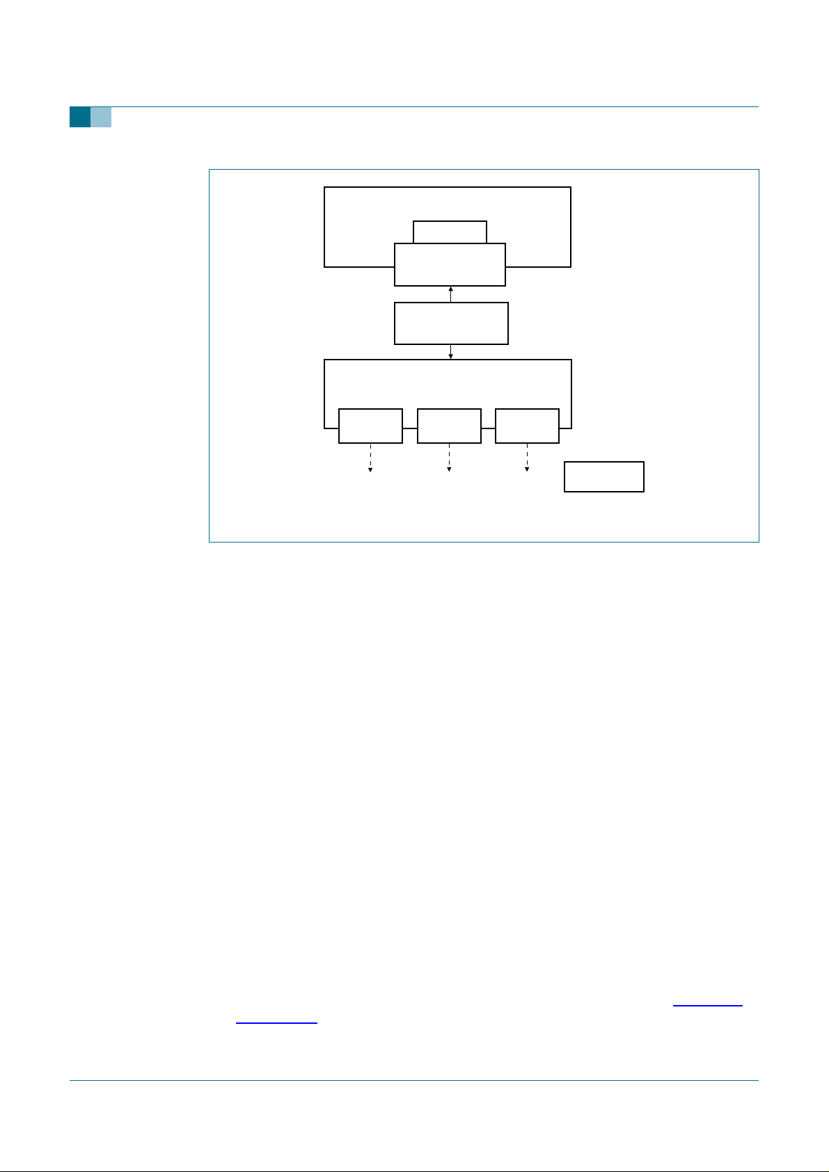
Philips Semiconductors
ISP1760
Embedded Hi-Speed USB host controller
EHCI
ROOT HUB
PORTSC1
ENUMERATION
AND POLLING USING
ACTUAL PTDs
INTERNAL HUB (TT)
PORT1
Fig 3. Internal hub.
PORT2
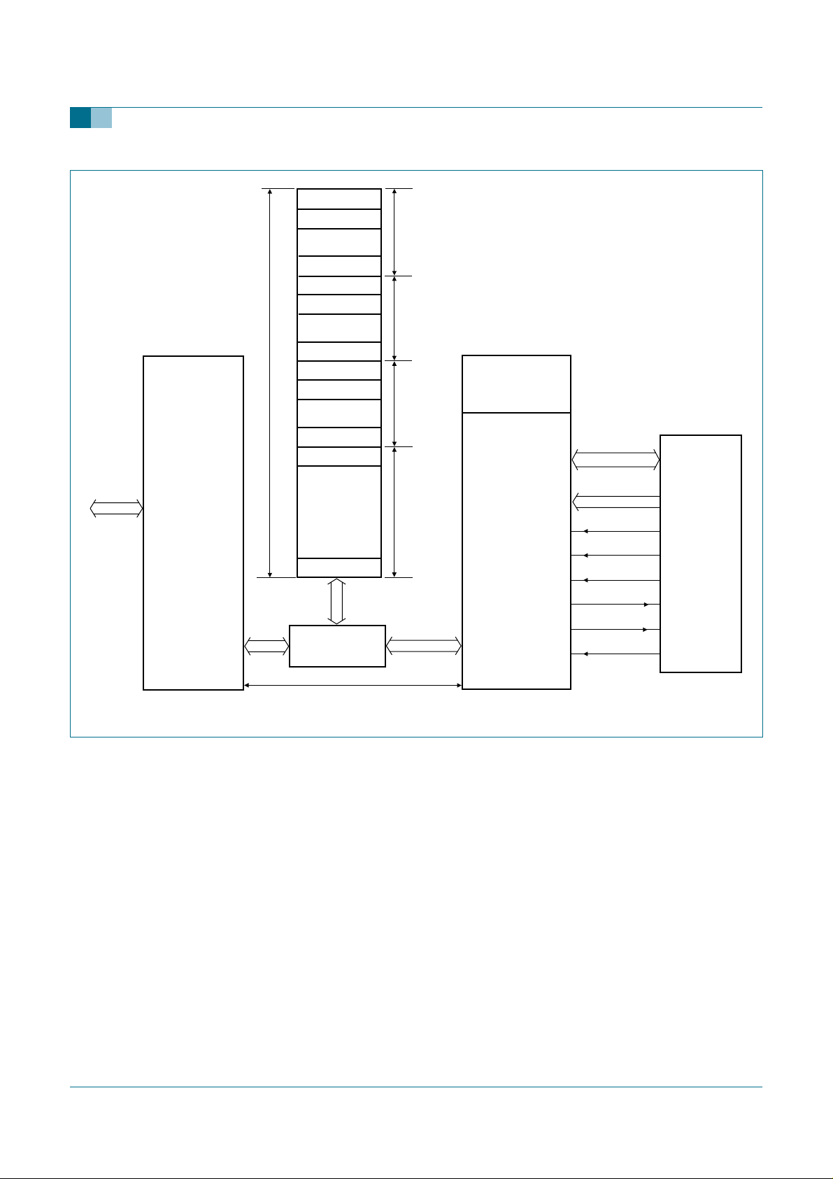
7.2 Host Controller buffer memory block
7.2.1 General considerations
The internal addressable Host Controller buffer memory is 63 kbytes. The 63-kbyte
effective memory size is the result of subtracting the size of registers (1 kbyte) from the
total addressable memory space defined in the ISP1760 (64 kbytes).This is the optimized
value for achieving the highest performance with a minimal cost.
The ISP1760 is a slave Host Controller. This means that it does not need access to the
local bus of the system to transfer data from the memory of the system to the ISP1760
internal memory, unlike the case of the original PCI Hi-Speed USB Host Controllers.
Therefore, correct data must be transferred to both the Philips Transfer Descriptor (PTD)
area and the payload area by Parallel I/O (PIO) (CPU access) or programmed DMA.
The ‘slave-host’ architecture ensures better compatibility with most of the processors
present in the market today because not all processors allow a ‘bus-master’ on the local
bus. It also allows better load balancing of the processor’s local bus because only the
internal bus arbiter of the processor controls the transfer of data dedicated to USB. This
preventsthe local bus from being busy when other more important transfersmay be in the
queue; and therefore achieving a ‘linear’ system data flow that has less impact on other
processes running at the same time.
PORT3
EXTERNAL
PORTS
004aaa513
The considerations mentioned are also the main reason for implementing the prefetching
technique, instead of using a READYsignal. The resulting architecture avoids ‘freezing’ of
the local bus (by asserting READY), enhancing the ISP1760 memory access time, and
avoiding introduction of programmed additional wait states. For details, see Section 7.3
and Section 8.3.8.
9397 750 13257 © Koninklijke Philips Electronics N.V. 2004. All rights reserved.
Product data sheet Rev. 01 — 8 November 2004 13 of 105
Page 14

Philips Semiconductors
The total amount of memory allocated to the payload determines the maximum transfer
size specified by a PTD—a larger internal memory size results in less CPU interruption for
transfer programming. This means less time spent in context switching, resulting in better
CPU usage.
A larger buffer also implies a larger amount of data can be transferred. The transfer,
however, can be done over a longer period of time, to maintain the overall system
performance. Each transfer of the USB data on the USB bus can span for up to a few
milliseconds before requiring further CPU intervention for data movement.
The internal architecture of the ISP1760 allows a flexible definition of the memory buffer
for optimization of the data transfer on the CPU extension bus and the USB. It is possible
to implement various data transfer schemes, depending on the number and type of USB
devices present (for example: push-pull—data can be written to half of the memory while
data in the other half is being accessed by the Host Controller and sent on the USB bus).
This is useful especially when a high-bandwidth ‘continuous or periodic’ data flow is
required.
Through an analysis of the hardware and software environment regarding the usual data
flow and performance requirements of most embedded systems, Philips has determined
the optimal size for the internal buffer as approximately 64 kbytes.
ISP1760
Embedded Hi-Speed USB host controller
7.2.2 Structure of the ISP1760 Host Controller memory
The 63-kbyte internal memory consists of the PTD area and the payload area.
Both the PTD and payload memory zones are divided into three dedicated areas for each
main type of USB transfer: isochronous (ISO), interrupt (INT) and Acknowledged Transfer
List (ATL). As shown in Table 3, the PTD areas for ISO, INT and ATL are grouped at the
beginning of the memory, occupying the address range 0400h to 0FFFh, following the
address space of the registers. The payload or data area occupies the next memory
address range 1000h to FFFFh, meaning that 60 kbytes of memory are allocated for the
payload data.
A maximum of 32 PTD areas and their allocated payload areas can be defined for each
type of transfer. The structure of a PTD is similar for every transfer type and consists of
eight Double Words (DWs) that must be correctly programmed for a correct USB data
transfer. The reserved bits of a PTD must be set to logic 0. A detailed description of the
PTD structure can be found in Section 9.
The transfer size specified by the PTD determines the contiguous USB data transfer that
can be performed without any CPU intervention. The respective payload memory area
must be equal to the transfer size defined. The maximum transfer size is flexible and can
be optimized, depending on the number and nature of USB devices or PTDs defined and
their respective MaxPacketSize.
The CPU will program the DMA to transfer the necessary data in the payload memory.
The next CPU intervention will be required only when the current transfer is completed
and DMA programming is necessary to transfer the next data payload. This is normally
signaled by the IRQ that is generated by the ISP1760 on completing the current PTD,
meaning all the data in the payload area was sent on the USB bus. The external IRQ
signal is asserted according to the settings in the IRQ Mask OR or IRQ Mask AND
registers, see Section 8.4.
9397 750 13257 © Koninklijke Philips Electronics N.V. 2004. All rights reserved.
Product data sheet Rev. 01 — 8 November 2004 14 of 105
Page 15

Philips Semiconductors
The RAM is structured in blocks of PTDs and payloads so that while the USB is executing
on an active transfer-based PTD, the processor can simultaneously fill up another block
area in the RAM. A PTD and its payload can then be updated on-the-fly without stopping
or delaying any other USB transaction or corrupting the RAM data.
Some of the design features are:
• The address range of the internal RAM buffer is from 0400h to FFFFh.
• The internal memory contains isochronous, interrupt and asynchronous PTDs, and
respective defined payloads.
• All accesses to the internal memory are double-word aligned.
• Internal memory address range calculation:
Memory address = (CPU address – 0400h) (shift right >> 3). Base address is 0400h.
Table 3: Memory address
Memory map CPU address Memory address
ISO 0400h to 07FFh 0000h to 007Fh
INT 0800h to 0BFFh 0080h to 00FFh
ATL 0C00h to 0FFFh 0100h to 017Fh
Payload 1000h to FFFFh 0180h to 1FFFh
ISP1760
Embedded Hi-Speed USB host controller
9397 750 13257 © Koninklijke Philips Electronics N.V. 2004. All rights reserved.
Product data sheet Rev. 01 — 8 November 2004 15 of 105
Page 16
Philips Semiconductors
ISP1760
Embedded Hi-Speed USB host controller
USB BUS
63 kbytes
USB HIGH-SPEED
HOST AND
TRANSACTION
TRANSLATOR
(FULL-SPEED
AND LOW-SPEED)
address
data (64 bits)
PTD1
PTD2
. .
PTD32
PTD1
PTD2
. .
PTD32
PTD1
PTD2
. .
PTD32
PAYLOAD
. . . . . . . .
PAYLOAD
ARBITER
240 MB/s
ISOCHRONOUS
INTERRUPT
ASYNC
PAYLOAD
REGISTERS
MEMORY MAPPED
INPUT/OUTPUT,
MEMORY
MANAGEMENT
UNIT,
SLAVE DMA
CONTROLLER
AND
INTERRUPT
CONTROL
D[15:0]/D[31:0]
A[17:1]
CS_N
RD_N
WR_N
IRQ
DREQ
DACK
MICRO-
PROCESSOR
control signals
004aaa436
Fig 4. Memory segmentation and access block diagram.
Both the CPU interface logic and the USB Host Controller require access to the internal
ISP1760 RAM at the same time. The internal arbiter controls these accesses to the
internal memory, organized internally on a 64-bit data bus width, allowing a maximum
bandwidth of 240 MB/s. This bandwidth avoids any bottleneck on accesses both from the
CPU interface and the internal USB Host Controller.
7.3 Accessing the ISP1760 Host Controller memory: PIO and DMA
The CPU interface of the ISP1760 can be configured for a 16-bit or 32-bit data bus width.
When the ISP1760 is configured for a 16-bit data bus width, the upper unused 16 data
lines must be pulled up to V
together to a single 10 kΩ pull-up resistor. The 16-bit or 32-bit data bus width
configuration is done by programming bit 8 of the HW Mode Control register. This will
determine the register and memory access types in both PIO and DMA modes to all
internal blocks: Host Controller, Peripheral Controller and OTG Controller. All accesses
must be word-aligned for 16-bit mode and double-word aligned for 32-bit mode, where
one word = 16 bits. When accessing the Host Controller registers in 16-bit mode, the
9397 750 13257 © Koninklijke Philips Electronics N.V. 2004. All rights reserved.
Product data sheet Rev. 01 — 8 November 2004 16 of 105
. This can be achieved by connecting DATA[31:16] lines
CC(I/O)
Page 17

Philips Semiconductors
register access must alwaysbe completed using two subsequent accesses. In the case of
a DMA transfer, the 16-bit or 32-bit data bus width configuration will determine the number
of bursts that will complete a certain transfer length.
In PIO mode, CS_N, WR_N and RD_N are used to access registers and memory. In DMA
mode, the data validation is performed by DACK—instead of CS_N—together with the
WR_N and RD_N signals. The DREQ signal will always be asserted as soon as the
ISP1760 DMA is enabled, as described in the following section.
7.3.1 PIO mode access—memory read cycle
The following method has been implemented to reduce the read access timing in the case
of a memory read:
• The Memory register contains the starting address and the bank selection to read
from the memory. Before every new read cycle of the same or different banks, an
appropriate value is written to this register.
• Once a value is written to this register, the address is stored in the FIFO of that bank
and is then used to prefetch data for the memory read of that bank.
For every subsequent read operation executed at a contiguous address, the address
pointer corresponding to that bank is automatically incremented to prefetch the next
data to be sent to the CPU.
Memory read accesses for multiple banks can be interleaved. In this case, the FIFO
block handles the MUXing of appropriate data to the CPU.
• The address written to the Memory register is incremented and used to successively
prefetch data from the memory irrespective of the value on the address bus for each
bank, until a new value for a bank is written to the Memory register.
For example, consider the following sequence of operations:
– Write the starting (read) address 4000h and bank1 = 01 to the Memory register.
– Write the starting (read) address 4100h and bank2 = 10 to the Memory register.
ISP1760
Embedded Hi-Speed USB host controller
When RD_N is asserted for three cycles with A[17:16] = 01, the returned data
corresponds to addresses 4000h, 4004h and 4008h.
Remark: Once 4000h is written to the Memory register for bank1, the bank select
value determines the successive incremental addresses used to fetch the data.
That is, the fetching of data is independent of the address on A[15:0] lines.
When RD_N is asserted for four cycles with A[17:16] = 10, the returned data
corresponds to addresses 4100h, 4104h, 4108h and 410Ch.
Consequently, the RD_N assertion with A[17:16] = 01 will return data from 400Ch
because the bank1 read stopped there in the previous cycle. Also, RD_N
assertions with A[17:16] = 010 will now return data from 4110h because the bank2
read stopped there in the previous cycle.
7.3.2 PIO mode access—memory write cycle
The PIO memory write access is similar to a normal memory access. It is not necessary
to set the prefetching address before a write cycle to the memory.
The ISP1760 internal write address will not be automatically incremented during
consecutive write accesses, unlike in a series of ISP1760 memory read cycles. The
memory write address must be incremented before every access.
9397 750 13257 © Koninklijke Philips Electronics N.V. 2004. All rights reserved.
Product data sheet Rev. 01 — 8 November 2004 17 of 105
Page 18

Philips Semiconductors
7.3.3 PIO mode access—register read cycle
The PIO register read access is similar to a general register access. It is not necessary to
set a prefetching address before a register read.
The ISP1760 register read address will not be automatically incremented during
consecutive read accesses, unlike in a series of ISP1760 memory read cycles. The
ISP1760 register read address must be correctly specified before every access.
7.3.4 PIO mode access—register write cycle
The PIO register write access is similar to a general register access. It is not necessary to
set a prefetching address before a register write.
The ISP1760 register write address will not be automatically incremented during
consecutive write accesses, unlike in a series of ISP1760 memory read cycles. The
ISP1760 register write address must be correctly specified before every access.
7.3.5 DMA—read and write operations
The internal ISP1760 Host Controller DMA is a slave DMA. The host system processor or
DMA must ensure the data transfer to or from the ISP1760 memory.
ISP1760
Embedded Hi-Speed USB host controller
The ISP1760 DMA supports a DMA burst length of 1, 4, 8 and 16 cycles forboth the 16-bit
and 32-bit data bus width. DREQ will be asserted at the beginning of the first burst of a
DMA transfer and will be deasserted on the last cycle (RD_N or WR_N active pulse) of
that burst. It will be reasserted shortly after the DACK deassertion, as long as the DMA
transfer counter was not reached. DREQ will be deasserted on the last cycle when the
DMA transfer counter is reached and will not reasserted until the DMA reprogramming is
performed. Both the DREQ and DACK signals are programmable as active LOW or active
HIGH, according to the system requirements.
The DMA start address must be initialized in the respective register, and the subsequent
transfers will automatically increment the internal ISP1760 memory address. A register or
memory access or access to other system memory can occur in between DMA bursts,
whenever the bus is released because DACK is deasserted, without affecting the DMA
transfer counter or the current address.
Any memory area can be accessed by the system’sDMA at any starting address because
there are no predefined memory blocks. The DMA transfer must start on a word or Double
Word address, depending on whether the data bus width is set to 16 bit or 32 bit. DMA is
the most efficient method to initialize the payload area, to reduce the CPU usage and
overall system loading.
The ISP1760 does not implement EOT to signal the end of a DMA transfer. If
programmed, an interrupt may be generated by the ISP1760 at the end of the DMA
transfer.
The slave DMA of the ISP1760 will issue a DREQ to the DMA controller of the system to
indicate that it is programmed for transfer and data is ready. The system DMA controller
may also start a transfer without the need of the DREQ, if the ISP1760 memory is
available for the data transfer and the ISP1760 DMA programming is completed.
9397 750 13257 © Koninklijke Philips Electronics N.V. 2004. All rights reserved.
Product data sheet Rev. 01 — 8 November 2004 18 of 105
Page 19

Philips Semiconductors
It is also possible that the system’s DMA will perform a memory-to-memory type of
transfer between the system memory and the ISP1760 memory. The ISP1760 will be
accessed in the PIO mode. Consequently, memory read operations must be preceded by
initializing the Memory register (address 033Ch), as described in Section 7.3.1. No IRQ
will be generated by the ISP1760 on completing the DMA transfer but an internal
processor interrupt may be generated to signal that the DMA transfer is completed. This is
mainly useful in implementing the double-buffering scheme for data transfer to optimize
the USB bandwidth.
The ISP1760 DMA programming involves:
• Set the active levels of signals DREQ and DACK in the HW Mode Control register.
• The DMA Start Address register contains the first memory address at which the data
transfer will start. It must be word-aligned in the 16-bit data bus mode and double
word aligned in the 32-bit data bus mode.
• The programming of the DMA Configuration register specifies:
– The type of transfer that will be performed: read or write
– The burstsize—expressed in bytes—is specified, regardless of the data bus width.
– The transferlength—expressed in number of bytes—defines the number of bursts.
– Enable ENABLE_DMA (bit 1) of the DMA Configuration register to determine the
ISP1760
Embedded Hi-Speed USB host controller
For the same burst size, a double number of cycles will be generated in the 16-bit
mode data bus width as compared to the 32-bit mode.
The DREQ will be deasserted and asserted to generate the next burst, as long as
there are bytes to be transferred. At the end of a transfer, the DREQ will be
deasserted and an IRQ can be generated if DMAEOTINT (bit 3 in the Interrupt
register) is set. The maximum DMA transfersize is equal to the maximum memory
size. The transfer size can be an odd or even number of bytes, as required. If the
transfer size is an odd number of bytes, the number of bytes transferred by the
system’s DMA is equal to the next multiple of two for the 16-bit data bus width or
four for the 32-bit data bus width. For a write operation, however, only the specified
odd number of bytes in the ISP1760 memory will be affected.
assertion of DREQ immediately after setting the bit.
After programming the preceding parameters, the system’sDMA maybe enabled (waiting
for the DREQ to start the transfer or immediate transfer may be started).
The programming of the system’s DMA must match the ISP1760 DMA parameters
programmed above. Only one DMA transfer may take place at a time. A PIO mode data
transfer may occur simultaneously with a DMA data transfer, in the same or a different
memory area.
7.4 Interrupts
The ISP1760 will assert an IRQ according to the source or event in the Interrupt register.
The main steps to enable the IRQ assertion are:
1. Set GLOBAL_INTR_EN (bit 0) in the HW Mode Control register.
2. Define the IRQ active as levelor edge in INTR_LEVEL (bit 1) of the HW Mode Control
register.
9397 750 13257 © Koninklijke Philips Electronics N.V. 2004. All rights reserved.
Product data sheet Rev. 01 — 8 November 2004 19 of 105
Page 20

Philips Semiconductors
3. Define the IRQ polarity as active LOW or active HIGH in INTR_POL (bit 2) of the HW
Mode Control register. These settings must match the IRQ settings of the host
processor.
By default, interrupt is level-triggered and active LOW.
4. Program the individual interrupt enable bits in the Interrupt Enable register. The
software will need to clear the interrupt status bits in the Interrupt register before
enabling individual interrupt enable bits.
Additional IRQ characteristics can be adjusted in the Edge Interrupt Count register, as
necessary, applicableonly when IRQ is set to be edge-active (a pulse of a defined width is
generated every time IRQ is active).
Bits 15 to 0 of the Edge Interrupt Count register define the IRQ pulse width. The maximum
pulse width that can be programmed is FFFFh, corresponding to a 1 ms pulse width. This
setting is necessary for certain processors that may require a different minimum IRQ
pulse width than the default value. The default IRQ pulse width set at power on is
approximately 500 ns.
Bits 31 to 24 of the Edge Interrupt Count register define the minimum interval between
two interrupts to avoid frequent interrupts to the CPU. The default value of 00h attributed
to these bits determines the normal IRQ generation, without any delay. When a delay is
programmed and the IRQ becomes active after the respective delay, several IRQ events
may have already occurred.
ISP1760
Embedded Hi-Speed USB host controller
All the interrupt events are represented by the respective bits allocated in the Interrupt
register. There is no mechanism to show the order or the moment of occurrence of an
interrupt.
The asserted bits in the Interrupt register can be cleared by writing back the same valueto
the Interrupt register. This means that writing logic 1 to each of the set bits will reset the
corresponding bits to the initial inactive state.
The IRQ generation rules that apply according to the preceding settings are:
• If an event of interrupt occurs but the respective bit in the Interrupt Enable register is
not set, then the respective Interrupt register bit is set but the interrupt signal is not
asserted.
An interrupt will be generated when interrupt is enabled and the respective bit in the
Interrupt Enable register is set.
• For a level trigger, an interrupt signal remains asserted until the processor clears the
Interrupt register by writing logic 1 to clear the Interrupt register bits that are set.
• If an interrupt is made edge-sensitive and is asserted, writing to clear the Interrupt
register will not have any effect because the interrupt will be asserted for a prescribed
amount of clock cycles.
• The clock stopping mechanism does not affect the generation of an interrupt. This is
useful during the suspend and resume cycles, when an interrupt is generated to
signal a wake-up event.
The IRQ generation can also be conditioned by programming the IRQ Mask OR and
IRQ Mask AND registers. Setting some of the bits in these registers to logic 1 will
determine the IRQ generation only when the respective AND or OR conditions of
completing the respective PTDs is met.
9397 750 13257 © Koninklijke Philips Electronics N.V. 2004. All rights reserved.
Product data sheet Rev. 01 — 8 November 2004 20 of 105
Page 21

Philips Semiconductors
With the help of the IRQ Mask AND and IRQ Mask OR registers for each type of
transfer—ISO, INT and bulk—software can determine which PTDs get priority and an
interrupt will be generated when the AND or OR conditions are met. The PTDs that are
set will wait until the respective bits of the remaining PTDs are set and then all PTDs
generate an interrupt request to the CPU together.
The registers definition shows that the AND or OR conditions are applicable to the same
category of PTDs—ISO, INT, ATL.
When an IRQ is generated, the PTD Done Map registers and the respective V bits will
show which PTDs were completed.
The rules that apply to the IRQ Mask AND or IRQ Mask OR settings are:
• TheOR mask has a higher priority over the AND mask. An IRQ is generated if bit n of
the done map is set and the corresponding bit n of the OR Mask register is set.
• If the OR mask for any done bit is not set, then the AND mask comes into picture. An
IRQ is generated if all the corresponding done bits of the AND Mask register are set.
For example: If bits 2, 4 and 10 are set in the AND Mask register, an IRQ is generated
only if bits 2, 4, 10 of the done map are set.
• If using the IRQ interval setting for the bulk PTD, an interrupt will only occur at the
regular time interval as programmed in the ATL Done Timeout register. Even if an
interrupt event occurs before the timeout of the register, no IRQ will be generated until
the time is up.
ISP1760
Embedded Hi-Speed USB host controller
For an example on using the IRQ Mask AND or IRQ Mask OR registers without the ATL
Done Timeout register, see Table 4.
The AND function: Activate the IRQ only if PTDs 1, 2 and 4 are done.
The OR function: If any of the PTDs 7, 8 or 9 are done, an IRQ for each of the PTD will be
raised.
Table 4: Using the IRQ Mask AND or IRQ Mask OR registers
PTD AND register OR register Time PTD done IRQ
11 0 1ms1 21 0 - 1 30 0 - - 4 1 0 3 ms 1 active because of AND
50 0 - - 60 0 - - 7 0 1 5 ms 1 active because of OR
8 0 1 6 ms 1 active because of OR
9 0 1 7 ms 1 active because of OR
7.5 Phase-Locked Loop (PLL) clock multiplier
The internal PLL requires a 12 MHz input, which can be a 12 MHz crystal or a 12 MHz
clock already existing in the system with a precision better than 50 ppm. This allows the
use of a low-cost 12 MHz crystal that also minimizes Electro-Magnetic Interference (EMI).
When an external crystal is used, make sure the CLKIN pin is connected to V
CC(I/O)
.
9397 750 13257 © Koninklijke Philips Electronics N.V. 2004. All rights reserved.
Product data sheet Rev. 01 — 8 November 2004 21 of 105
Page 22

Philips Semiconductors
The PLL block generates all the main internal clocks required for normal functionality of
various blocks: 30 MHz, 48 MHz and 60 MHz.
No external components are required for the PLL operation.
7.6 Power management
The ISP1760 implements a flexible power management scheme, allowing various power
saving stages.
The usual powering scheme implies programming EHCI registers and the internal
Hi-Speed USB (USB 2.0) hub in the same way it is done in the case of a PCI Hi-Speed
USB Host Controller with a Hi-Speed USB hub attached.
When the ISP1760 is in suspend mode, the main internal clocks will be stopped to ensure
minimum power consumption. An internal LazyClock of 100 kHz ± 40 % will continue
running. This allows initiating a resume on one of the following events:
• External USB device connect or disconnect
• Assertion of the CS_N signal because of any access to the ISP1760
• Driving the SUSPEND/WAKEUP_N pin to a LOW level.
ISP1760
Embedded Hi-Speed USB host controller
The SUSPEND/WAKEUP_N pin is a bidirectional pin. This pin should be connected to
one of the GPIO pins of a processor.
The awake state can be verified by reading the LOW level of this pin. If the level is HIGH,
it means that the ISP1760 is in the suspend state.
The SUSPEND/WAKEUP_N pin requires a pull-up because in the ISP1760 suspended
state the pin becomes three-state and can be pulled down, driving it externally by
switching the processor’s GPIO line to the output mode to generate the ISP1760 wake-up.
The SUSPEND/WAKEUP_N pin is a three-state output. It is also an input to the internal
wake-up logic.
When in suspend mode, the ISP1760 internal wake-up circuitry will sense the status of
the SUSPEND/WAKEUP_N pin:
• If it remains pulled-up, no wake-up is generated because a HIGH is sensed by the
internal wake-up circuit.
• If the pin is externally pulled LOW (for example, by the GPIO line or just as a test by
jumper), the input to the wake-up circuitry becomes LOW and the wake-up is
internally initiated.
The resume state has a clock-off count timer defined by bits 31 to 16 of the Power Down
Control register. The default value of this timer is 10 ms, meaning that the resume state
will be maintained for 10 ms. If during this time, the RUN/STOP bit in the USBCMD
register is set to logic 1, the Host Controller will go into a permanent resume—the normal
functional state. If the RUN/STOP bit is not set during the time determined bythe clock-off
count, the ISP1760 will switch back to suspend mode after the specified time. The
maximum delay that can be programmed in the clock-off count field is approximately
500 ms.
9397 750 13257 © Koninklijke Philips Electronics N.V. 2004. All rights reserved.
Product data sheet Rev. 01 — 8 November 2004 22 of 105
Page 23

Philips Semiconductors
Additionally, the Power Down Control register allows the ISP1760 internal blocks to be
disabled for lower power consumption as defined in Table 5.
The lowest suspend current that can be achieved is approximately 100 µA at room
temperature. The suspend current will increase with the increase in temperature, with
approximately 300 µA at 40 °C and up to a typical 1 mA at 85 °C. The system is not in
suspend mode when its temperature increases above 40 °C. Therefore, even a 1 mA
current consumption by the ISP1760 (in suspend mode) can be considered negligible. In
normal environmental conditions, when the system is in suspend mode, the maximum
ISP1760 temperature will be approximately 40 °C (determined by the ambient
temperature) so the ISP1760 maximum suspend current will be below 300 µA. An
alternative solution to achieve a very low suspend current is to completely switch off the
V
CC(5V0)
pins of the processor. This is possible because the ISP1760 can be used in the hybrid
mode, which allows only the V
The time from wake-up to suspend will be approximately 100 ms when the ISP1760
power is always on.
It is necessary to wait for the CLK_RDY interrupt assertion before programming the
ISP1760 because internal clocks are stopped during deep-sleep suspend and restarted
after the first wake-up event. The occurrence of the CLK_RDY interrupt means that the
internal clocks are running and the normal functionality is achieved.
ISP1760
Embedded Hi-Speed USB host controller
power input by using an external PMOS transistor, controlled by one of the GPIO
powered on to avoid loading of the system bus.
CC(I/O)
It is estimated that the CLK_RDY interrupt will be generated less than 100 µs after the
wake-up event, if the power to the ISP1760 was on during suspend.
If the ISP1760 is used in the hybrid mode and V
CC(5V0)
is off during suspend, a 2 ms reset
pulse is required when the power is switched back to on, before starting to program the
resume state. This will ensure that the internal clocks are running and all logics reach a
stable initial state.
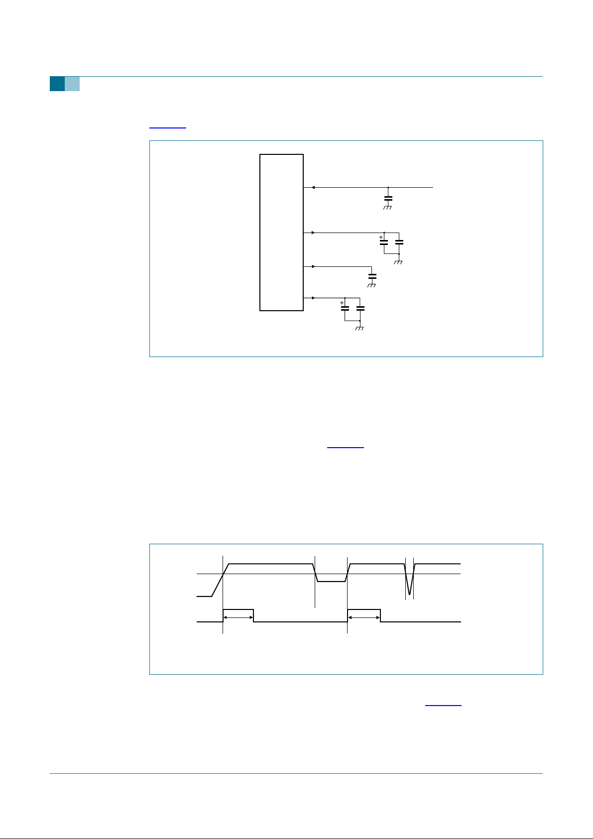
7.7 Overcurrent detection
The ISP1760 can implement a digital or analog overcurrent detection scheme. Bit 15 of
the HW Mode Control register can be programmed to select the analog or digital
overcurrent detection. An analog overcurrent detection circuit is integrated on-chip. The
main features of this circuit are self reporting, automatic resetting, low-trip time and low
cost. This circuit offers an easy solution at no extra hardware cost on the board. The port
power will be automatically disabled by the ISP1760 on an overcurrent event occurrence,
by deasserting the PSWn_N signal without any software intervention.
When using the integrated analog overcurrent detection, the range of the overcurrent
detection voltage for the ISP1760 is 45 mV to 100 mV. Calculation of the external
components should be based on the 45 mV value, with the actual overcurrent detection
threshold usually positioned in the middle of the interval.
Foran overcurrentlimit of 500 mA per port, a PMOS with R
is required. If a PMOS with a lower R
is used, analog overcurrent detection can be
DSON
adjusted using a series resistor; see Figure 5.
of approximately 100 mΩ
DSON
∆V
9397 750 13257 © Koninklijke Philips Electronics N.V. 2004. All rights reserved.
Product data sheet Rev. 01 — 8 November 2004 23 of 105
PMOS
∆V
= ∆V
= voltage drop on PMOS
PMOS
TRIP
= ∆V
TRIP(intrinsic)
− (I
OC(nom)
× Rtd), where:
Page 24
Philips Semiconductors
ISP1760
Embedded Hi-Speed USB host controller
I
OC(nom)
=1µA.
5 V
REF5V
PSWn_N
I
OC
(1)
R
td
OCn_N
ISP1760
004aaa662
(1) Rtd is optional.
Fig 5. Adjusting analog overcurrent detection limit (optional).
The digital overcurrent scheme requires using an external power switch with integrated
overcurrent detection, such as: LM3526, MIC2526 (2 ports) or LM3544 (4 ports). These
devices are controlled by PSWn_N signals corresponding to each port. In the case of
overcurrent occurrence, these devices will assert OCn_N signals. On OCn_N assertion,
the ISP1760 cuts off the port power by deasserting PSWn_N. The external integrated
power switch will also automatically cut-off the port power in the case of an overcurrent
event, by implementing thermal shutdown. An internal delay filter of 1 ms to 3 ms will
prevent false overcurrent reporting because of in-rush currents when plugging a USB
device.
7.8 Power supply
Figure 6 shows the ISP1760 power supply connection.
ISP1760
V
CC(5V0)
6, 7
10, 40, 48,
59, 67, 75,
83, 94,
104, 115
5, 50, 118
004aaa533
V
CC(I/O)
V
REG(1V8)
85
10 µF
V
REG(1V8)
V
REG(3V3)
9
10 µF
100 nF
Fig 6. ISP1760 power supply connection.
9397 750 13257 © Koninklijke Philips Electronics N.V. 2004. All rights reserved.
Product data sheet Rev. 01 — 8 November 2004 24 of 105
3.3 V to 5 V
100 nF
1.65 V to 3.6 V
100 nF
100 nF
100 nF
Page 25
Philips Semiconductors
Figure 7 shows the most commonly used power supply connection.
Fig 7. Most commonly used power supply connection.
ISP1760
6, 7, 10,
40, 48, 59,
67, 75, 83,
94, 104, 115
5, 50, 118
004aaa534
ISP1760
Embedded Hi-Speed USB host controller
V
, V
CC(5V0)
V
REG(1V8)
85
V
REG(1V8)
V
REG(3V3)
9
10 µF
CC(I/O
)
10 µF
100 nF
3.3 V
100 nF
100 nF
100 nF
7.9 Power-on reset (POR)
When V
(t
) will be typically 800 ns. The pulse is started when V
PORP
(1.2 V).
To give a better view of the functionality, Figure 8 shows a possible curve of V
dips at t2–t3 and t4–t5. If the dip at t4–t5 is too short (that is, < 11 µs), the internal POR
pulse will not react and will remain LOW. The internal POR starts with a 1 at t0. At t1, the
detector will see the passing of the trip level and a delay element will add another t
before it drops to 0.
The internal POR pulse will be generated whenever V
than 11 µs.
Fig 8. Internal power-on reset timing.
is directly connected to the RESET_N pin, the internal POR pulse width
CC(5V0)
rises above V
CC(5V0)
drops below V
CC(5V0)
V
V
t0 t1
t
PORP
t2
t3
t
PORP
t4
t5
004aaa584
PORP
(1) PORP = power-on reset pulse.
CC(5V0)
TRIP
CC(5V0)
TRIP
(1)
TRIP
with
PORP
for more
The RESET_N pin can be either connected to V
(using the internal POR circuit) or
CC(I/O)
externally controlled (by the microcontroller, ASIC, and so on). Figure 9 shows the
availability of the clock with respect to the external POR.
9397 750 13257 © Koninklijke Philips Electronics N.V. 2004. All rights reserved.
Product data sheet Rev. 01 — 8 November 2004 25 of 105
Page 26

Philips Semiconductors
Fig 9. Clock with respect to the external power-on reset.
ISP1760
Embedded Hi-Speed USB host controller
RESET_N
EXTERNAL CLOCK
004aaa583
A
Stable external clock is available at A.
9397 750 13257 © Koninklijke Philips Electronics N.V. 2004. All rights reserved.
Product data sheet Rev. 01 — 8 November 2004 26 of 105
Page 27

Philips Semiconductors
8. Registers
Table 5 shows the bit description of the registers.
• All registers range from 0000h to 03FFh. These registers can be read or written as
double word, that is 32-bit data. In the case of a 16-bit data bus width, two subsequent
accesses are necessary to complete the register read or write cycle.
• Operational registers range from 0000h to 01FFh. Configuration registers range from
0300h to 03FFh.
Table 5: Register overview
Address Register Reset value References
EHCI capability registers
0000h CAPLENGTH 20h
0002h HCIVERSION 0100h
0004h HCSPARAMS 0000 0011h
0008h HCCPARAMS 0000 0086h
EHCI operational registers
0020h USBCMD 0008 0000h
0024h USBSTS 0000 1000h
0028h USBINTR 0000 0000h
002Ch FRINDEX 0000 0000h
0030h CTRLDSSEGMENT 0000 0000h
0060h CONFIGFLAG 0000 0000h
0064h PORTSC1 0000 2000h
0130h ISO PTD Done Map 0000 0000h
0134h ISO PTD Skip Map FFFF FFFFh
0138h ISO PTD Last PTD 0000 0000h
0140h INT PTD Done Map 0000 0000h
0144h INT PTD Skip Map FFFF FFFFh
0148h INT PTD Last PTD 0000 0000h
0150h ATL PTD Done Map 0000 0000h
0154h ATL PTD Skip Map FFFF FFFFh
0158h ATL PTD Last PTD 0000 0000h
0200h–02FFh reserved - -
Configuration registers
0300h HW Mode Control 0000 0000h
0304h Chip ID 0001 1761h
0308h Scratch 0000 0000h
030Ch SW Reset 0000 0000h
0330h DMA Configuration 0000 0000h
0334h Buffer Status 0000 0000h
0338h ATL Done Timeout 0000 0000h
033Ch Memory 0000 0000h
ISP1760
Embedded Hi-Speed USB host controller
Section 8.1.1 on page 28
Section 8.1.2 on page 28
Section 8.1.3 on page 28
Section 8.1.4 on page 29
Section 8.2.1 on page 30
Section 8.2.2 on page 31
Section 8.2.3 on page 32
Section 8.2.4 on page 33
Section 8.2.5 on page 34
Section 8.2.6 on page 34
Section 8.2.7 on page 35
Section 8.2.8 on page 36
Section 8.2.9 on page 37
Section 8.2.10 on page 37
Section 8.2.11 on page 37
Section 8.2.12 on page 38
Section 8.2.13 on page 38
Section 8.2.14 on page 38
Section 8.2.15 on page 38
Section 8.2.16 on page 39
Section 8.3.1 on page 39
Section 8.3.2 on page 41
Section 8.3.3 on page 41
Section 8.3.4 on page 41
Section 8.3.5 on page 42
Section 8.3.6 on page 43
Section 8.3.7 on page 44
Section 8.3.8 on page 44
9397 750 13257 © Koninklijke Philips Electronics N.V. 2004. All rights reserved.
Product data sheet Rev. 01 — 8 November 2004 27 of 105
Page 28

Philips Semiconductors
ISP1760
Embedded Hi-Speed USB host controller
Table 5: Register overview
Address Register Reset value References
0340h Edge Interrupt Count 0000 000Fh Section 8.3.9 on page 45
0344h DMA Start Address 0000 0000h
0354h Power Down Control 03E8 1BA0h
0374h Port 1 Control 0086 0086h
Interrupt registers
0310h Interrupt 0000 0000h
0314h Interrupt Enable 0000 0000h
0318h ISO IRQ Mask OR 0000 0000h
031Ch INT IRQ Mask OR 0000 0000h
0320h ATL IRQ Mask OR 0000 0000h
0324h ISO IRQ Mask AND 0000 0000h
0328h INT IRQ Mask AND 0000 0000h
032Ch ATL IRQ Mask AND 0000 0000h
…continued
8.1 EHCI capability registers
8.1.1 CAPLENGTH register (R: 0000h)
The bit description of the Capability Length (CAPLENGTH) register is given in Table 6.
Section 8.3.10 on page 46
Section 8.3.11 on page 46
Section 8.3.12 on page 48
Section 8.4.1 on page 50
Section 8.4.2 on page 51
Section 8.4.3 on page 53
Section 8.4.4 on page 53
Section 8.4.5 on page 53
Section 8.4.6 on page 54
Section 8.4.7 on page 54
Section 8.4.8 on page 54
Table 6: CAPLENGTH register: bit description
Bit Symbol Access Value Description
7 to 0 CAPLENGTH
[7:0]
R 20h Capability Length: This is used as an offset. It
is added to the register base to find the
beginning of the operational register space.
8.1.2 HCIVERSION register (R: 0002h)
Table 7 shows the bit description of the Host Controller Interface Version Number
(HCIVERSION) register.
Table 7: HCIVERSION register: bit description
Bit Symbol Access Value Description
15 to 0 HCIVERSION
[15:0]
R 0100h Host Controller Interface Version Number: It
contains a BCD encoding of theversionnumberof
the interface to which the Host Controller interface
conforms.
8.1.3 HCSPARAMS register (R: 0004h)
The Host Controller Structural Parameters (HCSPARAMS) register is a set of fields that
are structural parameters. The bit allocation is given in Table 8.
Table 8: HCSPARAMS register: bit allocation
Bit 31 30 29 28 27 26 25 24
Symbol reserved
Reset 00000000
Access RRRRRRRR
9397 750 13257 © Koninklijke Philips Electronics N.V. 2004. All rights reserved.
Product data sheet Rev. 01 — 8 November 2004 28 of 105
Page 29

Philips Semiconductors
ISP1760
Embedded Hi-Speed USB host controller
Bit 23 22 21 20 19 18 17 16
Symbol DPN[3:0] reserved P_INDI
CATOR
Reset 00000000
Access RRRRRRRR
Bit 15 14 13 12 11 10 9 8
Symbol N_CC[3:0] N_PCC[3:0]
Reset 00000000
Access RRRRRRRR
Bit 7 6 5 4 3 2 1 0
Symbol PRR reserved PPC N_PORTS[3:0]
Reset 00010001
Access RRRRRRRR
Table 9: HCSPARAMS register: bit description
Bit Symbol Description
31 to 24 - reserved; write logic 0
23 to 20 DPN[3:0] Debug Port Number: This field identifies which of the Host
Controller ports is the debug port.
19 to 17 - reserved; write logic 0
16 P_INDICATOR Port Indicators: This bit indicates whether the ports support port
indicator control.
15 to 12 N_CC[3:0] Number of Companion Controller: This field indicates the number
of companion controllers associated with this Hi-Speed USB Host
Controller.
11 to 8 N_PCC[3:0] Number of Ports per Companion Controller: This field indicates
the number of ports supported per companion Host Controller.
7 PRR Port Routing Rules: This field indicates the method used for
mapping ports to the companion controllers.
6 to 5 - reserved; write logic 0
4 PPC Port Power Control: This field indicates whether the Host Controller
implementation includes port power control.
3 to 0 N_PORTS[3:0] N_Ports: This field specifies the number of physical downstream
ports implemented on this Host Controller.
[1]
[1] For details on register bit description, referto
Serial Bus Rev. 1.0
.
Enhanced Host Controller Interface Specification for Universal
8.1.4 HCCPARAMS register (R: 0008h)
The Host Controller Capability Parameters (HCCPARAMS) register is a four-byte register,
and the bit allocation is given in Table 10.
Table 10: HCCPARAMS register: bit allocation
Bit 31 30 29 28 27 26 25 24
Symbol reserved
Reset 00000000
Access RRRRRRRR
9397 750 13257 © Koninklijke Philips Electronics N.V. 2004. All rights reserved.
Product data sheet Rev. 01 — 8 November 2004 29 of 105
Page 30

Philips Semiconductors
ISP1760
Embedded Hi-Speed USB host controller
Bit 23 22 21 20 19 18 17 16
Symbol reserved
Reset 00000000
Access RRRRRRRR
Bit 15 14 13 12 11 10 9 8
Symbol EECP[7:0]
Reset 00000000
Access RRRRRRRR
Bit 7 6 5 4 3 2 1 0
Symbol IST[3:0] reserved ASPC PFLF 64AC
Reset 10000110
Access RRRRRRRR
Table 11: HCCPARAMS register: bit description
Bit Symbol Description
31 to 16 - reserved; write logic 0
15 to 8 EECP[7:0] EHCI Extended Capabilities Pointer: Default = implementation
dependent. This optional field indicates the existence of a capabilities list.
7 to 4 IST[3:0] Isochronous Scheduling Threshold: Default = implementation
dependent. This field indicates, relative to the current position of the
executing Host Controller, where software can reliably update the
isochronous schedule.
3 - reserved; write logic 0
2 ASPC Asynchronous Schedule Park Capability: Default = implementation
dependent. If this bit is set to logic 1, the Host Controller supports the park
feature for high-speed queue heads in the Asynchronous Schedule.
1 PFLF Programmable Frame List Flag: Default = implementation dependent. If
this bit is cleared, the system software must use a frame list length of
1024 elements with this Host Controller.
If PFLF is set, the system software can specify and use a smaller frame
list and configure the host through the FLS field of the USBCMD register.
0 64AC 64-bit Addressing Capability: This field contains the addressing range
capability.
[1]
[1] For details on register bit description, referto
Serial Bus Rev. 1.0
.
Enhanced Host Controller Interface Specification for Universal
8.2 EHCI operational registers
8.2.1 USBCMD register (R/W: 0020h)
The USB Command (USBCMD) register indicates the command to be executed by the
serial Host Controller. Writing to this register causes a command to be executed. Table 12
shows the USBCMD register bit allocation.
9397 750 13257 © Koninklijke Philips Electronics N.V. 2004. All rights reserved.
Product data sheet Rev. 01 — 8 November 2004 30 of 105
Page 31

Philips Semiconductors
ISP1760
Embedded Hi-Speed USB host controller
Table 12: USBCMD register: bit allocation
Bit 31 30 29 28 27 26 25 24
Symbol reserved
Reset 00000000
Access R/W R/W R/W R/W R/W R/W R/W R/W
Bit 23 22 21 20 19 18 17 16
Symbol ITC[7:0]
Reset 00001000
Access R/W R/W R/W R/W R/W R/W R/W R/W
Bit 15 14 13 12 11 10 9 8
Symbol reserved
Reset 00000000
Access R/W R/W R/W R/W R/W R/W R/W R/W
Bit 7 6 5 4 3 2 1 0
Symbol LHCR reserved
Reset 00000000
Access R/W R/W R/W R/W R/W R/W R/W R/W
[1]
[1]
[1]
HCRESET RS
[1] The reserved bits should always be written with the reset value.
Table 13: USBCMD register: bit description
Bit Symbol Description
31 to 24 - reserved; write logic 0
23 to 16 ITC[7:0] Interrupt Threshold Control: This field is used by the system software to
select the maximum rate at which the Host Controller will issue interrupts.
15 to 8 - reserved
7 LHCR Light Host Controller Reset (optional): If implemented, it allows the
driver software to reset the EHCI controller without affecting the state of
the ports or the relationship to the companion Host Controllers. If not
implemented, a read of this field will always return logic 0.
6 to 2 - reserved
1 HCRESET Host Controller Reset: This control bit is used by the software to reset
the Host Controller.
0RSRun/Stop: 1 = Run, 0 = Stop. When set, the Host Controller executes the
schedule.
[1] For details on register bit description, referto
Serial Bus Rev. 1.0
.
8.2.2 USBSTS register (R/W: 0024h)
The USB Status (USBSTS) register indicates pending interrupts and various states of the
Host Controller. The status resulting from a transactionon the serial bus is not indicated in
this register. Software clears the register bits by writing ones to them. The bit allocation is
given in Table 14.
[1]
Enhanced Host Controller Interface Specification for Universal
9397 750 13257 © Koninklijke Philips Electronics N.V. 2004. All rights reserved.
Product data sheet Rev. 01 — 8 November 2004 31 of 105
Page 32

Philips Semiconductors
ISP1760
Embedded Hi-Speed USB host controller
Table 14: USBSTS register: bit allocation
Bit 31 30 29 28 27 26 25 24
Symbol reserved
Reset 00000000
Access R/W R/W R/W R/W R/W R/W R/W R/W
Bit 23 22 21 20 19 18 17 16
Symbol reserved
Reset 00000000
Access R/W R/W R/W R/W R/W R/W R/W R/W
Bit 15 14 13 12 11 10 9 8
Symbol reserved
Reset 00010000
Access R/W R/W R/W R/W R/W R/W R/W R/W
Bit 7 6 5 4 3 2 1 0
Symbol reserved
[1]
Reset 00000000
Access R/W R/W R/W R/W R/W R/W R/W R/W
[1]
[1]
[1]
FLR PCD reserved
[1]
[1] The reserved bits should always be written with the reset value.
Table 15: USBSTS register: bit description
Bit Symbol Description
[1]
31 to 4 - reserved; write logic 0
3 FLR Frame List Rollover: The Host Controller sets this bit to logic 1 when the
Frame List Index rolls over from its maximum value to zero.
2 PCD Port Change Detect: The Host Controller sets this bit to logic 1 when any port,
where the PO bit is cleared, has a change to a one or a FPR bit changes to a
one as a result of a J-K transition detected on a suspended port.
1 to 0 - reserved
[1] For details on register bit description, referto
Serial Bus Rev. 1.0
.
Enhanced Host Controller Interface Specification for Universal
8.2.3 USBINTR register (R/W: 0028h)
The USB Interrupt Enable (USBINTR) register enables and disables reporting of the
corresponding interrupt to the software. When a bit is set and the corresponding interrupt
is active, an interrupt is generated to the host. Interrupt sources that are disabled in this
register still appear in USBSTS to allow the software to poll for events. The USBINTR
register bit allocation is given in Table 16.
Table 16: USBINTR register: bit allocation
Bit 31 30 29 28 27 26 25 24
Symbol reserved
Reset 00000000
Access R/W R/W R/W R/W R/W R/W R/W R/W
[1]
9397 750 13257 © Koninklijke Philips Electronics N.V. 2004. All rights reserved.
Product data sheet Rev. 01 — 8 November 2004 32 of 105
Page 33

Philips Semiconductors
ISP1760
Embedded Hi-Speed USB host controller
Bit 23 22 21 20 19 18 17 16
Symbol reserved
Reset 00000000
Access R/W R/W R/W R/W R/W R/W R/W R/W
Bit 15 14 13 12 11 10 9 8
Symbol reserved
Reset 00000000
Access R/W R/W R/W R/W R/W R/W R/W R/W
Bit 7 6 5 4 3 2 1 0
Symbol reserved
Reset 00000000
Access R/W R/W R/W R/W R/W R/W R/W R/W
[1] The reserved bits should always be written with the reset value.
Table 17: USBINTR register: bit description
Bit Symbol Description
31 to 4 - reserved
3 FLRE Frame List Rollover Enable: When this bit is set and the FLR bit in the
2 PCIE Port Change Interrupt Enable: When this bit is set and the PCD bit in the
1 to 0 - reserved
[1]
[1]
USBSTS register is set, the Host Controller issues an interrupt. The
interrupt is acknowledged by software clearing bit FLR.
USBSTS register is set, the Host Controller issues an interrupt. The
interrupt is acknowledged by software clearing bit PCD.
[1]
[1]
FLRE PCIE reserved
[1]
[1] For details on register bit description, referto
Serial Bus Rev. 1.0
.
Enhanced Host Controller Interface Specification for Universal
8.2.4 FRINDEX register (R/W: 002Ch)
The Frame Index (FRINDEX) register is used by the Host Controller to index into the
periodic frame list. The register updates every 125 µs (once each microframe). Bits n to 3
are used to select a particular entry in the Periodic Frame List during periodic schedule
execution. The number of bits used for the index depends on the size of the frame list as
set by the system software in the FLS (Frame List Size) field of the USBCMD register.
This register must be written as a DoubleWord. A Word-onlywrite (16-bit mode) produces
undefined results. This register cannot be written unless the Host Controller is in the
halted state as indicated by the HCH (HCHalted) bit. A write to this register while the RS
(Run/Stop) bit is set produces undefined results. Writes to this register also affectthe SOF
value. The bit allocation is given in Table 18.
Table 18: FRINDEX register: bit allocation
Bit 31 30 29 28 27 26 25 24
Symbol reserved
Reset 00000000
Access R/W R/W R/W R/W R/W R/W R/W R/W
[1]
9397 750 13257 © Koninklijke Philips Electronics N.V. 2004. All rights reserved.
Product data sheet Rev. 01 — 8 November 2004 33 of 105
Page 34

Philips Semiconductors
ISP1760
Embedded Hi-Speed USB host controller
Bit 23 22 21 20 19 18 17 16
Symbol reserved
Reset 00000000
Access R/W R/W R/W R/W R/W R/W R/W R/W
Bit 15 14 13 12 11 10 9 8
Symbol reserved
Reset 00000000
Access R/W R/W R/W R/W R/W R/W R/W R/W
Bit 7 6 5 4 3 2 1 0
Symbol FRINDEX[7:0]
Reset 00000000
Access R/W R/W R/W R/W R/W R/W R/W R/W
[1] The reserved bits should always be written with the reset value.
[1]
Table 19: FRINDEX register: bit description
Bit Symbol Description
31 to 14 - reserved
13 to 0 FRINDEX[13:0] Frame Index: Bits in this register are used for the frame number in the
SOF packet and as the index into the Frame List. The value in this
register increments at the end of each time frame (for example,
microframe).
[1]
FRINDEX[13:8]
[1]
[1] For details on register bit description, referto
Serial Bus Rev. 1.0
.
Enhanced Host Controller Interface Specification for Universal
8.2.5 CTRLDSSEGMENT register (R/W: 0030h)
The Control Data Structure Segment (CTRLDSSEGMENT) register corresponds to the
most significant address bits (63 to 32) for all EHCI data structures. If the 64AC (64-bit
Addressing Capability) field in HCCPARAMS is cleared, then this register is not used and
software cannot write to it (reading from this register returns zero).
If the 64AC(64-bit Addressing Capability) field in HCCPARAMS is set, this register is used
with link pointers to construct 64-bit addresses to EHCI control data structures. This
register is concatenated with the link pointer from either the PERIODICLISTBASE,
ASYNCLISTADDR, or any control data structure link field to construct a 64-bit address.
This register allows the host software to locate all control data structures within the same
4 gigabytes memory segment.
8.2.6 CONFIGFLAG register (R/W: 0060h)
The bit allocation of the Configure Flag (CONFIGFLAG) register is given in Table 20.
Table 20: CONFIGFLAG register: bit allocation
Bit 31 30 29 28 27 26 25 24
Symbol reserved
Reset 00000000
Access R/W R/W R/W R/W R/W R/W R/W R/W
[1]
9397 750 13257 © Koninklijke Philips Electronics N.V. 2004. All rights reserved.
Product data sheet Rev. 01 — 8 November 2004 34 of 105
Page 35

Philips Semiconductors
ISP1760
Embedded Hi-Speed USB host controller
Bit 23 22 21 20 19 18 17 16
Symbol reserved
Reset 00000000
Access R/W R/W R/W R/W R/W R/W R/W R/W
Bit 15 14 13 12 11 10 9 8
Symbol reserved
Reset 00000000
Access R/W R/W R/W R/W R/W R/W R/W R/W
Bit 7 6 5 4 3 2 1 0
Symbol reserved
Reset 00000000
Access R/W R/W R/W R/W R/W R/W R/W R/W
[1] The reserved bits should always be written with the reset value.
Table 21: CONFIGFLAG register: bit description
Bit Symbol Description
31 to 1 - reserved
0CFConfigure Flag: The host software sets this bit as the last action when it is
configuring the Host Controller. This bit controls the default port-routing
control logic.
[1]
[1]
[1]
[1]
CF
[1] For details on register bit description, referto
Serial Bus Rev. 1.0
.
Enhanced Host Controller Interface Specification for Universal
8.2.7 PORTSC1 register (R/W: 0064h)
The Port Status and Control (PORTSC) register (bit allocation: Table 22) is in the power
well. It is reset by hardware only when the auxiliary power is initially applied or in response
to a Host Controller reset. The initial conditions of a port are:
• No peripheral connected
• Port disabled.
If the port has power control, software cannot change the state of the port until it sets the
port power bits. Software must not attempt to change the state of the port until the power
is stable on the port (maximum delay is 20 ms from the transition).
Table 22: PORTSC1 register: bit allocation
Bit 31 30 29 28 27 26 25 24
Symbol reserved
Reset 00000000
Access R/W R/W R/W R/W R/W R/W R/W R/W
Bit 23 22 21 20 19 18 17 16
Symbol reserved
Reset 00000000
Access R/W R/W R/W R/W R/W R/W R/W R/W
[1]
[1]
PTC[3:0]
9397 750 13257 © Koninklijke Philips Electronics N.V. 2004. All rights reserved.
Product data sheet Rev. 01 — 8 November 2004 35 of 105
Page 36

Philips Semiconductors
ISP1760
Embedded Hi-Speed USB host controller
Bit 15 14 13 12 11 10 9 8
Symbol PIC[1:0] PO PP LS[1:0] reserved
[1]
Reset 00100000
Access R R R/W R/W R/W R/W R/W R
Bit 7 6 5 4 3 2 1 0
Symbol SUSP FPR reserved
[1]
PED ECSC ECCS
Reset 00000000
Access R/W R/W R/W R/W R/W R/W R/W R
[1] The reserved bits should always be written with the reset value.
Table 23: PORTSC1 register: bit description
Bit Symbol Description
[1]
31 to 20 - reserved
19 to 16 PTC[3:0] Port Test Control: When this field is zero, the port is not operating in a
test mode. A non-zero value indicates that it is operating in test mode
indicated by the value.
15 to 14 PIC[1:0] Port Indicator Control: Writing to this field has no effect if the
P_INDICATOR bit in the HCSPARAMS register is logic 0.
For a description on how these bits are implemented, refer to
Serial Bus Specification Rev. 2.0
[2]
.
13 PO Port Owner: This bit unconditionally goes to logic 0 when the configured
bit in the CONFIGFLAG register makes a logic 0 to logic 1 transition. This
bit unconditionally goes to logic 1 whenever the configured bit is logic 0.
12 PP Port Power: The function of this bit depends on the value of the PPC (Port
Power Control) field in the HCSPARAMS register.
11 to 10 LS[1:0] Line Status: This field reflect the current logical levels of the DP (bit 11)
and DM (bit 10) signal lines.
9 - reserved
8PRPort Reset: Logic 1 means the port is in the reset state. Logic 0 means
the port is not in reset.
[2]
7 SUSP Suspend: Logic 1 means the port is in the suspend state. Logic 0 means
the port is not suspended.
[2]
6 FPR Force Port Resume: Logic 1 means resume detected or driven on the
port. Logic 0 means no resume (K-state) detected or driven on the port.
5 to 3 - reserved
2 PED Port Enabled/Disabled: Logic 1 means enable. Logic 0 means disable.
1 ECSC Connect Status Change: Logic 1 means change in ECCS. Logic 0
means no change.
[2]
0 ECCS Current Connect Status: Logic 1 indicates a device is present on the
port. Logic 0 indicates no device is present.
[2]
PR
Universal
[2]
[2]
[1] For details on register bit description, referto
Serial Bus Rev. 1.0
[2] These fields read logic 0, if the PP (Port Power) bit in register PORTSC1 is logic 0.
.
Enhanced Host Controller Interface Specification for Universal
8.2.8 ISO PTD Done Map register (R: 0130h)
The bit description of the register is given in Table 24.
9397 750 13257 © Koninklijke Philips Electronics N.V. 2004. All rights reserved.
Product data sheet Rev. 01 — 8 November 2004 36 of 105
Page 37

Philips Semiconductors
Table 24: ISO PTD Done Map register: bit description
Bit Symbol Access Value Description
31 to 0 ISO_PTD_DONE_
This register represents a direct map of the done status of the 32 PTDs. The bit
corresponding to a certain PTD will be set to logic 1 as soon as that PTD execution is
completed. Reading the Done Map register will clear all the bits that are set to logic 1, and
the next reading will reflect the updated status of new executed PTDs.
8.2.9 ISO PTD Skip Map register (R/W: 0134h)
Table 25 shows the bit description of the register.
Table 25: ISO PTD Skip Map register: bit description
Bit Symbol Access Value Description
31 to 0 ISO_PTD_SKIP_
When a bit in the PTD Skip Map is set to logic 1 that PTD will be skipped although its V bit
may be set. The information in that PTD is not processed. For example, NextPTDPointer
will not affect the order of processing of PTDs. The Skip bit should not be normally set on
the position indicated by NextPTDPointer.
MAP[31:0]
MAP[31:0]
ISP1760
Embedded Hi-Speed USB host controller
R 0000 0000h ISO PTD Done Map: Done map for each
of the 32 PTDs for the ISO transfer
R/W FFFF FFFFh ISO PTD Skip Map: Skip map for each
of the 32 PTDs for the ISO transfer.
8.2.10 ISO PTD Last PTD register (R/W: 0138h)
Table 26 shows the bit description of the ISO PTD Last PTD register.
Table 26: ISO PTD Last PTD register: bit description
Bit Symbol Access Value Description
31 to 0 ISO_PTD_LAST_
PTD[31:0]
R/W 0000 0000h ISO PTD last PTD: Last PTD of the
Once the LastPTD bit corresponding to a PTD is set, this will be the last PTD processed
(checking V = 1) in that PTD category. Subsequently, the process will restart with the first
PTD (of that group). This is useful to reduce the time in which all the PTDs (the respective
memory space) would be checked, especially if only a few PTDs are defined. The
LastPTD bit must be normally set to a higher position than any other position indicated by
the NextPTDPointer from an active PTD.
8.2.11 INT PTD Done Map register (R: 0140h)
The bit description of the register is given in Table 27.
Table 27: INT PTD Done Map register: bit description
Bit Symbol Access Value Description
31 to 0 INT_PTD_DONE_
MAP[31:0]
R 0000 0000h INT PTD Done Map: Done map for each
32 PTDs is indicated by the 32 bitmap.
1h — One PTD in ISO
2h — Two PTDs in ISO
4h — Three PTDs in ISO.
of the 32 PTDs for the INT transfer
9397 750 13257 © Koninklijke Philips Electronics N.V. 2004. All rights reserved.
Product data sheet Rev. 01 — 8 November 2004 37 of 105
Page 38

Philips Semiconductors
This register represents a direct map of the done status of the 32 PTDs. The bit
corresponding to a certain PTD will be set to logic 1 as soon as that PTD execution is
completed. Reading the Done Map register will clear all the bits that are set to logic 1, and
the next reading will reflect the updated status of new executed PTDs.
8.2.12 INT PTD Skip Map register (R/W: 0144h)
Table 28 shows the bit description of the INT PTD Skip Map register.
Table 28: INT PTD Skip Map register: bit description
Bit Symbol Access Value Description
31 to 0 INT_PTD_SKIP_
When a bit in the PTD Skip Map is set to logic 1 that PTD will be skipped although its V bit
may be set. The information in that PTD is not processed. For example, NextPTDPointer
will not affect the order of processing of PTDs. The Skip bit should not be normally set on
the position indicated by NextPTDPointer.
8.2.13 INT PTD Last PTD register (R/W: 0148h)
MAP[31:0]
ISP1760
Embedded Hi-Speed USB host controller
R/W FFFF FFFFh INT PTD Skip Map: Skip map for each
of the 32 PTDs for the INT transfer
The bit description of the register is given in Table 29.
Table 29: INT PTD Last PTD register: bit description
Bit Symbol Access Value Description
31 to 0 INT_PTD_LAST
_PTD[31:0]
R/W 0000 0000h INT PTD Last PTD: Last PTD of the
Once the LastPTD bit corresponding to a PTD is set, this will be the last PTD processed
(checking V = 1) in that PTD category. Subsequently, the process will restart with the first
PTD (of that group). This is useful to reduce the time in which all the PTDs (the respective
memory space) would be checked, especially if only a few PTDs are defined. The
LastPTD bit must be normally set to a higher position than any other position indicated by
the NextPTDPointer from an active PTD.
8.2.14 ATL PTD Done Map register (R: 0150h)
Table 30 shows the bit description of the ATL PTD Done Map register.
Table 30: ATL PTD Done Map register: bit description
Bit Symbol Access Value Description
31 to 0 ATL_PTD_DONE
_MAP[31:0]
R 0000 0000h ATL PTD Done Map: Done map for
32 PTDs as indicated by the 32 bitmap.
1h — One PTD in INT
2h — Two PTDs in INT
3h — Three PTDs in INT.
each of the 32 PTDs for the ATL transfer
This register represents a direct map of the done status of the 32 PTDs. The bit
corresponding to a certain PTD will be set to logic 1 as soon as that PTD execution is
completed. Reading the Done Map register will clear all the bits that are set to logic 1, and
the next reading will reflect the updated status of new executed PTDs.
8.2.15 ATL PTD Skip Map register (R/W: 0154h)
The bit description of the register is given in Table 31.
9397 750 13257 © Koninklijke Philips Electronics N.V. 2004. All rights reserved.
Product data sheet Rev. 01 — 8 November 2004 38 of 105
Page 39

Philips Semiconductors
Table 31: ATL PTD Skip Map register: bit description
Bit Symbol Access Value Description
31 to 0 ATL_PTD_SKIP
When a bit in the PTD Skip Map is set to logic 1 that PTD will be skipped although its V bit
may be set. The information in that PTD is not processed. For example, NextPTDPointer
will not affect the order of processing of PTDs. The Skip bit should not be normally set on
the position indicated by NextPTDPointer.
8.2.16 ATL PTD Last PTD register (R/W: 0158h)
The bit description of the ATL PTD Last PTD register is given in Table 32.
Table 32: ATL PTD Last PTD register: bit description
Bit Symbol Access Value Description
31 to 0 ATL_PTD_
_MAP[31:0]
LAST_PTD
[31:0]
ISP1760
Embedded Hi-Speed USB host controller
R/W FFFF FFFFh ATL PTD Skip Map: Skip map for each of
the 32 PTDs for the ATL transfer
R/W 0000 0000h ATL PTD Last PTD: Last PTD of the
32 PTDs as indicated by the 32 bitmap.
1h — One PTD in ATL
2h — Two PTDs in ATL
4h — Three PTDs in ATL.
Once the LastPTD bit corresponding to a PTD is set, this will be the last PTD processed
(checking V = 1) in that PTD category. Subsequently, the process will restart with the first
PTD (of that group). This is useful to reduce the time in which all the PTDs (the respective
memory space) would be checked, especially if only a few PTDs are defined. The
LastPTD bit must be normally set to a higher position than any other position indicated by
the NextPTDPointer from an active PTD.
8.3 Configuration registers
8.3.1 HW Mode Control register (R/W: 0300h)
Table 33 shows the bit allocation of the register.
Table 33: HW Mode Control register: bit allocation
Bit 31 30 29 28 27 26 25 24
Symbol ALL_ATX_
RESET
Reset 00000000
Access R/W R/W R/W R/W R/W R/W R/W R/W
Bit 23 22 21 20 19 18 17 16
Symbol reserved
Reset 00000000
Access R/W R/W R/W R/W R/W R/W R/W R/W
Bit 15 14 13 12 11 10 9 8
Symbol ANA_DIGI
_OC
Reset 00000001
Access R/W R/W R/W R/W R/W R/W R/W R/W
reserved
reserved
[1]
[1]
[1]
DATA_BUS
_WIDTH
9397 750 13257 © Koninklijke Philips Electronics N.V. 2004. All rights reserved.
Product data sheet Rev. 01 — 8 November 2004 39 of 105
Page 40

Philips Semiconductors
ISP1760
Embedded Hi-Speed USB host controller
Bit 7 6 5 4 3 2 1 0
Symbol reserved DACK_
POL
Reset 00000000
Access R/W R/W R/W R/W R/W R/W R/W R/W
[1] The reserved bits should always be written with the reset value.
Table 34: HW Mode Control register: bit description
Bit Symbol Description
31 ALL_ATX_
RESET
30 to 16 - reserved; write logic 0
15 ANA_DIGI_OC Analog Digital Overcurrent: This bit selects analog or digital
14 to 9 - reserved; write logic 0
8 DATA_BUS_
WIDTH
7 - reserved; write logic 0
6 DACK_POL DACK Polarity:
5 DREQ_POL DREQ Polarity:
4 to 3 - reserved; write logic 0
2 INTR_POL Interrupt Polarity:
1 INTR_LEVEL Interrupt Level:
0 GLOBAL_INTR
_EN
DREQ_
POL
reserved
All ATX Reset: For debugging purposes (not used normally).
1 — Enable reset, then write back logic 0
0 — No reset.
overcurrent detection on pins OC1_N, OC2_N and OC3_N.
0 — Digital overcurrent
1 — Analog overcurrent.
Data Bus Width:
0 — defines a 16-bit data bus width
1 — sets a 32-bit data bus width.
1 — indicates that the DACK input is active HIGH
0 — indicates active LOW.
1 — indicates that the DREQ output is active HIGH
0 — indicates active LOW.
0 — active LOW
1 — active HIGH.
0 — INT level triggered
1 — INT is edge triggered. A pulse of certain width is generated.
Global Interrupt Enable:This bit must be set to logic 1 to enable the
IRQ signal assertion.
0 — IRQ assertion is disabled. IRQ will never be asserted,
regardless of other settings or IRQ events.
1 — IRQ assertion is enabled. IRQ will be asserted according to the
Interrupt Enable register, and events setting and occurrence.
[1]
INTR_POL INTR_
LEVEL
GLOBAL_
INTR_EN
9397 750 13257 © Koninklijke Philips Electronics N.V. 2004. All rights reserved.
Product data sheet Rev. 01 — 8 November 2004 40 of 105
Page 41

Philips Semiconductors
8.3.2 Chip ID register (R: 0304h)
Read this register to get the ID of the ISP1760. The upper word of the register contains
the hardware version number and the lower word contains the chip ID.Table 35 shows the
bit description of the register.
Table 35: Chip ID register: bit description
Bit Symbol Access Value Description
31 to 0 CHIPID
8.3.3 Scratch register (R/W: 0308h)
This register is for testing and debugging purposes only. The value read back must be the
same as the value that was written. The bit description of this register is given in Table 36.
Table 36: Scratch register: bit description
Bit Symbol Access Value Description
31 to 0 SCRATCH[31:0] R/W 0000 0000h Scratch: For testing and debugging
[31:0]
ISP1760
Embedded Hi-Speed USB host controller
R 0001 1761h Chip ID: This register represents the hardware
version number (0001h) and the chip ID (1761h).
Remark: The chip ID is for internal use to identify
the ISP176x product family.
purposes
8.3.4 SW Reset register (R/W: 030Ch)
Table 37 shows the bit allocation of the register.
Table 37: SW Reset register: bit allocation
Bit 31 30 29 28 27 26 25 24
Symbol reserved
Reset 00000000
Access R/W R/W R/W R/W R/W R/W R/W R/W
Bit 23 22 21 20 19 18 17 16
Symbol reserved
Reset 00000000
Access R/W R/W R/W R/W R/W R/W R/W R/W
Bit 15 14 13 12 11 10 9 8
Symbol reserved
Reset 00000000
Access R/W R/W R/W R/W R/W R/W R/W R/W
Bit 7 6 5 4 3 2 1 0
Symbol reserved
Reset 00000000
Access R/W R/W R/W R/W R/W R/W R/W R/W
[1]
[1]
[1]
[1]
RESET_HCRESET_
ALL
[1] The reserved bits should always be written with the reset value.
9397 750 13257 © Koninklijke Philips Electronics N.V. 2004. All rights reserved.
Product data sheet Rev. 01 — 8 November 2004 41 of 105
Page 42

Philips Semiconductors
ISP1760
Embedded Hi-Speed USB host controller
Table 38: SW Reset register: bit description
Bit Symbol Description
31 to 2 - reserved; write logic 0
1 RESET_HC Reset Host Controller: Reset only the Host Controller-specific registers
(only registers with address below 300h).
0 — No reset
1 — Enable reset.
0 RESET_ALL Reset All: Reset all the Host Controller and CPU interface registers.
0 — No reset
1 — Enable reset.
8.3.5 DMA Configuration register (R/W: 0330h)
The bit allocation of the DMA Configuration register is given in Table 39.
Table 39: DMA Configuration register: bit allocation
Bit 31 30 29 28 27 26 25 24
Symbol DMA_COUNTER[23:16]
Reset 00000000
Access R/W R/W R/W R/W R/W R/W R/W R/W
Bit 23 22 21 20 19 18 17 16
Symbol DMA_COUNTER[15:8]
Reset 00000000
Access R/W R/W R/W R/W R/W R/W R/W R/W
Bit 15 14 13 12 11 10 9 8
Symbol DMA_COUNTER[7:0]
Reset 00000000
Access R/W R/W R/W R/W R/W R/W R/W R/W
Bit 7 6 5 4 3 2 1 0
Symbol reserved
Reset 00000000
Access R/W R/W R/W R/W R/W R/W R/W R/W
[1]
BURST_LEN[1:0] ENABLE_
DMA
DMA_READ
_WRITE_
SEL
[1] The reserved bits should always be written with the reset value.
9397 750 13257 © Koninklijke Philips Electronics N.V. 2004. All rights reserved.
Product data sheet Rev. 01 — 8 November 2004 42 of 105
Page 43

Philips Semiconductors
Table 40: DMA Configuration register: bit description
Bit Symbol Description
31 to 8 DMA_COUNTER
7 to 4 - reserved
3 to 2 BURST_LEN[1:0] DMA Burst Length:
1 ENABLE_DMA Enable DMA:
0 DMA_READ_
[23:0]
WRITE_SEL
ISP1760
Embedded Hi-Speed USB host controller
DMA Counter: The number of bytes to be transferred (read or
write).
Remark: Different number of bursts will be generated for the
same transfer length programmed in 16-bit and 32-bit modes
because DMA_COUNTER is in number of bytes.
00 — Single DMA burst
01 — 4-cycle DMA burst
10 — 8-cycle DMA burst
11 — 16-cycle DMA burst.
0 — Terminate DMA
1 — Enable DMA.
DMA Read/Write Select: Indicates if the DMA operation is a
write or read (to or from the ISP1760).
0 — DMA write to the ISP1760 internal RAM is set
1 — DMA read from the ISP1760 internal RAM.
8.3.6 Buffer Status register (R/W: 0334h)
Table 41 shows the bit allocation of the Buffer Status register.
Table 41: Buffer Status register: bit allocation
Bit 31 30 29 28 27 26 25 24
Symbol reserved
Reset 00000000
Access R/W R/W R/W R/W R/W R/W R/W R/W
Bit 23 22 21 20 19 18 17 16
Symbol reserved
Reset 00000000
Access R/W R/W R/W R/W R/W R/W R/W R/W
Bit 15 14 13 12 11 10 9 8
Symbol reserved
Reset 00000000
Access R/W R/W R/W R/W R/W R/W R/W R/W
Bit 7 6 5 4 3 2 1 0
Symbol reserved
Reset 00000000
Access R/W R/W R/W R/W R/W R/W R/W R/W
[1]
[1]
[1]
[1]
ISO_BUF_
FILL
INT_BUF_
FILL
ATL_BUF_
FILL
[1] The reserved bits should always be written with the reset value.
9397 750 13257 © Koninklijke Philips Electronics N.V. 2004. All rights reserved.
Product data sheet Rev. 01 — 8 November 2004 43 of 105
Page 44

Philips Semiconductors
Table 42: Buffer Status register: bit description
Bit Symbol Description
31 to 3 - reserved
2 ISO_BUF_
1 INT_BUF_
0 ATL_BUF_
FILL
FILL
FILL
ISP1760
Embedded Hi-Speed USB host controller
ISO Buffer Filled:
1 — Indicates one of the ISO PTDs is filled, and the ISO PTD area will
be processed
0 — Indicates there is no PTD in this area. Therefore, processing of
the ISO PTDs will be completely skipped.
INT Buffer Filled:
1 — Indicates one of the INT PTDs is filled, and the INT PTD area will
be processed
0 — Indicates there is no PTD in this area. Therefore, processing of
the INT PTDs will be completely skipped.
ATL Buffer Filled:
1 — Indicates one of the ATL PTDs is filled, and the ATLPTD area will
be processed
0 — Indicates there is no PTD in this area. Therefore, processing of
the ATL PTDs will be completely skipped.
8.3.7 ATL Done Timeout register (R/W: 0338h)
The bit description of the ATL Done Timeout register is given in Table 43.
Table 43: ATL Done Timeout register: bit description
Bit Symbol Access Value Description
31 to 0 ATL_DONE
_TIMEOUT
[31:0]
R/W 0000 0000h ATL Done Timeout: This register determines the
ATL done timeout interrupt. This register defines
the timeout in ms after which the ISP1760 asserts
the INT line, if enabled. It is applicable to the ATL
done PTDs only.
8.3.8 Memory register (R/W: 033Ch)
The Memory register contains the base memory read address and the respective bank.
This register needs to be set only before a first memory read cycle. Once written, the
address will be latched for the bank and will be incremented for every read of that bank,
until a new address for that bank is written to change the address pointer.
The bit description of the register is given in Table 44.
Table 44: Memory register: bit allocation
Bit 31 30 29 28 27 26 25 24
Symbol reserved
Reset 00000000
Access R/W R/W R/W R/W R/W R/W R/W R/W
Bit 23 22 21 20 19 18 17 16
Symbol reserved
Reset 00000000
Access R/W R/W R/W R/W R/W R/W R/W R/W
[1]
[1]
MEM_BANK_SEL[1:0]
9397 750 13257 © Koninklijke Philips Electronics N.V. 2004. All rights reserved.
Product data sheet Rev. 01 — 8 November 2004 44 of 105
Page 45

Philips Semiconductors
ISP1760
Embedded Hi-Speed USB host controller
Bit 15 14 13 12 11 10 9 8
Symbol START_ADDR_MEM_READ[15:8]
Reset 00000000
Access R/W R/W R/W R/W R/W R/W R/W R/W
Bit 7 6 5 4 3 2 1 0
Symbol START_ADDR_MEM_READ[7:0]
Reset 00000000
Access R/W R/W R/W R/W R/W R/W R/W R/W
[1] The reserved bits should always be written with the reset value.
Table 45: Memory register: bit description
Bit Symbol Description
31 to 18 - reserved
17 to 16 MEM_BANK_
SEL[1:0]
15 to 0 START_
ADDR_MEM_
READ[15:0]
Memory Bank Select: Up to four memory banks can be selected.
For details on internal memory read description, see
Applicable to PIO mode memory read or write data transfers only.
Start Address for Memory Read Cycles: The start address for a
series of memory read cycles at incremental addresses in a
contiguous space. Applicable to PIO mode memory read data
transfers only.
Section 7.3.1.
8.3.9 Edge Interrupt Count register (R/W: 0340h)
Table 46 shows the bit allocation of the register.
Table 46: Edge Interrupt Count register: bit allocation
Bit 31 30 29 28 27 26 25 24
Symbol MIN_WIDTH[7:0]
Reset 00000000
Access R/W R/W R/W R/W R/W R/W R/W R/W
Bit 23 22 21 20 19 18 17 16
Symbol reserved
Reset 00000000
Access R/W R/W R/W R/W R/W R/W R/W R/W
Bit 15 14 13 12 11 10 9 8
Symbol NO_OF_CLK[15:8]
Reset 00000000
Access R/W R/W R/W R/W R/W R/W R/W R/W
Bit 7 6 5 4 3 2 1 0
Symbol NO_OF_CLK[7:0]
Reset 00001111
Access R/W R/W R/W R/W R/W R/W R/W R/W
[1]
[1] The reserved bits should always be written with the reset value.
9397 750 13257 © Koninklijke Philips Electronics N.V. 2004. All rights reserved.
Product data sheet Rev. 01 — 8 November 2004 45 of 105
Page 46

Philips Semiconductors
ISP1760
Embedded Hi-Speed USB host controller
Table 47: Edge Interrupt Count register: bit description
Bit Symbol Description
31 to 24 MIN_
WIDTH[7:0]
23 to 16 - reserved
15 to 0 NO_OF_
CLK[15:0]
Minimum Width: Indicates the minimum width between two edge
interrupts in µSOFs (1 µSOF = 125 µs). This is not valid for level
interrupts. A count of zero means that interrupts occur as and when an
event occurs.
Number of Clocks: Count in number of clocks that the edge interrupt
must be kept asserted on the interface. The default IRQ pulse width is
approximately 500 ns.
8.3.10 DMA Start Address register (W: 0344h)
This register defines the start address select for the DMA read and write operations. See
Table 48 for the bit allocation.
Table 48: DMA Start Address register: bit allocation
Bit 31 30 29 28 27 26 25 24
Symbol reserved
Reset 00000000
Access WWWWWWWW
Bit 23 22 21 20 19 18 17 16
Symbol reserved
Reset 00000000
Access WWWWWWWW
Bit 15 14 13 12 11 10 9 8
Symbol START_ADDR_DMA[15:8]
Reset 00000000
Access WWWWWWWW
Bit 7 6 5 4 3 2 1 0
Symbol START_ADDR_DMA[7:0]
Reset 00000000
Access WWWWWWWW
[1]
[1]
[1] The reserved bits should always be written with the reset value.
Table 49: DMA Start Address register: bit description
Bit Symbol Description
31 to 16 - reserved
15 to 0 START_ADDR
_DMA[15:0]
Start Address for DMA: The start address for DMA read or write
cycles.
8.3.11 Power Down Control register (R/W: 0354h)
This register is used to turn off power to the internal blocks of the ISP1760 to obtain
maximum power savings. Table 50 shows the bit allocation of the register.
9397 750 13257 © Koninklijke Philips Electronics N.V. 2004. All rights reserved.
Product data sheet Rev. 01 — 8 November 2004 46 of 105
Page 47

Philips Semiconductors
ISP1760
Embedded Hi-Speed USB host controller
Table 50: Power Down Control register: bit allocation
Bit 31 30 29 28 27 26 25 24
Symbol CLK_OFF_COUNTER[15:8]
Reset 00000011
Access R/W R/W R/W R/W R/W R/W R/W R/W
Bit 23 22 21 20 19 18 17 16
Symbol CLK_OFF_COUNTER[7:0]
Reset 11101000
Access R/W R/W R/W R/W R/W R/W R/W R/W
Bit 15 14 13 12 11 10 9 8
Symbol reserved
Reset 00011011
Access R/W R/W R/W R/W R/W R/W R/W R/W
Bit 7 6 5 4 3 2 1 0
Symbol reserved
Reset 10100000
Access R/W R/W R/W R/W R/W R/W R/W R/W
[1]
[1]
BIASEN VREG_ON OC3_PWR OC2_PWR OC1_PWR HC_CLK_
PORT3_
PD
PORT2_PDVBATDET_
PWR
reserved
[1]
EN
[1] The reserved bits should always be written with the reset value.
Table 51: Power Down Control register: bit description
[1]
Bit
31 to 16 CLK_OFF
15 to 13 - reserved
12 PORT3_
11 PORT2_
Symbol Description
Clock Off Counter: Determines the wake-up status duration after any
_COUNTER
[15:0]
PD
PD
wake-up event before the ISP1760 goes back into suspend mode. This
timeout is applicable only if, during the given interval, the Host
Controller is not programmed back to the normal functionality.
03E8h — The default value. It determines the default wake-up interval
of 10 ms. A value of zero implies that the Host Controller never wakes
up on any of the events.This may be useful when using the ISP1760 as
a peripheral to save power by permanently programming the Host
Controller in suspend.
FFFFh — The maximum value. It determines a maximum wake-up time
of 500 ms.
The setting of this register is based on the 100 kHz ± 40 % LazyClock
frequency. It is a multiple of 10 µs period. In 16-bit mode, a write
operation to these bits with any value will determine a fixed wake-up
time of 50 ms.
Port 3 Pull-Down: Controls port 3 pull-down resistors.
0 — Port 3 pull-down resistors are connected in suspend
1 — Port 3 pull-down resistors are not connected in suspend.
Port 2 Pull-Down: Controls port 2 pull-down resistors.
0 — Port 2 internal pull-down resistors are connected in suspend
1 — Port 2 internal pull-down resistors are not connected in suspend.
9397 750 13257 © Koninklijke Philips Electronics N.V. 2004. All rights reserved.
Product data sheet Rev. 01 — 8 November 2004 47 of 105
Page 48

Philips Semiconductors
ISP1760
Embedded Hi-Speed USB host controller
Table 51: Power Down Control register: bit description
[1]
Bit
10 VBATDET_
Symbol Description
V
Detector Powered: Controls the power to the V
PWR
BAT
0 — V
1 — V
detector is powered or enabled in suspend
BAT
detector is not powered or disabled in suspend.
BAT
…continued
detector.
BAT
9 to 6 - reserved; write logic 0
5 BIASEN BIAS Circuits Powered: Controls the power to internal BIAS circuits.
0 — Internal BIAS circuits are not powered in suspend
1 — Internal BIAS circuits are powered in suspend.
4 VREG_ON
Powered: Enables or disables the internal 3.3 V and 1.8 V
V
REG
regulators when the ISP1760 is in suspend.
0 — Internal regulators are powered in suspend
1 — Internal regulators are not powered in suspend.
3 OC3_PWR OC3_N Powered: Controls the powering of the overcurrent detection
circuitry for port 3.
0 — Overcurrent detection is powered on or enabled during suspend.
1 — Overcurrent detection is powered off or disabled during suspend.
This may be useful when connecting a faulty device while the system is
in standby.
2 OC2_PWR OC2_N Powered: Controls the powering of the overcurrent detection
circuitry for port 2.
0 — Overcurrent detection powered-on or enabled during suspend.
1 — Overcurrent detection powered-off or disabled during suspend.
This may be useful when connecting a faulty device while the system is
in standby.
1 OC1_PWR OC1_N Powered: Controls the powering of the overcurrent detection
circuitry for port 1.
0 — Overcurrent detection powered-on or enabled during suspend.
1 — Overcurrent detection powered-off or disabled during suspend.
This may be useful when connecting a faulty device while the system is
in standby.
0 HC_CLK_ENHost Controller Clock Enabled: Controls internal clocks during
suspend.
0 — Clocks are disabled during suspend. This is the default value. Only
the LazyClock of 100 kHz ± 40 % will be left running in suspend if this
bit is logic 0. If clocks are stopped during suspend, CLKREADYIRQ will
be generated when all clocks are running stable.
1 — All clocks are enabled even in suspend.
[1] For a 32-bit operation, the default wake-up counter value is 10 µs. For a 16-bit operation, the wake-up
counter value is 50 ms. In the 16-bit operation, read and write back the same value on initialization.
8.3.12 Port 1 Control register (R/W: 0374h)
The values read from the lower 16 bits and the upper 16 bits of this register are always the
same. Table 52 shows the bit allocation of the register.
9397 750 13257 © Koninklijke Philips Electronics N.V. 2004. All rights reserved.
Product data sheet Rev. 01 — 8 November 2004 48 of 105
Page 49

Philips Semiconductors
ISP1760
Embedded Hi-Speed USB host controller
Table 52: Port 1 Control register: bit allocation
Bit 31 30 29 28 27 26 25 24
Symbol reserved
Reset 00000000
Access R/W R/W R/W R/W R/W R/W R/W R/W
Bit 23 22 21 20 19 18 17 16
Symbol PORT1_
INIT2
Reset 10000110
Access R/W R/W R/W R/W R/W R/W R/W R/W
Bit 15 14 13 12 11 10 9 8
Symbol reserved
Reset 00000000
Access R/W R/W R/W R/W R/W R/W R/W R/W
Bit 7 6 5 4 3 2 1 0
Symbol PORT1_
reserved
[1]
PORT1_POWER[1:0] reserved
INIT1
Reset 00010110
Access R/W R/W R/W R/W R/W R/W R/W R/W
[1]
reserved
[1]
[1]
[1]
[1] The reserved bits should always be written with the reset value.
Table 53: Port 1 Control register: bit description
[1]
Bit
Symbol Description
31 to 24 - reserved; write logic 0
23 PORT1_
INIT2
Port 1 Initialization 2: Write logic 1 at the ISP1760 initialization. It will
clear both this bit and bit 7. Affects only port 1.
22 to 8 - reserved; write logic 0
7 PORT1_
INIT1
Port 1 Initialization 1: Must be reset to logic 0 at power-up initialization
for correct operation of port 1. Correct Host Controller functionality is not
ensured if set to logic 1 (affectsonly port 1). To clear this bit, logic 1 must
be written to bit 23 during the ISP1760 initialization.
This is not required for the normal functionality of port 2 and port 3.
6 to 5 - reserved
4 to 3 PORT1_
POWER[1:0]
Port 1 Power: Set these bits to 11b. These bits must be set to enable
port 1 power.
2 to 0 - reserved; write logic 0
[1] For correct port 1 initialization, write 0080 0018h to this register after power on.
9397 750 13257 © Koninklijke Philips Electronics N.V. 2004. All rights reserved.
Product data sheet Rev. 01 — 8 November 2004 49 of 105
Page 50

Philips Semiconductors
ISP1760
Embedded Hi-Speed USB host controller
8.4 Interrupt registers
8.4.1 Interrupt register (R/W: 0310h)
The bits of this register indicate the interrupt source, defining the events that determined
the INT generation. Clearing the bits that were set because of the events listed is done by
writing back logic 1 to the respective position. All bits must be reset before enabling new
interrupt events. These bits will be set, regardless of the setting of bit GLOBAL_INTR_EN
in the HW Mode Control register.Table 54 shows the bit allocation of the Interrupt register.
Table 54: Interrupt register: bit allocation
Bit 31 30 29 28 27 26 25 24
[1]
[1]
[1]
DMA
EOTINT
reserved
ISO_IRQ ATL_IRQ
[1]
SOFITLINT
Symbol reserved
Reset 00000000
Access R/W R/W R/W R/W R/W R/W R/W R/W
Bit 23 22 21 20 19 18 17 16
Symbol reserved
Reset 00000000
Access R/W R/W R/W R/W R/W R/W R/W R/W
Bit 15 14 13 12 11 10 9 8
Symbol reserved
Reset 00000000
Access R/W R/W R/W R/W R/W R/W R/W R/W
Bit 7 6 5 4 3 2 1 0
Symbol INT_IRQ CLK
READY
Reset 00000000
Access R/W R/W R/W R/W R/W R/W R/W R/W
HC_SUSP reserved
[1]
[1] The reserved bits should always be written with the reset value.
Table 55: Interrupt register: bit description
Bit Symbol Description
31 to 10 - reserved; write logic 0
9 ISO_IRQ ISO IRQ: Indicates that an IRQ was asserted because an ISO PTD was
completed, or the PTDs corresponding to the bits set in the ISO IRQ
Mask AND or ISO IRQ Mask OR register bits combination were
completed.
0 — No IRQ assertion determined by the completion of ISO PTDs
1 — IRQ asserted because of completing ISO PTDs.
For details, see
8 ATL_IRQ ATL IRQ: Indicates that an IRQ was asserted because an ATL PTD was
completed, or the PTDs corresponding to the bits set in the ATL IRQ
Mask AND or ATL IRQ Mask OR register bits combination were
completed.
0 — No IRQ assertion determined by the completion of ATL PTDs
1 — IRQ asserted because of completing ATL PTD.
For details, see
9397 750 13257 © Koninklijke Philips Electronics N.V. 2004. All rights reserved.
Product data sheet Rev. 01 — 8 November 2004 50 of 105
Section 7.4.
Section 7.4.
Page 51

Philips Semiconductors
ISP1760
Embedded Hi-Speed USB host controller
Table 55: Interrupt register: bit description
Bit Symbol Description
7 INT_IRQ INT IRQ: Indicates that an IRQ was asserted because an INT PTD was
completed, or the PTDs corresponding to the bits set in the INT IRQ
Mask AND or INT IRQ Mask OR register bits combination were
completed.
0 — No IRQ assertion determined by the completion of INT PTDs
1 — IRQ asserted because of completing INT PTD.
For details, see
6 CLKREADY Clock Ready: Indicates that an IRQ was asserted as the internal clock
signals are running stable. Useful after a power-on or wake-up cycle.
0 — No CLKREADY event has occurred
1 — INT generated because of a CLKREADY event.
5 HC_SUSP Host Controller Suspend: Indicates that the Host Controller has
entered suspend mode.
0 — No INT generated because of the Host Controller entering suspend
mode
1 — INT generated because of the Host Controller entering suspend
mode.
If the ISR accesses the ISP1760, it will wake up for the time specified in
bits 31 to 16 of the Power Down Control register.
4 - reserved; write logic 0
3 DMAEOT
INT
2 to 1 - reserved; write logic 0
0 SOFITLINT SOT ITL Interrupt:
DMA EOT Interrupt: Indicates DMA transfer completion.
0 — DMA transfer is not complete
1 — IRQ asserted because the DMA transfer is complete.
0 — No SOF event has occurred
1 — An SOF event has occurred.
…continued
Section 7.4.
8.4.2 Interrupt Enable register (R/W: 0314h)
This register allows enabling or disabling of the IRQ generation because of various events
as described in Table 56.
Table 56: Interrupt Enable register: bit allocation
Bit 31 30 29 28 27 26 25 24
Symbol reserved
Reset 00000000
Access R/W R/W R/W R/W R/W R/W R/W R/W
Bit 23 22 21 20 19 18 17 16
Symbol reserved
Reset 00000000
Access R/W R/W R/W R/W R/W R/W R/W R/W
9397 750 13257 © Koninklijke Philips Electronics N.V. 2004. All rights reserved.
Product data sheet Rev. 01 — 8 November 2004 51 of 105
[1]
[1]
Page 52

Philips Semiconductors
ISP1760
Embedded Hi-Speed USB host controller
Bit 15 14 13 12 11 10 9 8
Symbol reserved
Reset 00000000
Access R/W R/W R/W R/W R/W R/W R/W R/W
Bit 7 6 5 4 3 2 1 0
Symbol INT_IRQ_E CLK
READY _E
Reset 00000000
Access R/W R/W R/W R/W R/W R/W R/W R/W
[1] The reserved bits should always be written with the reset value.
Table 57: Interrupt Enable register: bit description
Bit Symbol Description
31 to 10 - reserved; write logic 0
9 ISO_IRQ_E ISO IRQ Enable: Controls the IRQ assertion because of completing
8 ATL_IRQ_E ATL IRQ Enable: Controls the IRQ assertion because of completing
7 INT_IRQ_E INT IRQ Enable: Controls the IRQ assertion because of completing
6 CLKREADY_EClock Ready Enable: Enables the IRQ assertion when internal clock
5 HCSUSP_E Host Controller Suspend Enable: Enables the IRQ generation when
HCSUSP_Ereserved
[1]
[1]
DMAEOT
INT _E
one or more ISO PTDs matching the ISO IRQ Mask AND or
ISO IRQ Mask OR register bits combination.
0 — No IRQ will be asserted because of completing ISO PTDs
1 — IRQ will be asserted.
For details, see
one or more ATL PTDs matching the ATL IRQ Mask AND or
ATL IRQ Mask OR register bits combination.
0 — No IRQ will be asserted because of completing ATL PTDs
1 — IRQ will be asserted.
For details, see
one or more INT PTDs matching the INT IRQ Mask AND or
INT IRQ Mask OR register bits combination.
0 — No IRQ will be asserted because of completing INT PTDs
1 — IRQ will be asserted.
For details, see
signals are running stable. Useful after power-on or wake-up.
0 — No IRQ will be generated after a CLKREADY_E event has
occurred
1 — IRQ will be generated after a CLKREADY_E event.
the Host Controller enters suspend mode.
0 — No IRQ will be generated because of the Host Controller entering
suspend mode
1 — IRQ will be generated at the Host Controller entering suspend
mode.
Section 7.4.
Section 7.4.
Section 7.4.
ISO_IRQ_EATL_IRQ
reserved
[1]
_E
SOFITLINT
_E
9397 750 13257 © Koninklijke Philips Electronics N.V. 2004. All rights reserved.
Product data sheet Rev. 01 — 8 November 2004 52 of 105
Page 53

Philips Semiconductors
ISP1760
Embedded Hi-Speed USB host controller
Table 57: Interrupt Enable register: bit description
Bit Symbol Description
4 - reserved; write logic 0
3 DMAEOT
INT_E
2 to 1 - reserved; must be written with logic 0
0 SOFITLINT_ESOT ITL Interrupt Enable: Controls the IRQ generation at every SOF
DMA EOT Interrupt Enable: Controls assertion of IRQ on the DMA
transfer completion.
0 — No IRQ will be generated after the DMA transfer is completed
1 — IRQ will be asserted because of the DMA transfer completion.
occurrence.
0 — No IRQ will be generated on an SOF occurrence
1 — IRQ will be asserted at every SOF.
8.4.3 ISO IRQ Mask OR register (R/W: 0318h)
Each bit of this register corresponds to one of the 32 ISO PTDs defined, and is a
hardware IRQ mask for each PTD done map. See Table 58 for bit description. For details,
see Section 7.4.
Table 58: ISO IRQ Mask OR register: bit description
Bit Symbol Access Value Description
31 to 0 ISO_IRQ_
MASK_OR
[31:0]
R/W 0000 0000h ISO IRQ Mask OR: Represents a direct map for
ISO PTDs 31 to 0.
0 — No OR condition defined between ISO PTDs
1 — The bitscorresponding to certain PTDsare set
to logic 1 to define a certain OR condition.
…continued
8.4.4 INT IRQ Mask OR register (R/W: 031Ch)
Each bit of this register (see Table 59) corresponds to one of the 32 INT PTDs defined,
and is a hardware IRQ mask for each PTD done map. For details, see Section 7.4.
Table 59: INT IRQ Mask OR register: bit description
Bit Symbol Access Value Description
31 to 0 INT_IRQ_
MASK_OR
[31:0]
R/W 0000 0000h INT IRQ Mask OR: Represents a direct map for
INT PTDs 31 to 0.
0 — No OR condition defined between INT PTDs
31 to 0
1 — The bits corresponding to certain PTDs are
set to logic 1 to define a certain OR condition.
8.4.5 ATL IRQ Mask OR register (R/W: 0320h)
Each bit of this register corresponds to one of the 32 ATL PTDs defined, and is a
hardware IRQ mask for each PTD done map. See Table 60 for bit description. For details,
see Section 7.4.
9397 750 13257 © Koninklijke Philips Electronics N.V. 2004. All rights reserved.
Product data sheet Rev. 01 — 8 November 2004 53 of 105
Page 54

Philips Semiconductors
Table 60: ATL IRQ Mask OR register: bit description
Bit Symbol Access Value Description
31 to 0 ATL_IRQ_
8.4.6 ISO IRQ Mask AND register (R/W: 0324h)
Each bit of this register corresponds to one of the 32 ISO PTDs defined, and is a
hardware IRQ mask for each PTD done map. For details, see Section 7.4.
Table 61 provides the bit description of the register.
Table 61: ISO IRQ Mask AND register: bit description
Bit Symbol Access Value Description
31 to 0 ISO_IRQ_
MASK_OR
[31:0]
MASK_
AND[31:0]
ISP1760
Embedded Hi-Speed USB host controller
R/W 0000 0000h ATLIRQ Mask OR: Represents a direct map for ATL
PTDs 31 to 0.
0 — No OR condition defined between the ATL
PTDs
1 — The bits corresponding to certain PTDs are set
to logic 1 to define a certain OR condition.
R/W 0000 0000h ISO IRQ Mask AND: Represents a direct map for
ISO PTDs 31 to 0.
0 — No AND condition defined between ISO PTDs
1 — The bitscorresponding to certain PTDsare set
to logic 1 to define a certain AND condition
between the 32 INT PTDs.
8.4.7 INT IRQ Mask AND register (R/W: 0328h)
Each bit of this register (see Table 62) corresponds to one of the 32 INT PTDs defined,
and is a hardware IRQ mask for each PTD done map. For details, see Section 7.4.
Table 62: INT IRQ Mask AND register: bit description
Bit Symbol Access Value Description
31 to 0 INT_IRQ_
MASK_
AND[31:0]
R/W 0000 0000h INT IRQ Mask AND: Represents a direct map for
INT PTDs 31 to 0.
0 — No OR condition defined between INT PTDs
1 — The bits corresponding to certain PTDs are set
to logic 1 to define a certain AND condition between
the 32 INT PTDs.
8.4.8 ATL IRQ Mask AND register (R/W: 032Ch)
Each bit of this register corresponds to one of the 32 ATL PTDs defined, and is a
hardware IRQ mask for each PTD done map. For details, see Section 7.4.
Table 63 shows the bit description of the register.
9397 750 13257 © Koninklijke Philips Electronics N.V. 2004. All rights reserved.
Product data sheet Rev. 01 — 8 November 2004 54 of 105
Page 55

Philips Semiconductors
Table 63: ATL IRQ Mask AND register: bit description
Bit Symbol Access Value Description
31 to 0 ATL_IRQ_
MASK_
AND[31:0]
R/W 0000 0000h ATL IRQ Mask AND: Represents a direct map for
9. Philips Transfer Descriptor
ISP1760
Embedded Hi-Speed USB host controller
ATL PTDs 31 to 0.
0 — No OR condition defined between ATL PTDs
1 — The bits corresponding to certain PTDs are set
to logic 1 to define a certain AND condition between
the 32 ATL PTDs.
The standard EHCI data structures as described in
Specification for Universal Serial Bus Rev. 1.0
Enhanced Host Controller Interface
are optimized for the bus master operation
that is managed by the hardware state machine.
The PTD structures of the ISP1760 are translations of the EHCI data structures that are
optimized for the ISP1760, while keeping the architecture of the EHCI data structures the
same. This is because the ISP1760 is a slave Host Controller and has no bus master
capability.
EHCI manages schedules in two lists: periodic and asynchronous. The data structures
are designed to provide the maximum flexibility required by USB, minimize memory traffic,
and hardware and software complexity. The ISP1760 controller executes transactions for
devices by using a simple shared-memory schedule. This schedule consists of data
structures organized into three lists.
qISO — Isochronous transfer
qINTL — Interrupt transfer
qATL — Asynchronous transfer; for the control and bulk transfers.
The system software maintains two lists for the Host Controller: periodic and
asynchronous. The root of the periodic schedule—the PERIODICLISTBASE register—is
the physical memory base address of the periodic frame list. The periodic frame list is an
array memory pointer. The objects referenced from the frame list must be valid schedule
data structures. The asynchronous list base is also a common list of queue heads
(endpoints) that are served in a schedule. These endpoint data structures are further
linked to the EHCI transfer descriptor that is the valid schedule (queue PTD).
The Periodic Schedule Enable (ISO_BUF_FULL and INT_BUF_FULL) or Asynchronous
Schedule Enable (ATL_BUF_FULL) bits can enable traversal to these lists. Enabling a list
indicates the presence of valid schedule in the list. The system software starts at these
points, schedules the first transfer inside the shared memory of the ISP1760, and sets up
the ATL, INTL or ITL bit corresponding to the type of transfer scheduled in the shared
memory.
The ISP1760 has a maximum of 32 ISO, 32 INTL and 32 ATL PTDs. These PTDs are
used as channels to transfer data from the shared memory to the USB bus. These
channels are allocated and deallocated on receiving the transferfrom the core USB driver.
9397 750 13257 © Koninklijke Philips Electronics N.V. 2004. All rights reserved.
Product data sheet Rev. 01 — 8 November 2004 55 of 105
Page 56

Philips Semiconductors
Multiple transfers are scheduled to the shared memory for various endpoints bytraversing
the next link pointer provided by the EHCI data structure, until it reaches the terminate bit
in a microframe. If a schedule is enabled, the Host Controller starts executing from the
ISO schedule, before it goes to the INTL schedule, and then to the ATL schedule.
The EHCI periodic and asynchronous lists are traversed by the software according to the
EHCI traversal rule, and executed only from the asynchronous schedule after it
encounters the end of the periodic schedule. The Host Controller traverses the ISO, INTL
and ATL schedules. It fetches the element and begins traversing the graph of linked
schedule data structures.
The last bit identifies the end of the schedule for each type of transfer, indicating the rest
of the channels are empty. Once a transition is completed, the Host Controller executes
from the next transfer descriptor in the schedule until the end of the microframe.
The completion of a transfer is indicated to the software by the interrupt that can be
grouped over the various PTDs by using the AND or OR registers that are available for
each schedule type (ISO, INTL and ATL). These registers are simple logic registers to
decide the group and individual PTDs that can interrupt the CPU for a schedule, when the
logical conditions of the done bit is true in the shared memory that completes the interrupt.
ISP1760
Embedded Hi-Speed USB host controller
Interrupts are of four types and the latency can be programmed in multiples of µSOF
(125 µs).
• ISO interrupt
• INTL interrupt
• ATL Interrupt
• SOF—start of frame interrupt for the data transfer.
A static PTD that schedules inside the ISP1760 shared memory allows using the
NextPTD mechanism that will enable the Host Controller driver to schedule the multiple
PTDs that are of single endpoint and reduce the interrupt to the CPU.
The NextPTD traversal rules defined by the ISP1760 hardware are:
1. Start the ATL header traversal.
2. If the current PTD is active and not done, perform the transaction.
3. Follow the next link pointer.
4. If PTD is not active and done, jump to the next PTD.
5. If the next link pointer is NULL, it means the end of the traversal.
9397 750 13257 © Koninklijke Philips Electronics N.V. 2004. All rights reserved.
Product data sheet Rev. 01 — 8 November 2004 56 of 105
Page 57

Philips Semiconductors
ISP1760
Embedded Hi-Speed USB host controller
START PTD
SCHEDULE
follow the next link pointer
no yes
horizontal
link pointer
EXECUTE
THE PTD
null pointer
END THE
SCHEDULE
(1) The NULL pointer terminates goes to the next link.
Fig 10. NextPTD traversal rule.
follow the next link pointer
PTD DONE?
INCREMENT
THE PTD
vertical
link pointer
EXECUTE
THE PTD
(1)
END THE
SCHEDULE
004aaa585
9397 750 13257 © Koninklijke Philips Electronics N.V. 2004. All rights reserved.
Product data sheet Rev. 01 — 8 November 2004 57 of 105
Page 58

xxxxxxxxxxxxxxxxxxxxx xxxxxxxxxxxxxxxxxxxxxxxxxx xxxxxxx x x x xxxxxxxxxxxxxxxxxxxxxxxxxxxxxx xxxxxxxxxxxxxxxxxxx xx xx
xxxxx xxxxxxxxxxxxxxxxxxxxxxxxxxx xxxxxxxxxxxxxxxxxxx xxxxxx xxxxxxxxxxxxxxxxxxxxxxxxxxxxxxxxxxx xxxxxxxxxxxx x x
xxxxxxxxxxxxxxxxxxxxx xxxxxxxxxxxxxxxxxxxxxxxxxxxxxx xxxxx xxxxxxxxxxxxxxxxxxxxxxxxxxxxxxxxxxxxxxxxxxxxxxxxxx xxxxxxxx
9397 750 13257 © Koninklijke Philips Electronics N.V. 2004. All rights reserved.
Product data sheet Rev. 01 — 8 November 2004 58 of 105
xxxxxxxxxxxxxxxxxxxxxxxxx xxxxxxxxxxxxxxxxxxxx xxx
9.1 High-speed bulk IN and OUT, Queue Head Asynchronous (QHA) (patent-pending)
Table 64: High-speed bulk IN and OUT, QHA: bit allocation
Bit 63 62 61 60 59 58 57 56 55 54 53 52 51 50 49 48 47 46 45 44 43 42 41 40 39 38 37 36 35 34 33 32
DW7 reserved
DW5 reserved
[1]
DW3 AHBX
DW1 reserved S EP
Bit 31 30 29 28 27 26 25 24 23 22 21 20 19 18 17 16 15 14 13 12 11 10 9 8 7 6 5 4 3 2 1 0
DW6 reserved
DW4 reserved J NextPTDPointer[4:0]
DW2 reserved RL[3:0]
[2]
DW0
[1] Reserved.
[2] EndPt[0].
Mult
[1:0]
PDTCerr
[1:0]
[1]
MaxPacketLength[10:0] NrBytesToTransfer[14:0] (32 kbytes for high-speed)
NakCnt[3:0] reserved NrBytesTransferred[14:0] (32 kbytes for high-speed)
Token
Type
[1:0]
DataStartAddress[15:0] reserved
[1:0]
DeviceAddress[6:0] EndPt[3:0]
31 to 34
[1]
Philips Semiconductors
V
Embedded Hi-Speed USB host controller
ISP1760
Page 59

Philips Semiconductors
ISP1760
Embedded Hi-Speed USB host controller
Table 65: High-speed bulk IN and OUT, QHA: bit description
Bit Symbol Access Description
DW7
63 to 32 reserved - -
DW6
31 to 0 reserved - -
DW5
63 to 32 reserved - -
DW4
31 to 6 reserved - 0; not applicable for QHA.
5J SW — writes Jump:
0 — To increment the PTD pointer
1 — To enable the next PTD branching.
4 to 0 NextPTDPointer
[4:0]
DW3
63 A SW — sets
62 H HW — writes Halt: This bit correspond to the Halt bit of the Status field of QH.
61 B HW — writes Babble: This bit correspond to the Babble Detected bit in the Status
60 X HW — writes Error: This bit corresponds to the Transaction Error bit in the Status
59 reserved - 58 P HW — writes Ping: For high-speed transactions, this bit corresponds to the Ping
57 DT HW — updates
56 to 55 Cerr[1:0] HW — writes
54 to 51 NakCnt[3:0] HW — writes
50 to 47 reserved - -
SW — writes Next PTD Counter: Next PTD branching assigned by the PTD pointer.
Active: Write the same value as that in V.
HW — resets
field of the iTD, SiTD or QH.
1 — When babbling is detected, A and V are set to 0.
field of iTD, SiTD or QH (Exec_Trans, the signal name is xacterr).
0 — No PID error.
1 — If there are PID errors, this bit is set active. The A and V bits are
also set to inactive. This transaction is retried three times.
state bit in the Status field of a QH.
0 — Ping is not set.
1 — Ping is set.
Software sets this bit to 0.
Data Toggle: This bit is filled by software to start a PTD. If
SW — writes
SW — writes
SW — writes
NrBytesToTransfer[14:0] is not complete, software needs to read this
value and then write back the same value to continue.
Error Counter. This field corresponds to the Cerr[1:0] field in QH. The
default value of this field is zero for isochronous transactions.
00 — The transaction will not retry.
11 — The transaction will retry three times. Hardware will decrement
these values. When the transaction has tried three times, X error will
be updated.
NAK Counter. This field corresponds to the NAKCnt field in QH.
Software writes for the initial PTD launch. The V bit is reset if NakCnt
decrements to zero and RL is a non-zero value. It reloads from RL if
transaction is ACKed.
9397 750 13257 © Koninklijke Philips Electronics N.V. 2004. All rights reserved.
Product data sheet Rev. 01 — 8 November 2004 59 of 105
Page 60

Philips Semiconductors
ISP1760
Embedded Hi-Speed USB host controller
Table 65: High-speed bulk IN and OUT, QHA: bit description
Bit Symbol Access Description
46 to 32 NrBytesTransferred
[14:0]
DW2
31 to 29 reserved - Set to 0 for QHA.
28 to 25 RL[3:0] SW — writes Reload: If RL is set to 0h, hardware ignores the NakCnt value. RL and
24 reserved - Always 0 for QHA.
23 to 8 DataStartAddress
[15:0]
7 to 0 reserved - -
DW1
63 to 47 reserved - Always 0 for QHA.
46 S SW — writes This bit indicates whether a split transaction has to be executed:
45 to 44 EPType[1:0] SW — writes Transaction type:
43 to 42 Token[1:0] SW — writes Token: Identifies the token Packet Identifier (PID) for this transaction:
41 to 35 DeviceAddress[6:0] SW — writes Device Address: This is the USB address of the function containing
34 to 32 EndPt[3:1] SW — writes Endpoint: This is the USB address of the endpoint within the function.
DW0
31 EndPt[0] SW — writes Endpoint: This is the USB address of the endpoint within the function.
30 to 29 Mult[1:0] SW — writes Multiplier: This field is a multiplier used by the Host Controller as the
HW — writes
SW — writes
0000
SW — writes Data Start Address: This is the start address for the data that will be
Number of Bytes Transferred: This field indicates the number of
bytes sent or received for this transaction. If Mult[1:0] is greater than
one, it is possible to store intermediate results in this field.
NakCnt are set to the same value before a transaction.
sent or received on or from the USB bus. This is the internal memory
address and not the direct CPU address.
RAM address = (CPU address − 400h)/8
0 — High-speed transaction
1 — Split transaction.
00 — Control
10 — Bulk.
00 — OUT
01 — IN
10 — SETUP
11 — PING (written by hardware only).
the endpoint that is referred to by this buffer.
number of successive packets the Host Controller may submit to the
endpoint in the current execution.
For QHA, this is a copy of the Async Schedule Park mode count, if the
Async Schedule Park mode is enabled. These EHCI registers need to
be set to reflect multiple cycles. Applicable for high-speed only.
Set this field to 01b. You can also set it to 11b and 10b depending on
your application. 00b is undefined.
…continued
9397 750 13257 © Koninklijke Philips Electronics N.V. 2004. All rights reserved.
Product data sheet Rev. 01 — 8 November 2004 60 of 105
Page 61

Philips Semiconductors
ISP1760
Embedded Hi-Speed USB host controller
Table 65: High-speed bulk IN and OUT, QHA: bit description
Bit Symbol Access Description
28 to 18 MaxPacketLength
[10:0]
17 to 3 NrBytesToTransfer
[14:0]
2 to 1 reserved - 0V SW — sets
SW — writes Maximum Packet Length: This field indicates the maximum number
of bytes that can be sent to or received from an endpoint in a single
data packet. The maximum packet size for a bulk transfer is 512 bytes.
The maximum packet size for the isochronous transfer is also variable
at any whole number.
SW — writes Number of Bytes to Transfer: This field indicates the number of bytes
that can be transferred by this data structure. It is used to indicate the
depth of the DATA field (32 kbytes).
Valid:
HW — resets
0 — This bit is deactivated when the entire PTD is executed—across
µSOF and SOF—or when a fatal error is encountered.
1 — Software updates to one when there is payload to be sent or
received even across ms boundary. The current PTD is active.
…continued
9397 750 13257 © Koninklijke Philips Electronics N.V. 2004. All rights reserved.
Product data sheet Rev. 01 — 8 November 2004 61 of 105
Page 62

xxxxxxxxxxxxxxxxxxxxx xxxxxxxxxxxxxxxxxxxxxxxxxx xxxxxxx x x x xxxxxxxxxxxxxxxxxxxxxxxxxxxxxx xxxxxxxxxxxxxxxxxxx xx xx
xxxxx xxxxxxxxxxxxxxxxxxxxxxxxxxx xxxxxxxxxxxxxxxxxxx xxxxxx xxxxxxxxxxxxxxxxxxxxxxxxxxxxxxxxxxx xxxxxxxxxxxx x x
xxxxxxxxxxxxxxxxxxxxx xxxxxxxxxxxxxxxxxxxxxxxxxxxxxx xxxxx xxxxxxxxxxxxxxxxxxxxxxxxxxxxxxxxxxxxxxxxxxxxxxxxxx xxxxxxxx
9397 750 13257 © Koninklijke Philips Electronics N.V. 2004. All rights reserved.
Product data sheet Rev. 01 — 8 November 2004 62 of 105
xxxxxxxxxxxxxxxxxxxxxxxxx xxxxxxxxxxxxxxxxxxxx xxx
9.2 High-speed isochronous IN and OUT, isochronous Transfer Descriptor (iTD) (patent-pending)
Table 66: High-speed isochronous IN and OUT, iTD: bit allocation
Bit 63 62 61 60 59 58 57 56 55 54 53 52 51 50 49 48 47 46 45 44 43 42 41 40 39 38 37 36 35 34 33 32
DW7 ISOIN_7[11:0] ISOIN_6[11:0] ISOIN_5[7:0]
DW5 ISOIN_2[7:0] ISOIN_1[11:0] ISOIN_0[11:0]
DW3 A H B reserved NrBytesTransferred[14:0] (32 kbytes for high-speed)
DW1 reserved S EP
Type
[1:0]
Bit 31 30 29 28 27 26 25 24 23 22 21 20 19 18 17 16 15 14 13 12 11 10 9 8 7 6 5 4 3 2 1 0
DW6 ISOIN_5[3:0] ISOIN_4[11:0] ISOIN_3[11:0] ISOIN_2[3:0]
DW4 Status7[2:0] Status6[2:0] Status5[2:0] Status4[2:0] Status3[2:0] Status2[2:0] Status1[2:0] Status0[2:0] µSA[7:0]
DW2 reserved DataStartAddress[15:0] µFrame[7:0]
[2]
DW0
[1] Reserved.
[2] EndPt[0].
Mult
[1:0]
MaxPacketLength[10:0] NrBytesToTransfer[14:0] (32 kbytes for high-speed)
Token
[1:0]
DeviceAddress[6:0] EndPt[3:0]
34 to 31
[1]
Philips Semiconductors
V
Embedded Hi-Speed USB host controller
ISP1760
Page 63

Philips Semiconductors
ISP1760
Embedded Hi-Speed USB host controller
Table 67: High-speed isochronous IN and OUT, iTD: bit description
Bit Symbol Access Description
DW7
63 to 52 ISOIN_7[11:0] HW — writes Bytes received during µSOF7, if µSA[7] is set to 1 and frame number
is correct.
51 to 40 ISOIN_6[11:0] HW — writes Bytes received during µSOF6, if µSA[6] is set to 1 and frame number
is correct.
39 to 32 ISOIN_5[7:0] HW — writes Bytes received during µSOF5 (bits 11 to 4), if µSA[5] is set to 1 and
frame number is correct.
DW6
31 to 28 ISOIN_5[3:0] HW — writes Bytes received during µSOF5 (bits 3 to 0), if µSA[5] is set to 1 and
frame number is correct.
27 to 16 ISOIN_4[11:0] HW — writes Bytes received during µSOF4, if µSA[4] is set to 1 and frame number
is correct.
15 to 4 ISOIN_3[11:0] HW — writes Bytes received during µSOF3, if µSA[3] is set to 1 and frame number
is correct.
3 to 0 ISOIN_2[3:0] HW — writes Bytes received during µSOF2 (bits 11 to 8), if µSA[2] is set to 1 and
frame number is correct.
DW5
63 to 56 ISOIN_2[7:0] HW — writes Bytes received during µSOF2 (bits 7 to 0), if µSA[2] is set to 1 and
frame number is correct.
55 to 44 ISOIN_1[11:0] HW — writes Bytes received during µSOF1, if µSA[1] is set to 1 and frame number
is correct.
43 to 32 ISOIN_0[11:0] HW — writes Bytes received during µSOF0, if µSA[0] is set to 1 and frame number
is correct.
DW4
31 to 29 Status7[2:0] HW — writes ISO IN or OUT status at µSOF7
28 to 26 Status6[2:0] HW — writes ISO IN or OUT status at µSOF6
25 to 23 Status5[2:0] HW — writes ISO IN or OUT status at µSOF5
22 to 20 Status4[2:0] HW — writes ISO IN or OUT status at µSOF4
19 to 17 Status3[2:0] HW — writes ISO IN or OUT status at µSOF3
16 to 14 Status2[2:0] HW — writes ISO IN or OUT status at µSOF2
13 to 11 Status1[2:0] HW — writes ISO IN or OUT status at µSOF1
10 to 8 Status0[2:0] HW — writes Status of the payload on the USB bus for this µSOF after ISO has
been delivered.
Bit 0 — Transaction Error (IN and OUT)
Bit 1 — Babble (IN token only)
Bit 2 — underrun (OUT token only).
7to0 µSA[7:0] SW — writes
(0 => 1)
HW — writes
(1 => 0)
After processing
DW3
63 A SW — sets Active: This bit is the same as the Valid bit.
62 H HW — writes Halt: Only one bit for the entire ms. When this bit is set, the Valid bit is
µSOF Active: When the frame number of bits DW1[7:3] match the
frame number of USB bus, these bits are checked for 1 before they are
sent for µSOF. For example: If µSA[7:0] = 1, 1, 1, 1, 1, 1, 1, 1: send
ISO every µSOF of the entire ms. If µSA[7:0] = 0, 1, 0, 1, 0, 1, 0, 1:
send ISO only on µSOF0, µSOF2, µSOF4 and µSOF6.
reset. The device decides to stall an endpoint.
9397 750 13257 © Koninklijke Philips Electronics N.V. 2004. All rights reserved.
Product data sheet Rev. 01 — 8 November 2004 63 of 105
Page 64

Philips Semiconductors
ISP1760
Embedded Hi-Speed USB host controller
Table 67: High-speed isochronous IN and OUT, iTD: bit description
Bit Symbol Access Description
61 B HW — writes Babble: Not applicable here.
60 to 47 reserved - Set to 0 for isochronous.
46 to 32 NrBytesTransferred
[14:0]
DW2
31 to 24 reserved - Set to 0 for isochronous.
23 to 8 DataStartAddress
[15:0]
7to0 µFrame[7:0] SW — writes Bits 2 to 0 — Don’t care
DW1
63 to 47 reserved - 46 S SW — writes This bit indicates whether a split transaction has to be executed.
45 to 44 EPType[1:0] SW — writes Endpoint type:
43 to 42 Token[1:0] SW — writes Token: This field indicates the token PID for this transaction:
41 to 35 DeviceAddress[6:0] SW — writes Device Address: This is the USB address of the function containing
34 to 32 EndPt[3:1] SW — writes Endpoint: This is the USB address of the endpoint within the function.
DW0
31 EndPt[0] SW — writes Endpoint: This is the USB address of the endpoint within the function.
30 to 29 Mult[1:0] SW — writes This field is a multiplier counter used by the Host Controller as the
HW — writes Number of Bytes Transferred: This field indicates the number of
bytes sent or received for this transaction. If Mult[1:0] is greater than
one, it is possible to store intermediate results in this field.
NrBytesTransferred[14:0] is 32 kbytes per PTD.
SW — writes Data Start Address: This is the start address for the data that will be
sent or received on or from the USB bus. This is the internal memory
address and not the direct CPU address.
RAM address = (CPU address − 400h)/8
Bits 7 to 3 — Framenumber that this PTD will be sent for ISO OUT or
IN.
0 — High-speed transaction
1 — Split transaction.
01 — Isochronous.
00 — OUT
01 — IN.
the endpoint that is referred to by this buffer.
number of successive packets the Host Controller may submit to the
endpoint in the current execution.
For isochronous OUT and IN:
If Mult[1:0] is 01 — Data Toggle is Data0
If Mult[1:0] is 10 — Data Toggle is Data1
If Mult[1:0] is 11 — Data Toggle is Data2, and so on.
For details, refer to
for Universal Serial Bus Rev. 1.0 Appendix D
28 to 18 MaxPacketLength
[10:0]
SW — writes Maximum Packet Length: This field indicates the maximum number
of bytes that can be sent to or received from the endpoint in a single
data packet. The maximum packet size for an isochronous transfer is
1024 bytes. The maximum packet size for the isochronous transfer is
also variable at any whole number.
…continued
Enhanced Host Controller Interface Specification
.
9397 750 13257 © Koninklijke Philips Electronics N.V. 2004. All rights reserved.
Product data sheet Rev. 01 — 8 November 2004 64 of 105
Page 65

Philips Semiconductors
ISP1760
Embedded Hi-Speed USB host controller
Table 67: High-speed isochronous IN and OUT, iTD: bit description
Bit Symbol Access Description
17 to 3 NrBytesToTransfer
[14:0]
2 to 1 reserved - 0V HW — resets
SW — writes Number of Bytes Transferred: This field indicates the number of
bytes that can be transferred by this data structure. It is used to
indicate the depth of the DATA field (32 kbytes).
0 — This bit is deactivated when the entire PTD is executed—across
SW — sets
µSOF and SOF—or when a fatal error is encountered.
1 — Software updates to one when there is payload to be sent or
received even across ms boundary. The current PTD is active.
…continued
9397 750 13257 © Koninklijke Philips Electronics N.V. 2004. All rights reserved.
Product data sheet Rev. 01 — 8 November 2004 65 of 105
Page 66

xxxxxxxxxxxxxxxxxxxxx xxxxxxxxxxxxxxxxxxxxxxxxxx xxxxxxx x x x xxxxxxxxxxxxxxxxxxxxxxxxxxxxxx xxxxxxxxxxxxxxxxxxx xx xx
xxxxx xxxxxxxxxxxxxxxxxxxxxxxxxxx xxxxxxxxxxxxxxxxxxx xxxxxx xxxxxxxxxxxxxxxxxxxxxxxxxxxxxxxxxxx xxxxxxxxxxxx x x
xxxxxxxxxxxxxxxxxxxxx xxxxxxxxxxxxxxxxxxxxxxxxxxxxxx xxxxx xxxxxxxxxxxxxxxxxxxxxxxxxxxxxxxxxxxxxxxxxxxxxxxxxx xxxxxxxx
9397 750 13257 © Koninklijke Philips Electronics N.V. 2004. All rights reserved.
Product data sheet Rev. 01 — 8 November 2004 66 of 105
xxxxxxxxxxxxxxxxxxxxxxxxx xxxxxxxxxxxxxxxxxxxx xxx
9.3 High-speed interrupt IN and OUT, Queue Head Periodic (QHP) (patent-pending)
Table 68: High-speed interrupt IN and OUT, QHP: bit allocation
Bit 63 62 61 60 59 58 57 56 55 54 53 52 51 50 49 48 47 46 45 44 43 42 41 40 39 38 37 36 35 34 33 32
DW7 INT_IN_7[11:0] INT_IN_6[11:0] INT_IN_5[7:0]
DW5 INT_IN_2[7:0] INT_IN_1[11:0] INT_IN_0[11:0]
DW3 A H reserved DTCerr
[1:0]
DW1 reserved S EP
Bit 31 30 29 28 27 26 25 24 23 22 21 20 19 18 17 16 15 14 13 12 11 10 9 8 7 6 5 4 3 2 1 0
DW6 INT_IN_5[3:0] INT_IN_4[11:0] INT_IN_3[11:0] INT_IN_2[3:0]
DW4 Status7[2:0] Status6[2:0] Status5[2:0] Status4[2:0] Status3[2:0] Status2[2:0] Status1[2:0] Status0[2:0] µSA[7:0]
DW2 reserved DataStartAddress[15:0] µFrame[7:0]
[2]
DW0
[1] Reserved.
[2] EndPt[0].
Mult
[1:0]
MaxPacketLength[10:0] NrBytesToTransfer[14:0] (32 kbytes for high-speed)
reserved NrBytesTransferred[14:0] (32 kbytes for high-speed)
Type
[1:0]
Token
[1:0]
DeviceAddress[6:0] EndPt[3:0]
31 to 34
[1]
Philips Semiconductors
V
Embedded Hi-Speed USB host controller
ISP1760
Page 67

Philips Semiconductors
ISP1760
Embedded Hi-Speed USB host controller
Table 69: High-speed interrupt IN and OUT, QHP: bit description
Bit Symbol Access Description
DW7
63 to 52 INT_IN_7[[11:0] HW — writes Bytes received during µSOF7, if µSA[7] is set to 1 and frame number is
correct.
51 to 40 INT_IN_6[11:0] HW — writes Bytes received during µSOF6, if µSA[6] is set to 1 and frame number is
correct.
39 to 32 INT_IN_5[7:0] HW — writes Bytes received during µSOF5 (bits 7 to 0), if µSA[5] is set to 1 and frame
number is correct.
DW6
31 to 28 INT_IN_5[3:0] HW — writes Bytes received during µSOF5 (bits 3 to 0), if µSA[5] is set to 1 and frame
number is correct.
27 to 16 INT_IN_4[11:0] HW — writes Bytes received during µSOF4, if µSA[4] is set to 1 and frame number is
correct.
15 to 4 INT_IN_3[11:0] HW — writes Bytes received during µSOF3, if µSA[3] is set to 1 and frame number is
correct.
3 to 0 INT_IN_2[3:0] HW — writes Bytes received during µSOF2 (bits 11 to 8), if µSA[2] is set to 1 and frame
number is correct.
DW5
63 to 56 INT_IN_2[7:0] HW — writes Bytes received during µSOF2 (bits 7 to 0), if µSA[2] is set to 1 and frame
number is correct.
55 to 44 INT_IN_1[11:0] HW — writes Bytes received during µSOF1, if µSA[1] is set to 1 and frame number is
correct.
43 to 32 INT_IN_0[11:0] HW — writes Bytes received during µSOF0, if µSA[0] is set to 1 and frame number is
correct.
DW4 INT OUT or IN
31 to 29 Status7[2:0] HW — writes INT IN or OUT status of µSOF7
28 to 26 Status6[2:0] HW — writes INT IN or OUT status of µSOF6
25 to 23 Status5[2:0] HW — writes INT IN or OUT status of µSOF5
22 to 20 Status4[2:0] HW — writes INT IN or OUT status of µSOF4
19 to 17 Status3[2:0] HW — writes INT IN or OUT status of µSOF3
16 to 14 Status2[2:0] HW — writes INT IN or OUT status of µSOF2
13 to 11 Status1[2:0] HW — writes INT IN or OUT status of µSOF1
10 to 8 Status0[2:0] HW — writes Status of the payload on the USB bus for this µSOF after INT has been
delivered.
Bit 0 — Transaction Error (IN and OUT)
Bit 1 — Babble (IN token only)
Bit 2 — underrun (OUT token only).
7to0 µSA[7:0] SW — writes
(0 => 1)
HW — writes
(1 => 0)
After processing
DW3
63 A HW — writes
SW — writes
When the frame number of bits DW1[7:3] match the frame number of the
USB bus, these bits are checked for 1 before they are sent for µSOF. For
example: When µSA[7:0] = 1, 1, 1, 1, 1, 1, 1, 1: send INT for every µSOF of
the entire ms. When µSA[7:0] = 0, 1, 0, 1, 0, 1, 0, 1: send INT for µSOF0,
µSOF2, µSOF4 and µSOF6. When µSA[7:0] = 1, 0, 0, 0, 1, 0, 0, 0 = send
INT for every fourth µSOF.
Active: Write the same value as that in V.
9397 750 13257 © Koninklijke Philips Electronics N.V. 2004. All rights reserved.
Product data sheet Rev. 01 — 8 November 2004 67 of 105
Page 68

Philips Semiconductors
ISP1760
Embedded Hi-Speed USB host controller
Table 69: High-speed interrupt IN and OUT, QHP: bit description
Bit Symbol Access Description
62 H HW — writes Halt: Transaction is halted.
61 to 58 reserved - 57 DT HW — writes
SW — writes
56 to 55 Cerr[1:0] HW — writes
SW — writes
54 to 47 reserved - 46 to 32 NrBytes
Transferred
[14:0]
DW2
31 to 24 reserved - 23 to 8 DataStart
Address
[15:0]
7to0 µFrame[7:0] SW — writes Bits 7 to 3 represent the polling rate for ms-based polling.
DW1
63 to 47 reserved - 46 S SW — writes This bit indicates if a split transaction has to be executed:
45 to 44 EPType[1:0] SW — writes Endpoint type:
43 to 42 Token[1:0] SW — writes Token: This field indicates the token PID for this transaction:
HW — writes Number of Bytes Transferred:This field indicates the number of bytes sent
SW — writes Data Start Address: This is the start address for the data that will be sent or
Data Toggle: Set the Data Toggle bit to start the PTD. Software writes the
current transaction toggle value.Hardwarewrites the nexttransaction toggle
value.
Error Counter. This field corresponds to the Cerr[1:0] field in the QH. The
default value of this field is zero for isochronous transactions.
or received for this transaction. If Mult[1:0] is greater than one, it is possible
to store intermediate results in this field.
received on or from the USB bus. This is the internal memory address and
not the direct CPU address.
RAM address = (CPU address − 400h)/8
The INT polling rate is defined as 2
Whenbis1,2,3or4,useµSA to define polling because the rate is equal to
or less than 1 ms. Bits 7 to 3 are set to 0. Polling checks µSA bits for µSOF
rates.
b rate µFrame[7:3] µSA[7:0]
11µSOF 0 11111111
22µSOF 0 10101010 or 01010101
34µSOF 0 any 2 bits set
4 1 ms 0 any 1 bit set
5 2 ms 1 any 1 bit set
6 4 ms 10 to 11 any 1 bit set
7 8 ms 100 to 111 any 1 bit set
8 16 ms 1000 to 1111 any 1 bit set
9 32 ms 10000 to 11111 any 1 bit set
0 — High-speed transaction
1 — Split transaction.
11 — Interrupt.
00 — OUT
01 — IN.
…continued
(b–1)
µSOF, where b is 1 to 9.
9397 750 13257 © Koninklijke Philips Electronics N.V. 2004. All rights reserved.
Product data sheet Rev. 01 — 8 November 2004 68 of 105
Page 69

Philips Semiconductors
ISP1760
Embedded Hi-Speed USB host controller
Table 69: High-speed interrupt IN and OUT, QHP: bit description
Bit Symbol Access Description
41 to 35 DeviceAddress
[6:0]
34 to 32 EndPt[3:1] SW — writes Endpoint: This is the USB address of the endpoint within the function.
DW0
31 EndPt[0] SW — writes Endpoint: This is the USB address of the endpoint within the function.
30 to 29 Mult[1:0] SW — writes Multiplier: This field is a multiplier counter used by the Host Controller as
28 to 18 MaxPacket
Length[10:0]
17 to 3 NrBytesTo
Transfer[14:0]
2 to 1 reserved - 0V SW — sets
SW — writes Device Address: This is the USB address of the function containing the
endpoint that is referred to by the buffer.
the number of successive packets the Host Controller may submit to the
endpoint in the current execution.
Set this field to 01b. You can also set it to 11b and 10b depending on your
application. 00b is undefined.
SW — writes Maximum Packet Length: This field indicates the maximum number of
bytes that can be sent to or received from the endpoint in a single data
packet.
SW — writes Number of Bytes to Transfer: This field indicates the number of bytes can
be transferred by this data structure. It is used to indicate the depth of the
DATA field (32 kbytes).
Valid:
HW — resets
0 — This bit is deactivated when the entire PTD is executed—across µSOF
and SOF—or when a fatal error is encountered.
1 — Software updates to one when there is payload to be sent or received
even across ms boundary. The current PTD is active.
…continued
9397 750 13257 © Koninklijke Philips Electronics N.V. 2004. All rights reserved.
Product data sheet Rev. 01 — 8 November 2004 69 of 105
Page 70

xxxxxxxxxxxxxxxxxxxxx xxxxxxxxxxxxxxxxxxxxxxxxxx xxxxxxx x x x xxxxxxxxxxxxxxxxxxxxxxxxxxxxxx xxxxxxxxxxxxxxxxxxx xx xx
xxxxx xxxxxxxxxxxxxxxxxxxxxxxxxxx xxxxxxxxxxxxxxxxxxx xxxxxx xxxxxxxxxxxxxxxxxxxxxxxxxxxxxxxxxxx xxxxxxxxxxxx x x
xxxxxxxxxxxxxxxxxxxxx xxxxxxxxxxxxxxxxxxxxxxxxxxxxxx xxxxx xxxxxxxxxxxxxxxxxxxxxxxxxxxxxxxxxxxxxxxxxxxxxxxxxx xxxxxxxx
9397 750 13257 © Koninklijke Philips Electronics N.V. 2004. All rights reserved.
Product data sheet Rev. 01 — 8 November 2004 70 of 105
xxxxxxxxxxxxxxxxxxxxxxxxx xxxxxxxxxxxxxxxxxxxx xxx
9.4 Start and complete split for bulk, Queue Head Asynchronous Start Split and Start Complete
(QHA-SS/SC) (patent-pending)
Table 70: Start and complete split for bulk, QHASS/SC: bit allocation
Bit 63 62 61 60 59 58 57 56 55 54 53 52 51 50 49 48 47 46 45 44 43 42 41 40 39 38 37 36 35 34 33 32
DW7 reserved
DW5 reserved
[1]
DW3 AHBXS
C
DW1 HubAddress[6:0] PortNumber[6:0] SE[1:0]
Bit 31 30 29 28 27 26 25 24 23 22 21 20 19 18 17 16 15 14 13 12 11 10 9 8 7 6 5 4 3 2 1 0
DW6 reserved
DW4 reserved J NextPTDAddress[4:0]
DW2 reserved RL[3:0]
DW0
[1] Reserved.
[2] EndPt[0].
[2] [1]
DTCerr
[1:0]
[1]
MaxPacketLength[10:0] NrBytesToTransfer[14:0] (32 kbytes for high-speed)
NakCnt[3:0] reserved NrBytesTransferred[14:0]
[1]
SEP
Type
[1:0]
DataStartAddress[15:0] reserved
Token
[1:0]
DeviceAddress[6:0] EndPt[3:0]
(31 to 34)
[1]
Philips Semiconductors
V
Embedded Hi-Speed USB host controller
ISP1760
Page 71

Philips Semiconductors
ISP1760
Embedded Hi-Speed USB host controller
Table 71: Start and complete split for bulk, QHASS/SC: bit description
Bit Symbol Access Description
DW7
63 to 32 reserved - -
DW6
31 to 0 reserved - -
DW5
63 to 32 reserved - -
DW4
31 to 6 reserved - 5J SW — writes 0 — To increment the PTD pointer
1 — To enable the next PTD branching.
4 to 0 NextPTDPointer
[1:0]
DW3
63 A SW — sets
62 H HW — writes Halt: This bit correspond to the Halt bit of the Status field of QH.
61 B HW — writes Babble: This bit correspond to the Babble Detected bit in the Status
60 X Transaction Error: This bit corresponds to the Transaction Error bit in
59 SC SW — writes 0
58 reserved - 57 DT HW — writes
56 to 55 Cerr[1:0] HW — updates
54 to 51 NakCnt[3:0] HW — writes
50 to 47 reserved - 46 to 32 NrBytesTransferred
[14:0]
DW2
31 to 29 reserved - -
SW — writes Next PTD branching assigned by the PTD pointer.
Active: Write the same value as that in V.
HW — resets
field of the iTD, SiTD or QH.
1 — when babbling is detected, A and V are set to 0.
the status field.
Start/Complete:
HW — updates
SW — writes
SW — writes
0 — Start split
1 — Complete split.
Data Toggle: Set the Data Toggle bit to start for the PTD.
Error Counter: This field containsthe error count for start and complete
split (QHASS). When an error has no response or bad response,
Cerr[1:0] will be decremented to zero and then Valid will be set to zero.
A NAK or NYET will reset Cerr[1:0]. For details, refer to
Enhanced Host
Controller Interface Specification for Universal Serial Bus Rev. 1.0
Section 4.12.1.2
If retry has insufficient time at the beginning of a new SOF, the first PTD
must be this retry. This can be accomplished by if aperiodic PTD is not
advanced.
NAK Counter. The V bit is reset if NakCnt decrements to zero and RL
SW — writes
HW — writes Number of Bytes Transferred: This field indicates the number of bytes
is a non-zero value. Not applicable to isochronous split transactions.
sent or received for this transaction.
.
9397 750 13257 © Koninklijke Philips Electronics N.V. 2004. All rights reserved.
Product data sheet Rev. 01 — 8 November 2004 71 of 105
Page 72

Philips Semiconductors
ISP1760
Embedded Hi-Speed USB host controller
Table 71: Start and complete split for bulk, QHASS/SC: bit description
Bit Symbol Access Description
28 to 25 RL[3:0] SW — writes Reload. If RL is set to 0h, hardware ignores the NakCnt value. Set RL
and NakCnt to the same value before a transaction. For full-speed and
low-speed transactions, set this field to 0000b. Not applicable to
isochronous start split and complete split.
24 reserved - 23 to 8 DataStartAddress
[15:0]
7 to 0 reserved - -
DW1
63 to 57 HubAddress[6:0] SW — writes Hub Address: This indicates the hub address. Zero for the internal or
56 to 50 PortNumber[6:0] SW — writes Port Number: This indicates the port number of the hub or embedded
49 to 48 SE[1:0] SW — writes This depends on the endpoint type and direction. It is valid only for split
47 reserved - 46 S SW — writes This bit indicates whether a split transaction has to be executed:
45 to 44 EPType[1:0] SW — writes Endpoint Type:
43 to 42 Token[1:0] SW — writes Token: This field indicates the PID for this transaction.
41 to 35 DeviceAddress
[6:0]
34 to 32 EndPt[3:1] SW — writes Endpoint: This is the USB address of the endpoint within the function.
DW0
31 EndPt[0] SW — writes Endpoint: This is the USB address of the endpoint within the function.
30 to 29 reserved - 28 to 18 MaximumPacket
Length[10:0]
SW — writes Data Start Address: This is the start address for the data that will be
sent or received on or from the USB bus. This is the internal memory
address and not the direct CPU address.
RAM address = (CPU address − 400h)/8
embedded hub.
TT.
transactions. The following applies to start split and complete split only.
Bulk Control S E Remarks
I/O I/O 1 0 low-speed
I/O I/O 0 0 full-speed
0 — High-speed transaction
1 — Split transaction.
00 — Control
10 — Bulk.
00 — OUT
01 — IN
10 — SETUP.
SW — writes Device Address: This is the USB address ofthe function containing the
endpoint that is referred to by this buffer.
SW — writes Maximum Packet Length: This field indicates the maximum number of
bytes that can be sent to or received from an endpoint in a single data
packet. The maximum packet size for full-speed is 64 bytes as defined
Universal Serial Bus Specification Rev. 2.0
in the
…continued
.
9397 750 13257 © Koninklijke Philips Electronics N.V. 2004. All rights reserved.
Product data sheet Rev. 01 — 8 November 2004 72 of 105
Page 73

Philips Semiconductors
ISP1760
Embedded Hi-Speed USB host controller
Table 71: Start and complete split for bulk, QHASS/SC: bit description
Bit Symbol Access Description
17 to 3 NrBytesToTransfer
[14:0]
2 to 1 reserved - 0V SW — sets
SW — writes Number of Bytes to Transfer: This field indicates the number of bytes
that can be transferred by this data structure. It is used to indicate the
depth of the DATA field.
Valid:
HW — resets
0 — This bit is deactivated when the entire PTD is executed—across
µSOF and SOF—or when a fatal error is encountered.
1 — Software updates to one when there is payload to be sent or
received even across ms boundary. The current PTD is active.
…continued
9397 750 13257 © Koninklijke Philips Electronics N.V. 2004. All rights reserved.
Product data sheet Rev. 01 — 8 November 2004 73 of 105
Page 74

xxxxxxxxxxxxxxxxxxxxx xxxxxxxxxxxxxxxxxxxxxxxxxx xxxxxxx x x x xxxxxxxxxxxxxxxxxxxxxxxxxxxxxx xxxxxxxxxxxxxxxxxxx xx xx
xxxxx xxxxxxxxxxxxxxxxxxxxxxxxxxx xxxxxxxxxxxxxxxxxxx xxxxxx xxxxxxxxxxxxxxxxxxxxxxxxxxxxxxxxxxx xxxxxxxxxxxx x x
xxxxxxxxxxxxxxxxxxxxx xxxxxxxxxxxxxxxxxxxxxxxxxxxxxx xxxxx xxxxxxxxxxxxxxxxxxxxxxxxxxxxxxxxxxxxxxxxxxxxxxxxxx xxxxxxxx
9397 750 13257 © Koninklijke Philips Electronics N.V. 2004. All rights reserved.
Product data sheet Rev. 01 — 8 November 2004 74 of 105
xxxxxxxxxxxxxxxxxxxxxxxxx xxxxxxxxxxxxxxxxxxxx xxx
9.5 Start and complete split for isochronous, Split isochronous Transfer Descriptor (SiTD)
(patent-pending)
Table 72: Start and complete split for isochronous, SiTD: bit allocation
Bit 63 62 61 60 59 58 57 56 55 54 53 52 51 50 49 48 47 46 45 44 43 42 41 40 39 38 37 36 35 34 33 32
DW7 reserved ISO_IN_7[7:0]
DW5 ISO_IN_2[7:0] ISO_IN_1[7:0] ISO_IN_0[7:0] µSCS[7:0]
C
[2:0]
[1]
D
T
Status5
[2:0]
TT_MPS_Len[10:0] NrBytesToTransfer[14:0] (1 kbyte for full-speed)
Status4
[2:0]
reserved NrBytesTransferred[11:0]
Status3
[2:0]
Status2
[2:0]
Type
[1:0]
Status1
[2:0]
Token
[1:0]
Status0
DeviceAddress[6:0] EndPt[3:0]
[2:0]
µSA[7:0]
DW3 AHBXS
DW1 HubAddress[6:0] PortNumber[6:0] reserved S EP
Bit 31 30 29 28 27 26 25 24 23 22 21 20 19 18 17 16 15 14 13 12 11 10 9 8 7 6 5 4 3 2 1 0
DW6 ISO_IN_6[7:0] ISO_IN_5[7:0] ISO_IN_4[7:0] ISO_IN_3[7:0]
DW4 Status7
[2:0]
DW2 reserved DataStartAddress[15:0] µFrame[7:0] (full-speed)
DW0
[3] [1]
Status6
[2]
(31 to 34)
[1]
Philips Semiconductors
V
[1] Reserved.
[2] Note the change in the position of USCS[7:0] and NrBytesReceived_CS_IN.
[3] EndPt[0].
Embedded Hi-Speed USB host controller
ISP1760
Page 75

Philips Semiconductors
ISP1760
Embedded Hi-Speed USB host controller
Table 73: Start and complete split for isochronous, SiTD: bit description
Bit Symbol Access Description
DW7
63 to 40 reserved - 39 to 32 ISO_IN_7[7:0] HW — writes Bytes received during µSOF7, if µSA[7] is set to 1 and frame number is
correct.
DW6
31 to 24 ISO_IN_6[7:0] HW — writes Bytes received during µSOF6, if µSA[6] is set to 1 and frame number is
correct.
23 to 16 ISO_IN_5[7:0] HW — writes Bytes received during µSOF5, if µSA[5] is set to 1 and frame number is
correct.
15 to 8 ISO_IN_4[7:0] HW — writes Bytes received during µSOF4, if µSA[4] is set to 1 and frame number is
correct.
7 to 0 ISO_IN_3[7:0] HW — writes Bytes received during µSOF3, if µSA[3] is set to 1 and frame number is
correct.
DW5
63 to 56 ISO_IN_2[7:0] HW — writes Bytes received during µSOF2 (bits 7 to 0), if µSA[2] is set to 1 and
frame number is correct.
55 to 48 ISO_IN_1[7:0] HW — writes Bytes received during µSOF1, if µSA[1] is set to 1 and frame number is
correct.
47 to 40 ISO_IN_0[7:0] HW — writes Bytes received during µSOF0 if µSA[0] is set to 1 and frame number is
correct.
39 to 32 µSCS[7:0] SW — writes
(0 => 1)
HW — writes
(1 => 0)
After processing
DW4
31 to 29 Status7[2:0] HW — writes isochronous IN or OUT status of µSOF7
28 to 26 Status6[2:0] HW — writes isochronous IN or OUT status of µSOF6
25 to 23 Status5[2:0] HW — writes isochronous IN or OUT status of µSOF5
22 to 20 Status4[2:0] HW — writes isochronous IN or OUT status of µSOF4
19 to 17 Status3[2:0] HW — writes isochronous IN or OUT status of µSOF3
16 to 14 Status2[2:0] HW — writes isochronous IN or OUT status of µSOF2
13 to 11 Status1[2:0] HW — writes isochronous IN or OUT status of µSOF1
10 to 8 Status0[2:0] HW — writes isochronous IN or OUT status of µSOF0
7to0 µSA[7:0] SW — writes
(0 => 1)
HW — writes
(1 => 0)
After processing
All bits can be set to one for every transfer. It specifies which µSOF the
complete split needs to be sent. Valid only for IN. Start split (SS) and
complete split (CS) active bits—µSA = 0000 0001, µS CS = 0000
0100—will cause SS to execute in µFrame0 and CS in µFrame2.
Bit 0 — Transaction Error (IN and OUT)
Bit 1 — Babble (IN token only)
Bit 2 — underrun (OUT token only).
Specifies which µSOF the start split needs to be placed.
For OUT token: When the frame number of bits DW1(7-3) matches the
frame number of the USB bus, these bits are checked for one before
they are sent for the µSOF.
For IN token: Only µSOF0, µSOF1, µSOF2 or µSOF3 can be set to 1.
Nothing can be set for µSOF4 and above.
9397 750 13257 © Koninklijke Philips Electronics N.V. 2004. All rights reserved.
Product data sheet Rev. 01 — 8 November 2004 75 of 105
Page 76

Philips Semiconductors
ISP1760
Embedded Hi-Speed USB host controller
Table 73: Start and complete split for isochronous, SiTD: bit description
Bit Symbol Access Description
DW3
63 A SW — sets
HW — resets
62 H HW — writes Halt: The Halt bit is set when any microframe transfer status has a
61 B HW — writes Babble: This bit corresponds to bit 1 of Status0 to Status7 for every
60 X HW — writes Transaction Error: This bit corresponds to bit 0 of Status0 to Status7
59 SC SW — writes 0
HW — updates
58 reserved - 57 DT HW — writes
SW — writes
56 to 44 reserved - 43 to 32 NrBytesTransferred
[11:0]
DW2
31 to 24 reserved - 23 to 8 DataStartAddress
[15:0]
7to0 µFrame[7:0] SW — writes Bits 7 to 3 determine which frame to execute.
DW1
63 to 57 HubAddress
[6:0]
56 to 50 PortNumber
[6:0]
49 to 47 reserved - 46 S SW — writes This bit indicates whether a split transaction has to be executed:
45 to 44 EPType[1:0] SW — writes Transaction type:
43 to 42 Token[1:0] SW — writes Token PID for this transaction:
41 to 35 Device
Address[6:0]
34 to 32 EndPt[3:1] SW — writes Endpoint: This is the USB address of the endpoint within the function.
DW0
31 EndPt[0] SW — writes Endpoint: This is the USB address of the endpoint within the function.
30 to 29 reserved - -
HW — writes Number of Bytes Transferred:This field indicates the number of bytes
SW — writes Data Start Address: This is the start address for the data that will be
SW — writes Hub Address: This indicates the hub address. Zero for the internal or
SW — writes Port Number: This indicates the port number of the hub or embedded
SW — writes DeviceAddress:This is the USB address of the function containing the
Active: Write the same value as that in V.
stalled or halted condition.
microframe transfer status.
for every microframe transfer status.
Start/Complete:
0 — Start split
1 — Complete split.
Data Toggle: Set the Data Toggle bit to start for the PTD.
sent or received for this transaction.
sent or received on or from the USB bus. This is the internal memory
address and not the CPU address.
embedded hub.
TT.
0 — High-speed transaction
1 — Split transaction.
01 — Isochronous.
00 — OUT
01 — IN.
endpoint that is referred to by this buffer.
…continued
9397 750 13257 © Koninklijke Philips Electronics N.V. 2004. All rights reserved.
Product data sheet Rev. 01 — 8 November 2004 76 of 105
Page 77

Philips Semiconductors
ISP1760
Embedded Hi-Speed USB host controller
Table 73: Start and complete split for isochronous, SiTD: bit description
Bit Symbol Access Description
28 to 18 TT_MPS_Len
[10:0]
17 to 3 NrBytesTo
Transfer
[14:0]
2 to 1 reserved - 0V SW — sets
SW — writes Transaction Translator Maximum Packet Size Length: This field
indicates the maximum number of bytes that can be sent per start split
depending on the number of total bytes needed. If the total bytes to be
sent for the entire ms is greater than 188 bytes, this field should be set
to 188 bytes for an OUT token and 192 byes for an IN token. Otherwise,
this field should be equal to the total bytes sent.
SW — writes Number of Bytes to Transfer: This field indicates the number of bytes
that can be transferred by this data structure. It is used to indicate the
depth of the DATA field. This field is restricted to 1023 bytes because in
SiTD the maximum allowable payload for a full-speed device is
1023 bytes. This field indirectly becomes the maximum packet size of
the downstream device.
0 — This bit is deactivated when the entire PTD is executed—across
HW — resets
µSOF and SOF—or when a fatal error is encountered.
1 — Software updates to one when there is payload to be sent or
received even across ms boundary. The current PTD is active.
…continued
9397 750 13257 © Koninklijke Philips Electronics N.V. 2004. All rights reserved.
Product data sheet Rev. 01 — 8 November 2004 77 of 105
Page 78

xxxxxxxxxxxxxxxxxxxxx xxxxxxxxxxxxxxxxxxxxxxxxxx xxxxxxx x x x xxxxxxxxxxxxxxxxxxxxxxxxxxxxxx xxxxxxxxxxxxxxxxxxx xx xx
xxxxx xxxxxxxxxxxxxxxxxxxxxxxxxxx xxxxxxxxxxxxxxxxxxx xxxxxx xxxxxxxxxxxxxxxxxxxxxxxxxxxxxxxxxxx xxxxxxxxxxxx x x
xxxxxxxxxxxxxxxxxxxxx xxxxxxxxxxxxxxxxxxxxxxxxxxxxxx xxxxx xxxxxxxxxxxxxxxxxxxxxxxxxxxxxxxxxxxxxxxxxxxxxxxxxx xxxxxxxx
9397 750 13257 © Koninklijke Philips Electronics N.V. 2004. All rights reserved.
Product data sheet Rev. 01 — 8 November 2004 78 of 105
xxxxxxxxxxxxxxxxxxxxxxxxx xxxxxxxxxxxxxxxxxxxx xxx
9.6 Start and complete split for interrupt (patent-pending)
Table 74: Start and complete split for interrupt: bit allocation
Bit 63 62 61 60 59 58 57 56 55 54 53 52 51 50 49 48 47 46 45 44 43 42 41 40 39 38 37 36 35 34 33 32
DW7 reserved INT_IN_7[7:0]
DW5 INT_IN_2[7:0] INT_IN_1[7:0] INT_IN_0[7:0] µSCS[7:0]
[1]
DW3 AHBXS
C
DW1 HubAddress[6:0]` PortNumber[6:0] SE[1:0] - S EP
Bit 31 30 29 28 27 26 25 24 23 22 21 20 19 18 17 16 15 14 13 12 11 10 9 8 7 6 5 4 3 2 1 0
DW6 INT_IN_6[7:0] INT_IN_5[7:0] INT_IN_4[7:0] INT_IN_3[7:0]
DW4 Status7
[2:0]
DW2 reserved DataStartAddress[15:0] µFrame[7:0] (full-speed and
DW0
[2] [1]
Status6
[2:0]
DTCerr
[1:0]
Status5
[2:0]
MaxPacketLength[10:0] NrBytesToTransfer[14:0] (4 kbytes for full-speed and low-speed)
Status4
[2:0]
reserved NrBytesTransferred[11:0] (4 kbytes for full-speed and
low-speed)
Status3
[2:0]
Status2
[2:0]
Type
[1:0]
Status1
[2:0]
Token
[1:0]
Status0
DeviceAddress[6:0] EndPt
µSA[7:0]
[2:0]
low-speed)
[3:0]
[1]
Philips Semiconductors
V
[1] Reserved.
[2] EndPt[0].
Embedded Hi-Speed USB host controller
ISP1760
Page 79

Philips Semiconductors
ISP1760
Embedded Hi-Speed USB host controller
Table 75: Start and complete split for interrupt: bit description
Bit Symbol Access Description
DW7
63 to 40 reserved - 39 to 32 INT_IN_7[7:0] HW — writes Bytes received during µSOF7, if µSA[7] is set to 1 and frame number is
correct. The new value continuously overwrites the old value.
DW6
31 to 24 INT_IN_6[7:0] HW — writes Bytes received during µSOF6, if µSA[6] is set to 1 and frame number is
correct. The new value continuously overwrites the old value.
23 to 16 INT_IN_5[7:0] HW — writes Bytes received during µSOF5, if µSA[5] is set to 1 and frame number is
correct. The new value continuously overwrites the old value.
15 to 8 INT_IN_4[7:0] HW — writes Bytes received during µSOF4, if µSA[4] is set to 1 and frame number is
correct. The new value continuously overwrites the old value.
7 to 0 INT_IN_3[7:0] HW — writes Bytes receivedduring µSOF3, if µSA[3] is set to 1 and frame number is
correct. The new value continuously overwrites the old value.
DW5
63 to 56 INT_IN_2[7:0] HW — writes Bytes received during µSOF2 (bits 7 to 0), if µSA[2] is set to 1 and
frame number is correct. The new value continuously overwritesthe old
value.
55 to 48 INT_IN_1[7:0] HW — writes Bytes received during µSOF1, if µSA[1] is set to 1 and frame number is
correct. The new value continuously overwrites the old value.
47 to 40 INT_IN_0[7:0] HW — writes Bytes received during µSOF0 if µSA[0] is set to 1 and frame number is
correct. The new value continuously overwrites the old value.
39 to 32 µSCS[7:0] SW — writes (0 => 1)
HW — writes
(1 => 0)
After processing
DW4
31 to 29 Status7[2:0] HW — writes interrupt IN or OUT status of µSOF7
28 to 26 Status6[2:0] HW — writes interrupt IN or OUT status of µSOF6
25 to 23 Status5[2:0] HW — writes interrupt IN or OUT status of µSOF5
22 to 20 Status4[2:0] HW — writes interrupt IN or OUT status of µSOF4
19 to 17 Status3[2:0] HW — writes interrupt IN or OUT status of µSOF3
16 to 14 Status2[2:0] HW — writes interrupt IN or OUT status of µSOF2
13 to 11 Status1[2:0] HW — writes interrupt IN or OUT status of µSOF1
10 to 8 Status0[2:0] HW — writes interrupt IN or OUT status of µSOF0
7to0 µSA[7:0] SW — writes (0 => 1)
HW — writes
(1 => 0)
After processing
All bits can be set to one forevery transfer.It specifies which µSOF the
complete split needs to be sent. Valid only for IN. Start split (SS) and
complete split (CS) active bits—µSA = 0000 0001, µS CS = 0000
0100—will cause SS to execute in µFrame0 and CS in µFrame2.
Bit 0 — Transaction Error (IN and OUT)
Bit 1 — Babble (IN token only)
Bit 2 — underrun (OUT token only).
Specifies which µSOF the start split needs to be placed.
For OUT token: When the frame numberof bits DW1(7-3) matches the
frame number of the USB bus, these bits are checked for one before
they are sent for the µSOF.
For IN token: Only µSOF0, µSOF1, µSOF2 or µSOF3 can be set to 1.
Nothing can be set for µSOF4 and above.
9397 750 13257 © Koninklijke Philips Electronics N.V. 2004. All rights reserved.
Product data sheet Rev. 01 — 8 November 2004 79 of 105
Page 80

Philips Semiconductors
ISP1760
Embedded Hi-Speed USB host controller
Table 75: Start and complete split for interrupt: bit description
Bit Symbol Access Description
DW3
63 A SW — sets
HW — resets
62 H HW — writes Halt: The Halt bit is set when any microframe transfer status has a
61 B HW — writes Babble: This bit corresponds to bit 1 of Status0 to Status7 for every
60 X HW — writes Transaction Error: This bit corresponds to bit 0 of Status0 to Status7
59 SC SW — writes 0
HW — updates
58 reserved - 57 DT HW — writes
SW — writes
56 to 55 Cerr[1:0] HW — writes
SW — writes
54 to 44 reserved - 43 to 32 NrBytes
Transferred
[11:0]
DW2
31 to 24 reserved - 23 to 8 DataStart
Address[15:0]
7to0 µFrame[7:0] SW — writes Bits 7 to 3 is the ms polling rate. Pollingrate is defined as 2
DW1
63 to 57 HubAddress
[6:0]
56 to 50 PortNumber
[6:0]
HW — writes Number of Bytes Transferred: This field indicates the number of
SW — writes Data Start Address: This is the start address for the data that will be
SW — writes Hub Address: This indicates the hub address. Zero for the internal or
SW — writes Port Number: This indicates the port number of the hub or embedded
Active: Write the same value as that in V.
stalled or halted condition.
microframe transfer status.
for every microframe transfer status.
Start/Complete:
0 — Start split
1 — Complete split.
Data Toggle: For an interrupt transfer, set correct bit to start the PTD.
Error Counter. This field corresponds to the Cerr[1:0] field in QH.
00 — The transaction will not retry.
11 — The transaction will retry three times. Hardware will decrement
these values. When the transactionhas tried three times, X error willbe
updated.
bytes sent or received for this transaction.
sent or received on or from the USB bus. This is the internal memory
address and not the CPU address.
where b=4to16. When b is 4, every ms is executed.
b Rate Bits 7 to 3
4 2 00001
5 4 00010 or 00011
6 8 00100 or 00101
7 16 01000 or 01001 up to 32 ms
embedded hub.
TT.
…continued
(b − 1)
µSOF;
9397 750 13257 © Koninklijke Philips Electronics N.V. 2004. All rights reserved.
Product data sheet Rev. 01 — 8 November 2004 80 of 105
Page 81

Philips Semiconductors
ISP1760
Embedded Hi-Speed USB host controller
Table 75: Start and complete split for interrupt: bit description
Bit Symbol Access Description
49 to 48 SE[1:0] SW — writes This depends on the endpoint type and direction. It is valid only for split
transactions. The following applies to start split and complete split only.
Interrupt S E Remarks
I/O 1 0 low-speed
I/O 0 0 full-speed
47 reserved - 46 S SW — writes This bit indicates whether a split transaction has to be executed:
0 — High-speed transaction
1 — Split transaction.
45 to 44 EPType[1:0] SW — writes Transaction type:
11 — Interrupt.
43 to 42 Token[1:0] SW — writes Token PID for this transaction:
00 — OUT
01 — IN.
41 to 35 DeviceAddress
[6:0]
34 to 32 EndPt[3:1] SW — writes Endpoint: This is the USB address of the endpoint within the function.
DW0
31 EndPt[0] SW — writes Endpoint: This is the USB address of the endpoint within the function.
30 to 29 reserved - 28 to 18 MaxPacket
Length[10:0]
17 to 3 NrBytesTo
Transfer[14:0]
2 to 1 reserved - 0V SW — sets
SW — writes Device Address: This is the USB address of the function containing
the endpoint that is referred to by this buffer.
SW — writes Maximum Packet Length: This field indicates the maximumnumber of
bytes that can be sent to or received from an endpoint in a single data
packet. The maximum packet size for the full-speed and low-speed
devices is 64 bytes as defined in the
Rev. 2.0
SW — writes Number of Bytes to Transfer: This field indicates the number of bytes
that can be transferred by this data structure. It is used to indicate the
depth of the DATA field. The maximum total number of bytes for this
transaction is 4 kbytes.
0 — This bit is deactivated when the entire PTD is executed—across
HW — resets
µSOF and SOF—or when a fatal error is encountered.
1 — Software updates to one when there is payload to be sent or
received even across ms boundary. The current PTD is active.
.
…continued
Universal Serial Bus Specification
9397 750 13257 © Koninklijke Philips Electronics N.V. 2004. All rights reserved.
Product data sheet Rev. 01 — 8 November 2004 81 of 105
Page 82

Philips Semiconductors
10. Power consumption
Table 76: Power consumption
Number of ports working I
One port working (high-speed)
= 5.0 V, V
V
CC
= 3.3 V, V
V
CC
= 5.0 V, V
V
CC
= 3.3 V, V
V
CC
Two ports working (high-speed)
= 5.0 V, V
V
CC
= 3.3 V, V
V
CC
= 5.0 V, V
V
CC
= 3.3 V, V
V
CC
Three ports working (high-speed)
= 5.0 V, V
V
CC
= 3.3 V, V
V
CC
= 5.0 V, V
V
CC
= 3.3 V, V
V
CC
Embedded Hi-Speed USB host controller
CC
= 3.3 V 90 mA <10 µA
CC(I/O)
= 3.3 V 77 mA <10 µA
CC(I/O)
= 1.8 V 82 mA <10 µA
CC(I/O)
= 1.8 V 77 mA <10 µA
CC(I/O)
= 3.3 V 110 mA <10 µA
CC(I/O)
= 3.3 V 97 mA <10 µA
CC(I/O)
= 1.8 V 102 mA <10 µA
CC(I/O)
= 1.8 V 97 mA <10 µA
CC(I/O)
= 3.3 V 130 mA <10 µA
CC(I/O)
= 3.3 V 117 mA <10 µA
CC(I/O)
= 1.8 V 122 mA <10 µA
CC(I/O)
= 1.8 V 117 mA <10 µA
CC(I/O)
ISP1760
I
CC(I/O)
Remark: The idle operating current, that is, when the ISP1760 is in operational
mode—initialized and without any devices connected, is 70 mA. The additional current
consumption on ICC is below 1 mA per port in the case of full-speed and low-speed
devices.
Remark: Deep-sleep suspend mode ensures the lowest power consumption when VCCis
always supplied to the ISP1760. In this case, the suspend current is typically about
100 µA at room temperature. The suspend current may increase if the ambient
temperature increases. For details, see Section 7.6.
Remark: In hybrid mode, when VCC is disconnected I
will be generally below
CC(I/O)
100 µA. The average value is 60 µA to 70 µA.
9397 750 13257 © Koninklijke Philips Electronics N.V. 2004. All rights reserved.
Product data sheet Rev. 01 — 8 November 2004 82 of 105
Page 83

Philips Semiconductors
ISP1760
Embedded Hi-Speed USB host controller
11. Limiting values
Table 77: Absolute maximum ratings
In accordance with the Absolute Maximum Rating System (IEC 60134).
Symbol Parameter Conditions Min Max Unit
V
CC(I/O)
V
CC(5V0)
I
lu
V
esd
T
stg
supply voltage −0.5 +3.6 V
supply voltage −0.5 +5.5 V
latch-up current VI< 0 or VI>V
CC
- 100 mA
electrostatic discharge voltage ILI<1µA −4000 +4000 V
storage temperature −40 +125 °C
12. Recommended operating conditions
Table 78: Recommended operating conditions
Symbol Parameter Conditions Min Typ Max Unit
V
CC(I/O)
V
CC(5V0)
T
amb
supply voltage V
V
supply voltage 3.0 - 5.5 V
operating temperature −40 - +85 °C
= 3.3 V 3.0 3.3 3.6 V
CC(I/O)
= 1.8 V 1.65 1.8 1.95 V
CC(I/O)
9397 750 13257 © Koninklijke Philips Electronics N.V. 2004. All rights reserved.
Product data sheet Rev. 01 — 8 November 2004 83 of 105
Page 84

Philips Semiconductors
ISP1760
Embedded Hi-Speed USB host controller
13. Static characteristics
Table 79: Static characteristics: digital pins
Digital pins: A[17:1], DATA[31:0], CS_N, RD_N, WR_N, DACK, DREQ, IRQ, RESET_N, SUSPEND/WAKEUP_N, CLKIN,
OC1_N, OC2_N, OC3_N.
OC1_N, OC2_N and OC3_N are used as digital overcurrent pins; V
otherwise specified
Symbol Parameter Conditions Min Typ Max Unit
V
IH
V
IL
V
hys
V
OL
V
OH
I
IL
C
IN
HIGH-level input voltage 2.0 - - V
LOW-level input voltage - - 0.8 V
hysteresis voltage 0.4 - 0.7 V
LOW-level output voltage IOL= 3 mA - - 0.4 V
HIGH-level output voltage 2.4 - - V
input leakage current 0 < VIN<V
CC(I/O)
input pin capacitance - 2.75 - pF
Table 80: Static characteristics: digital pins
Digital pins: A[17:1], DATA[31:0], CS_N, RD_N, WR_N, DACK, DREQ, IRQ, RESET_N, SUSPEND/WAKEUP_N, CLKIN,
OC1_N, OC2_N, OC3_N.
OC1_N, OC2_N and OC3_N are used as digital overcurrent pins; V
unless otherwise specified.
Symbol Parameter Conditions Min Typ Max Unit
V
IH
V
IL
V
hys
V
OL
V
OH
I
IL
C
IN
HIGH-level input voltage 1.2 - - V
LOW-level input voltage - - 0.5 V
hysteresis voltage 0.4 - 0.7 V
LOW-level output voltage IOL= 3 mA - - 0.22V
HIGH-level output voltage 0.8V
input leakage current 0 < VIN<V
CC(I/O)
input pin capacitance - 2.75 - pF
= 3.0 V to 3.6 V; T
CC(I/O)
--1µA
= 1.65 V to 1.95 V; T
CC(I/O)
--1 µA
CC(I/O)
=−40°Cto+85°C; unless
amb
=−40°Cto+85°C;
amb
CC(I/O)
V
-- V
Table 81: Static characteristics: PSW1_N, PSW2_N, PSW3_N
V
= 1.65 V to 3.6 V; T
CC(I/O)
=−40°Cto+85°C; unless otherwise specified.
amb
Symbol Parameter Conditions Min Typ Max Unit
V
OL
V
OH
LOW-level output voltage IOL= 8 mA, pull-up to V
HIGH-level output voltage pull-up to V
CC(I/O)
CC(5V0)
- - 0.4 V
-V
CC(I/O)
-V
Table 82: Static characteristics: USB interface block (pins DM1 to DM3 and DP1 to DP3)
V
= 1.65 V to 3.6 V; T
CC(I/O)
=−40°Cto+85°C; unless otherwise specified.
amb
Symbol Parameter Conditions Min Typ Max Unit
Input levels for high-speed
V
HSSQ
V
HSDSC
V
HSCM
squelch detection threshold
(differential signal amplitude)
disconnect detection threshold
(differential signal amplitude)
data signaling common mode
squelch detected - - 100 mV
no squelch detected 150 - - mV
disconnect detected 625 - - mV
disconnect not detected - - 525 mV
−50 - +500 mV
voltage range
9397 750 13257 © Koninklijke Philips Electronics N.V. 2004. All rights reserved.
Product data sheet Rev. 01 — 8 November 2004 84 of 105
Page 85

Philips Semiconductors
ISP1760
Embedded Hi-Speed USB host controller
Table 82: Static characteristics: USB interface block (pins DM1 to DM3 and DP1 to DP3)
V
= 1.65 V to 3.6 V; T
CC(I/O)
=−40°Cto+85°C; unless otherwise specified.
amb
…continued
Symbol Parameter Conditions Min Typ Max Unit
Output levels for high-speed
V
HSOI
V
HSOH
V
HSOL
V
CHIRPJ
idle state −10 - +10 mV
data signaling HIGH 360 - 440 mV
data signaling LOW −10 - +10 mV
Chirp J level (differential
700
[1]
- 1100 mV
voltage)
V
CHIRPK
Chirp K level (differential
−900
[1]
- −500 mV
voltage)
Input levels for full-speed and low-speed
V
IH
V
IHZ
HIGH-level input voltage (drive) 2.0 - - V
HIGH-level input voltage
2.7 - 3.6 V
(floating)
V
IL
V
DI
V
CM
LOW-level input voltage - - 0.8 V
differential input sensitivity |VDP− VDM| 0.2 - - V
differential common mode range 0.8 - 2.5 V
Output levels for full-speed and low-speed
V
V
V
V
OH
OL
OSEI
CRS
HIGH-level output voltage 2.8 - 3.6 V
LOW-level output voltage 0 - 0.3 V
SEI 0.8 - - V
output signal crossover point
1.3 - 2.0 V
voltage
[1] The HS termination resistor is disabled, and the pull-up resistor is connected. Only during reset, when both the hub and the device are
capable of the high-speed operation.
Table 83: Static characteristics: REF5V
V
= 1.65 V to 3.6 V; T
CC(I/O)
=−40°Cto+85°C; unless otherwise specified.
amb
Symbol Parameter Conditions Min Typ Max Unit
V
IH
HIGH-level input voltage - 5 - V
9397 750 13257 © Koninklijke Philips Electronics N.V. 2004. All rights reserved.
Product data sheet Rev. 01 — 8 November 2004 85 of 105
Page 86

Philips Semiconductors
ISP1760
Embedded Hi-Speed USB host controller
14. Dynamic characteristics
Table 84: Dynamic characteristics: system clock timing
Symbol Parameter Conditions Min Typ Max Unit
Crystal oscillator
f
clk
clock frequency
[1]
External clock input
J external clock jitter - - 500 ps
δ clock duty cycle - 50 - %
V
clk
t
CR
amplitude - 1.8 - V
, t
rise time and fall time - - 3 ns
CF
[2]
crystal
- 12 - MHz
oscillator - 12 - MHz
[1] Recommended accuracy of the clock frequency is 50 ppm for the crystal and oscillator. The oscillator used depends on V
[2] Recommended values for external capacitors when using a crystal are 22 pF to 27 pF.
CC(I/O)
.
Table 85: Dynamic characteristics: CPU interface block
V
= 1.65 V to 3.6 V; T
CC(I/O)
=−40°Cto+85°C; unless otherwise specified.
amb
Symbol Parameter Conditions Min Typ Max Unit
SR output slew rate (rise, fall) standard load 1 - 4 V/ns
Table 86: Dynamic characteristics: high-speed source electrical characteristics
V
= 1.65 V to 3.6 V; T
CC(I/O)
=−40°Cto+85°C; unless otherwise specified.
amb
Symbol Parameter Conditions Min Typ Max Unit
Driver characteristics
t
HSR
t
HSF
Z
HSDRV
high-speed differential rise time 10 % to 90 % 500 - - ps
high-speed differential fall time 90 % to 10 % 500 - - ps
drive output resistance (this also
includes the RSresistor 40.5 45 49.5 Ω
serves as a high-speed
termination)
Clock timing
t
HSDRAT
t
HSFRAM
t
HSRFI
data rate 479.76 - 480.24 Mbit/s
microframe interval 124.9375 - 125.0625 µs
consecutive microframe interval
difference
1 - four
high-speed
ns
bit times
Table 87: Dynamic characteristics: full-speed source electrical characteristics
V
= 1.65 V to 3.6 V; T
CC(I/O)
=−40°Cto+85°C; unless otherwise specified.
amb
Symbol Parameter Conditions Min Typ Max Unit
Driver characteristics
t
FR
t
FF
t
FRFM
rise time CL=50pF;10%to90%of
|V
− VOL|
OH
fall time CL=50pF;90%to10%of
|V
− VOL|
OH
differentialrise and falltime
4 - 20 ns
4 - 20 ns
90 - 111.1 %
matching
9397 750 13257 © Koninklijke Philips Electronics N.V. 2004. All rights reserved.
Product data sheet Rev. 01 — 8 November 2004 86 of 105
Page 87

Philips Semiconductors
ISP1760
Embedded Hi-Speed USB host controller
Table 87: Dynamic characteristics: full-speed source electrical characteristics
V
= 1.65 V to 3.6 V; T
CC(I/O)
=−40°Cto+85°C; unless otherwise specified.
amb
…continued
Symbol Parameter Conditions Min Typ Max Unit
Z
DRV
driver output resistance for
28 - 44 Ω
the driver that is not
high-speed capable
Data timing: see
t
FDEOP
Figure 11
source jitter for differential
full-speed timing −2 - +5 ns
transition to SEO transition
t
FEOPT
t
FEOPR
source SE0 interval of EOP 160 - 175 ns
receiver SE0 interval of
82--ns
EOP
t
LDEOP
source jitter for differential
low-speed timing −40 - +100 ns
transition to SEO transition
t
LEOPT
t
LEOPR
source SE0 interval of EOP 1.25 - 1.5 µs
receiver SE0 interval of
670 - - ns
EOP
t
FST
widthofSE0intervalduring
--14ns
differential transaction
Table 88: Dynamic characteristics: low-speed source electrical characteristics
V
= 1.65 V to 3.6 V; T
CC(I/O)
=−40°Cto+85°C; unless otherwise specified.
amb
Symbol Parameter Conditions Min Typ Max Unit
Driver characteristics
t
LR
t
LF
t
LRFM
rise time 75 - 300 ns
fall time 75 - 300 ns
differential rise and fall time
90 - 125 %
matching
T
PERIOD
+3.3 V
differential
data lines
0 V
T
is the bit duration corresponding with the USB data rate.
PERIOD
Full-speed timing symbols have a subscript prefix ‘F’, low-speed timing symbols have a prefix ‘L’.
crossover point
differential data to
SE0/EOP skew
N × T
PERIOD
+ t
DEOP
crossover point
extended
source EOP width: t
receiver EOP width: t
EOPT
EOPR
mgr776
Fig 11. USB source differential data-to-EOP transition skew and EOP width.
9397 750 13257 © Koninklijke Philips Electronics N.V. 2004. All rights reserved.
Product data sheet Rev. 01 — 8 November 2004 87 of 105
Page 88

Philips Semiconductors
14.1 PIO timing
14.1.1 Register or memory write
Fig 12. Register or memory write.
Table 89: Register or memory write
V
CC(I/O)
Symbol Parameter Min Max Unit
t
h11
t
h21
t
h31
t
w11
T
cy11
t
su11
t
su21
t
su31
Embedded Hi-Speed USB host controller
A[17:1]
CS_N
WR_N
DATA
= 1.65 V to 1.95 V; T
address 01
t
su21
t
su31
t
su11
data 01
=−40°Cto+85°C; unless otherwise specified.
amb
T
cy11
data hold after WR_N HIGH 2 - ns
CS_N hold after WR_N HIGH 1 - ns
address hold after WR_N HIGH 2 - ns
WR_N pulse width 17 - ns
WR_N to WR_N cycle time 36 - ns
data set up time before WR_N HIGH 5 - ns
address set up time before WR_N HIGH 5 - ns
CS_N set up time before WR_N HIGH 5 - ns
address 02
t
w11
data 02
t
h21
ISP1760
t
h31
t
h11
004aaa527
Table 90: Register or memory write
V
= 3.3 V to 3.6 V; T
CC(I/O)
=−40°Cto+85°C; unless otherwise specified.
amb
Symbol Parameter Min Max Unit
t
h11
t
h21
t
h31
t
w11
T
cy11
t
su11
t
su21
t
su31
9397 750 13257 © Koninklijke Philips Electronics N.V. 2004. All rights reserved.
Product data sheet Rev. 01 — 8 November 2004 88 of 105
data hold after WR_N HIGH 2 - ns
CS_N hold after WR_N HIGH 1 - ns
address hold after WR_N HIGH 2 - ns
WR_N pulse width 17 - ns
WR_N to WR_N cycle time 36 - ns
data set up time before WR_N HIGH 5 - ns
address set up time before WR_N HIGH 5 - ns
CS_N set up time before WR_N HIGH 5 - ns
Page 89

Philips Semiconductors
14.1.2 Register read
t
su12
ISP1760
Embedded Hi-Speed USB host controller
A[17:1]
CS_N
RD_N
DATA
t
su22
address 01
t
w12
t
d12
t
d22
T
cy12
address 02
004aaa524
Fig 13. Register read.
Table 91: Register read
V
= 1.65 V to 1.95 V; T
CC(I/O)
=−40°Cto+85°C; unless otherwise specified.
amb
Symbol Parameter Min Max Unit
t
su12
t
su22
t
w12
t
d12
t
d22
T
cy12
address set up time before RD_N LOW 0 - ns
CS_N set up time before RD_N LOW 0 - ns
RD_N pulse width t
d12
-ns
data valid time after RD_N LOW - 35 ns
data valid time after RD_N HIGH - 1 ns
read-to-read cycle time 40 - ns
Table 92: Register read
V
= 3.3 V to 3.6 V; T
CC(I/O)
=−40°Cto+85°C; unless otherwise specified.
amb
Symbol Parameter Min Max Unit
t
su12
t
su22
t
w12
t
d12
t
d22
T
cy12
9397 750 13257 © Koninklijke Philips Electronics N.V. 2004. All rights reserved.
Product data sheet Rev. 01 — 8 November 2004 89 of 105
address set up time before RD_N LOW 0 - ns
CS_N set up time before RD_N LOW 0 - ns
RD_N pulse width t
d12
-ns
data valid time after RD_N LOW - 22 ns
data valid time after RD_N HIGH - 1 ns
read-to-read cycle time 36 - ns
Page 90

Philips Semiconductors
14.1.3 Memory read
ISP1760
Embedded Hi-Speed USB host controller
A[17:1]
DATA
CS_N
WR_N
RD_N
Fig 14. Memory read.
address = 33C
data
t
p13
t
su13
t
su23
t
w13
t
t
d13
d23
T
cy13
address 2address 1
data 2data 1
address 3
data 3
004aaa523
Table 93: Memory read
V
= 1.65 V to 1.95 V; T
CC(I/O)
=−40°Cto+85°C; unless otherwise specified.
amb
Symbol Parameter Min Max Unit
t
p13
T
t
d13
t
d23
t
w13
t
su13
t
su23
cy13
initial prefetch time 90 - ns
memory RD_N cycle time 40 - ns
data valid time after RD_N LOW - 31 ns
data available time after RD_N HIGH - 1 ns
RD_N pulse width t
d13
ns
CS_N setup time before RD_N LOW 0 - ns
address setup time before RD_N LOW 0 - ns
Table 94: Memory read
V
= 3.3 V to 3.6 V; T
CC(I/O)
=−40°Cto+85°C; unless otherwise specified.
amb
Symbol Parameter Min Max Unit
t
p13
T
cy13
t
d13
t
d23
t
w13
t
su13
t
su23
9397 750 13257 © Koninklijke Philips Electronics N.V. 2004. All rights reserved.
Product data sheet Rev. 01 — 8 November 2004 90 of 105
initial prefetch time 90 - ns
memory RD_N cycle time 36 - ns
data valid time after RD_N LOW - 20 ns
data available time after RD_N HIGH - 1 ns
RD_N pulse width t
d13
ns
CS_N setup time before RD_N LOW 0 - ns
address setup time before RD_N LOW 0 - ns
Page 91

Philips Semiconductors
14.2 DMA timing
In the following sections:
• Polarity of DACK is active HIGH
• Polarity of DREQ is active HIGH.
14.2.1 Single cycle: DMA read
DREQ
DACK
RD_N
DATA
t
a14
t
a24
td14
t
w14
t
ISP1760
Embedded Hi-Speed USB host controller
t
a44
a34
004aaa530
Fig 15. DMA read (single cycle).
Table 95: DMA read (single cycle)
V
= 1.65 V to 1.95 V; T
CC(I/O)
=−40°Cto+85°C; unless otherwise specified.
amb
Symbol Parameter Min Max Unit
t
t
t
t
t
t
a14
a24
d14
w14
a34
a44
DACK assertion time after DREQ assertion 0 - ns
RD_N assertion time after DACK assertion 0 - ns
data valid time after RD_N assertion - 24 ns
RD_N pulse width t
d14
-ns
DREQ deassertion time after RD_N assertion 23 - ns
DREQ deassertion to next DREQ assertion time - 56 ns
Table 96: DMA read (single cycle)
V
= 3.3 V to 3.6 V; T
CC(I/O)
=−40°Cto+85°C; unless otherwise specified.
amb
Symbol Parameter Min Max Unit
t
t
t
t
t
t
a14
a24
d14
w14
a34
a44
DACK assertion time after DREQ assertion 0 - ns
RD_N assertion time after DACK assertion 0 - ns
data valid time after RD_N assertion - 20 ns
RD_N pulse width t
d14
-ns
DREQ deassertion time after RD_N assertion 11 - ns
DREQ deassertion to next DREQ assertion time - 56 ns
9397 750 13257 © Koninklijke Philips Electronics N.V. 2004. All rights reserved.
Product data sheet Rev. 01 — 8 November 2004 91 of 105
Page 92

Philips Semiconductors
14.2.2 Single cycle: DMA write
Fig 16. DMA write (single cycle).
Table 97: DMA write (single cycle)
V
CC(I/O)
Symbol Parameter Min Max Unit
t
a15
t
a25
t
h15
t
h25
t
su15
t
a35
t
cy15
t
w15
ISP1760
Embedded Hi-Speed USB host controller
t
cy15
DREQ
DACK
WR_N
DATA
DREQ and DACK are active HIGH.
= 1.65 V to 1.95 V; T
DACK assertion time after DREQ assertion 0 - ns
WR_N assertion time after DACK assertion 1 - ns
data hold time after WR_N deassertion 3 - ns
DACK hold time after WR_N deassertion 0 - ns
data set-up time before WR_N deassertion 5.5 - ns
DREQ deassertion time after WR_N assertion 22 - ns
last DACK strobe deassertion to next DREQ
assertion time
WR_N pulse width 22 - ns
t
t
a15
a35
t
t
a25
amb
w15
t
t
su15
data
h25
t
h15
data 1
=−40°Cto+85°C; unless otherwise specified.
004aaa525
82 - ns
Table 98: DMA write (single cycle)
V
= 3.3 V to 3.6 V; T
CC(I/O)
=−40°Cto+85°C; unless otherwise specified.
amb
Symbol Parameter Min Max Unit
t
a15
t
a25
t
h15
t
h25
t
su15
t
a35
t
cy15
DACK assertion time after DREQ assertion 0 - ns
WR_N assertion time after DACK assertion 1 - ns
data hold time after WR_N deassertion 2 - ns
DACK hold time after WR_N deassertion 0 - ns
data set-up time before WR_N deassertion 5.5 - ns
DREQ deassertion time after WR_N assertion 8.9 - ns
last DACK strobe deassertion to next DREQ
82 - ns
assertion time
t
w15
9397 750 13257 © Koninklijke Philips Electronics N.V. 2004. All rights reserved.
Product data sheet Rev. 01 — 8 November 2004 92 of 105
WR_N pulse width 22 - ns
Page 93

Philips Semiconductors
14.2.3 Multicycle: DMA read
ISP1760
Embedded Hi-Speed USB host controller
DREQ
DACK
RD_N
DATA
DREQ and DACK are active HIGH.
t
a16
t
a26
t
w16
data 0
t
a36
T
cy16
t
d16
data 1
data n-1
data n
t
a46
004aaa531
Fig 17. DMA read (multicycle burst).
Table 99: DMA read (multicycle burst)
V
= 1.65 V to 1.95 V; T
CC(I/O)
=−40°Cto+85°C; unless otherwise specified.
amb
Symbol Parameter Min Max Unit
t
t
t
t
T
t
a16
a26
d16
w16
cy16
a36
DACK assertion after DREQ assertion time 0 - ns
RD_N assertion after DACK assertion time 0 - ns
data valid time after RD_N assertion - 31 ns
RD_N pulse width t
d16
-ns
read-to-read cycle time 40 - ns
DREQ deassertion time after last burst RD_N
20 - ns
deassertion
t
a46
DACK deassertion to next DREQ assertion time - 82 ns
Table 100: DMA read (multicycle burst)
V
= 3.3 V to 3.6 V; T
CC(I/O)
=−40°Cto+85°C; unless otherwise specified.
amb
Symbol Parameter Min Max Unit
t
t
t
t
T
t
a16
a26
d16
w16
cy16
a36
DACK assertion after DREQ assertion time 0 - ns
RD_N assertion after DACK assertion time 0 - ns
data valid time after RD_N assertion - 16 ns
RD_N pulse width t
d16
-ns
read-to-read cycle time 36 - ns
DREQ deassertion time after last burst RD_N
11 - ns
deassertion
t
a46
9397 750 13257 © Koninklijke Philips Electronics N.V. 2004. All rights reserved.
Product data sheet Rev. 01 — 8 November 2004 93 of 105
DACK deassertion to next DREQ assertion time - 82 ns
Page 94

Philips Semiconductors
14.2.4 Multicycle: DMA write
Fig 18. DMA write (multicycle burst).
Table 101: DMA write (multicycle burst)
V
CC(I/O)
Symbol Parameter Min Max Unit
T
cy17
t
su17
t
h17
t
a17
t
a27
t
a37
t
h27
t
a47
t
w17
t
a57
ISP1760
Embedded Hi-Speed USB host controller
t
a57
DREQ
DACK
WR_N
DATA
= 1.65 V to 1.95 V; T
DMA write cycle time 51 - ns
data setup time before WR_N deassertion 5 - ns
data hold time after WR_N deassertion 2 - ns
DACK assertion time after DREQ assertion 0 - ns
WR_N assertion time after DACK assertion 2 - ns
DREQ deassertion time at last strobe (WR_N)
assertion
DACK hold time after WR_N deassertion 0 - ns
strobe deassertion to next strobe assertion time 34 - ns
WR_N pulse width 17 - ns
DACK deassertion to next DREQ assertion time - 82 ns
t
a17
data n-1
t
a37
t
su17
t
a27
data 1
=−40°Cto+85°C; unless otherwise specified.
amb
T
cy17
t
w17
t
a47
t
h17
data 2
20 - ns
data n
t
h27
004aaa526
Table 102: DMA write (multicycle burst)
V
= 3.3 V to 3.6 V; T
CC(I/O)
=−40°Cto+85°C; unless otherwise specified.
amb
Symbol Parameter Min Max Unit
T
t
su17
t
h17
t
a17
t
a27
t
a37
cy17
DMA write cycle time 51 - ns
data setup time before WR_N deassertion 5 - ns
data hold time after WR_N deassertion 2 - ns
DACK assertion time after DREQ assertion 0 - ns
WR_N assertion time after DACK assertion 1 - ns
DREQ deassertion time at last strobe (WR_N)
0- ns
assertion
t
h27
t
a47
t
w17
t
a57
9397 750 13257 © Koninklijke Philips Electronics N.V. 2004. All rights reserved.
Product data sheet Rev. 01 — 8 November 2004 94 of 105
DACK hold time after WR_N deassertion 0 - ns
strobe deassertion to next strobe assertion time 34 - ns
WR_N pulse width 17 - ns
DACK deassertion to next DREQ assertion time - 82 ns
Page 95

Philips Semiconductors
15. Package outline
ISP1760
Embedded Hi-Speed USB host controller
LQFP128: plastic low profile quad flat package; 128 leads; body 14 x 20 x 1.4 mm
c
103
128
102
y
pin 1 index
1
w M
b
e
p
D
H
D
X
A
65
64
Z
E
e
H
E
w M
b
p
39
38
v M
Z
D
A
B
v M
B
A
A
E
SOT425-1
2
A
1
detail X
(A )
3
L
p
L
θ
0 5 10 mm
scale
DIMENSIONS (mm are the original dimensions)
A
UNIT A1A2A3b
max.
0.15
mm
1.6
Note
1. Plastic or metal protrusions of 0.25 mm maximum per side are not included.
OUTLINE
VERSION
SOT425-1 136E28 MS-026
0.05
1.45
0.25
1.35
IEC JEDEC JEITA
cE
p
0.27
0.20
0.17
0.09
(1)
(1) (1)(1)
D
14.1
20.1
13.9
19.9
REFERENCES
H
eHELL
D
16.15
22.15
0.5
21.85
15.85
p
0.75
0.45
0.120.2 0.11
EUROPEAN
PROJECTION
Z
0.81
0.59
D
Zywv θ
E
0.81
0.59
ISSUE DATE
00-01-19
03-02-20
o
7
o
0
Fig 19. Package outline (LQFP128).
9397 750 13257 © Koninklijke Philips Electronics N.V. 2004. All rights reserved.
Product data sheet Rev. 01 — 8 November 2004 95 of 105
Page 96

Philips Semiconductors
16. Soldering
16.1 Introduction to soldering surface mount packages
This text gives a very brief insight to a complex technology. A more in-depth account of
soldering ICs can be found in our
(document order number 9398 652 90011).
There is no soldering method that is ideal for all surface mount IC packages. Wave
soldering can still be used for certain surface mount ICs, but it is not suitable for fine pitch
SMDs. In these situations reflow soldering is recommended.
16.2 Reflow soldering
Reflow soldering requires solder paste (a suspension of fine solder particles, flux and
binding agent) to be applied to the printed-circuit board by screen printing, stencilling or
pressure-syringe dispensing before package placement. Driven by legislation and
environmental forces the worldwide use of lead-free solder pastes is increasing.
Several methods exist for reflowing; for example, convection or convection/infrared
heating in a conveyor type oven. Throughput times (preheating, soldering and cooling)
vary between 100 and 200 seconds depending on heating method.
ISP1760
Embedded Hi-Speed USB host controller
Data Handbook IC26; Integrated Circuit Packages
Typical reflow peak temperatures range from 215 to 270 °C depending on solder paste
material. The top-surface temperature of the packages should preferably be kept:
• below 225 °C (SnPb process) or below 245 °C (Pb-free process)
– for all BGA, HTSSON..T and SSOP..T packages
– for packages with a thickness ≥ 2.5 mm
– for packages with a thickness < 2.5 mm and a volume ≥ 350 mm3 so called
thick/large packages.
• below 240 °C (SnPb process) or below 260 °C (Pb-free process) for packages with a
thickness < 2.5 mm and a volume < 350 mm3 so called small/thin packages.
Moisture sensitivity precautions, as indicated on packing, must be respected at all times.
16.3 Wave soldering
Conventional single wave soldering is not recommended for surface mount devices
(SMDs) or printed-circuit boards with a high component density, as solder bridging and
non-wetting can present major problems.
To overcome these problems the double-wave soldering method was specifically
developed.
If wave soldering is used the following conditions must be observed for optimal results:
• Use a double-wave soldering method comprising a turbulent wave with high upward
pressure followed by a smooth laminar wave.
• For packages with leads on two sides and a pitch (e):
– larger than or equal to 1.27 mm, the footprint longitudinal axis is preferred to be
parallel to the transport direction of the printed-circuit board;
9397 750 13257 © Koninklijke Philips Electronics N.V. 2004. All rights reserved.
Product data sheet Rev. 01 — 8 November 2004 96 of 105
Page 97

Philips Semiconductors
– smaller than 1.27 mm, the footprint longitudinal axis must be parallel to the
The footprint must incorporate solder thieves at the downstream end.
• For packages with leads on four sides, the footprint must be placed at a 45° angle to
the transport direction of the printed-circuit board. The footprint must incorporate
solder thieves downstream and at the side corners.
During placement and before soldering, the package must be fixed with a droplet of
adhesive. The adhesive can be applied by screen printing, pin transfer or syringe
dispensing. The package can be soldered after the adhesive is cured.
Typical dwell time of the leads in the wave ranges from 3 to 4 seconds at 250 °C or
265 °C, depending on solder material applied, SnPb or Pb-free respectively.
A mildly-activated flux will eliminate the need for removal of corrosive residues in most
applications.
16.4 Manual soldering
Fix the component by first soldering two diagonally-opposite end leads. Use a low voltage
(24 V or less) soldering iron applied to the flat part of the lead. Contact time must be
limited to 10 seconds at up to 300 °C.
ISP1760
Embedded Hi-Speed USB host controller
transport direction of the printed-circuit board.
When using a dedicated tool, all other leads can be soldered in one operation within
2 to 5 seconds between 270 and 320 °C.
16.5 Package related soldering information
Table 103: Suitability of surface mount IC packages for wave and reflow soldering methods
Package
BGA, HTSSON..T
SSOP..T
DHVQFN, HBCC, HBGA, HLQFP, HSO, HSOP,
HSQFP, HSSON, HTQFP, HTSSOP, HVQFN,
HVSON, SMS
PLCC
LQFP, QFP, TQFP not recommended
SSOP, TSSOP, VSO, VSSOP not recommended
CWQCCN..L
[1] For more detailed information on the BGA packages refer to the
[2] All surface mount (SMD) packages are moisture sensitive. Depending upon the moisture content, the
[3] These transparent plastic packages are extremely sensitive to reflow soldering conditions and must on no
[1]
Soldering method
Wave Reflow
[3]
[3]
, LBGA, LFBGA, SQFP,
, TFBGA, USON, VFBGA
not suitable suitable
not suitable
[5]
, SO, SOJ suitable suitable
[8]
, PMFP
order a copy from your Philips Semiconductors sales office.
maximum temperature (with respect to time) and body size of the package, there is a risk that internal or
external package cracks may occur due to vaporization of the moisture in them (the so called popcorn
effect). For details, refer to the Drypack information in the
Packages; Section: Packing Methods
account be processed through more than one soldering cycle or subjected to infrared reflow soldering with
peak temperature exceeding 217 °C ± 10 °C measured in the atmosphere of the reflow oven. The package
body peak temperature must be kept as low as possible.
[9]
, WQCCN..L
[8]
.
not suitable not suitable
[4]
[5] [6]
[7]
(LF)BGA Application Note
Data Handbook IC26; Integrated Circuit
suitable
suitable
suitable
(AN01026);
[2]
9397 750 13257 © Koninklijke Philips Electronics N.V. 2004. All rights reserved.
Product data sheet Rev. 01 — 8 November 2004 97 of 105
Page 98

Philips Semiconductors
[4] These packages are not suitable for wave soldering. On versions with the heatsink on the bottom side, the
solder cannot penetrate between the printed-circuit board and the heatsink. On versions with the heatsink
on the top side, the solder might be deposited on the heatsink surface.
[5] If wave soldering is considered, then the package must be placed at a 45° angle to the solder wave
direction. The package footprint must incorporate solder thieves downstream and at the side corners.
[6] Wave soldering is suitable for LQFP, QFP and TQFP packages with a pitch (e) larger than 0.8 mm; it is
definitely not suitable for packages with a pitch (e) equal to or smaller than 0.65mm.
[7] Wave soldering is suitable for SSOP, TSSOP, VSO and VSOP packages with a pitch (e) equal to or larger
than 0.65 mm; it is definitely not suitable for packages with a pitch (e) equal to or smaller than 0.5 mm.
[8] Image sensor packages in principle should not be soldered. They are mounted in sockets or delivered
pre-mounted on flex foil. However, the image sensor package can be mounted by the client on a flex foil by
using a hot bar soldering process. The appropriate soldering profile can be provided on request.
[9] Hot bar soldering or manual soldering is suitable for PMFP packages.
17. Abbreviations
Table 104: Abbreviations
Acronym Description
ATL Acknowledged Transfer List
DMA Direct Memory Access
DSC Digital Still Camera
EHCI Enhanced Host Controller Interface
EMI Electro-Magnetic Interference
FS full-speed
HC Host Controller
HS high-speed
INT INTerrupt
ISO isochronous
iTD isochronous Transfer Descriptor
ITL Isochronous (ISO) Transfer List
LS low-speed
OHCI Open Host Controller Interface
PDA Personal Digital Assistant
PLL Phase-Locked Loop
PIO Programmed Input/Output
PTD Philips Transfer Descriptor
QHA Queue Head Asynchronous
QHP Queue Head Periodic
QHA-SS/SC Queue Head Asynchronous-Start Split/Start Complete
SiTD Split isochronous Transfer Descriptor
TT Transaction Translator
UHCI Universal Host Controller Interface
USB Universal Serial Bus
ISP1760
Embedded Hi-Speed USB host controller
9397 750 13257 © Koninklijke Philips Electronics N.V. 2004. All rights reserved.
Product data sheet Rev. 01 — 8 November 2004 98 of 105
Page 99

Philips Semiconductors
Embedded Hi-Speed USB host controller
ISP1760
18. References
[1]
Universal Serial Bus Specification Rev. 2.0
[2]
Enhanced Host Controller Interface Specification for Universal Serial Bus Rev. 1.0
[3]
On-The-Go Supplement to the USB Specification Rev. 1.0a
[4]
Embedded Systems Design with the ISP176x (AN10043)
[5]
ISP176x Linux Programming Guide (AN10042)
[6]
Interfacing the ISP76x to the Intel® PXA250 Processor (AN10037).
19. Revision history
Table 105: Revision history
Document ID Release date Data sheet status Change notice Doc. number Supersedes
ISP1760_1 20041108 Product data sheet - 9397 750 13257 -
9397 750 13257 © Koninklijke Philips Electronics N.V. 2004. All rights reserved.
Product data sheet Rev. 01 — 8 November 2004 99 of 105
Page 100

Philips Semiconductors
20. Data sheet status
ISP1760
Embedded Hi-Speed USB host controller
Level Data sheet status
I Objective data Development This data sheet contains data from the objective specification for product development. Philips
II Preliminary data Qualification This data sheet contains datafrom the preliminary specification. Supplementary data will bepublished
III Product data Production This data sheet contains data from the product specification. Philips Semiconductors reserves the
[1] Please consult the most recently issued data sheet before initiating or completing a design.
[2] The product status of the device(s) described in this data sheet may have changed since this data sheet was published. The latest information is available on the Internet at
URL http://www.semiconductors.philips.com.
[3] For data sheets describing multiple type numbers, the highest-level product status determines the data sheet status.
[1]
Product status
21. Definitions
Short-form specification — The data in a short-form specification is
extracted from a full data sheet with the same type number and title. For
detailed information see the relevant data sheet or data handbook.
Limiting values definition — Limiting values given are in accordance with
the Absolute Maximum Rating System (IEC 60134). Stress above one or
more of the limiting values may cause permanent damage to the device.
These are stress ratings only and operation of the device at these or at any
other conditions above those given in the Characteristics sections of the
specification is not implied. Exposure to limiting values for extended periods
may affect device reliability.
Application information — Applications that are described herein for any
of these products are for illustrative purposes only. Philips Semiconductors
make no representation or warranty that such applications will be suitable for
the specified use without further testing or modification.
[2] [3]
Definition
Semiconductors reserves the right to change the specification in any manner without notice.
at a later date. PhilipsSemiconductors reserves the right to change thespecification without notice, in
order to improve the design and supply the best possible product.
right to make changes at any time in order to improvethe design, manufacturing and supply. Relevant
changes will be communicated via a Customer Product/Process Change Notification (CPCN).
customers using or selling these products for use in such applications do so
at their own risk and agree to fully indemnify Philips Semiconductors for any
damages resulting from such application.
Right to make changes — Philips Semiconductors reserves the right to
make changes in the products - including circuits, standard cells, and/or
software - described or contained herein in order to improve design and/or
performance. When the product is in full production (status ‘Production’),
relevant changes will be communicated via a Customer Product/Process
Change Notification (CPCN). Philips Semiconductors assumes no
responsibility or liability for the use of any of these products, conveys no
license or title under any patent, copyright, or mask work right to these
products, andmakes no representationsor warranties thatthese products are
free from patent,copyright, or mask work right infringement,unless otherwise
specified.
23. Trademarks
22. Disclaimers
Intel — is a registered trademark of Intel Corporation.
Life support — These products are not designed for use in life support
appliances, devices, or systems where malfunction of these products can
reasonably be expected to result in personal injury. Philips Semiconductors
24. Contact information
For additional information, please visit: http://www.semiconductors.philips.com
For sales office addresses, send an email to: sales.addresses@www.semiconductors.philips.com
9397 750 13257 © Koninklijke Philips Electronics N.V. 2004. All rights reserved.
Product data sheet Rev. 01 — 8 November 2004 100 of 105
 Loading...