

Page 1

查询ISP1501供应商
ISP1501
Hi-Speed Universal Serial Bus peripheral transceiver
Rev. 02 — 21 November 2002 Product data
1. General description
The ISP1501 is a full-function transceiver designed to provide a Hi-Speed Universal
Serial Bus (USB) analog front-end toApplication-Specific Integrated Circuits (ASICs)
and Field Programmable Gate Arrays (FPGAs) with a built-in USB Serial Interface
Engine (SIE). A Hi-Speed USB transceiver is integrated to implement USB
connectivity for high-speed peripherals. In addition, an Original USB transceiver
provides backward compatibility with full-speed USB systems. A minimum number of
external components is needed.
2. Features
■ Complies with
■ Legacy compliant Original USB full-speed transceiver interface
■ Bus-powered capability with suspend mode
■ Integrated parallel-to-serial converter (transmit) and serial-to-parallel converter
(receive) for Hi-Speed USB data
■ Hi-Speed USB data recovery upon receiving
■ Hi-Speed USB data synchronization upon transmitting
■ Integrated bit stuffing and de-stuffing for Hi-Speed USB data
■ Non-Return-to-Zero Inverted (NRZI) encoding and decoding for Hi-Speed
USB data
■ Integrated Phase Locked Loop (PLL) oscillator using 12 MHz crystal
■ Internal power-on reset
■ Separate 3.3 V supplies for analog transceiver and digital I/Os minimizes
crosstalk
■ 3.3 V or 5 V tolerant digital input interface
■ 16-bit bi-directional data bus allows FPGA verification, greatly reducing ASIC
implementation risk
■ Full industrial operating temperature range from −40 to +85 °C
■ 6 kV in-circuit ESD protection; compliant with
■ Available in LQFP48 package.
Universal Serial Bus Specification Rev. 2.0
IEC 61000-4-2
(level 3)
Page 2

Philips Semiconductors
Hi-Speed USB peripheral transceiver
ISP1501
3. Applications
■ Scanner
■ Digital still camera
■ Printer, e.g.
◆ Color printer
◆ Multi-functional printer
■ External storage device, e.g.
◆ Portable hard disk
◆ Zip® drive
◆ Jaz® drive
◆ Magneto-optical (MO) drive
◆ Optical drive (CD-ROM, CD-RW, DVD).
4. Ordering information
Table 1: Ordering information
Type number Package
Name Description Version
ISP1501BE LQFP48 plastic low profile quad flat package; 48 leads; body 7 × 7 × 1.4 mm SOT313-2
9397 750 10025
Product data Rev. 02 — 21 November 2002 2 of 40
© Koninklijke Philips Electronics N.V. 2002. All rights reserved.
Page 3
Philips Semiconductors
5. Block diagram
ISP1501
Hi-Speed USB peripheral transceiver
CLKOUT48
CLKOUT30
MODE0, MODE1
RESET
SUSPEND
TX_VALID/OE
TX_READY
TX_BS_EN/FSE0
TX_LAST_BYTE
DDIR
DATA15 to DATA0
RX_VALID/VP
RX_INACTIVE/VM
RX_BS_ERROR/RCV
RX_LAST_BYTE
TEST_J_K/VO
V
to V
CCA1
V
DGND1, DGND2
AGND1 to AGND3
CCD1
, V
CCA3
CCD2
2
16
3
2
2
3
13
15
11, 12
3
1
2
43
44
42
20
38 to 31,
28 to 21
48
47
46
39
45
5, 8, 16
29, 40
30, 41
4, 10, 19
SYSTEM LOGIC
NZRI + BS
ENCODER
NZRI + BS
DECODER
POWER
SUPPLY
ISP1501
HIGH-SPEED
TRANSCEIVER
FULL-SPEED
TRANSCEIVER
PLL
OSCILLATOR
9
RPU
7
DP
6
DM
18
XTAL1
17
XTAL2
MGT059
Fig 1. Block diagram.
9397 750 10025
Product data Rev. 02 — 21 November 2002 3 of 40
© Koninklijke Philips Electronics N.V. 2002. All rights reserved.
Page 4
Philips Semiconductors
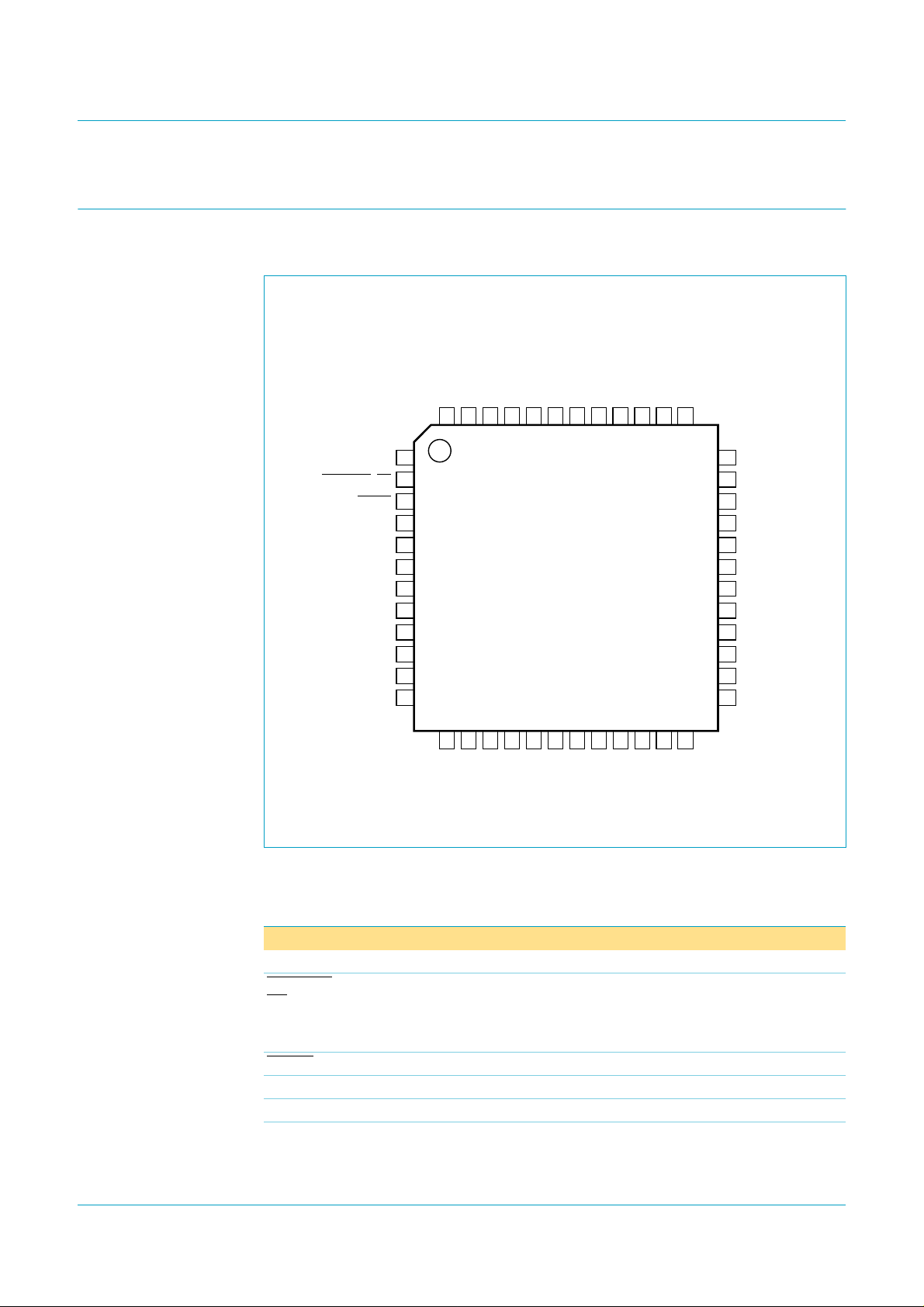
6. Pinning information
6.1 Pinning
dth
ISP1501
Hi-Speed USB peripheral transceiver
RX_VALID/VP
RX_INACTIVE/VM
48
47
RESET
V
CCA1
DM
DP
V
CCA2
RPU
1
2
3
4
5
6
7
8
9
10
11
12
13
14
RREF
CLKOUT48
SUSPEND
TX_VALID/OE
AGND1
AGND2
MODE0
MODE1
Fig 2. Pin configuration LQFP48.
RX_BS_ERROR/RCV
TEST_J_K/VO
46
45
ISP1501BE
15
16
CCA3
V
CLKOUT30
TX_BS_EN/FSE0
44
17
XTAL2
TX_READY
43
18
XTAL1
CCD2
DGND2
V
41
20
DDIR
40
21
DATA0
RX_LAST_BYTE
39
22
DATA1
TX_LAST_BYTE
42
19
AGND3
DATA15
DATA14
38
24 37
23
DATA2
DATA3
36
35
34
33
32
31
30
29
28
27
26
25
MGT060
DATA13
DATA12
DATA11
DATA10
DATA9
DATA8
DGND1
V
CCD1
DATA7
DATA6
DATA5
DATA4
6.2 Pin description
Table 2: Pin description
CCA1
[1]
Pin Type Description
2 I pin function depends on operating mode (see Table 3):
State = 0, 1 — output enable for FS transceiver
State = 2, 3 — transmission valid flag for HS transceiver
[2]
[2]
5 - analog supply voltage 1 (3.3 V)
resistor
© Koninklijke Philips Electronics N.V. 2002. All rights reserved.
Symbol
SUSPEND 1 I enables power saving mode for USB suspend state
TX_VALID/
OE
RESET 3 I reset input
AGND1 4 - analog ground 1 supply
V
DM 6 AI/O USB D− connection (analog) with integrated 45 Ω series
9397 750 10025
Product data Rev. 02 — 21 November 2002 4 of 40
Page 5

Philips Semiconductors
ISP1501
Hi-Speed USB peripheral transceiver
Table 2: Pin description
Symbol
[1]
Pin Type Description
…continued
DP 7 AI/O USB D+ connection (analog) with integrated 45 Ω series
resistor
V
CCA2
8 - analog supply voltage 2 (3.3 V)
RPU 9 AI connection for external pull-up resistor (1.5 kΩ±5%) on
USB D+; switched on via internal switch during the FS and
HS chirp states
AGND2 10 - analog ground2 supply
MODE0 11 I operating state and interface selection input 0; see Table 3
MODE1 12 I operating state and interface selection input 1; see Table 3
CLKOUT48 13 O 48 MHz clock output; clock is always running when input
SUSPEND is logic 0; see Section 17 on application of this
clock
RREF 14 AI connection for external reference resistor (12kΩ±1%) to
analog ground supply
CLKOUT30 15 O clock output for Hi-Speed USB digital interface (30 MHz);
clock is always running when input SUSPEND is logic 0
V
CCA3
16 - analog supply voltage 3 (3.3 V)
XTAL2 17 AO crystal oscillator output (12 MHz)
XTAL1 18 AI crystal oscillator input (12 MHz)
AGND3 19 - analog ground3 supply
DDIR 20 I selects direction of 16-bit data bus DATA[15:0]
DATA0 21 I/O data bit 0; bi-directional, slew rate controlled output (5 ns)
DATA1 22 I/O data bit 1; bi-directional, slew rate controlled output (5 ns)
DATA2 23 I/O data bit 2; bi-directional, slew rate controlled output (5 ns)
DATA3 24 I/O data bit 3; bi-directional, slew rate controlled output (5 ns)
DATA4 25 I/O data bit 4; bi-directional, slew rate controlled output (5 ns)
DATA5 26 I/O data bit 5; bi-directional, slew rate controlled output (5 ns)
DATA6 27 I/O data bit 6; bi-directional, slew rate controlled output (5 ns)
DATA7 28 I/O data bit 7; bi-directional, slew rate controlled output (5 ns)
V
CCD1
29 - digital supply voltage 1 (3.3 V)
DGND1 30 - digital ground 1 supply
DATA8 31 I/O data bit 8; bi-directional, slew rate controlled output (5 ns)
DATA9 32 I/O data bit 9; bi-directional, slew rate controlled output (5 ns)
DATA10 33 I/O data bit 10; bi-directional, slew rate controlled output (5 ns)
DATA11 34 I/O data bit 11; bi-directional, slew rate controlled output (5 ns)
DATA12 35 I/O data bit 12; bi-directional, slew rate controlled output (5 ns)
DATA13 36 I/O data bit 13; bi-directional, slew rate controlled output (5 ns)
DATA14 37 I/O data bit 14; bi-directional, slew rate controlled output (5 ns)
DATA15 38 I/O data bit 15; bi-directional, slew rate controlled output (5 ns)
RX_LAST_BYTE 39 O logic 0 — DATA[7:0] = valid data, DATA[15:8] = valid data
logic 1 — DATA[7:0] = valid data, DATA[15:8] = bit stuff
error byte
V
CCD2
9397 750 10025
Product data Rev. 02 — 21 November 2002 5 of 40
40 - digital supply voltage 2 (3.3 V)
© Koninklijke Philips Electronics N.V. 2002. All rights reserved.
Page 6

Philips Semiconductors
ISP1501
Hi-Speed USB peripheral transceiver
Table 2: Pin description
Symbol
DGND2 41 - digital ground 2 supply
TX_LAST_BYTE 42 I transmit last byte input; used in conjunction with
TX_READY 43 O transmit ready output; a logic 1 means ISP1501 is ready to
TX_BS_EN/FSE0 44 I pin function depends on operating state (see Table 3):
TEST_J_K/
VO
RX_BS_ERROR/
RCV
RX_INACTIVE/VM47 O pin function depends on operating state (see Table 3):
[1]
Pin Type Description
45 I pin function depends on operating state (see Table 3):
46 O pin function depends on operating state (see Table 3):
…continued
TX_BS_EN to indicate different handling of the upper and
lower data byte (see Table 7)
accept data on the next rising clock edge of CLKOUT30
State = 0, 1 — a logic 1 forces single-ended zero (SE0) for
FS transmitter
State = 2, 3 — a logic 1 enables bit stuffing for the HS
transmitter
State = 0, 1 — differential data for the FS transceiver input
State = 2, 3 — a logic 1 enables Hi-Speed USB test
modes TEST_J and TEST_K; it also disables bit stuffing
and NRZI for the HS receiver and transmitter
State = 0, 1 — differential data at D+/D− receiver output
State = 2, 3 — a logic 1 signals a bit stuff error on receive
data; the position of the erroneous byte is indicated by
RX_LAST_BYTE
State = 0, 1 — single-ended D− receiver output
State = 2, 3 — a logic 1 indicates HS line inactivity
RX_VALID/
VP
[1] Symbol names with an overscore (e.g. NAME) indicate active LOW signals.
[2] FS: full-speed (Original USB); HS: high-speed (Hi-Speed USB).
48 O pin function depends on operating state (see Table 3):
State = 0, 1 — single-ended D+ receiver output
State = 2, 3 — valid data on falling clock edge at
pin CLKOUT30
9397 750 10025
Product data Rev. 02 — 21 November 2002 6 of 40
© Koninklijke Philips Electronics N.V. 2002. All rights reserved.
Page 7

Philips Semiconductors
7. Functional description
The ISP1501 supports both full-speed (FS) and high-speed (HS) USB physical layer
for a Hi-Speed USB peripheral.
An adaptive termination circuit ensures a correct 45 Ω termination for DP and DM.
Calibration is done at power-on and after any operating state change.
An internal bandgap reference circuit is used for generating the driver current and the
biasing of the analog circuits. This circuit requires an external precision resistor
(12 kΩ±1%) to analog ground.
A PLL oscillator using a 12 MHz crystal generates the internal clock of 480 MHz.
Fromthis signal, 30 MHz and 48 MHz clocks are derived for external use (availableat
pins CLKOUT30 and CLKOUT48, respectively).
An internal power-on-reset (POR) circuit monitors the digital supply and is used to
start all circuits in the correct mode. An external reset can be applied via pin RESET.
7.1 Full-speed (FS) transceiver
ISP1501
Hi-Speed USB peripheral transceiver
The full-speed (FS) transceiver interface is a serial interface. Access to this interface
requires pins MODE1 and MODE0 to be set to either the disconnect state or the
full-speed (FS) state. Bit stuffing/de-stuffing and NRZI encoding/decoding must be
implemented on the external ASIC.
When pins MODE1 and MODE0 are in the disconnect or FS states, the FS
transceiver is active and follows the protocol as specified in Table 5. The only
difference between the disconnect and FS states is that the RPU resistor is
disconnected when MODE[1:0] is in the disconnect state whereas the RPU resistor is
connected to the DP line when MODE[1:0] is in the FS state.
To transmit FS USB traffic, pin OE is asserted by holding it at logic 0 (LOW) to enable
the transmit driver.The USB bus will be driven to the USB bus state that corresponds
to the logic conditions of FSE0 and VO. A logic 1 (HIGH) on pin FSE0 forces a USB
SE0 bus state in which both the DP and DM lines are held to a voltage less than
V
OL(max)
(see Table 13), regardless of VO.To force a USB J-state on the bus, FSE0 is
de-asserted (set to logic 0) and VO is asserted (set to logic 1). The DP line will be
held to a voltage greater than V
a voltage less than V
OL(max)
.
OH(min)
(see Table 13), and the DM line will be held to
To receive the FS USB traffic, the transmit driver needs to be disabled by the
de-asserted pin OE by holding it at logic 1. VP and VM always reflect the state of
DP and DM, respectively. An FS J-state (DP > V
bus will assert VP, de-assert VM and assert RCV. An FS K-state (DM > V
DP<V
SE0 on the USB bus (DP and DM < V
) on the USB bus will de-assert VP, assert VM and de-assert RCV. An
IL(max)
) will set VP and VM to LOW.RCV will be
IL(max)
IH(min)
and DM < V
IL(max)
) on the USB
and
IH(min)
held in the same state as it was just before the SE0 condition occurred. In the
suspend mode (SUSPND = HIGH), the differential receiver is inactive and output
RCV is always LOW. Out-of-suspend (‘K’) signalling is detected via the single-ended
receivers VP and VM. During suspend, the (D+, D-) lines are still driven to their
9397 750 10025
Product data Rev. 02 — 21 November 2002 7 of 40
© Koninklijke Philips Electronics N.V. 2002. All rights reserved.
Page 8

Philips Semiconductors
intended states without slew-rate control. This is permitted because driving during
suspend is used to signal remote wake-up by driving a ‘K’ signal (one transition from
idle to the ‘K’ state) for a period of 1 to 15 ms.
7.2 High-speed (HS) transceiver—transmit logic
The high-speed (HS) transceiver interface uses a 16-bit parallel bi-directional data
interface. This HS module incorporates bit stuffing/de-stuffing and
Non-Return-to-Zero-Inverted (NRZI) encoding/decoding logic. Access to the HS
interface requires MODE[1:0] to be set to either the high-speed (HS) state or the
high-speed (HS) chirp state.
When MODE[1:0] pins are in the HS or HS chirp states, the HS transceiver is active
and follows the protocol as specified in Section 10.1, Section 10.2 and Section 10.3.
One difference between the HS and HS chirp states is that the RPU resistor is
disconnected when MODE[1:0] is in the HS state whereas the RPU resistor is
connected to the DP line when MODE[1:0] is in the HS chirp state. Another difference
between the HS and HS chirp state is that the 45 Ω terminations are disabled from
the DP and DM lines in the HS chirp state.
ISP1501
Hi-Speed USB peripheral transceiver
The 16-bit data bus is a bi-directional bus. Pin DDIR must be set to logic 1 for
clocking data into the 16-bit DATA[15:0] bus so that the payload is transmitted from
the device to the host. If pin DDIR is set to logic 0, the 16-bit data bus is an output to
the external ASIC. Any payload transferred from the host/hub to the transceiver is
clocked out into the 16-bit data bus.
The transmit data is clocked on the rising edge of the 30 MHz clock output
(CLKOUT30). All the handshake signals (TX_LAST_BYTE, TX_BS_EN and
TX_VALID) are latched at the same time. These signals conform to the same set-up
and hold times as specified in Section 17.1. Each set of latched data, including the
16-bit data bus and handshake signals, are qualified if TX_VALID and TX_READY
are asserted during latching. TX_READY transitions take place on the falling edge of
the 30 MHz clock output.
For normal HS transmit, TEST_J_K is set to logic 0. The HS logic will process the
16-bit data with the latched TX_LAST_BYTE and TX_BS_EN signals according to
Table 7, and the processed data is serially driven on the USB bus in HS signaling.
When TEST_J_K is set to logic 1, the TX_BS_EN signal is ignored. The 16-bit input
data will be serially driven on the bus in HS signaling with the NRZI and bit-stuffing
disabled.
7.3 High-speed (HS) transceiver—receive logic
For receiving high-speed (HS) USB signals, the incoming differential signal from the
USB cable is amplified before it is fed into a sampler circuit. In the normal receive
mode, TEST_J_K is set to logic 0 and the over-sampled serial data is NRZI decoded
and bit de-stuffed before being converted to 16-bit parallel words. The 16-bit data and
other handshake signals (RX_BS_ERROR, RX_LAST_BYTE and RX_VALID) are
latched on the falling edge of CLKOUT30 in accordance with the timings as specified
in Table 18.
9397 750 10025
Product data Rev. 02 — 21 November 2002 8 of 40
© Koninklijke Philips Electronics N.V. 2002. All rights reserved.
Page 9

Philips Semiconductors
When TEST_J_K is set to logic 1, the sampled data from the differential amplifier will
not be NRZI decoded and bit de-stuffed. All serial HS USB signals are
passed-through and converted to 16-bit data on the parallel data bus. The handshake
signals (RX_BS_ERROR, RX_LAST_BYTE and RX_VALID) are invalid.
7.4 High-speed (HS) transceiver—periphery circuit
To maintain a constant current driver for high-speed (HS) transmit and biasing of
other analog circuits, an internal bandgap reference circuit and RREF resistor are
used to form the reference current. This circuit requires an external precision resistor
(12 kΩ±1%) from pin RF to the analog ground. A pull-up resistor of 1.5 kΩ±5%
must be connected between pin RPU and V
of less than ±500 ppm must be used between pins XTAL1 and XTAL2. Alternatively,
an input clock (3.3 V, 12 MHz clock ±500 ppm, duty cycle between 40 and 60%) can
also be used to drive pin XTAL1 (pin XTAL2 is left open).
8. Operating states
ISP1501
Hi-Speed USB peripheral transceiver
. A 12 MHz crystal with an accuracy
CCA3
8.1 Interface and state selection
The MODE1 and MODE0 pins control the operating states of the ISP1501 and select
the appropriate function of multiplexed pins (see Table 3).
Table 3: Interface selection
MODE[1:0] State State name Pin Function
00 0 Disconnect 2
44 FSE0
45 VO
46 RCV
47 VM
48 VP
01 1 Full-speed (FS) 2
44 FSE0
45 VO
46 RCV
47 VM
48 VP
10 2 High-speed (HS) 2
44 TX_BS_EN
45 TEST_J_K
46 RX_BS_ERROR
47 RX_INACTIVE
48 RX_VALID
OE
OE
TX_VALID
9397 750 10025
Product data Rev. 02 — 21 November 2002 9 of 40
© Koninklijke Philips Electronics N.V. 2002. All rights reserved.
Page 10

Philips Semiconductors
ISP1501
Hi-Speed USB peripheral transceiver
Table 3: Interface selection
…continued
MODE[1:0] State State name Pin Function
11 3 High-speed (HS)
chirp
2 TX_VALID
44 TX_BS_EN
45 TEST_J_K
46 RX_BS_ERROR
47 RX_INACTIVE
48 RX_VALID
8.2 State transitions
A Hi-Speed USB peripheral handles more than one electrical state under the USB
specification. The ISP1501 accommodates the various states through the MODE[1:0]
input pins. Table 4 summarizes the operating states.
Table 4: Operating states
State State name Description
0 Disconnect Legacy (full-speed) SIE interface; FS transceiver
enabled; pull-up resistor on pin RPU disconnected
1 Full-speed (FS) Legacy (full-speed) SIE interface; FS transceiver
enabled; full-speed slew rate selected; pull-up resistor
on pin RPU connected to pin DP
2 High-speed (HS) High-speed SIE interface; HS transceiver enabled;
FS transceiver on permanent SE0 to provide 45 Ω
termination; pull-up resistor on pin RPU disconnected
3 High-speed (HS) chirp High-speed SIE interface; HS transceiver enabled;
FS transceiver disabled; pull-up resistor on pin RPU
connected to pin DP
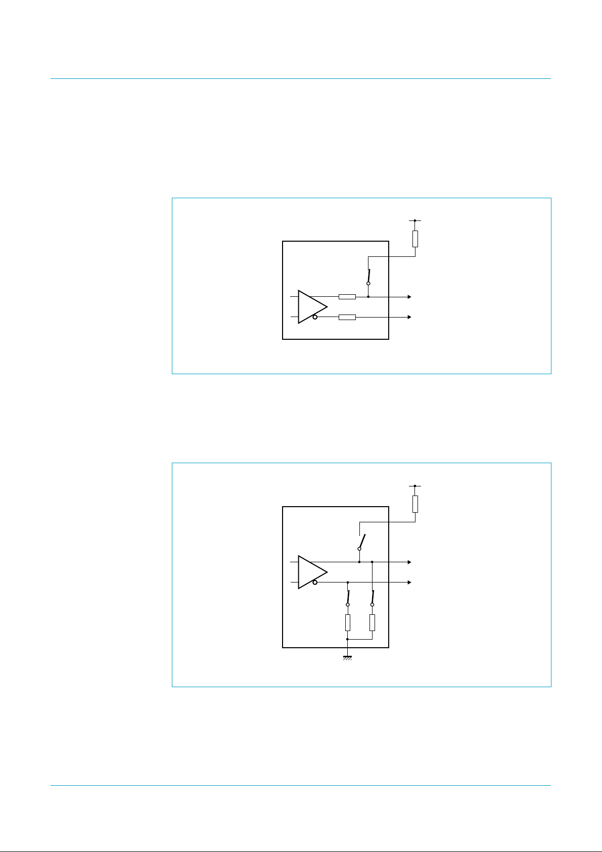
8.2.1 Disconnect state
In the disconnect state (MODE[1:0] = 00), an external pull-up resistor on pin RPU is
not connected to the DP line. The FS transceiver is enabled, and the legacy (Original
USB) SIE interface is active (see Figure 3).
3.3 V
1.5 kΩ
± 5%
RPU
9
ISP1501
45 Ω
45 Ω
FS driver
Fig 3. Disconnect state.
9397 750 10025
Product data Rev. 02 — 21 November 2002 10 of 40
004aaa039
7
DP
DM
6
© Koninklijke Philips Electronics N.V. 2002. All rights reserved.
Page 11
Philips Semiconductors
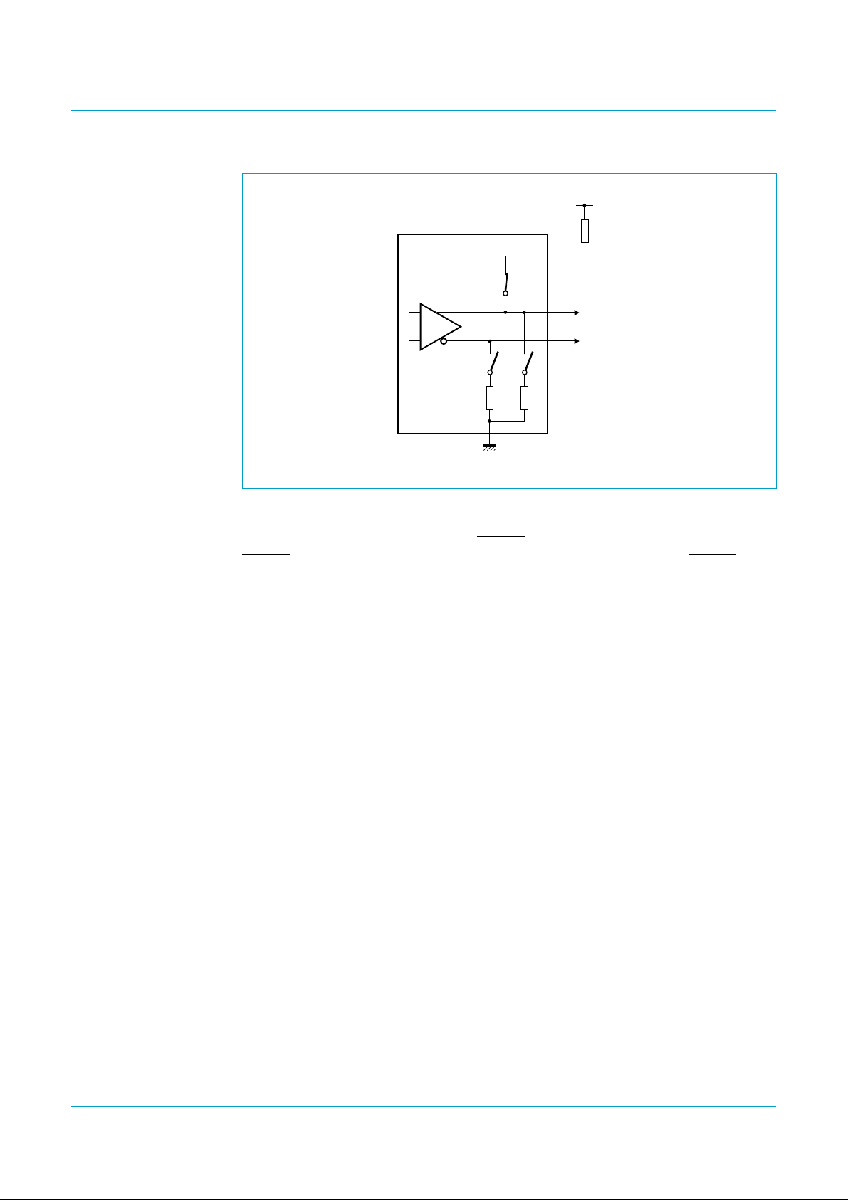
8.2.2 Full-speed (FS) state
In the full-speed (FS) state (MODE[1:0] = 01), an external pull-up resistor of
1.5 kΩ±5% is required on the DP line. This is implemented via the RPU resistor.The
RPU resistor is internally connected to the DP line. The FS transceiver is enabled,
and the legacy (Original USB) SIE interface is active (see Figure 4).
ISP1501
ISP1501
Hi-Speed USB peripheral transceiver
3.3 V
1.5 kΩ
± 5%
RPU
9
Fig 4. Full-speed state.
8.2.3 High-speed (HS) state
In the high-speed (HS) state, internal 45 Ω resistors on the DP and DM lines are
connected to the ground. The pull-up resistor is disconnected. The HS transceiver is
enabled, and the parallel interface and the HS-handshake signals are used (see
Figure 5).
FS driver
ISP1501
HS current
driver
45 Ω
45 Ω
004aaa052
7
DP
DM
6
3.3 V
1.5 kΩ
± 5%
RPU
9
7
DP
DM
6
45 Ω45 Ω
004aaa041
Fig 5. High-speed state.
8.2.4 High-speed (HS) chirp state
In the high-speed (HS) chirp state, 45 Ω terminations are disabled from the
DP and DM lines. The pull-up resistor is connected on the DP line. The
HS transceiveris enabled, and the parallel interface and HS handshake signals are in
use (see Figure 6).
9397 750 10025
Product data Rev. 02 — 21 November 2002 11 of 40
© Koninklijke Philips Electronics N.V. 2002. All rights reserved.
Page 12
Philips Semiconductors
Fig 6. High-speed chirp state.
ISP1501
HS current
driver
ISP1501
Hi-Speed USB peripheral transceiver
3.3 V
1.5 kΩ
± 5%
RPU
9
7
DP
DM
6
45 Ω45 Ω
004aaa040
8.3 Reset
The output clocks are affected by pin RESET and may show a momentary change at
RESET. The ASIC may not transmit or receive data while the ISP1510 RESET is
driven LOW.
9397 750 10025
Product data Rev. 02 — 21 November 2002 12 of 40
© Koninklijke Philips Electronics N.V. 2002. All rights reserved.
Page 13

Philips Semiconductors
9. Full-speed functionality
OE
VO
FSE0
RCV
VM
VP
ISP1501
Hi-Speed USB peripheral transceiver
3.3 V
1.5 kΩ
(1)
2
ISP1501
45 Ω
45
44
45 Ω
46
47
48
9
7
6
± 5%
RPU
DP
DM
MGT063
(1) Connected in FS state and HS chirp state.
Fig 7. Full-speed transceiver functional diagram
Table 5: Full-speed driving function
OE = logic 0
FSE0 VO VP VM Differential data (DP, DM)
0001 full-speed K state
0110 full-speed J state
1000 SE0
1100 SE0
Table 6: Full-speed receiving function
OE = logic 1
Differential input Single-ended input VP VM RCV
∆V=VDP− V
DM
V
DP
V
DM
∆V > 200 mV >2 V <0.8 V 1 0 1
∆V<−200 mV <0.8 V >2 V 0 1 0
|∆V|< 200 mV <0.8 V <0.8 V 0 0 RCV*
[1] When a logic 1 is applied at input SUSPEND, output RCV is always made logic 0.
[2] RCV* denotes the signal level on output RCV just before the SE0 state occurs. This level is kept
stable during the SE0 period.
[1]
[2]
9397 750 10025
© Koninklijke Philips Electronics N.V. 2002. All rights reserved.
Product data Rev. 02 — 21 November 2002 13 of 40
Page 14

Philips Semiconductors
10. High-speed functionality
ISP1501
Hi-Speed USB peripheral transceiver
SUSPEND
TEST_J_K
RX_BS_ERROR
RX_INACTIVE
RX_VALID
RX_LAST_BYTE
MODE1
DDIR
DATA15
to
DATA0
TX_READY
TX_VALID
TX_LAST_BYTE
TX_BS_EN
TEST_J_K
SUSPEND
MODE1, MODE0
16
2
1
45
46
47
48
39
12
20
38 to 31,
28 to 21
43
2
42
44
45
1
12, 11
MUX
shift
enable
ELASTIC FIFO
REGISTER
16-BIT TRANSMIT
REGISTER
16-BIT RECEIVE
LSB
BIT STUFFING
TRANSMIT LOGIC
RECEIVE LOGIC
PLL
NRZI ENCODER
sampling clock
NRZI enableBS enable
squelch
NRZI disableBS disable
NRZI DECODERBIT DE-STUFFING
sampling clock
HS data
HS drive enable
HS current source enable
sampling clock
ISP1501
squelch
detection
circuit
HS differential
receiver
HS current
driver
3.3 V
1.5 kΩ
(2)
± 5%
RPU
9
7
DP
6
DM
(1)
(1)
45
45
Ω
Ω
MGT341
(1) Implemented as part of the FS transceiver.
(2) Connected in FS state and HS chirp state.
Fig 8. High-speed transceiver functional diagram.
10.1 High-speed transmit
The ISP1501 must be set in high-speed state by setting MODE[1:0] = 02H.
High-speed data propagate to the DP and DM pins when the 16-bit input data bus is
driven. Driving pin DDIR to logic 1 switches the 16-bit data bus to input mode.
All data packets start with a 4-byte SYNC pattern and end with either a 1-byte or a
5-byte EOP (End of Packet). The SYNC pattern is a 32-bit pattern of KJKJKJKJ
KJKJKJKJ KJKJKJKJ KJKJKJKK, which is to be sent by the SIE as 0000H, 8000H to
the input. For a 1-byte EOP the HS pattern is generated with FEH. The 5-byte EOP
starts with FEH, followed by four bytes of FFH.
Remark: All 16-bit data are sent LSB first.
When bit stuffing or the EOP finishes on an 8-bit boundary, the TX_BS_EN and
TX_LAST_BYTE determine the behavior of the ISP1501 is shown in Table 7.
9397 750 10025
Product data Rev. 02 — 21 November 2002 14 of 40
© Koninklijke Philips Electronics N.V. 2002. All rights reserved.
Page 15

Philips Semiconductors
Table 7: High-speed transmit conditions
TX_LAST_BYTE TX_BS_EN Condition
ISP1501
Hi-Speed USB peripheral transceiver
0 0 high and low bytes are both sent without bit stuffing
0 1 high and low bytes are both sent with bit stuffing
1 0 low byte is sent without bit stuffing; high byte is ignored
1 1 low byte is sent with bit stuffing; high byte without bit
stuffing
CLKOUT30
TX_READY
TX_LAST_BYTE
TX_BS_EN
DATA[15:8
DATA[7:0
TX_VALID
SYNC
]
]
00H
00H 00H
Data0(H) Data1(H) Data2(H) Data3(H) FEH
80H
Data0(L) Data1(L) Data2(L) Data3(L) Data4(L)
(1)
(1) TX_READY is only de-asserted during a transmission if the internal FIFO is full.
Fig 9. HS transmit; single-byte EOP ending on 16-bit boundary.
CLKOUT30
TX_READY
TX_LAST_BYTE
TX_BS_EN
DATA[15:8
DATA[7:0
SYNC
]
]
00H
00H 00H
Data0(H) Data1(H) Data2(H) Data3(H) XX
80H
Data0(L) Data1(L) Data2(L) Data3(L) FEH
(1)
EOP
MGT064
EOP
TX_VALID
MGT067
(1) TX_READY is only de-asserted during a transmission if the internal FIFO is full.
Fig 10. HS transmit; single-byte EOP ending on 8-bit boundary.
9397 750 10025
Product data Rev. 02 — 21 November 2002 15 of 40
© Koninklijke Philips Electronics N.V. 2002. All rights reserved.
Page 16

Philips Semiconductors
CLKOUT30
TX_READY
TX_LAST_BYTE
ISP1501
Hi-Speed USB peripheral transceiver
(1)
TX_BS_EN
DATA[15:8
DATA[7:0
TX_VALID
]
]
SYNC
00H
00H 00H
80H
Data0(H) Data1(H) Data2(H) Data3(H) Data4(H)
Data0(L) Data1(L) Data2(L) Data3(L) Data4(L)
(1) TX_READY is only de-asserted during a transmission if the internal FIFO is full.
Fig 11. HS transmit; 5-byte EOP ending on 8-bit boundary.
CLKOUT30
TX_READY
TX_LAST_BYTE
TX_BS_EN
DATA[15:8
DATA[7:0
SYNC
]
]
00H
00H 00H
Data0(H) Data1(H) Data2(H) Data3(H) Data4(H) FEH FFH FFH
80H
Data0(L) Data1(L) Data2(L) Data3(L) Data4(L) Data5(L)
(1)
FFH FFH
EOP
FEH
FFH FFH
EOP
FFH FFH
XX
MGT069
TX_VALID
MGT065
(1) TX_READY is only de-asserted during a transmission if the internal FIFO is full.
Fig 12. HS transmit; 5-byte EOP ending on 16-bit boundary
10.2 High-speed receive
When ISP1501 is in high-speed state (MODE[1:0] = 02H), setting input DDIR to
logic 0 allows the HS receiver to output data to the external 16-bit bus. As the length
of the incoming EOP is not fixed, RX_LAST_BYTE and RX_BS_ERROR are
encoded to differentiate between EOP arriving on an 8-bit or a 16-bit boundary.
RX_VALID qualifies the data part of USB high-speed traffic. The SYNC pattern bytes
are removed.
If the EOP arrives on the high byte, RX_VALID will qualify it, and RX_LAST_BYTE
will be asserted. With these, the SIE will know that an EOP has occurred and can
start deciphering the received packet.
If the EOP arrives on the low byte, RX_VALID goes LOW at the start of the EOP
cycle. RX_BS_ERROR must be polled to determine whether an EOP has occurred.
9397 750 10025
Product data Rev. 02 — 21 November 2002 16 of 40
© Koninklijke Philips Electronics N.V. 2002. All rights reserved.
Page 17

Philips Semiconductors
Table 8: High-speed receive conditions
RX_LAST_BYTE RX_BS_ERROR Condition
[1] This condition is only valid in the cycle immediately after pin RX_VALID goes LOW.
ISP1501
Hi-Speed USB peripheral transceiver
0 0 valid data on the high and low bytes; no bit stuff error
[1]
0
1 0 EOP on the high byte; valid data on the low byte
1 1 illegal
CLKOUT30
RX_LAST_BYTE
RX_BS_ERROR
DATA[15:8
[1]
1
]
EOP on the low byte
SYNC
Data0(H) Data1(H) Data2(H) Data3(H)
80H
EOP
FEH
DATA[7:0
RX_VALID
]
Data0(L) Data1(L) Data2(L) Data3(L) Data4(L)
00H
Fig 13. HS receive timing; single-byte EOP starting on the high byte.
CLKOUT30
RX_LAST_BYTE
RX_BS_ERROR
SYNC
DATA[15:8
DATA[7:0
RX_VALID
]
]
Data0(H) Data1(H) Data2(H) Data3(H) XX
80H
Data0(L) Data1(L) Data2(L) Data3(L)
00H
EOP
FEH
Fig 14. HS receive timing; single-byte EOP starting on the low byte.
MGT070
MGT073
9397 750 10025
© Koninklijke Philips Electronics N.V. 2002. All rights reserved.
Product data Rev. 02 — 21 November 2002 17 of 40
Page 18

Philips Semiconductors
CLKOUT30
RX_LAST_BYTE
RX_BS_ERROR
SYNC
DATA[15:8
DATA[7:0
RX_VALID
]
]
Fig 15. HS receive timing; 5-bytes EOP starting on the low byte.
CLKOUT30
Data0(H) Data1(H) Data2(H) Data3(H) Data4(H)
80H
Data0(L) Data1(L) Data2(L) Data3(L) Data4(L)
00H
ISP1501
Hi-Speed USB peripheral transceiver
XX
FFH
FFH
EOP
FEH
FFH FFH
MGT075
TX_READY
TX_LAST_BYTE
TX_BS_EN
DATA[15:8
DATA[7:0
TX_VALID
SYNC
]
]
00H
00H 00H
Data0(H) Data1(H) Data2(H) Data3(H) Data4(H) FEH FFH FFH
80H
Data0(L) Data1(L) Data2(L) Data3(L) Data4(L) Data5(L)
(1)
Fig 16. HS receive timing; 5-bytes EOP starting on the high byte.
The SYNC pattern will not appear on the data bus as an RX_VALID qualified data.
The received SYNC value may differ from the expected 8000H.
The raw data is byte-aligned to the 16-bit data bus.
10.3 High-speed chirp
When the transceiver is configured to high-speed chirp state (MODE[1:0] = 03H), the
internal termination resistors on DP and DM are deactivated (no SE0 is applied by
the FS transceiver). Pin DP is connected to the pull-up resistor on pin RPU. No bit
stuffing or NRZI encoding is performed on the data, regardless of the state of
pin TX_BS_EN. The data is transmitted as soon as both TX_VALID and TX_READY
are asserted (see Figure 17).
EOP
FFH FFH
MGT065
9397 750 10025
© Koninklijke Philips Electronics N.V. 2002. All rights reserved.
Product data Rev. 02 — 21 November 2002 18 of 40
Page 19

Philips Semiconductors
ISP1501
Hi-Speed USB peripheral transceiver
handbook, full pagewidth
CLKOUT30
TX_READY
TX_VALID
DATA[15:0
DP/DM
HIGH
]
0000H
(1) Time interval controlled by the SIE.
Fig 17. HS chirp transmit timing.
For HS chirp reception, the 16-bit data bus is in the bypass mode.
In the HS chirp mode, the receiver behaves like a simple serial to parallel converter.
The transition on DP and DM may be mapped to anywhere within the 16-bit word
boundary. Therefore, the output may not contain all 0s or 1s for one cycle. The SIE
samples the 16-bit parallel data to check for the presence of extended JKJK states.
RX_BS_ERROR no longer reflects a bit stuff error. The RX_VALID signal is used to
qualify the data. The RX_INACTIVE signal is used in the HS chirp receive state.
40 to 60 µs
FFFFH 0000H FFFFH
(1)
MGT200
handbook, full pagewidth
CLKOUT30
RX_VALID
DP/DM
DATA[15:0
RX_INACTIVE
HS IDLE
]
Fig 18. HS chirp receive timing.
10.4 High-speed transmit path delay
The total transmit path maximum delay is 8 HS bit times at 480 MHz.
HS IDLE
40 to 60 µs
FFFFH0000H 0000H
MGT201
9397 750 10025
© Koninklijke Philips Electronics N.V. 2002. All rights reserved.
Product data Rev. 02 — 21 November 2002 19 of 40
Page 20

Philips Semiconductors
handbook, full pagewidth
480 MHz clock
CLKOUT30
ISP1501
Hi-Speed USB peripheral transceiver
DATA[15:0
TX_READY
TX_VALID
]
DP/DM
Fig 19. HS transmit path delay.
10.5 High-speed receive path delay
In the HS receive mode, the SYNC pattern is removed. As the preceding SYNC
pattern may be trimmed, the delay from the appearance of the first bit of the SYNC
pattern to the first valid data word on the DATA[15:0] bus is described here (see
Figure 20, tAtB and tC). The receive path delay is between 106 to 122 HS bit times.
However, to have an accurate measure of the bus turn-around time, the receive path
delay is measured from the data on the DP and DM pins to the actual equivalent data
on the 16-bit data bus (see Figure 20, tBand tC).
handbook, full pagewidth
480 MHz clock
8000H XXXX0000H
8 HS bit times
driver enabled
MGT076
CLKOUT30
00H 00H 00H 80H 80H 40H
DP/DM
106 to 122 HS bit times
DATA[15:0
RX_VALID
]
t
A
t
B
4080H
MGT202
t
C
Fig 20. HS receive path delay.
9397 750 10025
Product data Rev. 02 — 21 November 2002 20 of 40
© Koninklijke Philips Electronics N.V. 2002. All rights reserved.
Page 21

Philips Semiconductors
11. Clocking
The CLKOUT30 and CLKOUT48 pins are free running clocks at 30 MHz and 48 MHz,
respectively.
11.1 Power-up behavior
Both output clocks (CLKOUT30 and CLKOUT48) are held LOW (logic 0) at power-up
for a period of up to 8192 oscillator cycles before they are enabled.
The time during which these output clocks are blocked depends on the start-up time
of the external crystal. A total of 8192 oscillator clock ticks must be counted before
enabling the output clocks. Therefore, the minimum timing from power-up to the time
when CLKOUT30 and CLKOUT48 are available is 8192 x 83 ns = 680 µs.
11.2 Suspend behavior
When SUSPEND is driven from logic 0 to logic 1, output clocks will stop toggling
because the internal PLL and the external crystal will also enter a power-down state.
The clocks CLKOUT30 and CLKOUT48 can stop at either logic 0 or logic 1.
ISP1501
Hi-Speed USB peripheral transceiver
When SUSPEND is driven from logic 1 to logic 0, the external crystal and the PLL will
start again. However, there is no blocking of output clocks. CLKOUT30 and
CLKOUT48 may drift slightly from 30 MHz and 48 MHz, respectively until the PLL
locks up.
11.3 Reset behavior
A pin reset will force the digital circuit that generates 30 MHz and 48 MHz from the
HS PLL (480 MHz) to the initial state. Therefore, the output clock at 30 MHz and
48 MHz will be aligned after pin RESET is driven from logic 1 to logic 0 (falling edge).
During that one instance, the alignment causes the clock period to change.
9397 750 10025
Product data Rev. 02 — 21 November 2002 21 of 40
© Koninklijke Philips Electronics N.V. 2002. All rights reserved.
Page 22

Philips Semiconductors
12. Termination calibration
The on-chip termination is calibrated after power-up and mode change to provide
45 Ω±10% termination resistance. The ISP1501 must not transmit or receive data
during calibration.
12.1 Power-up behavior
This internal termination calibration occurs 21600 oscillator cycles after power-up.
Similar to the clock blocking mechanism, the exact timing depends on the external
crystal startup time. Therefore, the minimum timing from power-up to power-up
termination calibration is 21600 x 83 ns = 1.8 ms.
12.2 Suspend behavior
Pin SUSPEND does not cause any termination calibration.
12.3 Reset behavior
Pin RESET does not cause any termination calibration.
ISP1501
Hi-Speed USB peripheral transceiver
12.4 Mode change behavior
A termination calibration occurs 4 µs after a mode change and lasts for 2 µs.
RX_INACTIVE is asserted to facilitate calibration during this 2 µs period.
9397 750 10025
Product data Rev. 02 — 21 November 2002 22 of 40
© Koninklijke Philips Electronics N.V. 2002. All rights reserved.
Page 23

Philips Semiconductors
ISP1501
Hi-Speed USB peripheral transceiver
13. Limiting values
Table 9: Absolute maximum ratings
In accordance with the Absolute Maximum Rating System (IEC 60134).
Symbol Parameter Conditions Min Max Unit
V
CCA
V
CCD
V
I
I
lu
V
esd
T
stg
[1] Equivalent to discharging a 100 pF capacitor via a 1.5 kΩ resistor (Human Body Model).
analog supply voltage −0.5 +6.0 V
digital supply voltage −0.5 +4.6 V
input voltage −0.5 +6.0 V
latch-up current −1.8 V < VI< +5.4 V - 100 mA
electrostatic discharge voltage
[1]
ILI<1µA
pins DP, DM and
−4000 +4000 V
ground pins
other pins −2000 +2000 V
storage temperature −40 +125 °C
14. Recommended operating conditions
Table 10: Recommended operating conditions
Symbol Parameter Conditions Min Typ Max Unit
V
V
V
V
CCA
CCD
I
I(AI/O)
analog supply voltage 3.0 3.3 3.6 V
digital supply voltage 3.0 3.3 3.6 V
input voltage 0 - V
input voltage on analog I/O pins DP
0 - 3.6 V
CCD
V
and DM
T
amb
ambient temperature −40 - +85 °C
15. Static characteristics
Table 11: Static characteristics: supply pins
V
CCA=VCCD
Symbol Parameter Conditions Min Typ Max Unit
I
CC
I
CC(susp)
= 3.0 to 3.6 V; V
operating supply
current
suspend supply
current
AGND=VDGND
=0V; T
full-speed transmitting and receiving at
=−40 to+85°C; unless otherwise specified.
amb
-25-mA
12 MHz; 50 pF load on pins DP and DM
high-speed receiving at 480 MHz - 60 - mA
high-speed transmitting at 480 MHz - 75 - mA
in suspend mode with resistor on pin RPU
- 100 - µA
disconnected
9397 750 10025
Product data Rev. 02 — 21 November 2002 23 of 40
© Koninklijke Philips Electronics N.V. 2002. All rights reserved.
Page 24

Philips Semiconductors
ISP1501
Hi-Speed USB peripheral transceiver
Table 12: Static characteristics: digital pins
V
CCA=VCCD
Symbol Parameter Conditions Min Typ Max Unit
Input levels
V
IL
V
IH
Output levels
V
OL
V
OH
Leakage current
I
LI
Table 13: Static characteristics: analog I/O pins DP and DM)
V
CCA=VCCD
Symbol Parameter Conditions Min Typ Max Unit
Original USB transceiver (FS)
Input levels (differential receiver)
V
DI
V
CM
Input levels (single-ended receivers)
V
IL
V
IH
V
hys
Output levels
V
OL
V
OH
Hi-Speed USB transceiver (HS)
Input levels (differential receiver)
V
HSSQ
V
HSDSC
V
HSDI
V
HSCM
Output levels
V
HSOI
V
HSOL
= 3.0 to 3.6 V; V
AGND=VDGND
=0V; T
=−40 to+85°C; unless otherwise specified.
amb
LOW-level input voltage - - 0.8 V
HIGH-level input voltage 2.0 - - V
LOW-level output voltage IOL= 100 µA - - 0.15 V
= 4 mA - - 0.4 V
I
OL
HIGH-level output voltage IOH= 100 µAV
= 4 mA V
I
OH
− 0.4 - - V
CCD
− 0.4 - - V
CCD
input leakage current - - ±1 µA
= 3.0 to 3.6 V; V
AGND=VDGND
differential input sensitivity |V
=0V; T
=−40 to+85°C; unless otherwise specified.
amb
I(DP)
− V
| 0.2 - - V
I(DM)
differential common mode voltage includes VDI range 0.8 - 2.5 V
LOW-level input voltage - - 0.8 V
HIGH-level input voltage 2.0 - - V
hysteresis voltage 0.4 - 0.7 V
LOW-level output voltage pull-up on DP;
= 1.5 kΩ to + 3.6 V
R
L
HIGH-level output voltage pull-down on DP, DM;
=15kΩ to GND
R
L
high-speed squelch detection
threshold (differential)
high-speed disconnect detection
threshold (differential)
high-speed differential input
squelch detected - - 100 mV
no squelch detected 150 - - mV
disconnect detected 625 - - mV
disconnect not detected - - 525 mV
|V
I(DP)
− V
| 300 - - mV
I(DM)
0 - 0.3 V
2.8 - 3.6 V
sensitivity
high-speed data signaling
−50 - +500 mV
common mode voltage range
high-speed idle level output
−10 - +10 mV
voltage (differential)
high-speed LOW-level output
−10 - +10 mV
voltage (differential)
9397 750 10025
Product data Rev. 02 — 21 November 2002 24 of 40
© Koninklijke Philips Electronics N.V. 2002. All rights reserved.
Page 25

Philips Semiconductors
ISP1501
Hi-Speed USB peripheral transceiver
Table 13: Static characteristics: analog I/O pins DP and DM)
V
CCA=VCCD
= 3.0 to 3.6 V; V
AGND=VDGND
=0V; T
=−40 to+85°C; unless otherwise specified.
amb
…continued
Symbol Parameter Conditions Min Typ Max Unit
V
HSOH
high-speed HIGH-level output
360 - 440 mV
voltage (differential)
V
CHIRPJ
V
CHIRPK
chirp-J output voltage (differential)
chirp-K output voltage (differential)
[1]
700 - 1100 mV
[1]
−900 - −500 mV
Leakage current
I
LZ
OFF-state leakage current - - ±1 µA
Capacitance
C
IN
transceiver capacitance pin to GND - - 20 pF
Resistance
Z
DRV2
driver output impedance for
steady-state drive
[2]
40.5 45 49.5 Ω
Hi-Speed USB and Original USB
Z
INP
input impedance 10 - - MΩ
Termination
V
TERM
termination voltage for pull-up
[3]
3.0 - 3.6 V
resistor on pin RPU
[1] HS termination resistor disabled, pull-up resistor connected. Only during reset, when both hub and device are high-speed capable.
[2] Includes internal matching resistors on both pins DP and DM. This tolerance range complies to Hi-Speed USB.
[3] In suspend mode the minimum voltage is 2.7 V.
16. Dynamic characteristics
Table 14: Dynamic characteristics: analog I/O pins (DP/DM)
V
CCA=VCCD
Symbol Parameter Conditions Min Typ Max Unit
Driver characteristics
Full-speed mode
t
FR
t
FF
FRFM differential rise/fall time
V
CRS
High-speed mode
t
HSR
t
HSF
Driver timing
Full-speed mode
t
PLH(drv)
t
PHL(drv)
9397 750 10025
Product data Rev. 02 — 21 November 2002 25 of 40
= 3.0 to 3.6 V; V
AGND=VDGND
=0V; T
=−40 to+85°C; unless otherwise specified.
amb
rise time CL= 50 pF; 10% to 90% of
− VOL|; see Figure 21
|V
OH
fall time CL= 50 pF; 90% to 10% of
− VOL|; see Figure 21
|V
OH
excluding the first transition
matching (t
output signal crossover
voltage
FR/tFF
)
from Idle state
excluding the first transition
from Idle state; see Figure 22
high-speed differential
rise time
high-speed differential
fall time
driver propagation delay
(VO, FSE0 to DP, DM)
LOW-to-HIGH; seeFigure 24 --15ns
HIGH-to-LOW; see Figure 24 --15ns
4 - 20 ns
4 - 20 ns
90 - 111.1 %
1.3 - 2.0 V
500 - - ps
500 - - ps
© Koninklijke Philips Electronics N.V. 2002. All rights reserved.
Page 26

Philips Semiconductors
ISP1501
Hi-Speed USB peripheral transceiver
Table 14: Dynamic characteristics: analog I/O pins (DP/DM)
V
CCA=VCCD
= 3.0 to 3.6 V; V
AGND=VDGND
=0V; T
=−40 to+85°C; unless otherwise specified.
amb
…continued
Symbol Parameter Conditions Min Typ Max Unit
t
PHZ
t
PLZ
t
PZH
t
PZL
driver disable delay
OE to DP, DM)
(
driver enable delay
OE to DP, DM)
(
High-speed mode (Template 1,
- driver waveform
requirements
Universal Serial Bus Specification Rev. 2.0
HIGH-to-OFF; see Figure 22 --10ns
LOW-to-OFF; seeFigure 22 --10ns
OFF-to-HIGH; see Figure 22 --15ns
OFF-to-LOW; see Figure 22 --15ns
)
eye pattern of Template 1;
[1]
see Figure 26 and Table 15
Receiver timing full-speed mode
Differential receiver
t
PLH(rcv)
t
PHL(rcv)
receiver propagation
delay (DP, DM to RCV)
LOW-to-HIGH; seeFigure 23 --15ns
HIGH-to-LOW; see Figure 23 --15ns
Single-ended receiver
t
PLH(se)
t
PHL(se)
single-ended propagation
delay (DP, DM to VP, VM)
LOW-to-HIGH; seeFigure 23 --15ns
HIGH-to-LOW; see Figure 23 --15ns
Receiver timing high-speed mode
Template 4,
- data source jitter and
Universal Serial Bus Specification Rev. 2.0
eye pattern of Template 4;
receiver jitter tolerance
see Figure 27 and Table 16
[1]
[1] Characterized only, not tested in production. Limits guaranteed by design.
2.7 V
logic input
tFR, t
V
OH
V
OL
LR
90%
10%
90%
tFF, t
10%
LF
V
MGT077
V
0 V
OH
differential
data lines
OL
1.5 V
t
PZH
t
PZL
V
CRS
Fig 21. Rise and fall times (FS and LS mode). Fig 22. Timing of OE to DP, DM.
2.0 V
differential
data lines
0.8 V
V
OH
logic output
V
OL
V
CRS
t
PLH(rcv)
t
PLH(se)
1.5 V
V
CRS
t
PHL(rcv)
t
PHL(se)
1.5 V
MGT079
2.7 V
logic input
0 V
V
OH
V
OL
differential
data lines
1.5 V
t
PLH(drv)
V
CRS
1.5 V
t
PHZ
t
PLZ
V
−0.3 V
OH
V
+0.3 V
OL
1.5 V
t
PHL(drv)
V
MGT080
CRS
MGT078
Fig 23. Timing of DP, DM to RCV, VP, VM. Fig 24. Timing of VO, FSE0 to DP, DM.
9397 750 10025
Product data Rev. 02 — 21 November 2002 26 of 40
© Koninklijke Philips Electronics N.V. 2002. All rights reserved.
Page 27

Philips Semiconductors
16.1 High-speed signals
High-speed USB signals are characterized using eye patterns. For measuring the eye
patterns 4 test points have been defined (see Figure 25). The
Specification Rev. 2.0
only Templates 1 and 4 are relevant.
ISP1501
Hi-Speed USB peripheral transceiver
Universal Serial Bus
defines the eye patterns in several ‘templates’. For ISP1501
TP1 TP2
traces
transceiver
hub circuit board
A
connector
Fig 25. Eye pattern measurement planes.
16.1.1 Template 1 (transmit waveform)
The eye pattern in Figure 26 defines the transmit waveform requirements for a hub
(measured at TP2) or a device without a captive cable (measured at TP3).
Remark: Captive cables have a vendor-specific connector to the peripheral
(hardwired or detachable) and a USB “A” connector on the other side. For hot
plugging, the vendor-specific connector must meet the same performance
requirements as a USB “B” connector.
The corresponding signal levels and timings are given in Table 15. Timings are given
as a percentage of the unit interval (UI), which represents the nominal bit duration
T
for a 480 Mbit/s transmission rate.
PERIOD
USB cable
MBL205
TP3 TP4
traces
B
connector
device circuit board
transceiver
MBL206
level 1
+400 mV
point 2point 1
0
−400 mV
level 2
differential
output
voltage
(mV)
600
500
400
300
200
100
0
−100
−200
−300
−400
−500
−600
0 100relative duration
point 3 point 4
point 5
(% of unit interval)
point 6
Fig 26. Template 1 eye pattern (transmit waveform).
9397 750 10025
Product data Rev. 02 — 21 November 2002 27 of 40
© Koninklijke Philips Electronics N.V. 2002. All rights reserved.
Page 28

Philips Semiconductors
Table 15: Template 1 eye pattern definition
Name Differential voltage on pins DP and DM
Level 1 +525
Level 2 −525
Point 1 0 7.5
Point 2 0 92.5
Point 3 +300 37.5
Point 4 +300 62.5
Point 5 −300 37.5
Point 6 −300 62.5
[1] In the unit interval following a transition.
[2] In all other cases.
16.1.2 Template 4 (receive waveform)
The eye pattern defined in Table 16 defines the receiver sensitivity requirements for a
hub (signal applied at test point TP2) or a device without a captive cable (signal
applied at test point TP3). The corresponding signal levels and timings are given in
Table 16. Timings are given as a percentage of the unit interval (UI), which represents
the nominal bit duration T
Hi-Speed USB peripheral transceiver
(mV)
[1]
[2]
+475
[1]
[2]
−475
for a 480 Mbit/s transmission rate.
PERIOD
ISP1501
Relative duration
(% of unit interval)
n.a.
n.a.
input
(mV)
600
500
400
300
200
100
0
−100
−200
−300
−400
−500
−600
0 100relative duration
point 3 point 4
point 1
point 5 point 6
(% of unit interval)
differential
voltage
Fig 27. Template 4 eye pattern (receive waveform).
point 2
MBL207
level 1
+400 mV
0
−400 mV
level 2
9397 750 10025
Product data Rev. 02 — 21 November 2002 28 of 40
© Koninklijke Philips Electronics N.V. 2002. All rights reserved.
Page 29

Philips Semiconductors
Table 16: Template 4 eye pattern definition
Name Differential voltage on pins DP and DM
Level 1 +575 n.a.
Level 2 −575 n.a.
Point 1 0 15
Point 2 0 85
Point 3 +150 35
Point 4 +150 65
Point 5 −150 35
Point 6 −150 65
17. Parallel digital interface timing
17.1 High-speed transmit timing
(mV)
ISP1501
Hi-Speed USB peripheral transceiver
Relative duration
(% of unit interval)
CLKOUT30
t
su3(HSTX)
DDIR
]
t
su0(HSTX)
t
su2(HSTX)
t
su1(HSTX)
t
su4(HSTX)
DATA[15:0
TX_VALID
TX_LAST _BYTE
TX_BS_EN
TX_READY
Fig 28. Parallel digital interface timing: high-speed transmit.
t
h3(HSTX)
t
h0(HSTX)
t
h2(HSTX)
t
h1(HSTX)
t
d0(HSTX)
MGT085
9397 750 10025
Product data Rev. 02 — 21 November 2002 29 of 40
© Koninklijke Philips Electronics N.V. 2002. All rights reserved.
Page 30

Philips Semiconductors
ISP1501
Hi-Speed USB peripheral transceiver
Table 17: High-speed transmit timing
CLKOUT30 duty cycle = 50%; see Figure 28.
Symbol Parameter Conditions Min Typ Max Unit
t
su3(HSTX)
t
h3(HSTX)
t
su0(HSTX)
t
h0(HSTX)
t
su2(HSTX)
t
h2(HSTX)
t
su1(HSTX)
t
h1(HSTX)
t
su4(HSTX)
t
d0(HSTX)
data set-up time to rising
clock edge
data hold time after rising
clock edge
TX_VALID set-up time to
rising clock edge
TX_VALID hold time after
rising clock edge
TX_LAST_BYTE set-up
time to rising clock edge
TX_LAST_BYTE hold time
after rising clock edge
TX_BS_EN set-up time to
rising clock edge
TX_BS_EN hold time after
rising clock edge
DDIR switching time before
rising clock edge
TX_READY output delay
after falling clock edge
6.6 - - ns
0.1 - - ns
6.6 - - ns
0.1 - - ns
6.6 - - ns
0.1 - - ns
6.6 - - ns
0.1 - - ns
11--ns
- - 6.9 ns
17.2 High-speed receive timing
CLKOUT30
t
d0(HSRX)
DDIR
]
t
d1(HSRX)
t
d2(HSRX)
t
d3(HSRX)
t
su4(HSRX)
DATA[15:0
RX_VALID
RX_LAST _BYTE
RX_BS _ERROR
Fig 29. Parallel digital interface timing: high-speed receive.
MGT086
9397 750 10025
Product data Rev. 02 — 21 November 2002 30 of 40
© Koninklijke Philips Electronics N.V. 2002. All rights reserved.
Page 31

Philips Semiconductors
ISP1501
Hi-Speed USB peripheral transceiver
Table 18: High-speed receive timing
CLKOUT30 duty cycle = 50%; see Figure 29.
Symbol Parameter Conditions Min Typ Max Unit
t
d0(HSRX)
received data output delay
- - 6.8 ns
after falling clock edge
t
d1(HSRX)
RX_VALID delay after falling
- - 6.8 ns
clock edge
t
d2(HSRX)
RX_LAST_BYTE delayafter
- - 6.8 ns
falling clock edge
t
d3(HSRX)
RX_BS_ERROR delay after
- - 6.8 ns
falling clock edge
t
su4(HSRX)
DDIR switching time after
--11ns
rising clock edge
18. Application information
DATA15 to DATA0
16
CLKOUT30
RX_LAST_BYTE
RX_VALID/VP
RX_INACTIVE/VM
RX_BS_ERROR/RCV
TX_READY
TX_BS_EN/FSE0
TX_VALID/OE
TX_LAST_BYTE
TEST_J_K/VO
SUSPEND
2
MODE0, MODE1
12 kΩ
(1%)
DDIR
RESET
RREF
38 to 31,
28 to 21
20
15
39
48
47
46
43
44
2
42
45
3
1
11, 12
14
ISP1501
5, 8, 16
29, 40
4, 10, 19
30, 41
MGT061
DP
7
DM
6
RPU
9
XTAL1
18
XTAL2
17
V
CCA1
V
CCD1
AGND1 to AGND3
DGND1, DGND2
CLKOUT48
13
1.5 kΩ ± 5%
12 MHz
to V
CCA3
, V
CCD2
(1)
33 Ω
3.3 V
22 pF
3.3 V
3
2
3
2
22 pF
10 pF
DGND1
(1) The 48 MHz output clock might cause EMC problems unless care is taken during PCB design. If this clock is not used in the
ASIC, leavethispinunconnected to the PCB. Connect a 33 Ω series resistor and a 10 pF capacitor to this pin if it is used in the
ASIC.
Fig 30. Application diagram.
9397 750 10025
Product data Rev. 02 — 21 November 2002 31 of 40
© Koninklijke Philips Electronics N.V. 2002. All rights reserved.
Page 32

Philips Semiconductors
19. Test information
ISP1501
Hi-Speed USB peripheral transceiver
handbook, halfpage
D.U.T.
1.5 kΩ ± 5%
RPU
test point
DP/DM
(1)
3.3 V
(2)
C
L
(1) Internally connected to pin DP; FS operating state (see Table 4).
(2) CL=50pF forFS.
Fig 31. FS test circuit.
handbook, halfpage
D.U.T.
test point
Fig 32. Load for VM, VP and RCV in FS mode.
test supply
voltage
V
CCA
DP
D.U.T.
DM
AGND
143 Ω
15.8 Ω
15.8 Ω
143 Ω
25 pF
MGT082
15 kΩ
MGT081
50 Ω coax
50 Ω coax
+
(1) (2)
−
MBL204
(1) Transmitter: connected to 50 Ω inputs of a high-speed differential oscilloscope.
(2) Receiver: connected to 50 Ω outputs of a high-speed differential data generator.
Fig 33. High-speed transmitter/receiver test circuit.
9397 750 10025
Product data Rev. 02 — 21 November 2002 32 of 40
© Koninklijke Philips Electronics N.V. 2002. All rights reserved.
Page 33

Philips Semiconductors
20. Package outline
ISP1501
Hi-Speed USB peripheral transceiver
LQFP48: plastic low profile quad flat package; 48 leads; body 7 x 7 x 1.4 mm
c
y
X
36
37
pin 1 index
48
25
Z
24
E
e
w M
b
p
13
A
H
E
E
A
2
A
SOT313-2
(A )
A
1
L
3
θ
L
p
1
e
DIMENSIONS (mm are the original dimensions)
A
UNIT
mm
Note
1. Plastic or metal protrusions of 0.25 mm maximum per side are not included.
OUTLINE
VERSION
SOT313-2 MS-026136E05
A1A2A3bpcE
max.
0.20
0.05
1.45
1.35
IEC JEDEC EIAJ
1.60
b
p
0.25
w M
D
H
D
0.27
0.17
12
Z
D
B
0 2.5 5 mm
(1)
(1) (1)(1)
D
7.1
0.18
0.12
7.1
6.9
6.9
REFERENCES
v M
v M
scale
eHELL
H
9.15
0.5
8.85
detail X
A
B
Zywv θ
Z
0.95
0.55
D
E
0.95
0.55
ISSUE DATE
99-12-27
00-01-19
o
7
o
0
0.75
0.45
p
0.12 0.10.21.0
EUROPEAN
PROJECTION
D
9.15
8.85
Fig 34. Package outline.
9397 750 10025
Product data Rev. 02 — 21 November 2002 33 of 40
© Koninklijke Philips Electronics N.V. 2002. All rights reserved.
Page 34

Philips Semiconductors
21. Soldering
21.1 Introduction to soldering surface mount packages
This text gives a very brief insight to a complex technology. A more in-depth account
of soldering ICs can be found in our
Packages
There is no soldering method that is ideal for all surface mount IC packages. Wave
soldering can still be used for certain surface mount ICs, but it is not suitable for fine
pitch SMDs. In these situations reflow soldering is recommended.
21.2 Reflow soldering
Reflow soldering requires solder paste (a suspension of fine solder particles, flux and
binding agent) to be applied to the printed-circuit board by screen printing, stencilling
or pressure-syringe dispensing before package placement.
Several methods exist for reflowing; for example, convection or convection/infrared
heating in a conveyor type oven. Throughput times (preheating, soldering and
cooling) vary between 100 and 200 seconds depending on heating method.
ISP1501
Hi-Speed USB peripheral transceiver
Data Handbook IC26; Integrated Circuit
(document order number 9398 652 90011).
Typical reflow peak temperatures range from 215 to 250 °C. The top-surface
temperature of the packages should preferable be kept below 220 °C for thick/large
packages, and below 235 °C small/thin packages.
21.3 Wave soldering
Conventional single wave soldering is not recommended for surface mount devices
(SMDs) or printed-circuit boards with a high component density, as solder bridging
and non-wetting can present major problems.
To overcome these problems the double-wave soldering method was specifically
developed.
If wave soldering is used the following conditions must be observed for optimal
results:
• Use a double-wave soldering method comprising a turbulent wave with high
upward pressure followed by a smooth laminar wave.
• For packages with leads on two sides and a pitch (e):
– larger than or equal to 1.27 mm, the footprint longitudinal axis is preferred to be
parallel to the transport direction of the printed-circuit board;
– smaller than 1.27 mm, the footprint longitudinal axis must be parallel to the
transport direction of the printed-circuit board.
The footprint must incorporate solder thieves at the downstream end.
• For packages with leads on four sides, the footprint must be placed at a 45° angle
to the transport direction of the printed-circuit board. The footprint must
incorporate solder thieves downstream and at the side corners.
9397 750 10025
Product data Rev. 02 — 21 November 2002 34 of 40
© Koninklijke Philips Electronics N.V. 2002. All rights reserved.
Page 35

Philips Semiconductors
During placement and before soldering, the package must be fixed with a droplet of
adhesive. The adhesive can be applied by screen printing, pin transfer or syringe
dispensing. The package can be soldered after the adhesive is cured.
Typical dwell time is 4 seconds at 250 °C. A mildly-activated flux will eliminate the
need for removal of corrosive residues in most applications.
21.4 Manual soldering
Fix the component by first soldering two diagonally-opposite end leads. Use a low
voltage (24 V or less) soldering iron applied to the flat part of the lead. Contact time
must be limited to 10 seconds at up to 300 °C.
When using a dedicated tool, all other leads can be soldered in one operation within
2 to 5 seconds between 270 and 320 °C.
21.5 Package related soldering information
Table 19: Suitability of surface mount IC packages for wave and reflow soldering
Package
BGA, LBGA, LFBGA, SQFP, TFBGA, VFBGA not suitable suitable
DHVQFN, HBCC, HBGA, HLQFP, HSQFP,
HSOP, HTQFP, HTSSOP, HVQFN, HVSON,
SMS
PLCC
LQFP, QFP, TQFP not recommended
SSOP, TSSOP, VSO not recommended
ISP1501
Hi-Speed USB peripheral transceiver
methods
[1]
[4]
, SO, SOJ suitable suitable
Soldering method
Wave Reflow
not suitable
[3]
[4][5]
[6]
suitable
suitable
suitable
[2]
[1] For more detailed information on the BGA packages refer to the
(AN01026); order a copy from your Philips Semiconductors sales office.
[2] All surface mount (SMD) packages are moisture sensitive. Depending upon the moisture content, the
maximum temperature (with respect to time) and body sizeofthepackage, there is a risk that internal
or external package cracks may occur due to vaporization of the moisture in them (the so called
popcorn effect). For details, refer to the Drypack information in the
Circuit Packages; Section: Packing Methods
[3] These packages are not suitable for wave soldering. On versions with the heatsink on the bottom
side, thesoldercannotpenetratebetween the printed-circuit board and the heatsink. On versionswith
the heatsink on the top side, the solder might be deposited on the heatsink surface.
[4] If wave soldering is considered, then the package must be placed at a 45° angle to the solder wave
direction. The package footprint must incorporate solder thieves downstream and at the side corners.
[5] Wave soldering is suitable for LQFP, QFP and TQFP packages with a pitch (e) larger than 0.8 mm; it
is definitely not suitable for packages with a pitch (e) equal to or smaller than 0.65mm.
[6] Wave soldering is suitable for SSOP and TSSOP packages with a pitch (e) equal to or larger than
0.65 mm; it is definitely not suitable for packages with a pitch (e) equal to or smaller than 0.5 mm.
9397 750 10025
Product data Rev. 02 — 21 November 2002 35 of 40
.
(LF)BGA Application Note
Data Handbook IC26; Integrated
© Koninklijke Philips Electronics N.V. 2002. All rights reserved.
Page 36

Philips Semiconductors
Hi-Speed USB peripheral transceiver
ISP1501
22. Revision history
Table 20: Revision history
Rev Date CPCN Description
02 20021121 Product data (9397 750 10025); supersedes Objective specification of ISP1501-01 of
July 14th, 2000.
Modifications:
• Globally changed USB 2.0 and USB 1.1 to Hi-Speed USB and Original USB,
respectively.
• Globally changed XI and XO to XTAL1 and XTAL2, respectively.
• Section 8.3: changed the second sentence.
• Section 12.4: changed the second sentence.
• Figure 28: changed RX_READY.
• Table 17: in the t
• Figure 30: added 33 Ω series resistor and 10 pF capacitor to CLKOUT48. Also modified
the table note.
• Table 2: updated the pin description for pin 13.
• Added Section 8.3.
• Added Section 12.
• Figure 30: added a figure note.
• Table 11 I
CC(susp)
• In Section 1, expanded USB.
• Globally changed BS_EN to TX_BS_EN.
• Globally changed the external precision resistor from 12.2 kΩ±1% to 12 kΩ±1%.
• Globally added ±5% to the external pull-up resistor at RPU.
• Globally made TX_VALID active LOW.
• Globally changed CLOCKOUT (pin 15) to CLKOUT30 and TEST (pin 13) to CLKOUT48.
• Made the following changes in Section 2:
– In the fifth and sixth features, changed USB to Hi-Speed USB
– In the seventh and eighth features, added for Hi-Speed USB data
– Added the feature 3.3 V or 5 V tolerant digital input interface
– Changed the feature on ESD protection.
• In Figure 1, moved the product title name “ISP1501” to the top right corner.
• Made the following changes in Table 2:
– Pin 9 description, added 1.5 kΩ±5% as the external pull-up resistor. In addition,
added HS chirp state at the end of the description
– Pin 13 description, changed to “48 MHz output clock; clock is always running when...”
– Changed the first statement in the description for pin 15
– Modified the pin description for pin 20
– Pin 39: modified the pin description
– Pin 42: modified the pin description
– Pin 43 description, changed it to ISP1501 to make the description clearer
parameter description, changed rising to falling.
d0(HSTX)
removed the max value and added typ value as 100 µA.
9397 750 10025
Product data Rev. 02 — 21 November 2002 36 of 40
© Koninklijke Philips Electronics N.V. 2002. All rights reserved.
Page 37

Philips Semiconductors
ISP1501
Hi-Speed USB peripheral transceiver
Table 20: Revision history
Rev Date CPCN Description
02 20021121 Product data (9397 750 10025); supersedes Objective specification of ISP1501-01 of
…continued
July 14th, 2000.
Modifications (continued):
• Made the following changes in Table 2
– Corrected typo for pin 44 (FES0 changed to FSE0). Also, changed the description for
State = 2, 3
– Pin 45 description, changed the description for State = 0, 1
– Pin 48 description: changed the description for State = 2, 3.
• Made the following changes in Section 7:
– Removed the first three paragraphs
– Added the first sentence “The ISP1501 supports both full-speed (FS) and high-speed
(HS) USB physical layer.”
– Swapped the second and third paragraph
– Added Section 7.1 through Section 7.4
• In Section 8.2 first paragraph, removed“and Figure 3 shows the state transition diagram.”
Also, removed paragraphs 2 through 7 and the state transition diagram.
• In Table 4, added “to provide 45 Ω terminations” to the state 2 description.
• Changed Section 8.3 to Section 8.2.1. Also, removed the second sentence and added
Figure 3.
• Added Section 8.2.2 through Section 8.2.4.
• In Figure 8, added transistors on the DP and DM lines. Added RPU on DP, added table
note 2 and changed the pin order from 11, 12 to 12, 11 for MODE1 and MODE0.
• In Section 10.1 second paragraph, rephrased the second sentence.
• In Table 7 and Table 8, changed “high and low byte” to “high and low bytes”.
• In Figure 11, changed the Hex value for DATA[7:0] from 80H to 00H.
• In Figure 12, changed the Hex value for DATA[7:0] from 80H to 00H.
• In Section 10.2:
– First paragraph: added the last sentence
– Third paragraph: rephrased the first sentence
– Second last paragraph: rephrased the second sentence
– Last paragraph: removed the last sentence.
• In Table 8, changed text in the second and fourth rows of the condition column.
• Changed figure title in Figure 13, Figure 14, Figure 15 and Figure 16.
• In Figure 17, added a figure note.
• In Section 10.3, changed content in the second paragraph.
• In Section 10.4 first sentence, changed 37 bits to 8 HS bit times. Also, changed the same
in Figure 19.
• In Figure 20, changed clock cycles to HS bit times.
• In Section 10.5, changed content in the second sentence. Added reference to Figure 20
in the two paragraphs. Also, added the last sentence to the first paragraph.
• In Figure 7, switched the location of the DP and DM lines. Also, added RPU on DP.
• In Table 6, added table notes 3 and 4.
9397 750 10025
Product data Rev. 02 — 21 November 2002 37 of 40
© Koninklijke Philips Electronics N.V. 2002. All rights reserved.
Page 38

Philips Semiconductors
ISP1501
Hi-Speed USB peripheral transceiver
Table 20: Revision history
Rev Date CPCN Description
02 20021121 Product data (9397 750 10025); supersedes Objective specification of ISP1501-01 of
…continued
July 14th, 2000.
Modifications (continued):
• Added Section 11.
• In Table 9, changed I
to <1 µA. Removed table note 2 and changed V
LI
esd
.
• In Table 11, added typical values in all rows and removed the maximum values.
• In Table 13, added the minimum value for V
OL
as 0.
• In Table 14, removed content related to the low-speed mode.
• Separated Figure 23 and Figure 24 from Figure 21 and Figure 22.
• In Table 17, changed the order of the timing symbols to match their order in Figure 28.
Also, changed the value of t
SU4(HSTX)
to 11 ns.
• Made the following changes to Figure 28:
–
TX_VALID: changed the symbols t
– TX_LAST_BYTE: changed t
– Changed the width of the CLKOUT30 signal.
SU2(HSTX
SU0(HSTX)
• In Figure 29, changed the symbol for DDIR from t
• In Table 18, changed the parameter text for t
and added 11 ns in the max field. Also, made t
and t
) and t
H0(HSTX)
SU0(HSRX)
SU4(HSRX)
SU4(HSRX)
H2(HSTX)
to t
SU0(HSTX)
to t
SU2(HSTX)
to t
SU4(HSRX)
, removed the value in the min field
as the last row.
and t
and t
H2(HSTX)
.
H0(HSTX)
• In Figure 30:
– Added 22 pF to XTAL1 and XTAL2
– Removed n.c. from pin 13
– Changed 12.2 kΩ±1% to 12 kΩ±1%.
• In Figure 31, changed the content of figure note 1. Also, added figure note 2.
01 20000714 Objective data; initial version.
9397 750 10025
Product data Rev. 02 — 21 November 2002 38 of 40
© Koninklijke Philips Electronics N.V. 2002. All rights reserved.
Page 39

Philips Semiconductors
23. Data sheet status
ISP1501
Hi-Speed USB peripheral transceiver
Level Data sheet status
I Objective data Development This data sheet contains data from the objective specification for product development. Philips
II Preliminary data Qualification This data sheetcontains data from thepreliminary specification.Supplementary datawill be published
III Product data Production This data sheet contains data from the product specification. Philips Semiconductors reserves the
[1] Please consult the most recently issued data sheet before initiating or completing a design.
[2] The product status of the device(s) described in this data sheet may have changed since this data sheet was published. The latest information is available on the Internet at
URL http://www.semiconductors.philips.com.
[3] For data sheets describing multiple type numbers, the highest-level product status determines the data sheet status.
[1]
Product status
24. Definitions
Short-form specification — The data in a short-form specification is
extracted from a full data sheet with the same type number and title. For
detailed information see the relevant data sheet or data handbook.
Limiting values definition — Limiting values given are in accordance with
the Absolute Maximum Rating System (IEC 60134). Stress above one or
more of the limiting values may cause permanent damage to the device.
These are stress ratings only and operation of the device at these or at any
other conditions above those given in the Characteristics sections of the
specification is not implied. Exposure to limiting values for extended periods
may affect device reliability.
Application information — Applications that are described herein for any
of these products are for illustrative purposes only. Philips Semiconductors
make no representation or warranty that such applications will be suitable for
the specified use without further testing or modification.
[2][3]
Definition
Semiconductors reserves the right to change the specification in any manner without notice.
at a laterdate. Philips Semiconductors reserves therightto change the specification without notice,in
order to improve the design and supply the best possible product.
right to make changesat any time in order to improve the design, manufacturingandsupply. Relevant
changes will be communicated via a Customer Product/Process Change Notification (CPCN).
customers using or selling these products for use in such applications do so
at their own risk and agree to fully indemnify Philips Semiconductors for any
damages resulting from such application.
Right to make changes — Philips Semiconductors reserves the right to
make changes in the products - including circuits, standard cells, and/or
software - described or contained herein in order to improve design and/or
performance. When the product is in full production (status ‘Production’),
relevant changes will be communicated via a Customer Product/Process
Change Notification (CPCN). Philips Semiconductors assumes no
responsibility or liability for the use of any of these products, conveys no
licence or title under any patent, copyright, or mask work right to these
products, andmakes norepresentations or warrantiesthat these productsare
free frompatent, copyright, or maskwork right infringement, unlessotherwise
specified.
26. Trademarks
25. Disclaimers
Life support — These products are not designed for use in life support
appliances, devices, or systems where malfunction of these products can
reasonably be expected to result in personal injury. Philips Semiconductors
Jaz — is a registered trademark of Iomega Corp.
Zip — is a registered trademark of Iomega Corp.
Contact information
For additional information, please visit http://www.semiconductors.philips.com.
For sales office addresses, send e-mail to: sales.addresses@www.semiconductors.philips.com. Fax: +31 40 27 24825
9397 750 10025
Product data Rev. 02 — 21 November 2002 39 of 40
© Koninklijke Philips Electronics N.V. 2002. All rights reserved.
Page 40

Philips Semiconductors
Contents
ISP1501
Hi-Speed USB peripheral transceiver
1 General description . . . . . . . . . . . . . . . . . . . . . . 1
2 Features . . . . . . . . . . . . . . . . . . . . . . . . . . . . . . . 1
3 Applications . . . . . . . . . . . . . . . . . . . . . . . . . . . . 2
4 Ordering information. . . . . . . . . . . . . . . . . . . . . 2
5 Block diagram . . . . . . . . . . . . . . . . . . . . . . . . . . 3
6 Pinning information. . . . . . . . . . . . . . . . . . . . . . 4
6.1 Pinning . . . . . . . . . . . . . . . . . . . . . . . . . . . . . . . 4
6.2 Pin description . . . . . . . . . . . . . . . . . . . . . . . . . 4
7 Functional description . . . . . . . . . . . . . . . . . . . 7
7.1 Full-speed (FS) transceiver . . . . . . . . . . . . . . . 7
7.2 High-speed (HS) transceiver—transmit logic . . 8
7.3 High-speed (HS) transceiver—receive logic. . . 8
7.4 High-speed (HS) transceiver—periphery circuit 9
8 Operating states. . . . . . . . . . . . . . . . . . . . . . . . . 9
8.1 Interface and state selection. . . . . . . . . . . . . . . 9
8.2 State transitions . . . . . . . . . . . . . . . . . . . . . . . 10
8.2.1 Disconnect state . . . . . . . . . . . . . . . . . . . . . . . 10
8.2.2 Full-speed (FS) state . . . . . . . . . . . . . . . . . . . 11
8.2.3 High-speed (HS) state . . . . . . . . . . . . . . . . . . 11
8.2.4 High-speed (HS) chirp state. . . . . . . . . . . . . . 11
8.3 Reset . . . . . . . . . . . . . . . . . . . . . . . . . . . . . . . 12
9 Full-speed functionality. . . . . . . . . . . . . . . . . . 13
10 High-speed functionality. . . . . . . . . . . . . . . . . 14
10.1 High-speed transmit . . . . . . . . . . . . . . . . . . . . 14
10.2 High-speed receive. . . . . . . . . . . . . . . . . . . . . 16
10.3 High-speed chirp . . . . . . . . . . . . . . . . . . . . . . 18
10.4 High-speed transmit path delay . . . . . . . . . . . 19
10.5 High-speed receive path delay . . . . . . . . . . . . 20
11 Clocking . . . . . . . . . . . . . . . . . . . . . . . . . . . . . . 21
11.1 Power-up behavior . . . . . . . . . . . . . . . . . . . . . 21
11.2 Suspend behavior. . . . . . . . . . . . . . . . . . . . . . 21
11.3 Reset behavior . . . . . . . . . . . . . . . . . . . . . . . . 21
12 Termination calibration . . . . . . . . . . . . . . . . . . 22
12.1 Power-up behavior . . . . . . . . . . . . . . . . . . . . . 22
12.2 Suspend behavior. . . . . . . . . . . . . . . . . . . . . . 22
12.3 Reset behavior . . . . . . . . . . . . . . . . . . . . . . . . 22
12.4 Mode change behavior . . . . . . . . . . . . . . . . . . 22
13 Limiting values. . . . . . . . . . . . . . . . . . . . . . . . . 23
14 Recommended operating conditions. . . . . . . 23
15 Static characteristics. . . . . . . . . . . . . . . . . . . . 23
16 Dynamic characteristics . . . . . . . . . . . . . . . . . 25
16.1 High-speed signals. . . . . . . . . . . . . . . . . . . . . 27
16.1.1 Template 1 (transmit waveform) . . . . . . . . . . . 27
16.1.2 Template 4 (receive waveform). . . . . . . . . . . . 28
17 Parallel digital interface timing. . . . . . . . . . . . 29
17.1 High-speed transmit timing. . . . . . . . . . . . . . . 29
17.2 High-speed receive timing . . . . . . . . . . . . . . . 30
18 Application information . . . . . . . . . . . . . . . . . 31
19 Test information. . . . . . . . . . . . . . . . . . . . . . . . 32
20 Package outline. . . . . . . . . . . . . . . . . . . . . . . . 33
21 Soldering . . . . . . . . . . . . . . . . . . . . . . . . . . . . . 34
21.1 Introduction to soldering surface mount
packages. . . . . . . . . . . . . . . . . . . . . . . . . . . . 34
21.2 Reflow soldering. . . . . . . . . . . . . . . . . . . . . . . 34
21.3 Wave soldering. . . . . . . . . . . . . . . . . . . . . . . . 34
21.4 Manual soldering . . . . . . . . . . . . . . . . . . . . . . 35
21.5 Package related soldering information. . . . . . 35
22 Revision history . . . . . . . . . . . . . . . . . . . . . . . 36
23 Data sheet status. . . . . . . . . . . . . . . . . . . . . . . 39
24 Definitions . . . . . . . . . . . . . . . . . . . . . . . . . . . . 39
25 Disclaimers . . . . . . . . . . . . . . . . . . . . . . . . . . . 39
26 Trademarks . . . . . . . . . . . . . . . . . . . . . . . . . . . 39
© Koninklijke Philips Electronics N.V. 2002.
Printed in The Netherlands
All rights are reserved. Reproduction in whole or in part is prohibited without the prior
written consent of the copyright owner.
The information presented in this document does not form part of any quotation or
contract, is believed to be accurate and reliable and may be changed without notice. No
liability will be accepted by the publisher for any consequence of its use. Publication
thereof does not convey nor imply any license under patent- or other industrial or
intellectual property rights.
Date of release: 21 November 2002 Document order number: 9397 750 10025
 Loading...