Philips ISP1362 Quick start guide

ISP1362
Single-chip Universal Serial Bus On-The-Go controller
Rev. 03 — 06 January 2004 Product data
1. General description
The ISP1362 is a single-chip UniversalSerial Bus (USB) On-The-Go (OTG)controller
integrated with the advanced Philips Slave Host Controller (PSHC) and the Philips
ISP1181B Device Controller (DC). The USB OTG controller is compliant with
On-The-Go Supplement to the USB 2.0 Specification Rev. 1.0a. The host and device
controllers are compliant with Universal Serial Bus Specification Rev. 2.0, supporting
data transfer at full-speed (12 Mbit/s) and low-speed (1.5 Mbit/s).
The ISP1362 has two USB ports: port 1 and port 2. Port 1 can be hardware
configured to function as a downstream port, an upstream port or an OTG port
whereas port 2 can only be used as a downstream port. The OTG port can switch
roles from host to peripheral, or from peripheral to host. The OTG port can become a
host through the Host Negotiation Protocol (HNP) as specified in the OTG
supplement.
A USB product with OTG capability can function either as a host or as a peripheral.
For instance, with this dual-role capability,a PersonalComputer (PC) peripheral such
as a printer may switch roles from a peripheral to a host for connecting to a digital
camera so that the printer can print pictures taken by the camera without using a PC.
When a USB product with OTG capability is inactive, the USB interface is turned off.
This feature has made OTG a technology well-suited for use in portable
devices—such as, Personal Digital Assistant (PDA), Digital Still Camera (DSC) and
mobile phone—in which power consumption is a concern. The ISP1362 is an OTG
controller designed to perform such functions.
2. Features
■ Complies fully with:
◆ Universal Serial Bus Specification Rev. 2.0
◆ On-The-Go Supplement to the USB 2.0 Specification Rev. 1.0a
■ Supports data transfer at full-speed (12 Mbit/s) and low-speed (1.5 Mbit/s)
■ Adapted from Open Host Controller Interface Specification for USB Release 1.0a
■ USB OTG:
◆ Supports Host Negotiation Protocol (HNP) and Session Request Protocol
(SRP) for OTG dual-role devices
◆ Provides status and control signals for software implementation of HNP and
SRP
◆ Provides programmable timers required for HNP and SRP
◆ Supports built-in and external source of V
◆ Output current of the built-in charge pump is adjustable by using an external
capacitor
BUS

Philips Semiconductors
■ USB host:
■ USB device:
■ Supports two USB ports: port 1 and port 2
■ Supports software-controlled connection to the USB bus (SoftConnect™)
■ Supports good USB connection indicator that blinks with traffic (GoodLink™)
■ Complies with USB power management requirements
■ Supports internal power-on and low-voltage reset circuit, with possibility of a
■ Supports operation over the extended USB voltage range (4.0 V to 5.5 V) with
■ High-speed parallel interface to most CPUs available in the market, such as
■ Supports Programmed I/O (PIO) or Direct Memory Access (DMA)
■ Supports ‘suspend’ and remote wake-up
■ Uses 12 MHz crystal or direct clock source with on-chip Phase-Locked Loop
■ Operates at +3.3 V power supply
■ Operating temperature range from −40 °Cto+85 °C
■ Available in 64-pin LQFP and TFBGA packages.
ISP1362
Single-chip USB OTG controller
◆ Supports integrated physical 4096 bytes of multiconfiguration memory
◆ Supports all four types of USB transfers: control, bulk, interrupt and
isochronous
◆ Supports multiframe buffering for isochronous transfer
◆ Supports automatic interrupt polling rate mechanism
◆ Supports paired buffering for bulk transfer
◆ Directly addressable memory architecture; memory can be updated on-the-fly
◆ Supports high performance USB interface device with integrated Serial
Interface Engine (SIE), buffer memory and transceiver
◆ Supports fully autonomous and multiconfiguration DMA operation
◆ Supports up to 14 programmable USB endpoints with 2 fixed control IN/OUT
endpoints
◆ Supports integrated physical 2462 bytes of multiconfiguration memory
◆ Supports endpoints with double buffering to increase throughput and ease
real-time data transfer
◆ Supports controllable LazyClock (110 kHz ± 50 %) output during ‘suspend’
◆ Port 1 can be configured to function as a downstream port, an upstream port
or an OTG port
◆ Port 2 can be used only as a downstream port
software reset
5 V tolerant I/O pads
Hitachi SH-3, Intel® StrongARM®, Philips XA, Fujitsu SPARClite®, NEC and
Toshiba MIPS, ARM7/9, Motorola DragonBall™ and PowerPC™ Reduced
Instruction Set Computer (RISC):
◆ 16-bit data bus
◆ 10 Mbyte/s data transfer rate between the microprocessor and ISP1362
(PLL) for low Electro-Magnetic Interference (EMI)
9397 750 12337
Product data Rev. 03 — 06 January 2004 2 of 150
© Koninklijke Philips Electronics N.V. 2004. All rights reserved.

Philips Semiconductors
3. Applications
The ISP1362 can be used to implement a dual-role USB device in any
application—USB host or USB peripheral—depending on the cable connection. If the
dual-role device is connected to a typical USB peripheral, it behaves like a typical
USB host. The dual-role device, however, can also be connected to a PC or any other
USB host and behave like a typical USB peripheral.
3.1 Host/peripheral roles
■ Mobile phone to/from:
■ Digital still camera to/from:
■ Printer to/from:
■ MP3 player to/from:
■ Oscilloscope to/from:
■ Personal digital assistant to/from:
ISP1362
Single-chip USB OTG controller
◆ Mobile phone: exchange contact information
◆ Digital still camera: e-mail pictures or upload pictures to the web
◆ MP3 player: upload, download and broadcast music
◆ Mass storage: upload and download files
◆ Scanner: scan business cards
◆ Digital still camera: exchange pictures
◆ Mobile phone: e-mail pictures, upload pictures to the web
◆ Printer: print pictures
◆ Mass storage: store pictures
◆ Digital still camera: print pictures
◆ Scanner: print scanned image
◆ Mass storage: print files stored in a device
◆ MP3 player: exchange songs
◆ Mass storage: upload and download songs
◆ Printer: print screen image
◆ Personal digital assistant: exchange files
◆ Printer: print files
◆ Mobile phone: upload and download files
◆ MP3 player: upload and download songs
◆ Scanner: scan pictures
◆ Mass storage: upload and download files
◆ Global Positioning System (GPS): obtain directions, mapping information
◆ Digital still camera: upload pictures
◆ Oscilloscope: configure oscilloscope.
9397 750 12337
Product data Rev. 03 — 06 January 2004 3 of 150
© Koninklijke Philips Electronics N.V. 2004. All rights reserved.

Philips Semiconductors
4. Abbreviations
DC — Device Controller
DMA — Direct Memory Access
DSC — Digital Still Camera
EMI — Electro-Magnetic Interference
GPS — Global Positioning System
HC — Host Controller
HCD — Host Controller Driver
HNP — Host Negotiation Protocol
OTG — On-The-Go
PDA — Personal Digital Assistant
PIO — Programmed Input/Output
PLL — Phase-Locked Loop
PSHC — Philips Slave Host Controller
SIE — Serial Interface Engine
SRP — Session Request Protocol
USB — Universal Serial Bus.
ISP1362
Single-chip USB OTG controller
5. Ordering information
Table 1: Ordering information
Type number Package
Name Description Version
ISP1362BD LQFP64 plastic low profile quad flat package; 64 leads; body 10 x 10 x 1.4 mm SOT314-2
ISP1362EE TFBGA64 plastic thin fine-pitch ball grid array package; 64 balls; body 6 x 6 x 0.8 mm SOT543-1
ISP1362EE/01
9397 750 12337
Product data Rev. 03 — 06 January 2004 4 of 150
© Koninklijke Philips Electronics N.V. 2004. All rights reserved.
9397 750 12337
Product data Rev. 03 — 06 January 2004 5 of 150
© Koninklijke Philips Electronics N.V. 2004. All rights reserved.
xxxx xxxxxxxxxxxxxxxxxxxxxxxxxxxxxx x xxxxxxxxxxxxxx xxxxxxxxxx xxx xxxxxx xxxxxxxxxxxxxxxxxxxxxxx xxxxxxxxxxxxxxxxxxxxxx
xxxxx xxxxxx xx xxxxxxxxxxxxxxxxxxxxxxxxxxxxx xxxxxxxxxxxxxxxxxxxxxx xxxxxxxxxxx xxxxxxx xxxxxxxxxxxxxxxxxxx
xxxxxxxxxxxxxxxx xxxxxxxxxxxxxx xxxxxx xx xxxxxxxxxxxxxxxxxxxxxxxxxxxxxxxx xxxxxxxxxxxxxxxxxxxxxxxx xxxxxxx
xxxxxxxxxxxxxxxxxxxxxxxxxxxxxxxxxxxxxxxxxxxxxx xxxxxxxxxxx xxxxx x x
12 MHz CLKOUT
X2 X1
RESET
H_SUSPEND/
H_WAKEUP
D0 to D15
RD
CS
WR
A0
A1
DACK1
DACK2
DREQ1
DREQ2
INT1
INT2
TEST0
TEST1
TEST2
16
32
33
2, 3,
5 to 8,
10 to 13,
15 to 18,
63, 64
20
21
22
61
62
28
29
24
25
30
31
23
59
60
1, 9, 19, 27,
37, 57
44 43
POWER-ON
RESET
BUS
INTERFACE
51 34 39 45 48 54 53
internal
reset
4, 14, 26,
40, 52, 58
HC BUFFER
MEMORY
ADVANCED PHILIPS
SLAVE HOST
CONTROLLER
ON-THE-GO
CONTROLLER
PHILIPS DEVICE
CONTROLLER
DC BUFFER
MEMORY
GOODLINK
PLL
to system
clock
38
ISP1362
OVERCURRENT
PROTECTION
USB
TRANSCEIVER
OTG
TRANSCEIVER
CHARGE
PUMP
56
35
36
42
41
46
47
49
50
55
V
DD_5V
H_PSW1
H_PSW2
H_OC1
H_OC2
H_DM2
H_DP2
OTG_DM1
OTG_DP1
V
BUS
004aaa044
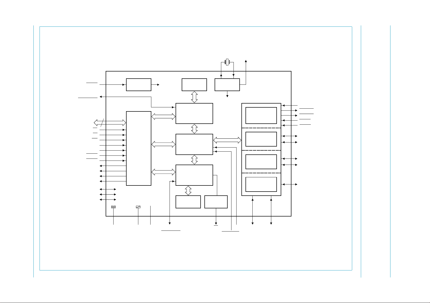
6. Block diagram
Philips Semiconductors
Single-chip USB OTG controller
Fig 1. Block diagram.
DGND AGND
V
CC
D_SUSPEND/
D_WAKEUP
GL
ID
OTGMODE
CP_CAP2 CP_CAP1
ISP1362
Philips Semiconductors
7. Pinning information
7.1 Pinning
ISP1362
Single-chip USB OTG controller
DGND
D2
D3
V
CC
D4
D5
D6
D7
DGND
D8
D9
D10
D11
V
CC
D12
D13
57
DD_5VVBUS
V
56
55
CP_CAP2
CP_CAP1
54
53
VCCAGND
52
51
OTG_DP1
OTG_DM1
50
49
48
ID
47
H_DP2
46
H_DM2
45
OTGMODE
44
X2
43
X1
42
H_OC1
41
H_OC2
40
V
CC
39
GL
38
CLKOUT
37
DGND
36
H_PSW2
35
H_PSW1
34
D_SUSPEND/D_WAKEUP
33
H_SUSPEND/H_WAKEUP
D1
D0
A1
A0
TEST2
TEST1
VCCDGND
64
63
62
61
60
59
58
1
2
3
4
5
6
7
8
9
10
11
12
13
14
15
16
ISP1362BD
17
18
19
20
21
22
23
24
25
26
27
28
29
30
31
32
004aaa050
CS
D14
D15
DGND
RD
WR
TEST0
DREQ1
DREQ2
CC
V
DGND
DACK1
DACK2
INT1
INT2
RESET
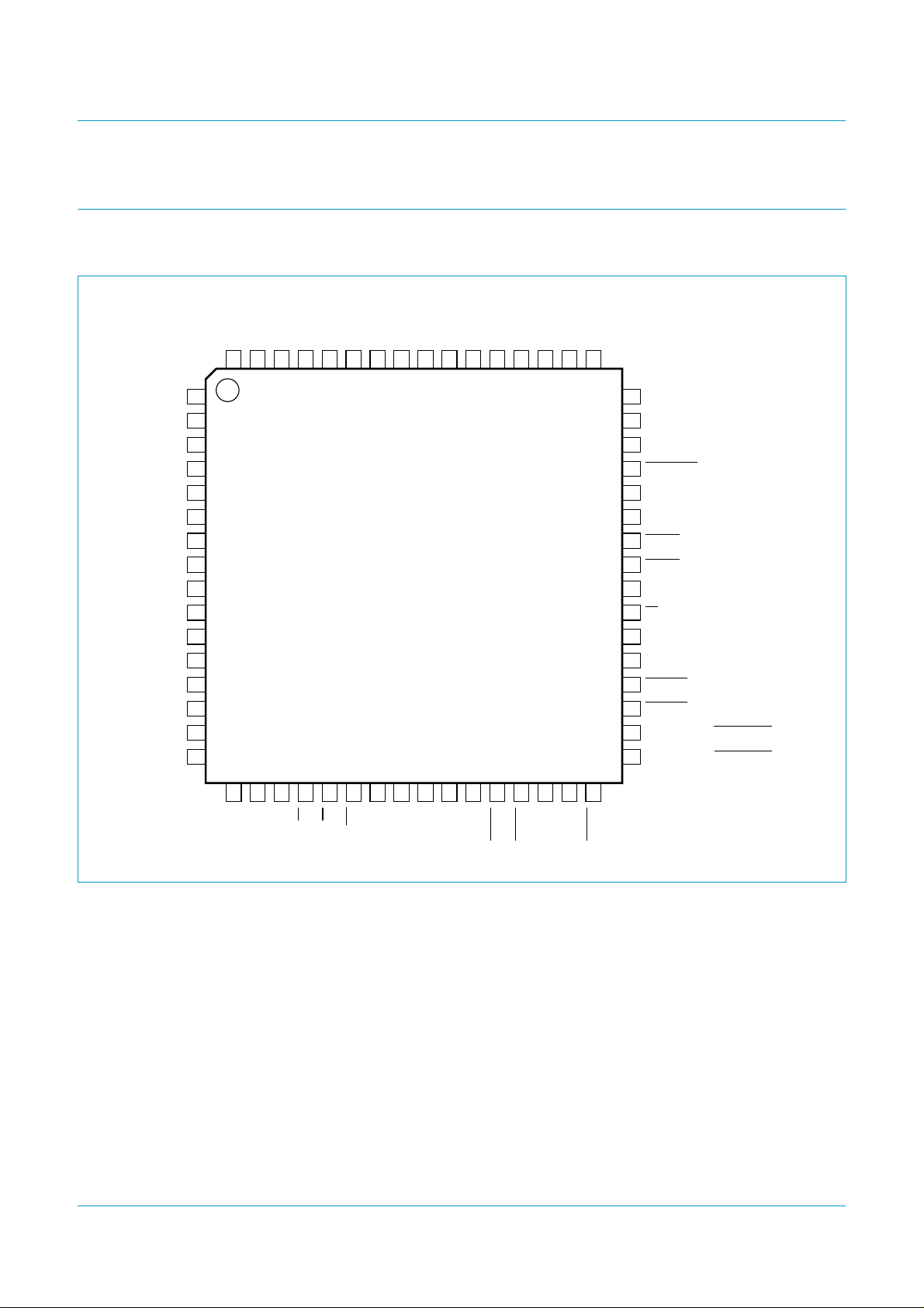
Fig 2. Pin configuration LQFP64.
9397 750 12337
Product data Rev. 03 — 06 January 2004 6 of 150
© Koninklijke Philips Electronics N.V. 2004. All rights reserved.
Philips Semiconductors
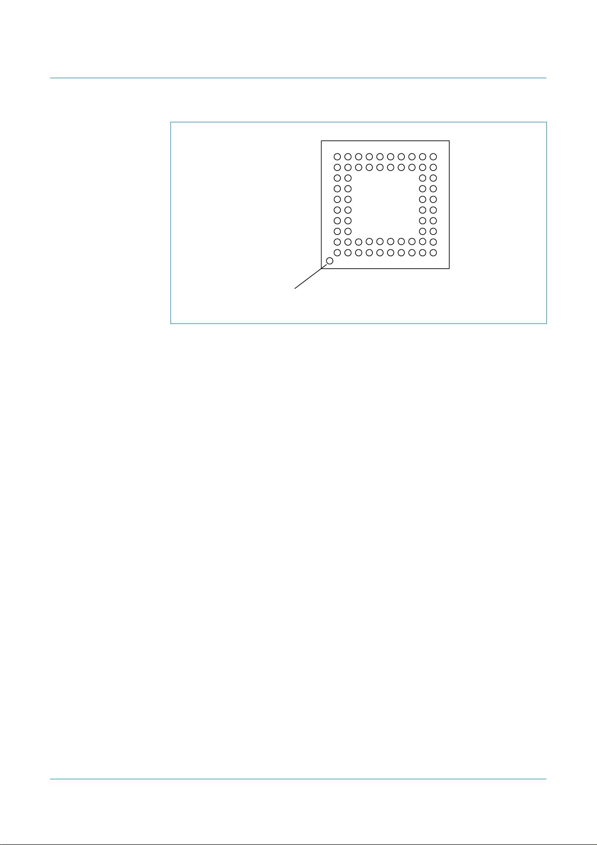
Fig 3. Pin configuration TFBGA64.
ball A1
index area
ISP1362
Single-chip USB OTG controller
004aaa151
K
J
H
G
F
E
D
C
B
A
ISP1362EE
ISP1362EE/01
24689101357
9397 750 12337
© Koninklijke Philips Electronics N.V. 2004. All rights reserved.
Product data Rev. 03 — 06 January 2004 7 of 150

Philips Semiconductors
ISP1362
Single-chip USB OTG controller
7.2 Pin description
Table 2: Pin description
CC
[1]
Pin
LQFP64
4 D2 - supply voltage (3.3 V); it is recommended to connect a decoupling
Ball
TFBGA64
Symbol
DGND 1 B1 - digital ground
D2 2 C2 I/O bit 2 ofthebidirectionaldata bus that connects to the internal registers
D3 3 C1 I/O bit 3 of the bidirectional data bus that connects to the internal registers
V
D4 5 D1 I/O bit 4 of the bidirectional data bus that connects to the internal registers
D5 6 E2 I/O bit 5 of the bidirectional data bus that connects to the internal registers
D6 7 E1 I/O bit 6 of the bidirectional data bus that connects to the internal registers
D7 8 F2 I/O bit 7 of the bidirectional data bus that connects to the internal registers
DGND 9 F1 - digital ground
D8 10 G2 I/O bit 8 of the bidirectional data bus that connects to the internal registers
D9 11 G1 I/O bit 9 of the bidirectional data bus that connects to the internal registers
D10 12 H2 I/O bit 10 of the bidirectional data bus that connects to the internal
D11 13 H1 I/O bit 11 of the bidirectional data bus that connects to the internal
Type
[2]
Description
and buffer memory of the ISP1362; the bus is in the high-impedance
state when it is idle
bidirectional, push-pull input, three-state output
and buffer memory of the ISP1362; the bus is in the high-impedance
state when it is idle
bidirectional, push-pull input, three-state output
capacitor of 0.01 µF
and buffer memory of the ISP1362; the bus is in the high-impedance
state when it is idle
bidirectional, push-pull input, three-state output
and buffer memory of the ISP1362; the bus is in the high-impedance
state when it is idle
bidirectional, push-pull input, three-state output
and buffer memory of the ISP1362; the bus is in the high-impedance
state when it is idle
bidirectional, push-pull input, three-state output
and buffer memory of the ISP1362; the bus is in the high-impedance
state when it is idle
bidirectional, push-pull input, three-state output
and buffer memory of the ISP1362; the bus is in the high-impedance
state when it is idle
bidirectional, push-pull input, three-state output
and buffer memory of the ISP1362; the bus is in the high-impedance
state when it is idle
bidirectional, push-pull input, three-state output
registers and buffer memory of the ISP1362; the bus is in the
high-impedance state when it is idle
bidirectional, push-pull input, three-state output
registers and buffer memory of the ISP1362; the bus is in the
high-impedance state when it is idle
bidirectional, push-pull input, three-state output
9397 750 12337
Product data Rev. 03 — 06 January 2004 8 of 150
© Koninklijke Philips Electronics N.V. 2004. All rights reserved.

Philips Semiconductors
ISP1362
Single-chip USB OTG controller
Pin
…continued
Ball
TFBGA64
Type
[2]
Description
Table 2: Pin description
Symbol
[1]
LQFP64
V
CC
14 J2 - supply voltage (3.3 V); it is recommended to connect a decoupling
capacitor of 0.01 µF
D12 15 J1 I/O bit 12 of the bidirectional data bus that connects to the internal
registers and buffer memory of the ISP1362; the bus is in the
high-impedance state when it is idle
bidirectional, push-pull input, three-state output
D13 16 K1 I/O bit 13 of the bidirectional data bus that connects to the internal
registers and buffer memory of the ISP1362; the bus is in the
high-impedance state when it is idle
bidirectional, push-pull input, three-state output
D14 17 K2 I/O bit 14 of the bidirectional data bus that connects to the internal
registers and buffer memory of the ISP1362; the bus is in the
high-impedance state when it is idle
bidirectional, push-pull input, three-state output
D15 18 J3 I/O bit 15 of the bidirectional data bus that connects to the internal
registers and buffer memory of the ISP1362; the bus is in the
high-impedance state when it is idle
bidirectional, push-pull input, three-state output
DGND 19 K3 - digital ground
RD 20 J4 I read strobe input; when asserted LOW, it indicates that the HC/DC
driver is requesting a read to the buffer memory or the internal
registers of the HC/DC
input with hysteresis
CS 21 K4 I chip select input (active LOW); enables the HC/DC driver to access
the buffer memory and registers of the HC/DC
input
WR 22 J5 I write strobe input; when asserted LOW, it indicates that the HC/DC
driver is requesting a write to the buffer memory or the internal
registers of the HC/DC
input with hysteresis
TEST0 23 K5 I/O for test input and output; pulled HIGH by a 100kΩ resistor
bidirectional, push-pull input, three-state output
DREQ1 24 J6 O DMA request output; when active, it signals the DMA controller that a
data transfer is requested by the HC; the active level (HIGH or LOW)
of the request is programmed by using the HcHardwareConfiguration
register (20H/A0H)
If the OneDMA bit of the HcHardwareConfiguration register is set to
logic 1, both the HC and DC DMA channel will be routed to DREQ1
DACK1.
and
push-pull output
DREQ2 25 K6 O DMA request output; when active, it signals the DMA controller that a
data transfer is requested by the DC; the active level (HIGH or LOW)
of the request is programmed by using the DcHardwareConfiguration
register (BAH/BBH)
push-pull output
9397 750 12337
Product data Rev. 03 — 06 January 2004 9 of 150
© Koninklijke Philips Electronics N.V. 2004. All rights reserved.

Philips Semiconductors
ISP1362
Single-chip USB OTG controller
Table 2: Pin description
Symbol
[1]
LQFP64
V
CC
26 J7 - supply voltage (3.3 V); it is recommended to connect a decoupling
Pin
…continued
Ball
TFBGA64
Type
[2]
Description
capacitor of 0.01 µF
DGND 27 K7 - digital ground
DACK1 28 J8 I DMA acknowledge input; indicates that a request for DMA transfer
from the HC has been granted by the DMA controller; the active level
(HIGH or LOW) of the acknowledgesignal is programmed byusing the
HcHardwareConfiguration register (20H/A0H); when not in use, this
pin must be connected to V
through a 10 kΩ resistor
CC
input with hysteresis
DACK2 29 K8 I DMA acknowledge input; indicates that a request for DMA transfer
from the DC has been granted by the DMA controller; the active level
(HIGH or LOW) of the acknowledgesignal is programmed byusing the
DcHardwareConfiguration register (BAH/BBH); when not in use, this
pin must be connected to V
through a 10 kΩ resistor
CC
input with hysteresis
INT1 30 J9 O interrupt request from the HC; provides a mechanism for the HC to
interrupt the microprocessor; see HcHardwareConfiguration register
(20H/A0H) Section 15.4.1 for details
If the OneINT bit of the HcHardwareConfiguration register is set to
logic 1, both the HC and DC interrupt request will be routed to INT1.
push-pull output
INT2 31 K9 O interrupt request from the DC; provides a mechanism for the DC to
interrupt the microprocessor; see DcHardwareConfiguration register
(BAH/BBH) Section 16.1.4 for details
push-pull output
RESET 32 K10 I reset input
input with hysteresis and internal pull-up resistor
H_SUSPEND/
H_WAKEUP
33 J10 I/O I/O pin (open-drain); goes HIGH when the HC is in the ‘suspend’
mode; a LOW pulse must be applied to this pin to wake up the HC;
connect a 100 kΩ resistor to V
CC
bidirectional, push-pull input, three-state open-drain output
D_SUSPEND/
D_WAKEUP
34 H9 I/O I/O pin (open-drain); goes HIGH when the DC is in the ‘suspend’
mode; a LOW pulse must be applied to this pin to wake up the DC;
connect a 100 kΩ resistor to V
CC
bidirectional, push-pull input, three-state open-drain output
H_PSW1 35 H10 O connects to the external PMOS switch; required when the external
charge pump or external V
is used for providing V
BUS
BUS
to the
downstream port
LOW — switches ON the PMOS providing V
to the downstream
BUS
port
HIGH — switches OFF the PMOS
when not in use, leave this pin open
open-drain output
9397 750 12337
Product data Rev. 03 — 06 January 2004 10 of 150
© Koninklijke Philips Electronics N.V. 2004. All rights reserved.

Philips Semiconductors
Single-chip USB OTG controller
Table 2: Pin description…continued
Symbol
[1]
Pin
LQFP64
Ball
TFBGA64
H_PSW2 36 G9 O connects to the external PMOS switch
Type
[2]
Description
ISP1362
LOW — switches ON the PMOS providing V
to the downstream
BUS
port
HIGH — switches OFF the PMOS
when not in use, leave this pin open
open-drain output
DGND 37 G10 - digital ground
CLKOUT 38 F9 O programmable clock output; the default clock frequency is 12 MHz and
can be varied from 3 MHz to 48 MHz
push-pull output
GL 39 F10 O GoodLink LED indicator output; the LED is OFF by default, blinks ON
upon USB traffic
open-drain output; 4 mA
V
CC
40 E9 - supply voltage (3.3 V); it is recommended to connect a decoupling
capacitor of 0.01 µF
H_OC2 41 E10 I overcurrent sense input for downstream port 2; both the digital and
analog overcurrent inputs can be used for port 2, depending on the
hardware mode register setting; when not in use, it is recommended to
connect this pin to the V
DD_5V
pin
H_OC1 42 D9 I overcurrent sensing input for downstream port 1; both the digital and
analog overcurrent inputs can be used for port 1, depending on the
hardware mode register setting; when not in use, it is recommended to
connect this pin to the V
DD_5V
pin
X1 43 D10 AI crystal input; connected directly to a 12 MHz crystal; when this pin is
connected to an external clock oscillator, leave pin X2 open
X2 44 C9 AO crystal output; connected directly to a 12 MHz crystal; when pin X1 is
connected to an external clock oscillator, leave this pin open
OTGMODE 45 C10 I to select whether port 1 is operating in the OTG or non-OTG mode;
see Table 8
input with hysteresis
H_DM2 46 B9 AI/O downstream D− signal; host only, port 2; when not in use, leave this
pin open and set bit ConnectPullDown_DS2 of the
HcHardwareConfiguration register
H_DP2 47 B10 AI/O downstream D+ signal; host only, port 2; when not in use, leave this
pin open and set bit ConnectPullDown_DS2 of the
HcHardwareConfiguration register
ID 48 A10 I input pin for sensing OTG ID; the status of this input pin is reflected in
the OTGStatus register (bit 0); see Table 8
input with hysteresis
OTG_DM1 49 A9 AI/O D− signal of the OTG port, the downstream host port 1 or the
upstream device port; when not in use, leave this pin open and set
bit ConnectPullDown_DS1 of the HcHardwareConfiguration register
OTG_DP1 50 B8 AI/O D+ signal of the OTG port, the downstream host port 1 or the
upstream device port; when not in use, leave this pin open and set
bit ConnectPullDown_DS1 of the HcHardwareConfiguration register
[3]
[3]
9397 750 12337
Product data Rev. 03 — 06 January 2004 11 of 150
© Koninklijke Philips Electronics N.V. 2004. All rights reserved.

Philips Semiconductors
ISP1362
Single-chip USB OTG controller
Pin
…continued
Ball
TFBGA64
Type
[2]
Description
Table 2: Pin description
Symbol
[1]
LQFP64
AGND 51 A8 - analog ground; used for OTG ATX
V
CC
52 B7 - supply voltage (3.3 V); it is recommended to connect a decoupling
capacitor of 0.01 µF
CP_CAP1 53 A7 AI/O charge pump capacitor pin 1; low ESR; see Section 11.6
CP_CAP2 54 B6 AI/O charge pump capacitor pin 2; low ESR; see Section 11.6
V
BUS
55 A6 I/O analog input and output
OTG mode — built-in charge pump output or V
comparators input; connect to pin V
DC mode — input as V
of the OTG connector
BUS
sensing; connect to pin V
BUS
BUS
voltage
BUS
of the
upstream connector
HC mode — not used; leave open
V
DD_5V
56 B5 I supply reference voltage (5 V); to be used together with built-in
overcurrent circuit; when built-in overcurrent circuit is not in use, this
pin can be tied to V
; it is recommended to connect a decoupling
CC
capacitor of 0.01 µF
DGND 57 A5 - digital ground
V
CC
58 B4 - supply voltage (3.3 V); it is recommended to connect a decoupling
capacitor of 0.01 µF
TEST1 59 A4 I/O for test input and output, pulled to GND by a 10 kΩ resistor
bidirectional, push-pull input, three-state output
TEST2 60 B3 I/O for test input and output, pulled to GND by a 10 kΩ resistor
bidirectional, push-pull input, three-state output
A0 61 A3 I command or data phase
input
A1 62 B2 I LOW — PIO bus of the HC is selected
HIGH — PIO bus of the DC is selected
input
D0 63 A2 I/O bit 0 of the bidirectional data bus that connects to the internal registers
and buffer memory of the ISP1362; the bus is in the high-impedance
state when it is idle
bidirectional, push-pull input, three-state output
D1 64 A1 I/O bit 1 of the bidirectional data bus that connects to the internal registers
and buffer memory of the ISP1362; the bus is in the high-impedance
state when it is idle
bidirectional, push-pull input, three-state output
[1] Symbol names with an overscore (for example, NAME) represent active LOW signals.
[2] All I/O pads are 5 V tolerant.
[3] In the OTG mode, this pin is pulled down by an internal resistor.
9397 750 12337
Product data Rev. 03 — 06 January 2004 12 of 150
© Koninklijke Philips Electronics N.V. 2004. All rights reserved.

Philips Semiconductors
8. Functional description
8.1 On-The-Go (OTG) controller
The OTG Controller provides all the control, monitoring and switching functions
required in OTG operations.
8.2 Advanced Philips Slave Host Controller (PSHC)
The advanced Philips Slave HC is designed for highly optimized USB host
functionality. Many advanced features are integrated to fully utilize the USB
bandwidth. A number of tasks are performed at the hardware level. This reduces the
requirement on the microprocessor and thus speeds up the system.
8.3 Philips Device Controller (DC)
The Philips DC is a high performance USB device with up to 14 programmable
endpoints. These endpoints can be configured as double-buffered endpoints to
further enhance the throughput.
ISP1362
Single-chip USB OTG controller
8.4 Phase-Locked Loop (PLL) clock multiplier
A 12 MHz-to-48 MHz clock multiplier PLL is integrated on-chip. This allows the use of
a low-cost 12 MHz crystal that also minimizes Electro-Magnetic Interference (EMI)
because of low frequency. No external components are required for the operation of
PLL.
8.5 USB and OTG transceivers
The integrated transceivers (for typical downstream port) directly interface to the USB
connectors (type A) and cables through some termination resistors. The transceiver
is compliant with Universal Serial Bus Specification Rev 2.0.
8.6 Overcurrent protection
The ISP1362 has a built-in overcurrent protection circuitry. This feature monitors the
current drawn on the downstream V
exceedsthe current threshold. The built-in overcurrent protection feature can be used
when the port acts as a host port.
and switches off V
BUS
when the current
BUS
8.7 Bus interface
The bus interface connects the microprocessor to the USB host and the USB device
allowing fast and easy access to both.
8.8 DC and HC buffer memory
4096 bytes (host) and 2462 bytes (device)of built-in memory provide sufficient space
forthe buffering of USB traffic. Memory in the HC is addressable by using the fast and
versatile direct addressing method.
9397 750 12337
Product data Rev. 03 — 06 January 2004 13 of 150
© Koninklijke Philips Electronics N.V. 2004. All rights reserved.

Philips Semiconductors
8.9 GoodLink
Indication of a good USB connection is provided through the GoodLink technology
(open-drain, maximum current: 4 mA). During enumeration, LED indicators blink ON
momentarily corresponding to the enumeration traffic of the ISP1362 ports. The LED
also blinks ON whenever there is valid traffic to the USB ports. In the ‘suspend’ mode,
the LED is OFF.
This feature of GoodLink provides a user-friendly indication on the status of the USB
traffic between the host and the hub, as well as the connected devices. It is a useful
diagnostics tool to isolate faulty equipment and helps to reduce field support and
hotline costs.
8.10 Charge pump
ISP1362
Single-chip USB OTG controller
The charge pump generates a 5 V supply from 3.3 V to drive V
is an A-device in the OTG mode. For details, see Section 11.6.
9. Host and device bus interface
The interface between the external microprocessor and the ISP1362 Host Controller
(HC) and Device Controller (DC) is separately handled by the individual bus interface
circuitry. The host or device automux selects the path for the host access or the
device access. This selection is determined by the A1 address line. For any access
to HC or DC registers, the command phase and the data phase are needed, which is
determined by the A0 address line.
All the functionality of the ISP1362 can be accessed using a group of registers and
two buffer memory areas (one for the HC and the other the DC). Registers can be
accessed using the Programmed I/O (PIO) mode. The buffer memory can be
accessed using both the PIO and direct memory access (DMA) modes.
When CS is LOW (active), the address pin A1 has priority over DREQ and DACK.
Therefore, as long as the CS pin is held LOW, the ISP1362 bus interface does not
respond to any DACK signals. When CS is HIGH (inactive), the bus interface will
respond to DREQn and DACKn. The address pin A1 will be ignored when CS is
inactive.
An active DACKn signal when the DREQn is inactive will be ignored. If DREQ1,
DACK1, DREQ2 and DACK2 are active, the bus interface will be switched off to avoid
potential data corruption.
when the ISP1362
BUS
Table 3 provides the bus access priority for the ISP1362.
Table 3: Bus access priority table for the ISP1362
Priority CS A1 DACK1 DACK2 DREQ1 DREQ2 HC and DC active
1LLXXXXHC
2LHXXXXDC
3HXLXHLHC
4HXXLLHDC
5 H X X X H H no driving
[1] Only for enabling of the bus and disabling of the bus. Depends only on the DACK signal.
9397 750 12337
Product data Rev. 03 — 06 January 2004 14 of 150
© Koninklijke Philips Electronics N.V. 2004. All rights reserved.
[1]
[1]

Philips Semiconductors
9.1 Memory organization
The buffer memory in the HC uses a multiconfigurable direct addressing architecture.
The 4096 bytes HC buffer memory is shared by the ISTL0, ISTL1, INTL and ATL
buffers. ISTL0 and ISTL1 are used for isochronous traffic (double buffer), INTL is
used for interrupt traffic, and ATL is used for control and bulk traffic.
The allocation of the buffer memory follows the sequence ISTL0, ISTL1, INTL, ATL
and unused memory. For example, consider that the buffer sizes of the ISTL, INTL
and ATL buffers are 1024 bytes, 1024 bytes and 1024 bytes, respectively. Then,
ISTL0 will start from memory location 0, ISTL1 will start from memory location 1024
(size of ISTL0), INTL will start from memory location 2048 (size of ISTL0 + size of
ISTL1) and ATL will start from memory location 3072 (size of ISTL0 + size of
ISTL1 + size of INTL).
The HCD has the responsibility to ensure that the sum of the four memory buffers
does not exceed the total memory size. If this condition is violated, it will lead to data
corruption. The buffer size must be a multiple of two bytes (one word).
The buffer memory of the DC follows a similar architecture. Details on the DC
memory area allocation can be found in Section 13.3. Note that the DC buffer
memory does not support the direct addressing mode.
ISP1362
Single-chip USB OTG controller
9.1.1 Memory organization for the HC
The HC in the ISP1362 has a total of 4096 bytes of buffer memory. This buffer area is
divided into four parts (see Table 4 and Figure 4):
Table 4: Buffer memory areas and their applications
Buffer memory area Application
ISTL0 and ISTL1 isochronous transfer (double buffering)
INTL interrupt transfer
ATL control and bulk transfer
The ISTL0 and ISTL1 buffers must have the same size. Memory is allocated by
the HC according to the value set by the HCD in HcISTLBufferSize,
HcINTLBufferSize and HcATLBufferSize. All buffer sizes must be multiples of two
bytes (one word).
9397 750 12337
Product data Rev. 03 — 06 January 2004 15 of 150
© Koninklijke Philips Electronics N.V. 2004. All rights reserved.

Philips Semiconductors
0x0000
0x03FF
0x0400
0x07FF
0x0800
0x09FF
0x0A00
ISP1362
Single-chip USB OTG controller
ISTL0 area (512 bytes)
ISTL1 area (512 bytes)
INTL area (512 bytes)
ATL area (1536 bytes)
0x0FFF
004aaa053
Fig 4. Recommended values of the ISP1362 buffer memory allocation.
The INTL and ATL buffers use ‘blocked memory management’ scheme to enhance
the status and control capability of each and every individual PTD structure. The INTL
and ATL buffers are further divided into blocks of equal sizes depending on the value
written to the HcATLBlkSize register (ATL) and the HcINTLBlkSize register (INTL).
The ISP1362 HC supports up to 32 blocks in the ATL and INTL buffers. Each of these
blocks can be used for one complete Philips Transfer Descriptor (PTD) data.
Note that the block size does not include the 8-byte PTD header and is strictly the
size of the payload. Both the ATL and INTL block sizes must be a multiple of DWord
(4 bytes).
9397 750 12337
Product data Rev. 03 — 06 January 2004 16 of 150
© Koninklijke Philips Electronics N.V. 2004. All rights reserved.
Philips Semiconductors
Starting address of the
ATL or INTL buffer area
ISP1362
Single-chip USB OTG controller
8 bytes PTD header
64 bytes PTD header
Payload area
8 bytes PTD header
64 bytes PTD header
Payload area
8 bytes PTD header
64 bytes PTD header
Payload area
004aaa055
Block of 72 bytes
(64 + 8,
where 64 is the block size defined)
72 bytes
72 bytes
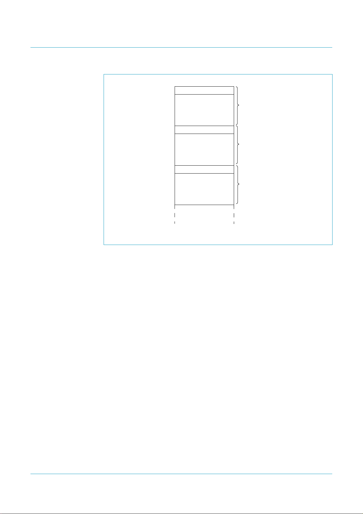
Fig 5. A sample snapshot of the ATL or INTL memory management scheme.
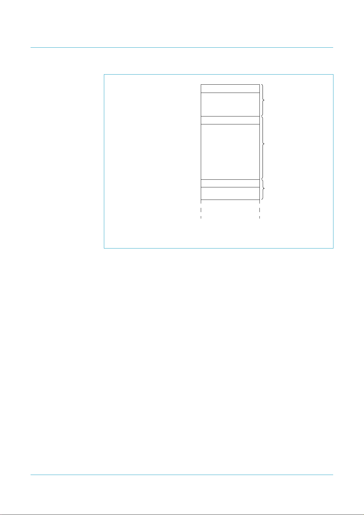
Figure 5 provides a snapshot of a sample ATL or INTL buffer area of 256 bytes with a
block size of 64 bytes. The HCD may put a PTD with payload size of up to 64 bytes
but not more. Depending on the ATL or INTL buffer size, up to 32 ATL blocks and
32 INTL blocks can be allocated. Note that a portion of the ATL or INTL buffer
remains unused. This is allowed but can be avoided by choosing the appropriate ATL
or INTL buffer size and block size.
The ISTL0 or ISTL1 buffer memory (for isochronous transfer) uses a different
memory management scheme (see Figure 6). There is no fixed block size for the
ISTL buffer memory. While the PTD header remains 8 bytes for all PTDs, the PTD
payload can be of any size. The PTD payload, however, is padded to the next DWord
boundary when the HC calculates the location of the next PTD header. The
ISP1362 HC checks the payload size from the ‘Total size’ field of the PTD itself and
calculates the location of the next PTD header based on this information.
9397 750 12337
Product data Rev. 03 — 06 January 2004 17 of 150
© Koninklijke Philips Electronics N.V. 2004. All rights reserved.
Philips Semiconductors
ISP1362
Single-chip USB OTG controller
Starting address of ISTL0 or ISTL1
‘Total size’ is a 10-bit field in the PTD.
Fig 6. A sample snapshot of the ISTL memory management scheme.
9.1.2 Memory organization for the DC
The ISP1362 DC has a total of 2462 bytes of built-in buffer memory. This buffer
memory is multiconfigurable to support the requirements of differentapplications. The
DC buffer memory is divided into 16 areas to be used by control OUT, control IN and
14 programmable endpoints.
PTD header (Total size = 64)
PTD payload (64 bytes)
PTD header (Total size = 160)
PTD payload (160 bytes)
PTD header (Total size = 32)
PTD payload (32 bytes)
004aaa054
72 bytes (64 + 8)
168 bytes (160 + 8)
40 bytes (32 + 8)
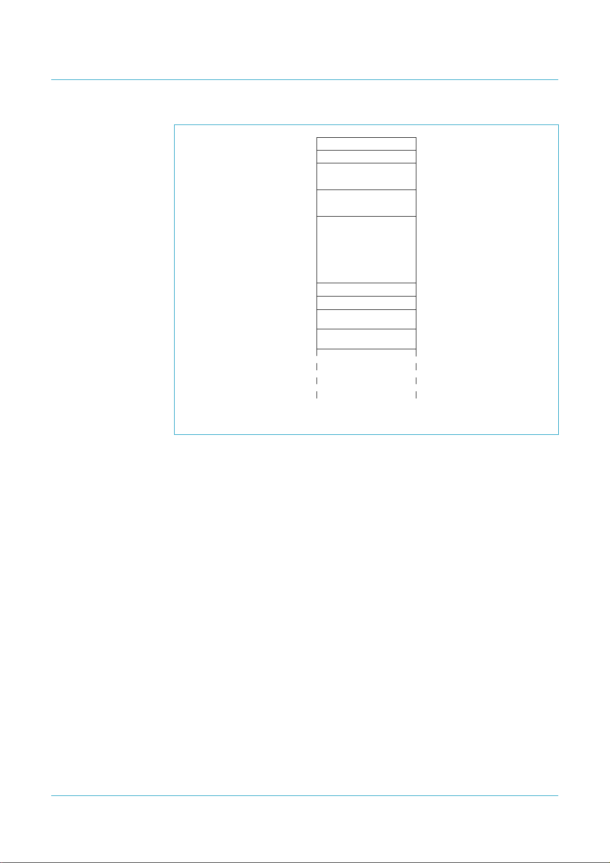
Figure 7 provides a snapshot of the DC buffer memory.
9397 750 12337
Product data Rev. 03 — 06 January 2004 18 of 150
© Koninklijke Philips Electronics N.V. 2004. All rights reserved.
Philips Semiconductors
ISP1362
Single-chip USB OTG controller
Control OUT (64 bytes)
Control IN (64 bytes)
Endpoint 1 (128 bytes)
Endpoint 2 (128 bytes)
Endpoint 3 (512 bytes)
Endpoint 4 (64 bytes)
Endpoint 5 (64 bytes)
Endpoint 6 (96 bytes)
Endpoint 7 (96 bytes)
004aaa057
Fig 7. DC buffer memory organization.
The buffer memory is configured by the DcEndpointConfiguration registers (ECRs).
Although the control endpoint has a fixedconfiguration, all 16 endpoints (control OUT,
control IN and 14 programmable endpoints) must be configured before the DC
internally allocates the buffer.The 14 programmable endpoints could be programmed
into sizes ranging from 16 bytes to 1023 bytes, single or double buffering.
The DC buffer memory for each endpoint can be accessed through the
DcReadEndpointBuffer and DcWriteEndpointBuffer registers.
9.2 PIO access mode
The ISP1362 provides the PIO mode for external microprocessors to access its
internal control registers and buffer memory. It occupies only four I/O ports or four
memory locations of a microprocessor. An external microprocessor can read or write
to the internal control registers and buffer memory of the ISP1362 through the PIO
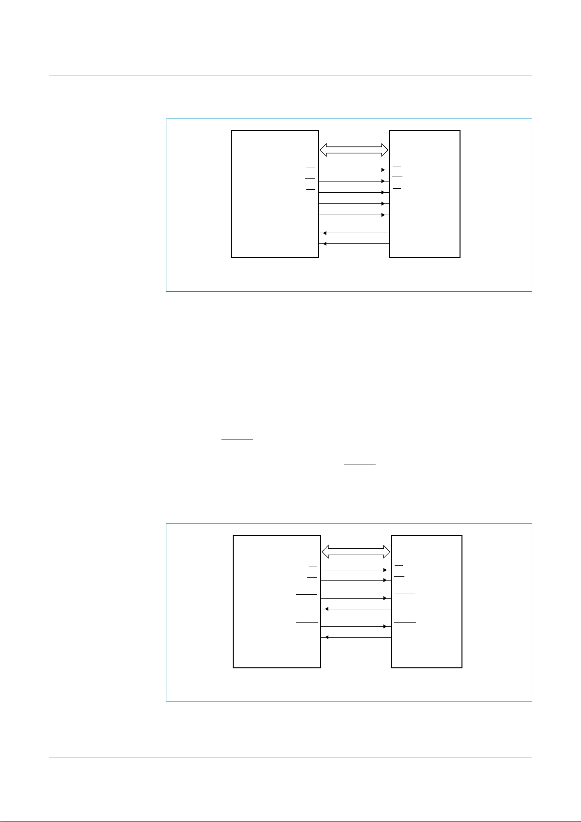
operating mode. Figure 8 shows the PIO interface between a microprocessor and the
ISP1362.
9397 750 12337
Product data Rev. 03 — 06 January 2004 19 of 150
© Koninklijke Philips Electronics N.V. 2004. All rights reserved.
Philips Semiconductors
ISP1362
Single-chip USB OTG controller
MICRO-
PROCESSOR
D[15:0
WR
IRQ1
IRQ2
µP bus interface
]
RD
CS
A2
A1
D[15:0
RD
WR
CS
A1
A0
INT1
INT2
]
ISP1362
004aaa042
Fig 8. PIO interface between a microprocessor and the ISP1362.
9.3 DMA mode
The ISP1362 also provides the DMA mode for external microprocessors to access
the internal buffer memory of the ISP1362. The DMA operation enables data to be
transferred between the system memory of a microprocessor and the internal buffer
memory of the ISP1362.
Remark: The DMA operation must be controlled by the DMA controller of the external
microprocessor system (master). Figure 9 shows the DMA interface between a
microprocessor system and the ISP1362.
The ISP1362 provides two DMA channels. The DMA channel 1 (controlled by the
DREQ1 and DACK1 signals) is for the DMA transfer between the system memory of
a microprocessor and the internal buffer memory of the ISP1362 HC. The DMA
channel 2 (controlled by the DREQ2 and DACK2 signals) is for the DMA transfer
between the system memory of a microprocessor and the internal buffer memory of
the ISP1362 DC. The ISP1362 provides an internal End-Of-Transfer (EOT) signal to
terminate the DMA transfer.
µP bus interface
]
D[15:0
RD
WR
MICRO-
PROCESSOR
DACK1
DREQ1
DACK2
DREQ2
Fig 9. DMA interface between a microprocessor and the ISP1362.
D[15:0
RD
WR
DACK1
DREQ1
DACK2
DREQ2
]
ISP1362
004aaa043
9397 750 12337
© Koninklijke Philips Electronics N.V. 2004. All rights reserved.
Product data Rev. 03 — 06 January 2004 20 of 150
Philips Semiconductors
9.4 PIO access to internal control registers
Table 5 shows the I/O port addressing in the ISP1362. The complete I/O port address
decoding should combine with the chip select signal (CS) and the address lines (A1
and A0). The direction of access of I/O ports, however, is controlled by the RD and
WR signals
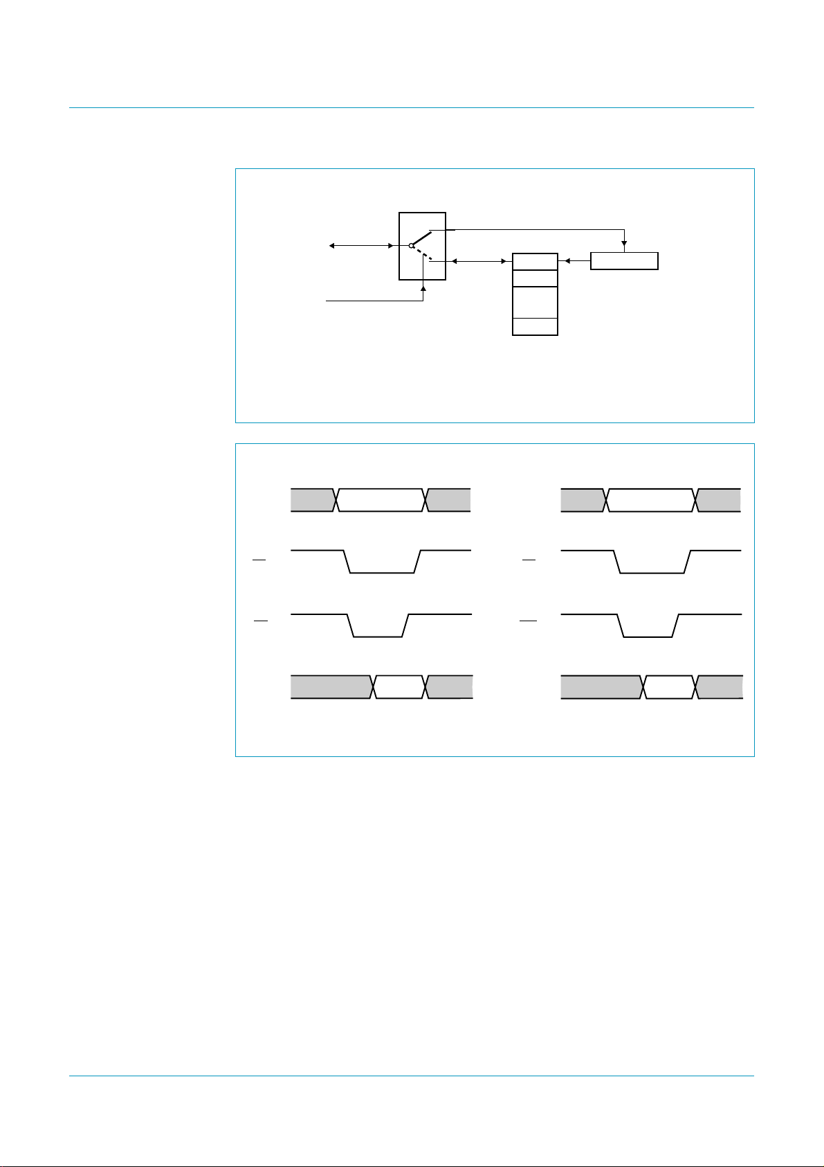
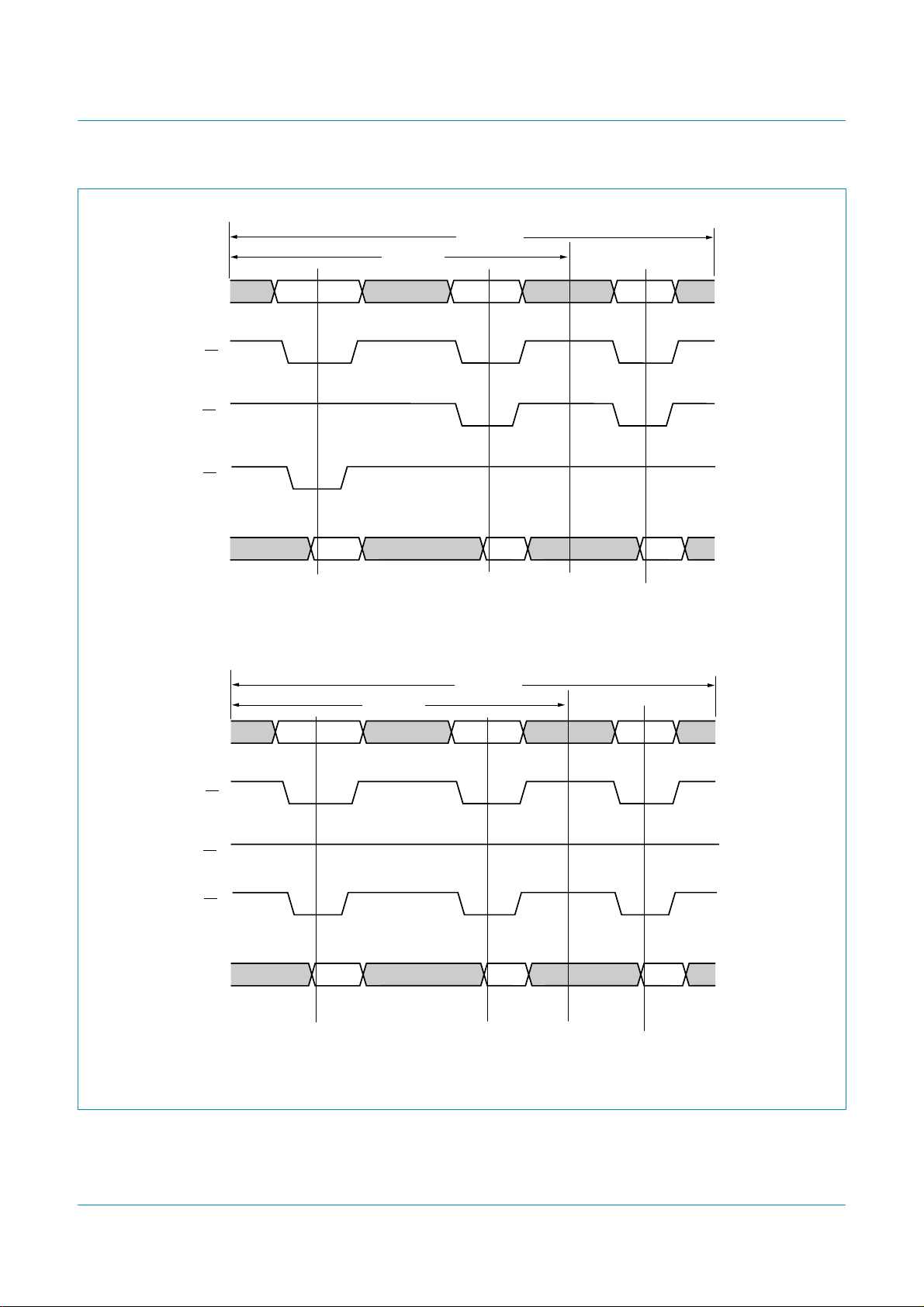
When RD is LOW, the microprocessor reads data from the data port of the ISP1362
(see Figure 10). When WR is LOW, the microprocessor writes command to the
command port or writes data to the data port (see Figure 11).
Table 5: I/O port addressing
CS A1 A0 Access Data bus width Description
L L L R/W 16 bits HC data port
L L H W 16 bits HC command port
L H L R/W 16 bits DC data port
L H H W 16 bits DC command port
The register structure in the ISP1362 is a command-data register pair structure. A
complete register access needs a command phase followed by a data phase. The
command (also named as the index of a register) is used to inform the ISP1362 about
the register that will be accessed at the data phase.
ISP1362
Single-chip USB OTG controller
On the 16-bit data bus of a microprocessor, a command occupies the lower byte and
the upper byte is filled with zeros (see Figure 12).
For 32-bit registers, the access cycle is shown in Figure 13. It consists of a command
phase followed by two data phases.
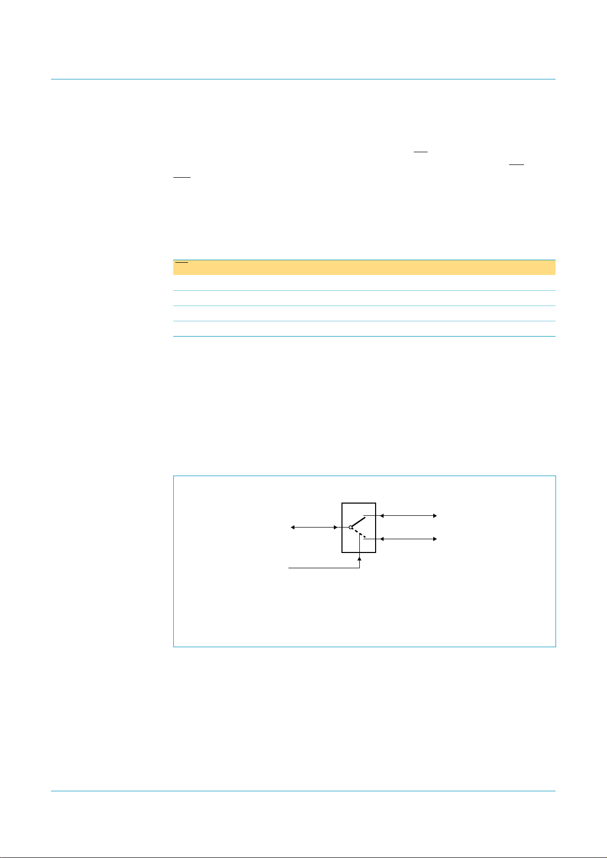
BUS INTERFACE
Host bus interface
µP bus interface
A1
When A1 = L, microprocessor accesses the HC.
When A1 = H, microprocessor accesses the DC.
Fig 10. Microprocessor access to the HC or the DC.
0
Device bus interface
1
004aaa122
9397 750 12337
Product data Rev. 03 — 06 January 2004 21 of 150
© Koninklijke Philips Electronics N.V. 2004. All rights reserved.
Philips Semiconductors
Host or Device
bus interface
A0
CMD/DATA
SWITCH
1
0
command port
data port
ISP1362
Single-chip USB OTG controller
Commands
Command register
.
.
.
When A0 = L, microprocessor accesses the data port.
When A0 = H, microprocessor accesses the command port.
Fig 11. Access to internal control registers.
Read 16-bit
A0/A1
CS
RD
D[15:0]
Control registers
A0/A1
CS
WR
D[15:0]
004aaa160
Write16-bit
004aaa045
Fig 12. PIO register access.
9397 750 12337
Product data Rev. 03 — 06 January 2004 22 of 150
© Koninklijke Philips Electronics N.V. 2004. All rights reserved.
Philips Semiconductors
A0/A1
CS
RD
WR
D[15:0]
ISP1362
Single-chip USB OTG controller
Reading from a 16/32-bit register
32-bit access
16-bit access
A0/A1
RD
WR
D[15:0]
CS
Command phase
16-bit access
Data phase
Writing to a 16/32-bit register
32-bit access
Second data phase
for 32-bit register
Command phase
Data phase
Second data phase
for 32-bit register
004aaa046
Fig 13. PIO access for a 16 or 32-bit register.
9397 750 12337
Product data Rev. 03 — 06 January 2004 23 of 150
© Koninklijke Philips Electronics N.V. 2004. All rights reserved.

Philips Semiconductors
The following is a sample code for PIO access to internal control registers:
unsigned long read_reg32(unsigned char reg_no)
{
unsigned int result_l,result_h;
unsigned long result;
outport(hc_com, reg_no); // Command phase
result_l=inport(hc_data); // Data phase
result_h=inport(hc_data); // Data phase
result = result_h;
result = result<<16;
result = result+result_l;
return(result);
}
void write_reg32(unsigned char reg_no, unsigned long data2write)
{
unsigned int low_word;
unsigned int hi_word;
ISP1362
Single-chip USB OTG controller
low_word=data2write&0x0000FFFF;
hi_word=(data2write&0xFFFF0000)>>16;
outport(hc_com,reg_no|0x80); // Command phase
outport(hc_data,low_word); // Data phase
outport(hc_data,hi_word); // Data phase
}
unsigned int read_reg16(unsigned char reg_no)
{
unsigned int result;
outport(hc_com, reg_no); // Command phase
result=inport(hc_data); // Data phase
return(result);
}
void write_reg16(unsigned char reg_no, unsigned int data2write)
{
outport(hc_com,reg_no|0x80); // Command phase
outport(hc_data,data2write); // Data phase
}
9.5 PIO access to the buffer memory
The buffer memory in the ISP1362 can be addressed using either the direct
addressing method or the indirect addressing method.
9.5.1 PIO access to the buffer memory by using direct addressing
This method uses the HcDirectAddressLength register to specify two parameters
required to randomly access the ISP1362 buffer memory (total of 4096 bytes). These
two parameters are:
9397 750 12337
Product data Rev. 03 — 06 January 2004 24 of 150
© Koninklijke Philips Electronics N.V. 2004. All rights reserved.

Philips Semiconductors
Starting address — Location to start writing or reading
Data length — Number of bytes to write or read.
The following is a sample code for setting the HcDirectAddressLength register:
void Set_DirAddrLen(unsigned int data_length,unsigned int addr)
{
unsigned long RegData = 0;
RegData =(long)(addr&0x7FFF);
RegData|=(((long)data_length)<<16);
write_reg32(HcDirAddrLen,RegData);
}
After the proper value is written to the HcDirectAddressLength register, data is
accessible from the HcDirectAddressData register (called as HcDirAddr_Port in the
following sample code). A sample code for writing word_size bytes of data from
*w_ptr to the memory locations of the ISP1362 buffer starting from the address
start_addr is as follows:
ISP1362
Single-chip USB OTG controller
void direct_write(unsigned int *w_ptr,unsigned int
start_addr,unsigned int word_size)
{
unsigned int cnt=0;
Set_DirAddrLen(word_size*2,start_addr);
outport(hc_com,HcDirAddr_Port|0x80); // hc_com is system address of
// HC command port
do
{
outport(hc_data,*(w_ptr+cnt)); // hc_data is system address of
// HC data port
cnt++;
}
while(cnt<word_size);
}
Direct addressing allows fast and random access to any location within the ISP1362
memory. Your program, however, needs the address location of each buffer area to
access them.
9.5.2 PIO access to the buffer memory by using indirect addressing
Indirect addressing is the addressing method that is compatible with the Philips
ISP1161 addressing mode. This method uses a unique data port for each buffer
memory area (ATL, INTL, ISTL0 and ISTL1). These four data areas share the
HcTransferCounter register that is used to indicate the number of bytes to be
transferred.
A sample code for writing an array at *a_ptr into the ATLmemory area with word_size
as the word size is given as follows:
void write_atl(unsigned int *a_ptr, unsigned int word_size)
{
int cnt;
9397 750 12337
Product data Rev. 03 — 06 January 2004 25 of 150
© Koninklijke Philips Electronics N.V. 2004. All rights reserved.

Philips Semiconductors
write_reg16(HcTransferCnt,word_size*2);
outport(hc_com,HcATL_Port|0x80); // hc_com is system address of HC
cnt=0;
do
{
outport(hc_data,*(a_ptr+cnt)); // hc_data is system address of HC
cnt++;
}
while(cnt<(word_size));
Remark: The HcTransferCounter register counts the number of bytes even though
the transfer is in number of words. Therefore, the transfer counter should be set to
word_size × 2. Incorrect setting of the HcTransferCounter register may cause the
ISP1362 to go into an indeterminate state.
The buffermemory access using indirect addressing always starts from the location 0
of each buffer area. Only the front portion of the memory (example: first 64 bytes of a
1024 bytes buffer) can be accessed. Therefore, to access a portion of the memory
that does not start from memory location 0, all memory locations before that location
must be accessed in a sequential order. The method is similar to the sequential file
access method.
ISP1362
Single-chip USB OTG controller
// command port
// data port
9.6 Setting up a DMA transfer
The ISP1362 uses two DMA channels to individually serve the HC and the DC. The
DMA transfer allows the system CPU to work on other tasks while the DMA controller
transfers data to or from the ISP1362. The DMA slave controller, in the ISP1362, is
compatible with the 8327 type DMA controller.
The DMA transfer can be used with the direct addressing mode or the indirect
addressing mode. The registers used in these two modes are shown in Table 6.
Table 6: Registers used in addressing modes
Addressing mode
Direct addressing 1XXB HcDirectAddressLength
Indirect addressing 0XXB HcTransferCounter
[1] In the direct addressing mode, HcTransferCounter must be set to 0001H.
[1]
HcDMAConfiguration bit[3:1] Total bytes to transfer
9.6.1 Configuring registers for a DMA transfer
To set up a DMA transfer, the following HC registers must be configured depending
on the type of transfer required:
• HcHardwareConfiguration
– DREQ1 output polarity (bit 5)
– DACK1 input polarity (bit 6)
– DACK mode (bit 8).
• HcµPInterruptEnable
– If you want an interrupt to be generated after the DMA transfer is complete, set
EOTInterruptEnable (bit 3).
9397 750 12337
Product data Rev. 03 — 06 January 2004 26 of 150
© Koninklijke Philips Electronics N.V. 2004. All rights reserved.

Philips Semiconductors
• HcµPInterrupt
• HcTransferCounter
• HcDMAConfiguration
Remark: Configure the HcDMAConfiguration register only after you have configured
all the other registers. The ISP1362 will assert DREQ1 once the DMA enable bit in
this register is set.
ISP1362
Single-chip USB OTG controller
– Before initiating the DMA transfer, clear AllEOTInterrupt (bit 3). This bit is set
when the DMA transfer is complete.
– If DMACounterEnable of the HcDMAConfiguration register is set (that is, the
DMA counter is enabled), HcTransferCounter must be set to the number of
bytes to be transferred.
– Read or write DMA (bit 0)
– Targeted buffer:ISTL0, ISTL1, ATL and INTL (bits 1 to 3)
– DMA enable or disable (bit 4)
– Burst length (bits 5 to 6)
– DMA counter enable (bit 7).
9.6.2 Combining the two DMA channels
The ISP1362 allows systems with limited DMA channels to use a single DMA channel
(DMA1) for both the HC and the DC. This option can be enabled by writing logic 1 to
the OneDMA bit of the HcHardwareConfiguration register. If this option is enabled,
the polarity of the DC DMA and the HC DMA must be set to DACK active LOW and
DREQ active HIGH.
9.7 Interrupts
Various events in the HC, the DC and the OTG controller can be programmed to
generate a hardware interrupt. By default, the interrupt generated by the HC and the
OTG controller is routed out at the INT1 pin and the interrupt generated by the DC is
routed out at the INT2 pin.
9.7.1 Interrupt in the HC and the OTG controller
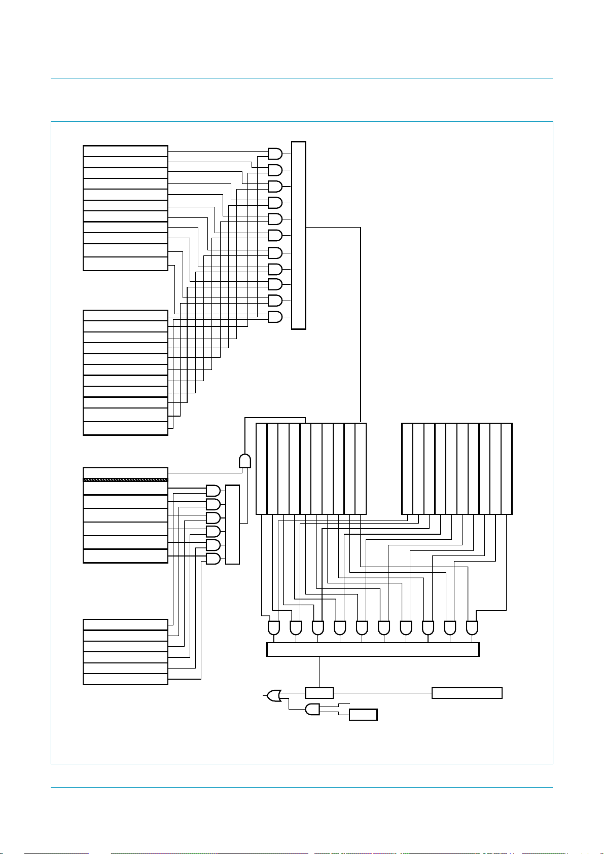
There are two levels of interrupts represented by level 1 and level 2 (see Figure 14).
9397 750 12337
Product data Rev. 03 — 06 January 2004 27 of 150
© Koninklijke Philips Electronics N.V. 2004. All rights reserved.
Philips Semiconductors
OtgInterruptEnable register
OTG_TMR_IE
B_SE0_SRP_IE
A_SRP_DET_IE
OTG_RESUME_IE
OTG_SUSPND_IE
RMT_CONN_IE
B_SESS_VLD_IE
A_SESS_VLD_IE
B_SESS_END_IE
A_VBUS_VLD_IE
ID_REG_IE
OtgInterrupt register
OTG_TMR_TIMEOUT
B_SE0_SRP
A_SRP_DET
OTG_RESUME
OTG_SUSPND
RMT_CONN_C
B_SESS_VLD_C
A_SESS_VLD_C
B_SESS_END_C
A_VBUS_VLD_C
ID_REG_C
OR
level 2
(OTG group)
HcµPInterrupt register
ISP1362
Single-chip USB OTG controller
HcµPInterruptEnable register
HcInterruptEnable register
MIE
RHSC
FNO
UE
RD
SF
SO
HcInterruptStatus register
RHSC
FNO
UE
RD
SF
SO
OR
level 2
(OPR group)
level 1
INT1
SOF_INT
ISTL_0_INT
OPR_Reg
ISTL_1_INT
AIIEOTInterrupt
LATCH
ATL_IRQ
ClkReady
INTL_IRQ
HcSuspended
HcHardwareConfiguration
OTG_IRQ
OR
LE
From INT2
OneINT
register
ClkReady
SOFInterruptEnable
ISTL_0_InterruptEnable
HcHardwareConfiguration register
OPRInterruptEnable
EOT_InterruptEnable
ISTL_1_InterruptEnable
HCSuspendedEnable
INTL_IRQ_InterruptEnable
InterruptPinEnable
004aaa395
ATL_IRQ_InterruptEnable
OTG_IRQ_InterruptEnable
Fig 14. HC and OTG interrupt logic.
9397 750 12337
Product data Rev. 03 — 06 January 2004 28 of 150
© Koninklijke Philips Electronics N.V. 2004. All rights reserved.

Philips Semiconductors
The interrupt level 2 (OPR group) contains six possible interrupt events (recorded in
the HcInterruptStatus register). When any of these events occurs, the corresponding
bit would be set to logic 1, and if the corresponding bit in the HcInterruptEnable
register is also logic 1, the 6-input OR gate would output logic 1. This output is
combined with the value of MIE (bit 31 of HcInterruptEnable) using the AND
operation and logic 1 output at this AND gate will cause the OPR bit in the
HcµPInterrupt register to be set to logic 1.
The interrupt level 2 (OTG group) contains 11 possible interrupt events (recorded in
the OtgInterrupt register). When any of these events occurs, the corresponding bit
would be set to logic 1, and if the corresponding bit in the OtgInterruptEnable register
is also logic 1, the 11-input OR gate would output logic 1 and cause the OTG_IRQ bit
in the HcµPInterrupt register to be set to logic 1.
The level 1 interrupts contains 10 possible interrupt events. The HcµPInterrupt and
HcµPInterruptEnable registers work in the same way as the HcInterruptStatus and
HcInterruptEnable registers. The output from the 10-input OR gate is connected to a
latch, which is controlled by InterruptPinEnable (the bit 0 of HcHardwareConfiguration
register).
ISP1362
Single-chip USB OTG controller
When the software wishes to temporarily disable the interrupt output of the
ISP1362 HC and OTGC, follow this procedure:
1. Set the InterruptPinEnable bit in HcHardwareConfiguration register to logic 1.
2. Clear all bits in the HcµPInterrupt register.
3. Set the InterruptPinEnable bit to logic 0.
To re-enable the interrupt generation, set the InterruptPinEnable bit to logic 1.
Remark: The InterruptPinEnable bit in the HcHardwareConfiguration register
controls the latch of the interrupt output. When this bit is set to logic 0, the interrupt
output will remain unchanged, regardless of any operation on the interrupt control
registers.
If INT1 is asserted, and the HCD wishes to temporarily mask off the INT signal
without clearing the HcµPInterrupt register, follow this procedure:
1. Make sure that the InterruptPinEnable bit is set to logic 1.
2. Clear all bits in the HcµPInterruptEnable register.
3. Set the InterruptPinEnable bit to logic 0.
To re-enable the interrupt generation:
1. Set all bits in the HcµPInterruptEnable register according to the HCD
requirements.
2. Set the InterruptPinEnable bit to logic 1.
9.7.2 Interrupt in the DC
The registers that control the interrupt generation in the ISP1362 DC are:
• DcMode (bit 3)
• DcHardwareConfiguration (bits 0 and 1)
9397 750 12337
Product data Rev. 03 — 06 January 2004 29 of 150
© Koninklijke Philips Electronics N.V. 2004. All rights reserved.

Philips Semiconductors
• DcInterruptEnable
• DcInterrupt.
The DcMode register (bit 3) is the overall DC interrupt enable.
DcHardwareConfiguration determines the following features:
• Level-triggered or edge-triggered (bit 1)
• Output polarity (bit 0).
For details on the interrupt logic in the DC, refer to the Interrupt Control application
note.
9.7.3 Combining INT1 and INT2
In some embedded systems, interrupt inputs to the CPU are a very scarce resource.
The system designer might want to use just one interrupt line to serve the HC, the DC
and the OTG controller. In such a case, make sure the OneINT feature is activated.
When OneINT (bit 9 of the HcHardwareConfiguration register) is set to logic 1, both
the INT1 (HC or OTG controller) interrupt and the INT2 (DC) interrupt are routed to
pin INT1, thereby reducing hardware resource requirements.
ISP1362
Single-chip USB OTG controller
Remark: Both the host controller (or OTG controller) and the device controller
interrupts must be set to the same polarity (active HIGH or active LOW) and the same
trigger type (edge or level). Failure to conform to this will lead to unpredictable
behavior of the ISP1362.
9.7.4 Behavior difference between level-triggered and edge-triggered interrupts
In many microprocessor systems, the operating system disables an interrupt when it
is in an Interrupt Service Routine (ISR). If there is an interrupt event during this
period, it will lead to:
Level-triggered interrupt: When the ISP1362 interrupt asserts, the operating
system takes no action because it disables the interrupt when it is in the ISR. The
interrupt line of the ISP1362 remains asserted. When the operating system exits the
ISR and re-enables the interrupt processing, it sees the asserted interrupt line and
immediately enters the ISR.
Edge-triggered interrupt: When the ISP1362 outputs a pulse, the operating system
takes no action because it disables the interrupt when it is in the ISR. The interrupt
line of the ISP1362 goes back to the inactive state. When the operating system exits
the ISR and re-enables the interrupt processing, it sees no pending interrupt. As a
result, the interrupt is missed.
If the system needs to know whether an interrupt (approximately 160 ns pulse width)
occurs during this period, it may read the HcµPInterrupt register (see Table 68).
10. Power-on reset (POR)
When VCC is directly connected to the RESET pin, the internal POR pulse width
(t
) will be typically 800 ns. The pulse is started when VCC rises above V
PORP
(2.03 V).
9397 750 12337
Product data Rev. 03 — 06 January 2004 30 of 150
© Koninklijke Philips Electronics N.V. 2004. All rights reserved.
trip
 Loading...