

Page 1

ISP1301
Universal Serial Bus On-The-Go transceiver
Rev. 01 — 14 April 2004 Product data
1. General description
The ISP1301 is a Universal Serial Bus (USB) On-The-Go (OTG) transceiver device
that isfully compliant with
Supplement to the USB Specification Rev. 1.0a
receive serial data at both full-speed (12 Mbit/s) and low-speed (1.5 Mbit/s) data
rates.
It is ideal for use in portable electronics devices, such as mobile phones, digital still
cameras, digital video cameras, Personal Digital Assistants (PDAs) and digital audio
players. It allows USB Application Specific Integrated Circuits (ASICs),
Programmable Logic Devices (PLDs) and any system chip set (with the USB host or
device function built-in but without the USB physical layer)to interface to the physical
layer of the USB.
The ISP1301 can interface to devices with digital I/O voltages in the range of
1.65 V to 3.6 V.
UniversalSerial Bus Specification Rev. 2.0
. The ISP1301 can transmit and
and
On-The-Go
2. Features
The ISP1301 is available in HVQFN24 package.
■ Fully complies with:
◆
Universal Serial Bus Specification Rev. 2.0
◆
On-The-Go Supplement to the USB 2.0 Specification Rev. 1.0a
◆
On-The-Go Transceiver Specification (CEA–2011) Rev. 1.0
■ Can transmit and receive serial data at both full-speed (12 Mbit/s) and low-speed
(1.5 Mbit/s) data rates
■ Ideal for system ASICs or chip sets with built-in USB OTG dual-role core
■ Supports mini USB analog car kit interface
■ Supports various serial data interface protocols; transparent general-purpose
buffer mode allows you to control the direction of data transfer
■ Supports data line and V
■ Contains Host Negotiation Protocol (HNP) command and status registers
■ Supports serial I2C-bus™ interface for OTG status and command controls
■ 2.7 V to 4.5 V power supply input range for the ISP1301
■ Built-in charge pump regulator outputs 5 V at current greater than 8 mA
■ Supports external charge pump
■ Supports wide range interfacing I/O voltage (V
control logics
pulsing session request
BUS
DD_LGC
= 1.65 V to 3.6 V) for digital
Page 2

Philips Semiconductors
ISP1301
USB OTG transceiver
3. Applications
4. Abbreviations
■ 8 kV built-in electrostatic discharge (ESD) protection on the DP, DM, V
lines
■ Full industrial grade operation from −40 °Cto+85°C
■ Available in a small HVQFN24 (4 × 4mm2) halogen-free and lead-free package.
■ Mobile phone
■ Digital camera
■ Personal digital assistant
■ Digital video recorder.
ASIC — Application-Specific Integrated Circuit
ATX — Analog USB transceiver
HNP — Host Negotiation Protocol
ESD — ElectroStatic Discharge
I2C-bus — Inter IC-bus
IC — Integrated Circuit
OTG — On-The-Go
PDA — Personal Digital Assistant
SE0 — Single-Ended zero
SOF — Start-of-Frame
SRP — Session Request Protocol
USB — Universal Serial Bus
USB-IF — USB Implementers Forum.
BUS
and ID
5. Ordering information
Table 1: Ordering information
Type
number
ISP1301BS HVQFN24 plastic thermal enhanced very thin quad flat package;
9397 750 11355
Product data Rev. 01 — 14 April 2004 2 of 46
Package
Name Description Version
SOT616-1
no leads; 24 terminals; body 4 × 4 × 0.85 mm
© Koninklijke Philips Electronics N.V. 2004. All rights reserved.
Page 3
Philips Semiconductors
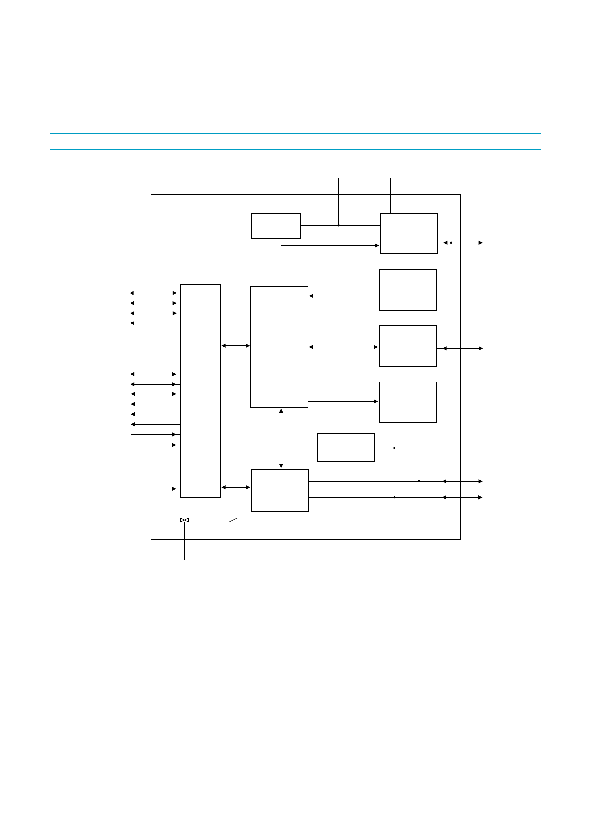
6. Block diagram
ISP1301
USB OTG transceiver
SCL
SDA
ADR/PSW
INT_N
OE_N/INT_N
DAT/VP
SE0/VM
RCV
VP
VM
SPEED
SUSPEND
V
DD_LGC
24
V
REG(3V3)
720
3.3 V DC-DC
REGULATOR
V
BAT
C2 C1
22 21
V
BUS
CHARGE PUMP
23
19
CGND
V
BUS
ISP1301
V
3
2
1
5
SERIAL
CONTROLLER
9
14
13
12
11
10
6
8
LEVEL
SHIFTER
CARKIT
INTERRUPT
DETECTOR
BUS
COMPARATORS
ID DETECTOR
PULL-UP AND
PULL-DOWN
RESISTORS
18
ID
RESET_N
Fig 1. Block diagram.
4
exposed die pad
DGND AGND
TRANSCEIVER
17
USB
15
16
004aaa195
DM
DP
9397 750 11355
© Koninklijke Philips Electronics N.V. 2004. All rights reserved.
Product data Rev. 01 — 14 April 2004 3 of 46
Page 4
Philips Semiconductors
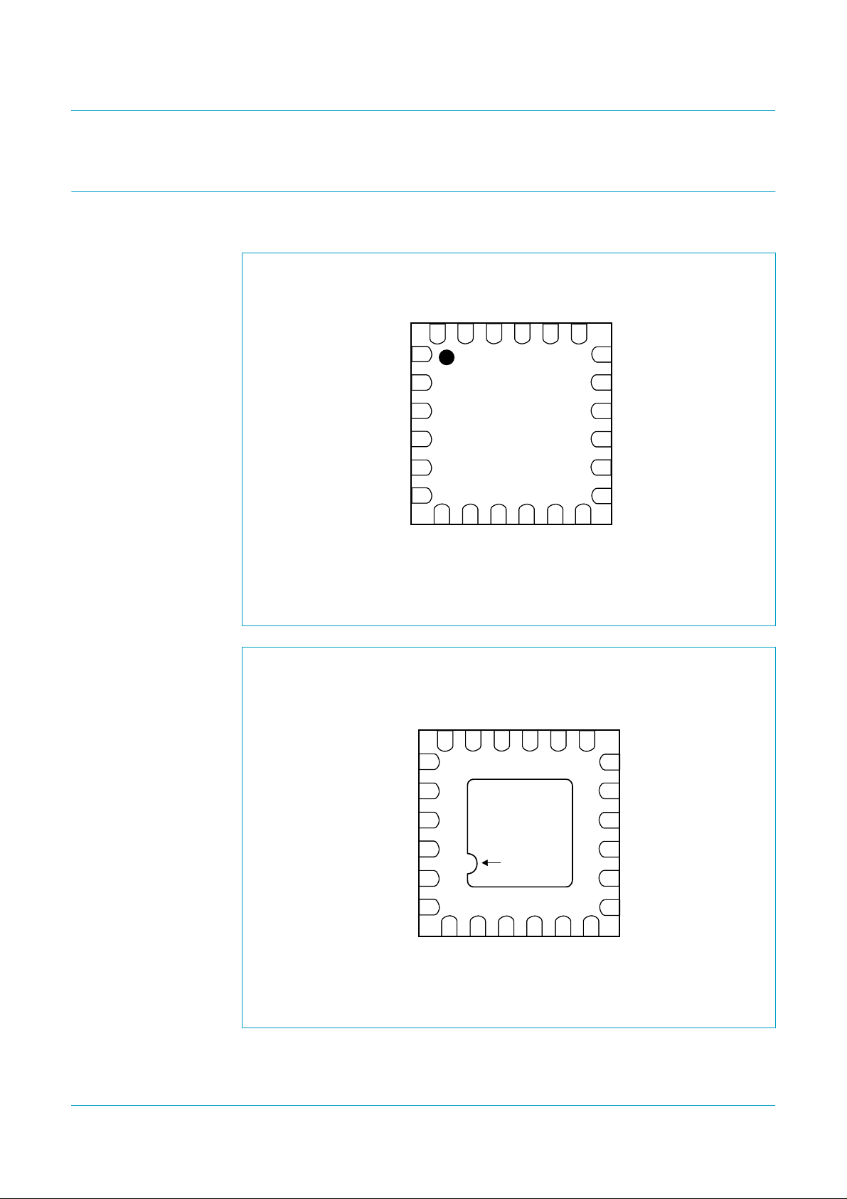
7. Pinning information
7.1 Pinning
ISP1301
USB OTG transceiver
DD_LGC
ADR/PSW
SDA
SCL
RESET_N
INT_N
SPEED
1
2
3
4
5
6
V
24
7
REG(3V3)
V
CGND
23
ISP1301BS
8
SUSPEND
C2
22 21 20
9 10 11
OE_N/INT_N
Fig 2. Pin configuration HVQFN24 (top view).
REG(3V3)
SUSPEND
SPEED
V
7
6
OE_N/INT_N
8
91011
C1
VM
VM
BAT
V
VP
VP
BUS
V
19
ID
18
AGND
17
16
DP
DM
15
DAT/VP
14
13
SE0/VM
12
004aaa542
RCV
RCV
12
SE0/VM
13
INT_N
RESET_N
SCL
SDA
ADR/PSW
Bottom view
5
4
3
2
1
24
DD_LGC
V
DGND
(exposed die pad)
ISP1301BS
terminal 1
23
22 21 20
C2
CGND
C1
BAT
V
DAT/VP
14
15
DM
DP
16
AGND
17
18
ID
19
004aaa196
BUS
V
Fig 3. Pin configuration HVQFN24 (bottom view).
9397 750 11355
Product data Rev. 01 — 14 April 2004 4 of 46
© Koninklijke Philips Electronics N.V. 2004. All rights reserved.
Page 5

Philips Semiconductors
7.2 Pin description
ISP1301
USB OTG transceiver
Table 2: Pin description
Symbol
ADR/PSW 1 I/O high-Z ADR input — sets the least-significant I
SDA 2 I/OD high-Z serial I
SCL 3 I/OD high-Z serial I
RESET_N 4 I - asynchronous reset; active LOW
INT_N 5 OD high-Z interrupt output; active LOW
SPEED 6 I - speed selection input for the ATX;effectivewhen
[2]
Pin Type
[1]
[3]
Reset
value
Description
2
C-bus
address bit of the ISP1301; latched-on reset
(including power-on reset)
PSW output — enables or disables the external
charge pump after reset
bidirectional; push-pull input; three-state output
2
C-bus data input and output
bidirectional; push-pull input; open-drain output
2
C-bus clock input and output
bidirectional; push-pull input; open-drain output
push-pull input
open-drain output
bit SPD_SUSP_CTRL = 0:
• LOW: low-speed
• HIGH: full-speed.
push-pull input
V
REG(3V3)
SUSPEND 8 I - suspend selection input for ATX; effective when
7 P - output of the internal voltage regulator; an
external decoupling capacitor of 0.1 µF is
required
bit SPD_SUSP_CTRL = 0:
• LOW: normal operating
• HIGH: suspend.
push-pull input
OE_N/
INT_N
VM 10 O - single-ended DM receiver output
VP 11 O - single-ended DP receiver output
RCV 12 O 0 differential receiver output; reflects the
9 I/O high-Z OE_N input — enable driving DP and DM when
in the USB mode
INT_N output — interrupt (push pull) when
suspended and bit OE_INT_EN = 1
bidirectional; push-pull input; three-state output
push-pull output
push-pull output
differential value of DP and DM
push-pull output
9397 750 11355
Product data Rev. 01 — 14 April 2004 5 of 46
© Koninklijke Philips Electronics N.V. 2004. All rights reserved.
Page 6

Philips Semiconductors
Table 2: Pin description
Symbol
SE0/VM 13 I/O -
DAT/VP 14 I/O -
DM 15 AI/O - USB data minus pin (D−)
DP 16 AI/O - USB data plus pin (D+)
AGND 17 P - analog ground
ID 18 AI/O - identification detector input and output;
V
BUS
V
BAT
C1 21 AI/O - charge pump capacitor pin 1; typically use a
C2 22 AI/O - charge pump capacitor pin 2; typically use a
CGND 23 P - ground for the charge pump
V
DD_LGC
DGND exposed
ISP1301
USB OTG transceiver
[1]
…continued
[2]
Pin Type
19 AI/O - V
20 P - supply voltage (2.7 V to 4.5 V)
24 P - supply voltage for the interface logic signals
die pad
[3]
Reset
Description
value
[4]
SE0 (input and output) — SE0 function in
DAT_SE0 USB mode
VM (input and output) — VM function in
VP_VM USB mode
bidirectional; push-pull input; three-state output
[4]
DAT (input and output) — DAT function in
DAT_SE0 USB mode
VP (input and output) — VP function in VP_VM
USB mode
bidirectional; push-pull input; three-state output
connected to the ID pin of the USB mini
receptacle
line input and output of the USB interface;
BUS
place an external decoupling capacitor of 0.1 µF
close to this pin
100 nF capacitor between pins C1 and C2
100 nF capacitor between pins C1 and C2
(1.65 V to 3.6 V)
P - digital ground
[1] A detailed description of these pins can be found in Section 8.9.
[2] Symbol names ending with underscore N (for example, NAME_N) indicate active LOW signals.
[3] I = input; O = output; I/O = digital input/output; OD = open-drain output; AI/O = analog input/output;
P = power or ground pin.
[4] High-Z when pin OE_N/INT_N is LOW. Driven LOW when pin OE_N/INT_N is HIGH.
9397 750 11355
Product data Rev. 01 — 14 April 2004 6 of 46
© Koninklijke Philips Electronics N.V. 2004. All rights reserved.
Page 7

Philips Semiconductors
8. Functional description
8.1 Serial controller
The serial controller includes the following functions:
2
• I
C-bus slave interface
• Interrupt generator
• Mode Control registers
• OTG registers
• Interrupt related registers
• Device identification registers.
The serial controller acts as an I2C-bus slave, and uses the SCL and SDA pins to
communicate with the OTG controller.
For more details on serial controller, see Section 11.
ISP1301
USB OTG transceiver
8.2 V
charge pump
BUS
The charge pump supplies current to the V
following modes:
• Output 5 V at current greater than 8 mA
• Pull-up V
• Pull-down V
before initiating SRP.
8.3 V
8.3.1 V
8.3.2 Session valid comparator
comparators
BUS
V
comparators provide indications regarding the voltage level on V
BUS
valid comparator
BUS
This comparator is used by an A-device to determine whether or not the voltage on
V
is at a valid level for operation. The minimum threshold for the V
BUS
comparator is 4.4 V. Any voltage on V
fault. During power up, it is expected that the comparator output will be ignored.
The session valid comparator is a TTL-level input that determines when V
enough for a session to start. Both the A-device and the B-device use this comparator
to detect when a session is being started. The A-device also uses this comparator to
indicate when a session is completed. The session valid threshold of the ISP1301 is
between 0.8 Vand 2.0 V.
to 3.3 V through a resistor (R
BUS
to ground through a resistor (R
BUS
line. It can operate in any of the
BUS
VBUS(PU)
below this threshold is considered to be a
BUS
) for initiating V
VBUS(PD)
) for discharging V
pulsing SRP
BUS
.
BUS
valid
BUS
BUS
BUS
is high
8.3.3 Session end comparator
The session end comparator determines when V
is below the B-device session
BUS
end threshold of 0.2 V to 0.8 V.
9397 750 11355
Product data Rev. 01 — 14 April 2004 7 of 46
© Koninklijke Philips Electronics N.V. 2004. All rights reserved.
Page 8

Philips Semiconductors
8.4 ID detector
In either the active or suspended power mode, the ID detector senses the condition of
the ID line and differentiates between the following three conditions:
• Pin ID is floating; bit ID_FLOAT = 1
• Pin ID is shorted to ground; bit ID_GND = 1
• Pin ID is connected to ground through resistor R
The ID detector also has a switch that can be used to ground pin ID. This switch is
controlled by bit ID_PULLDOWN in the serial controller.
8.5 Pull-up and pull-down resistors
The pull-up and pull-down resistors include the following switchable resistors:
• Pin DP pull-up
• Pin DP pull-down
• Pin DM pull-up
• Pin DM pull-down.
ID_GND = 0.
ISP1301
USB OTG transceiver
; bit ID_FLOAT = 0 and bit
ACC_ID
The pull-up resistor is a context variable as described in the
document. The variable pull-up resistor hardware is implemented to meet the USB
ECN_27% specification.
ECN_27%_Resistor
8.6 USB transceiver (ATX)
The behavior of the USB transceiver depends on the operation mode of the ISP1301:
• In the USB mode, the USB transceiver block performs USB full-speed or
low-speed transceiver functions. This includes differential driver, differential
receiver and single-ended receivers.
• In the transparent general purpose buffer mode or the UART mode, the USB
transceiverblockfunctions as a level shifter between the pins DAT/VP and SE0/VM
and the pins DP and DM.
8.7 3.3 V DC-DC regulator
The built-in 3.3 V DC-DC regulator conditions the supply voltage (V
ISP1301:
• V
• V
The output of the regulator can be monitored on the V
= 3.6 V to 4.5 V: the regulator will output 3.3 V ± 10 %
BAT
< 3.6 V: the regulator will be bypassed.
BAT
REG(3V3)
pin.
) for use in the
BAT
8.8 Car kit interrupt detector
The car kit interrupt detector is a comparator that detects when the DP line is below
the car kit interrupt threshold V
detector is enabled in the audio mode only (bit AUDIO_EN = 1).
9397 750 11355
Product data Rev. 01 — 14 April 2004 8 of 46
PH_CR_INT
(0.4 V to 0.6 V). The car kit interrupt
© Koninklijke Philips Electronics N.V. 2004. All rights reserved.
Page 9
Philips Semiconductors
8.9 Detailed description of pins
8.9.1 ADR/PSW
The ADR/PSW pin has two functions. On reset (including power-on reset), the level
on this pin is latched as ADR_REG, which represents the least significant bit (LSB) of
the I2C address of the ISP1301. If bit ADR_REG = 0, the I2C-bus address for the
ISP1301 is 0101100 (0x2C); if bit ADR_REG = 1, the I2C-bus address for the
ISP1301 is 0101101 (0x2D).
After reset, the ADR/PSW pin can be programmed as an output. If in the Mode
Control 2 register bit PSW_OE = 1, then the ADR/PSW output will be enabled. The
logic level will be determined by bit ADR_REG. If bit ADR_REG = 0, then the
ADR/PSW pin will drive HIGH. If bit ADR_REG = 1, then the ADR/PSW pin will drive
LOW.
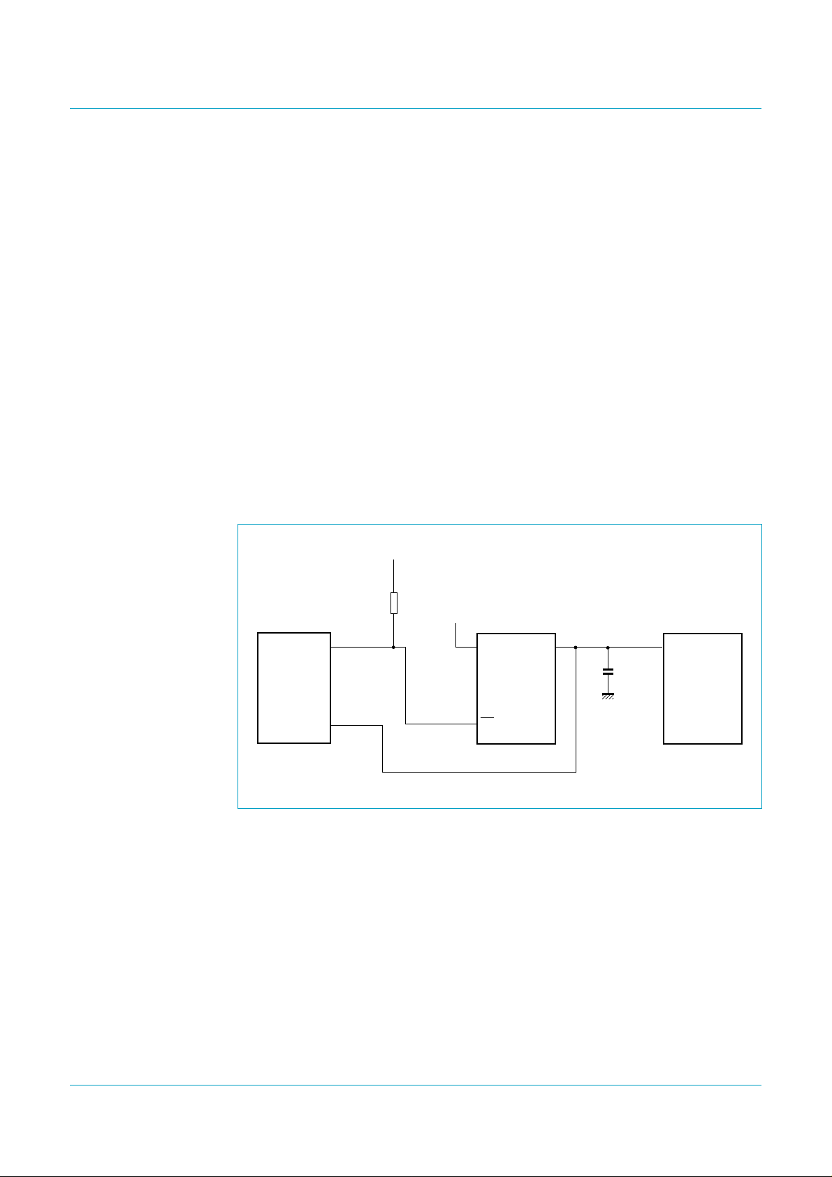
The ADR/PSW pin can be used to turn on or off the external charge pump. The
ISP1301 built-in charge pump supports V
more current support (for example, 50 mA), an external charge pump may be
needed. In this case, the ADR/PSW pin can act as a power switch for the external
charge pump. Figure 4 shows an example of using external charge pump.
ISP1301
USB OTG transceiver
current at 8 mA. If the application needs
BUS
ISP1301
Fig 4. Using external charge pump.
8.9.2 SCL and SDA
The SCL (serial clock) and SDA (serial data) signals implement a two-wire serial
I2C-bus.
8.9.3 RESET_N
Active LOW asynchronous reset for all digital logic. Either connect this pin to V
for power-on reset or apply a minimum of 10 µs LOW pulse for hardware reset.
ADR/PSW
V
BUS
+3.3 V
100 kΩ
V
BAT
V
CHARGE PUMP
ON/OFF
V
IN
OUT
4.7 µF
V
BUS
ID
DM
DP
GND
004aaa437
DD_LGC
8.9.4 INT_N
The INT_N (interrupt) pin is asserted while an interrupt condition exists. It is
deasserted when the Interrupt Latch register is cleared. The INT_N pin is open-drain,
and, therefore, can be connected using a wired-AND with other interrupt signals.
9397 750 11355
Product data Rev. 01 — 14 April 2004 9 of 46
© Koninklijke Philips Electronics N.V. 2004. All rights reserved.
Page 10

Philips Semiconductors
8.9.5 OE_N/INT_N
Pin OE_N/INT_N is normally an input to the ISP1301.
When bit TRANSP_EN = 0 and bit UART_EN = 0, the OE_N/INT_N pin controls the
direction of DAT/VP, SE0/VM, DP and DM as indicated in Table 4.
When suspended (either pin SUSPEND = HIGH or bit SUSPEND_REG = 1) and bit
OE_INT_EN = 1, pin OE_N/INT_N becomes a push-pull output (active LOW) to
indicate the interrupt condition.
8.9.6 SE0/VM, DAT/VP, RCV, VM and VP
The ISP1301 transmits USB data on the USB line under the following conditions:
• Bit TRANSP_EN = 0
• Bit UART_EN = 0
• Pin OE_N/INT_N = LOW.
Table 10 shows the operation of the SE0/VM and DAT/VP pins during the transmit
operation. The RCV pin is not used during transmit.
ISP1301
USB OTG transceiver
The ISP1301 receives USB data from the USB line under the following conditions:
• Bit TRANSP_EN = 0
• Bit UART_EN = 0
• Pin OE_N/INT_N = HIGH.
Table 12 shows the operation of the SE0/VM, DAT/VP and RCV pins during the
receive operation.
The VP and VM pins are single-ended receiver outputs of the DP and DM pins,
respectively.
8.9.7 DP and DM
The DP (data plus) and DM (data minus) pins implement the USB data signals. When
in the transparent general-purpose buffer mode, the ISP1301 operates as a level
shifter between the (DAT/VP, SE0/VM) and (DP, DM) pins.
8.9.8 ID
The ID (identification) pin is connected to the ID pin on the USB mini receptacle. An
internal pull-up resistor (to V
ID_PULLDOWN is set, the ID pin will be shorted to ground.
8.9.9 V
BUS
This pin acts as an input to the V
REG(3V3)
BUS
) is connected to this pin. When bit
comparator or an output from the charge pump.
When the VBUS_DRV bit of the OTG Control register is asserted, the ISP1301 tries
to drive V
least 8 mA.
9397 750 11355
Product data Rev. 01 — 14 April 2004 10 of 46
to a voltage of 4.4 V to 5.25 V with an output current capability of at
BUS
© Koninklijke Philips Electronics N.V. 2004. All rights reserved.
Page 11
Philips Semiconductors
ISP1301
USB OTG transceiver
8.9.10 V
BAT
This pin is an input and supplies power to the ISP1301. The ISP1301 operates when
V
is between 2.7 V and 4.5 V.
BAT
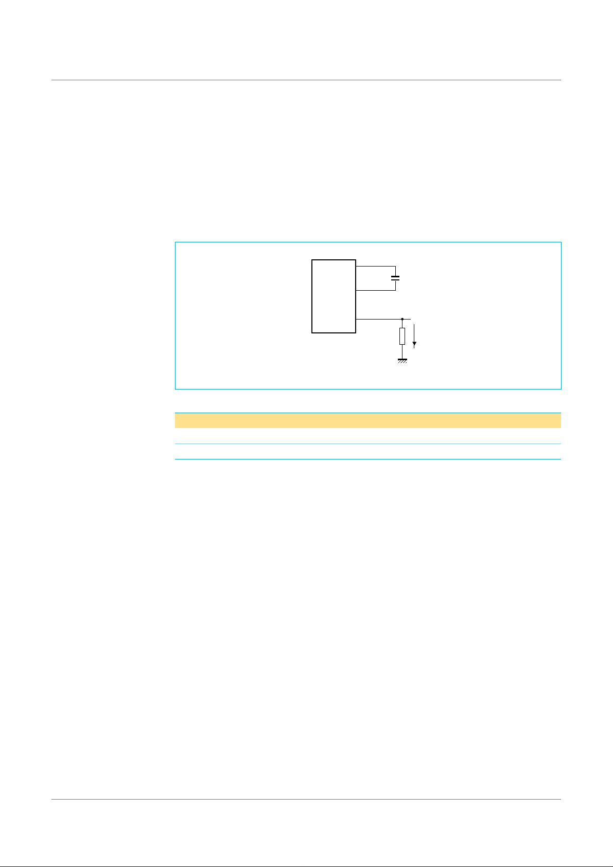
8.9.11 C1 and C2
The C1 and C2 pins are for connecting the flying capacitor of the charge pump. The
output current capacity of the charge pump depends on the value of the capacitor.
For maximum efficiency, place capacitors as close as possible to the pins.
Fig 5. Charge pump capacitor.
Table 3: Recommended charge pump capacitor value
C
ext
47 nF 8 mA
100 nF 18 mA
ISP1301
004aaa278
C1
C2
V
BUS
IL (max)
C
ext
I
L
[1]
[2]
8.9.12 V
[1] For output voltage V
[2] For V
DD_LGC
= 3.0 V to 4.5 V.
BAT
> 4.7 V (bit VBUS_VLD = 1).
BUS
This pin is an input and sets logic thresholds. It also powers the pads of the following
logic pins:
• ADR/PSW
• DAT/VP, SE0/VM and RCV
• VM and VP
• INT_N
• OE_N/INT_N
• RESET_N
• SPEED
• SUSPEND
• SCL and SDA.
8.9.13 AGND, CGND and DGND
AGND, CGND and DGND are ground pins for analog, charge pump and digital
circuits, respectively. These pins can be connected separately or together depending
on the system performance requirements.
9397 750 11355
Product data Rev. 01 — 14 April 2004 11 of 46
© Koninklijke Philips Electronics N.V. 2004. All rights reserved.
Page 12

Philips Semiconductors
9. Modes of operation
There are four types of modes in the ISP1301:
• Power modes
• Direct I
• USB modes
• Transparent modes.
9.1 Power modes
The power modes of the ISP1301 are as follows:
• Active power mode: power is on.
• USB suspend mode: to reduce power consumption, the USB differential receiver is
powered down.
• Global power-down mode: set bit GLOBAL_PWR_DN = 1 of the Mode Control 2
register; the differential transmitter and receiver, clock generator, charge pump,
and all biasing circuits are turned off to reduce power consumption to the minimum
possible; for details on waking up the clock, see Section 12.
2
C-bus mode
ISP1301
USB OTG transceiver
9.2 Direct I2C-bus mode
In the direct I2C-bus mode, an external I2C-bus master (OTG controller) directly
communicates with the serial controller through the SCL and SDA lines. The serial
controller has a built-in I2C-bus slave function.
In this mode, an external I2C-bus master can access the internal registers of the
device (Status, Control, Interrupt, and so on) through the I2C-bus interface.
The supported I2C-bus bit rate is 100 kbit/s (maximum).
The ISP1301 is in the direct I2C-bus mode when either bit TRANSP_EN bit = 0 or pin
OE_N/INT_N is deasserted.
9.3 USB modes
The four USB modes of the ISP1301 are:
• VP_VM unidirectional mode
• VP_VM bidirectional mode
• DAT_SE0 unidirectional mode
• DAT_SE0 bidirectional mode.
In the VP_VM USB mode, the DAT/VP pin is used for the VP function, the SE0/VM
pin is used for the VM function, and the RCV pin is used for the RCV function.
In the DAT_SE0 USB mode, the DAT/VP pin is used forthe DAT function, the SE0/VM
pin is used for the SE0 function, and the RCV pin is not used.
In the unidirectional mode, the DAT/VP and SE0/VM pins are always inputs. In the
bidirectional mode, the direction of these signals depends on the OE_N/INT_N input.
9397 750 11355
Product data Rev. 01 — 14 April 2004 12 of 46
© Koninklijke Philips Electronics N.V. 2004. All rights reserved.
Page 13

Philips Semiconductors
Table 6 specifies the functionality of the device during the four USB modes.
The ISP1301 is in the USB mode when both the TRANSP_EN and UART_EN bits
are cleared.
9.4 Transparent modes
9.4.1 Transparent general-purpose buffer mode
In the transparent general-purpose buffer mode, the DAT/VP and SE0/VM pins are
connected to the DP and DM pins, respectively. Using bits TRANSP_BDIR1 and
TRANSP_BDIR0 of the Mode Control 2 register as specified in Table 8, you can
control the direction of data transfer. The ISP1301 is in the transparent
general-purpose buffer mode if bit TRANSP_EN = 1 and bit DAT_SE0 = 1.
9.4.2 Transparent UART mode
When in the transparent UART mode, the ATX behaves as two logic level translator
between the following pins:
ISP1301
USB OTG transceiver
• For TxD signal: from SE0/VM (V
• For RxD signal: from DP (+3.3 V level) to DAT/VP (V
level) to DM (+3.3 V level)
DD_LGC
DD_LGC
level).
In the UART mode, the OTG controller is allowed to connect a UART to the DAT/VP
and SE0/VM pins of the ISP1301.
The UART mode is entered by setting the UART_EN bit in the Mode Control 1
register. The UART mode is equivalent to one of the transparent general purpose
buffer mode (bit TRANSP_BDIR1 = 1, bit TRANSP_BDIR0 = 0).
9.4.3 Summary tables
Table 4: Device operating modes
Mode USB
suspend
condition
Direct I
Direct I
USB modes
USB suspend mode 1 X X 0 0 see Table 5 and Table 7
USB functional mode 0 X X 0 0 ATX is fully functional; seeTable 6
Transparent modes
Transparent general-purpose
buffer mode
Transparent UART mode X X X X 1 DAT/VP <= DP (RxD signal of UART)
2
C-bus mode
2
C-bus mode X X X 0 X
X X HIGH 1 X
X1X1X
X 1 X 1 0 ATX is not functional; see Table 8
Bit
DAT
[1]
_SE0
Pin
OE_N/
INT_N
Bit
TRANSP
_EN
Bit
UART
_ EN
Description
SE0/VM => DM (TxD signal of UART);
ATX is not functional
[1] Conditions:
a) bit SPD_SUSP_CTRL = 0 and pin SUSPEND = HIGH, or
b) bit SPD_SUSP_CTRL = 1 and bit SUSPEND_REG = 0.
9397 750 11355
Product data Rev. 01 — 14 April 2004 13 of 46
© Koninklijke Philips Electronics N.V. 2004. All rights reserved.
Page 14

Philips Semiconductors
Table 5: USB suspend mode: I/O
Pin Function
DP as output can be driven if pin OE_N/INT_N is active LOW, otherwise high-Z
DM as output can be driven if pin OE_N/INT_N is active LOW, otherwise high-Z
V
BUS
SCL connected to SCL I/O of the I
SDA connected to SDA I/O of the I
[1] In the USB suspend mode, the ISP1301 can drive the DP and DM lines, if the OE_N/INT_N input
ISP1301
USB OTG transceiver
[1]
[1]
can be driven depending on bit VBUS_DRV
2
C-bus slave
2
C-bus slave
(when the OE_INT_EN bit is not set) is LOW. In such a case, these outputs are driven as in the USB
functional modes, but with the full-speed characteristics, irrespective of the value of the SPEED input
pin or the SPEED_REG bit.
Table 6: USB functional modes: I/O values
[1]
USB mode Bit Pin
DAT_SE0 BI_DI OE_N/
DAT/VP SE0/VM VP VM RCV
INT_N
VP_VM unidirectional 0 0 X TxD+
bidirectional 0 1 LOW TxD+
0 1 HIGH RxD+
DAT_SE0 unidirectional 1 0 X TxD
bidirectional 1 1 LOW TxD
1 1 HIGH RxD
[1] Some of the modes and signals are provided to achieve backward compatibility with IP cores.
[2] TxD+ and TxD− are single-ended inputs for driving the DP and DM outputs, respectively, in the single-ended mode.
[3] RxD+ and RxD− are the outputs of the single-ended receivers connected to DP and DM, respectively.
[4] TxD is the input for driving DP and DM in the DAT_SE0 mode.
[5] FSE0 is for forcing an SE0 on the DP and DM lines in the DAT_SE0 mode.
[6] RxD is the output of the differential receiver.
[7] RSE0 is an output indicating that an SE0 has been received on the DP and DM lines.
[2]
[2]
[3]
[4]
[4]
[6]
TxD−
TxD−
RxD−
FSE0
FSE0
RSE0
[2]
[2]
[3]
[5]
[5]
[7]
RxD+
[3]
RxD−
Table 7: USB suspend mode: I/O values
USB suspend mode Input pin Output pin
DP DM DAT/VP SE0/VM VP VM RCV
DAT_SE0
(bit DAT_SE0 = 1)
LOW LOW LOW HIGH LOW LOW LOW
HIGH LOW HIGH LOW HIGH LOW LOW
LOW HIGH LOW LOW LOW HIGH LOW
HIGH HIGH HIGH LOW HIGH HIGH LOW
VP_VM
(bit DAT_SE0 = 0)
LOW LOW LOW LOW LOW LOW LOW
HIGH LOW HIGH LOW HIGH LOW LOW
LOW HIGH LOW HIGH LOW HIGH LOW
HIGH HIGH HIGH HIGH HIGH HIGH LOW
[3]
RxD
[3]
9397 750 11355
Product data Rev. 01 — 14 April 2004 14 of 46
© Koninklijke Philips Electronics N.V. 2004. All rights reserved.
Page 15

Philips Semiconductors
Table 8: Transparent general-purpose buffer mode
Bit
TRANSP_BDIR[1:0]
00 DAT/VP => DP SE0/VM => DM
01 DAT/VP => DP SE0/VM <= DM
10 DAT/VP <= DP SE0/VM => DM
11 DAT/VP <= DP SE0/VM <= DM
10. USB transceiver
10.1 Differential driver
The operation of the driver is described in Table 9. The register bits and the pins used
in the column heading are described in Section 11.1 and Section 8.9, respectively.
Table 9: Transceiver driver operation setting
Suspend
0 0 LOW 0 output value from DAT/VP to DP and
0 0 LOW 1 output value from DAT/VP to DP and DM
1 0 LOW X output value from DAT/VP to DP and DM
X X HIGH X high-Z
X 1 X X high-Z
[1]
Bit
TRANSP_
EN
Direction of the data flow
Pin
OE_N/
INT_N
Bit
DAT_SE0
ISP1301
USB OTG transceiver
Differential driver
SE0/VM to DM
if SE0/VM is 0; otherwise, drive both DP
and DM LOW
[1] Can be controlled by using either the SUSPEND pin or the SUSPEND_REG bit.
Table 10: USB functional mode: transmit operation
USB mode Input pin Output pin
DAT/VP SE0/VM DP DM
DAT_SE0 LOW LOW LOW HIGH
HIGH LOW HIGH LOW
LOW HIGH LOW LOW
HIGH HIGH LOW LOW
VP_VM LOW LOW LOW LOW
HIGH LOW HIGH LOW
LOW HIGH LOW HIGH
HIGH HIGH HIGH HIGH
10.2 Differential receiver
Table 11 describes the operation of the differential receiver. The register bits and the
pins used in the column heading are described in Section 11.1 and Section 8.9,
respectively.
9397 750 11355
Product data Rev. 01 — 14 April 2004 15 of 46
© Koninklijke Philips Electronics N.V. 2004. All rights reserved.
Page 16

Philips Semiconductors
The detailed behavior of the receive transceiver operation is given in Table 12.
Table 11: Differential receiver operation settings
Suspend
1X X X0
X X LOW X 0
X1 X X0
0 0 HIGH 1 output differential value from DP
0 0 HIGH 0 output differential value from DP
[1] Can be controlled by using either the SUSPEND pin or the SUSPEND_REG bit.
Table 12: USB functional mode: receive operation
USB mode Suspend
DAT_SE0 0 LOW LOW RCV HIGH last value of RCV
DAT_SE0 0 HIGH LOW HIGH LOW HIGH
DAT_SE0 0 LOW HIGH LOW LOW LOW
DAT_SE0 0 HIGH HIGH RCV LOW last value of RCV
DAT_SE0 1 LOW LOW LOW HIGH LOW
DAT_SE0 1 HIGH LOW HIGH LOW LOW
DAT_SE0 1 LOW HIGH LOW LOW LOW
DAT_SE0 1 HIGH HIGH HIGH LOW LOW
VP_VM 0 LOW LOW LOW LOW last value of RCV
VP_VM 0 HIGH LOW HIGH LOW HIGH
VP_VM 0 LOW HIGH LOW HIGH LOW
VP_VM 0 HIGH HIGH HIGH HIGH last value of RCV
VP_VM 1 LOW LOW LOW LOW LOW
VP_VM 1 HIGH LOW HIGH LOW LOW
VP_VM 1 LOW HIGH LOW HIGH LOW
VP_VM 1 HIGH HIGH HIGH HIGH LOW
[1]
Bit
TRANSP_EN
Pin
OE_N/INT_N
[1]
Input pin Output pin
DP DM DAT/VP SE0/VM RCV
Bit
DAT_SE0
Differential receiver
and DM to DAT/VP and RCV
and DM to RCV
ISP1301
USB OTG transceiver
[1] Can be controlled by using either the SUSPEND pin or the SUSPEND_REG bit.
9397 750 11355
Product data Rev. 01 — 14 April 2004 16 of 46
© Koninklijke Philips Electronics N.V. 2004. All rights reserved.
Page 17

Philips Semiconductors
ISP1301
USB OTG transceiver
11. Serial controller
11.1 Register map
Table 13 provides an overview of the serial controller registers.
Table 13: Serial controller registers
Register Width
(bits)
Vendor ID 16 R 00–01H device identification registers Section 11.1.1 on page 17
Product ID 16 R 02–03H
Version ID 16 R 14–15H
Mode Control 1 8 R/S/C Set — 04H
Mode Control 2 8 R/S/C Set — 12H
OTG Control 8 R/S/C Set — 06H
OTG Status 8 R 10H
Interrupt Source 8 R 08H interrupt related registers Section 11.1.4 on page 20
Interrupt Latch 8 R/S/C Set — 0AH
Interrupt Enable Low 8 R/S/C Set — 0CH
Interrupt Enable High 8 R/S/C Set — 0EH
Access
[1]
Memory address Functionality Reference
mode control registers Section 11.1.2 on page 18
Clear — 05H
Clear — 13H
OTG registers Section11.1.3 on page 19
Clear — 07H
Clear — 0BH
Clear — 0DH
Clear — 0FH
[1] The R/S/C access type represents a field that can be read, set or cleared (set to 0). A register can be read from either of the indicated
addresses—set or clear. Writing logic 1 to the set address causes the associated bit to be set. Writing logic 1 to the clear address
causes the associated bit to be cleared. Writing logic 0 to an address has no effect.
11.1.1 Device identification registers
Vendor ID register (Read: 00H–01H): Table 14 provides the bit allocation of the
Vendor ID register.
Table 14: Vendor ID register: bit description
Bit Symbol Access Value Description
15 to 0 VENDORID
[15:0]
R 04CCH Philips Semiconductors’ Vendor ID
Product ID register (Read: 02H–03H): The bit allocation of this register is given in
Table 15.
Table 15: Product ID register: bit description
Bit Symbol Access Value Description
15 to 0 PRODUCTID
[15:0]
9397 750 11355
Product data Rev. 01 — 14 April 2004 17 of 46
R 1301H Product ID of the ISP1301
© Koninklijke Philips Electronics N.V. 2004. All rights reserved.
Page 18

Philips Semiconductors
ISP1301
USB OTG transceiver
Version ID register (Read: 14H–15H): Table 16 shows the bit allocation of this
register.
Table 16: Version ID register: bit description
Bit Symbol Access Value Description
15 to 0 VERSIONID
[15:0]
R 0210H Version number of the ISP1301
11.1.2 Mode control registers
Mode Control 1 register (Set/Clear: 04H/05H): The bit allocation of the Mode
Control 1 register is given in Table 17.
Table 17: Mode Control 1 register: bit allocation
Bit 7 6 5 4 3 2 1 0
Symbol - UART_EN OE_INT_
EN
Reset -0000000
Access R/S/C R/S/C R/S/C R/S/C R/S/C R/S/C R/S/C R/S/C
BDIS_
ACON_EN
TRANSP_ENDAT_SE0 SUSPEND
_REG
SPEED_
REG
Table 18: Mode Control 1 register: bit description
Bit Symbol Description
7 - reserved
6 UART_EN When set, the ATX is in the transparent UART mode.
5 OE_INT_EN When set and when in the suspend mode, pin OE_N/INT_N
becomes an output and is asserted when an interrupt occurs.
4 BDIS_ACON_EN Enables the A-device to connect if the B-device disconnect is
detected; see Section 11.3
3 TRANSP_EN When set, the ATX is in the transparent mode.
2 DAT_SE0 0 — VP_VM mode
1 — DAT_SE0 mode; see Table 6 and Table 7
1 SUSPEND_REG Sets the ISP1301 in the suspend mode, if bit
SPD_SUSP_CTRL = 1.
0 — active-power mode
1 — USB suspend mode
0 SPEED_REG Sets the rise time and the fall time of the transmit driver in
USB modes, if bit SPD_SUSP_CTRL = 1.
0 — USB low-speed mode
1 — USB full-speed mode
Mode Control 2 register (Set/Clear: 12H/13H): For the bit allocation of this register,
see Table 19.
9397 750 11355
Product data Rev. 01 — 14 April 2004 18 of 46
© Koninklijke Philips Electronics N.V. 2004. All rights reserved.
Page 19

Philips Semiconductors
ISP1301
USB OTG transceiver
Table 19: Mode Control 2 register: bit allocation
Bit 7 6 5 4 3 2 1 0
Symbol EN2V7 PSW_OE AUDIO_EN TRANSP_
BDIR1
Reset 0000010 0
Access R/S/C R/S/C R/S/C R/S/C R/S/C R/S/C R/S/C R/S/C
Table 20: Mode Control 2 register: bit description
Bit Symbol Description
7 EN2V7 0 — V
1 — V
6 PSW_OE 0 — ADR/PSW pin acts as an input
1 — ADR/PSW pin is driven
5 AUDIO_EN 0 — SE receiver is enabled; cr_int detector is disabled
1 — SE receiver is turned off (pin VP = LOW,pinVM = LOW);
cr_int detector is enabled
4 to 3 TRANSP_BDIR[1:0] controls the direction of data transfer in the transparent
general-purpose buffer mode; see Table 8
2 BI_DI 0 — direction of DAT/VP and SE0/VM are fixed (transmit only)
1 — direction of DAT/VP and SE0/VM are controlled by
pin OE_N/INT_N; see Table 6
1 SPD_SUSP_CTRL control of speed and suspend in USB modes:
TRANSP_
BDIR0
= 3.0 V to 4.5 V
BAT
= 2.7 V to 4.5 V
BAT
BI_DI SPD_SUSP
_CTRL
GLOBAL_
PWR_DN
0 — controlled by pins SPEED and SUSPEND
1 — controlled by bit SPEED_REG and bit SUSPEND_REG
of the Mode Control 1 register
0 GLOBAL_PWR_DN 0 — normal operation
1 — sets the ISP1301 to the power down mode
2
Activities on the I
chip; see Section 12
C-bus or any OTG event can wake up the
11.1.3 OTG registers
OTG Control register (Set/Clear: 06H/07H): Table 21 provides the bit allocation of
the OTG Control register.
Table 21: OTG Control register: bit allocation
Bit 7 6 5 4 3 2 1 0
Symbol VBUS_
CHRG
Reset 00001100
Access R/S/C R/S/C R/S/C R/S/C R/S/C R/S/C R/S/C R/S/C
VBUS_
DISCHRG
VBUS_
DRV
ID_PULL
DOWN
DM_PULL
DOWN
DP_PULL
DOWN
DM_PULLUPDP_PULL
UP
9397 750 11355
Product data Rev. 01 — 14 April 2004 19 of 46
© Koninklijke Philips Electronics N.V. 2004. All rights reserved.
Page 20

Philips Semiconductors
ISP1301
USB OTG transceiver
Table 22: OTG Control register: bit description
Bit Symbol Description
7 VBUS_CHRG charge V
6 VBUS_DISCHRG discharge V
5 VBUS_DRV drive V
4 ID_PULLDOWN connect the ID pin to ground
3 DM_PULLDOWN connect DM pull-down resistor to ground
2 DP_PULLDOWN connect DP pull-down resistor to ground
1 DM_PULLUP connect DM pull-up resistor to 3.3 V
0 DP_PULLUP connect DP pull-up resistor to 3.3 V
through a resistor to 3.3 V
BUS
through a resistor to ground
BUS
to 5 V through the charge pump
BUS
OTG Status register (Read: 10H): Table 23 shows the bit allocation of the OTG
Status register.
Table 23: OTG Status register: bit allocation
Bit 7 6 5 4 3 2 1 0
Symbol B_SESS_
VLD
Reset 00000000
Access RRRRRRRR
B_SESS_
END
reserved
Table 24: OTG Status register: bit description
Bit Symbol Description
7 B_SESS_VLD set when the V
threshold (2.0 V to 4.0 V)
6 B_SESS_END set when the V
threshold (0.2 V to 0.8 V)
5 to 0 - reserved
voltage is above the B-device session valid
BUS
voltage is below the B-device session end
BUS
11.1.4 Interrupt related registers
Interrupt Source register (Read: 08H): This register indicates the current state of
the signals that can generate an interrupt. The bit allocation of the Interrupt Source
register is given in Table 25.
Table 25: Interrupt Source register: bit allocation
Bit 7 6 5 4 3 2 1 0
Symbol CR_INT BDIS_
ACON
Reset 00000000
Access RRRRRRRR
ID_FLOAT DM_HI ID_GND DP_HI SESS_VLD VBUS_VLD
9397 750 11355
Product data Rev. 01 — 14 April 2004 20 of 46
© Koninklijke Philips Electronics N.V. 2004. All rights reserved.
Page 21

Philips Semiconductors
ISP1301
USB OTG transceiver
Table 26: Interrupt Source register: bit description
Bit Symbol Description
7 CR_INT DP pin is above the car kit interrupt threshold (0.4 V to 0.6 V)
6 BDIS_ACON set when bit BDIS_ACON_EN is set, and the ISP1301 asserts bit
DP_PULLUP after detecting the B-device disconnect
5 ID_FLOAT ID pin is floating
4 DM_HI DM pin is HIGH
3 ID_GND ID pin is connected to ground
2 DP_HI DP pin is HIGH
1 SESS_VLD session valid comparator; threshold = 0.8 V to 2.0 V
0 VBUS_VLD A-device V
valid comparator; threshold > 4.4 V
BUS
Interrupt Latch register (Set/Clear: 0AH/0BH): This register indicates the source
that generated the interrupt. The bit allocation of the Interrupt Latch register is given
in Table 27.
Table 27: Interrupt Latch register: bit allocation
Bit 7 6 5 4 3 2 1 0
Symbol CR_INT BDIS_
ACON
Reset 00000000
Access R/S/C R/S/C R/S/C R/S/C R/S/C R/S/C R/S/C R/S/C
ID_FLOAT DM_HI ID_GND DP_HI SESS_VLD VBUS_VLD
Table 28: Interrupt Latch register: bit description
Bit Symbol Description
7 CR_INT interrupt for CR_INT status change
6 BDIS_ACON interrupt for BDIS_ACON status change
5 ID_FLOAT interrupt for ID_FLOAT status change
4 DM_HI interrupt for DM_HI status change
3 ID_GND interrupt for ID_GND status change
2 DP_HI interrupt for DP_HI status change
1 SESS_VLD interrupt for SESS_VLD status change
0 VBUS_VLD interrupt for VBUS_VLD status change
Interrupt Enable Low register (Set/Clear: 0CH/0DH): This register enables
interrupts on transition from true to false. For the bit allocation of this register, see
Table 29.
Table 29: Interrupt Enable Low register: bit allocation
Bit 7 6 5 4 3 2 1 0
Symbol CR_INT BDIS_
ACON
Reset 00000000
Access R/S/C R/S/C R/S/C R/S/C R/S/C R/S/C R/S/C R/S/C
ID_FLOAT DM_HI ID_GND DP_HI SESS_VLD VBUS_VLD
9397 750 11355
Product data Rev. 01 — 14 April 2004 21 of 46
© Koninklijke Philips Electronics N.V. 2004. All rights reserved.
Page 22

Philips Semiconductors
ISP1301
USB OTG transceiver
Table 30: Interrupt Enable Low register: bit description
Bit Symbol Description
7 CR_INT interrupt enable for CR_INT status change from 1 to 0
6 BDIS_ACON interrupt enable for BDIS_ACON status change from 1 to 0
5 ID_FLOAT interrupt enable for ID_FLOAT status change from 1 to 0
4 DM_HI interrupt enable for DM_HI status change from 1 to 0
3 ID_GND interrupt enable for ID_GND status change from 1 to 0
2 DP_HI interrupt enable for DP_HI status change from 1 to 0
1 SESS_VLD interrupt enable for SESS_VLD status change from 1 to 0
0 VBUS_VLD interrupt enable for VBUS_VLD status change from 1 to 0
Interrupt Enable High register (Set/Clear: 0EH/0FH): The Interrupt Enable High
register enables interrupts on transition from FALSE to TRUE. Table 31 provides the
bit allocation of this register.
Table 31: Interrupt Enable High register: bit allocation
Bit 7 6 5 4 3 2 1 0
Symbol CR_INT BDIS_
ACON
Reset 00000000
Access R/S/C R/S/C R/S/C R/S/C R/S/C R/S/C R/S/C R/S/C
ID_FLOAT DM_HI ID_GND DP_HI SESS_VLD VBUS_VLD
Table 32: Interrupt Enable High register: bit description
Bit Symbol Description
7 CR_INT interrupt enable for CR_INT status change from 0 to 1
6 BDIS_ACON interrupt enable for BDIS_ACON status change from 0 to 1
5 ID_FLOAT interrupt enable for ID_FLOAT status change from 0 to 1
4 DM_HI interrupt enable for DM_HI status change from 0 to 1
3 ID_GND interrupt enable for ID_GND status change from 0 to 1
2 DP_HI interrupt enable for DP_HI status change from 0 to 1
1 SESS_VLD interrupt enable for SESS_VLD status change from 0 to 1
0 VBUS_VLD interrupt enable for VBUS_VLD status change from 0 to 1
11.2 Interrupts
Table 26 indicates the signals that can generate interrupts. Any of the signals given in
Table 26 can generate an interrupt when the signal becomes either LOW or HIGH.
After an interrupt has been generated, the OTG controller should be able to read the
status of each signal and the bit that indicates whether or not that signal generated
the interrupt.
A bit in the Interrupt Latch register is set when any of these occurs:
• Writing logic 1 to its set address causes the corresponding bit to be set
• The corresponding bit in the Interrupt Enable High register is set, and the
associated signal changes from LOW to HIGH
• The corresponding bit in the Interrupt Enable Low register is set, and the
associated signal changes from HIGH to LOW.
9397 750 11355
Product data Rev. 01 — 14 April 2004 22 of 46
© Koninklijke Philips Electronics N.V. 2004. All rights reserved.
Page 23

Philips Semiconductors
The Interrupt Latch register bit is cleared by writing logic 1 to its clear address.
11.3 Autoconnect
The Host Negotiation Protocol (HNP) in the OTG supplement specifies the following
sequence of events to transfer the role of the host from the A-device to the B-device:
1. The A-device puts the bus in the suspend state
2. The B-device simulates a disconnect by deasserting its DP pull-up
3. The A-device detects SE0 on the bus, and asserts its DP pull-up
4. The B-device detects that the DP line is HIGH, and takes the role of the host.
The OTG supplement specifies that the time between the B-device deasserting its DP
pull-up and the A-device asserting its pull-up must be less than 3 ms. For an A-device
with a slow interrupt response time, 3 ms maynot be enough time to write an I2C-bus
command to the ISP1301 to assert the DP pull-up. An alternative method is for the
A-device transceiver to automatically assert the DP pull-up after detecting an SE0
from the B-device.
ISP1301
USB OTG transceiver
The sequence of events is as follows:
After finishing data transfers between the A-device and the B-device and before
suspending the bus, the A-device sends SOFs. The B-device receives these SOFs,
and does not transmit any packet back to the A-device.During this time, the A-device
sets the BDIS_ACON_EN bit in the ISP1301. This enables the ISP1301 to look for
SE0 whenever the A-device is not transmitting (that is, whenever the OE_N/INT_N
pin of the ISP1301 is not asserted). After the BDIS_ACON_ENbit is set, the A-device
stops transmitting SOFs and allows the bus to go to the idle state. If the B-device
disconnects, the bus goes to SE0, and the ISP1301 logic automatically turns on the
A-device pull-up.
9397 750 11355
Product data Rev. 01 — 14 April 2004 23 of 46
© Koninklijke Philips Electronics N.V. 2004. All rights reserved.
Page 24

Philips Semiconductors
12. Clock wake up scheme
This section explains the ISP1301 clock stop timing, events triggering the clock to
wake up, and the timing of the clock wake up.
12.1 Power down event
The clock is stopped when the GLOBAL_PWR_DN bit is set. It takes approximately
8 ms for the clock to stop from the time the power down condition is detected. The
clock always stops at its falling edge. The waveform is given in Figure 6.
SCL
GLOBAL_PWR_DN
CLOCK
ISP1301
USB OTG transceiver
Fig 6. Clock stopped using the GLOBAL_PWR_DN bit.
12.2 Clock wake up events
The clock wakes up when any of the following events occur on the ISP1301 pins:
• SCL goes LOW
• V
goes above the session valid threshold (0.8 V to 2.0 V), provided the
BUS
SESS_VLD bit in the Interrupt Enable High register is set.
• ID changes when mini-A plug is inserted, provided the ID_FLOAT bit in the
Interrupt Enable Low register is set.
• ID changes when mini-A plug is removed, provided the ID_FLOAT bit in the
Interrupt Enable High register is set.
• DP goes HIGH, provided the DP_HI bit in the Interrupt Enable High register is set.
• DM goes HIGH, provided the DM_HI bit in the Interrupt Enable High register is set.
The event triggers the clock to start and a stable clock is guaranteed after about six
clock periods, which is approximately 8 µs. The startup analog clock time is 10 µs.
Therefore, the total estimated start time after a triggered event is about 20 µs. The
clock will always start at its rising edge.
8 ms
004aaa217
Waveforms of the clock wake up because of different events are given in Figure 7,
Figure 8, Figure 9, Figure 10 and Figure 11.
SCL
CLOCK
Fig 7. Clock wake up using SCL.
9397 750 11355
Product data Rev. 01 — 14 April 2004 24 of 46
20 µs
© Koninklijke Philips Electronics N.V. 2004. All rights reserved.
004aaa218
Page 25

Philips Semiconductors
SESS_VLD
CLOCK
20 µs
ISP1301
USB OTG transceiver
004aaa219
Fig 8. Clock wake up by V
ID_FLOAT
CLOCK
BUS
.
Fig 9. Clock wake up by ID change (1).
ID_FLOAT
CLOCK
Fig 10. Clock wake up by ID change (2).
DP_HI
or DM_HI
CLOCK
20 µs
20 µs
20 µs
004aaa220
004aaa221
004aaa434
Fig 11. Clock wake up by data line SRP.
When an event is triggered and the clock is started, it will remain active for 8 ms. If
the GLOBAL_PWR_DN bit is not cleared within this 8 ms period, the clock will stop. If
the clock wakes up because of any event other than SCL going LOW, an interrupt will
be generated once the clock is active.
9397 750 11355
Product data Rev. 01 — 14 April 2004 25 of 46
© Koninklijke Philips Electronics N.V. 2004. All rights reserved.
Page 26

Philips Semiconductors
13. I2C-bus protocol
ISP1301
USB OTG transceiver
For detailed information, refer to
The I2C-bus specification; version 2.1
13.1 I2C-bus byte transfer format
Table 33: I2C-bus byte transfer format
S Byte 1 A Byte 2 A Byte 3 A … A P
8 bits 8 bits 8 bits …
[1] S = Start; A = Acknowledge; P = Stop.
13.2 I2C-bus device address
Table 34: Device address byte 1
Bit 7 6 5 4 3 2 1 0
Name A6 A5 A4 A3 A2 A1 A0 R/W
Value 0 1 0 1 1 0 X X
Table 35: Bit description
Bit Symbol Description
7 to 1 A[6:0] Device address: The device address of the ISP1301 is: 0101 10 (A0).
The value of A0 (LSB) is loaded from pin ADR/PSW during reset
(including power-on reset). If pin ADR/PSW = HIGH, bit A0 = 1;
otherwise bit A0 = 0.
0 R/W Read/write command.
.
[1]
device address -
0 — write
1 — read.
13.3 Write format
A write operation can be performed as:
• One-byte write to the specified register address
• Multi-byte write to N consecutive registers, starting from the specified start
address. N defines the number of registers to write. If N = 1, only the start register
is written.
13.3.1 One-byte write
Figure 12 illustrates the byte sequence.
Table 36: Transfer format description for one-byte write
Byte Description
S master starts with a START condition
Device select master transmits device address and write command bit R/W = 0
ACK slave generates an acknowledgment
Register address K master transmits address of register K
9397 750 11355
Product data Rev. 01 — 14 April 2004 26 of 46
© Koninklijke Philips Electronics N.V. 2004. All rights reserved.
Page 27

Philips Semiconductors
ISP1301
USB OTG transceiver
Table 36: Transfer format description for one-byte write
Byte Description
ACK slave generates an acknowledgment
Write data K master writes data to register K
ACK slave generates an acknowledgment
P master generates a STOP condition
13.3.2 Multiple-byte write
Figure 12 illustrates the byte sequence.
Table 37: Transfer format description for multiple-byte write
Byte Description
S master starts with a START condition
Device select master transmits device address and write command bit R/W = 0
ACK slave generates an acknowledgment
Register address K master transmits address of register K. This is the start address for
ACK slave generates an acknowledgment
Write data K master writes data to register K
ACK slave generates an acknowledgment
Write data K + 1 master writes data to register K + 1
ACK slave generates an acknowledgment
::
Write data
K+N− 1
ACK slave generates an acknowledgment
P master generates a STOP condition
…continued
writing multiple data bytes to consecutive registers. After a byte is
written, the register address is automatically incremented by 1.
Remark: If the master writes to a non existent register, the slave must
send a 'not ACK' and also must not increment the index address.
master writes data to register K + N − 1. When the incremented
address K + N − 1 becomes > 255, the register address rolls over to 0.
Therefore, it is possible that some registers may be overwritten, if the
transfer is not stopped before the rollover.
9397 750 11355
Product data Rev. 01 — 14 April 2004 27 of 46
© Koninklijke Philips Electronics N.V. 2004. All rights reserved.
Page 28

Philips Semiconductors
ISP1301
USB OTG transceiver
ACK
S
S
DEVICE SELECT
device select
WR
register address K
One-byte write
ACK
S
S
DEVICE SELECT
DEVICE SELECTwrite data K + 2
device select
WR
ACK
register address K
write data K + 3
Fig 12. Writing data to the ISP1301 registers.
13.4 Read format
A read operation can be performed in two ways:
ACK
ACK
ACK
.... maximum, rollover to 0
Multiple-byte write
write data K
write data K
ACK
ACK
ACK
P
write data K + 1
write data K + N - 1
ACK
ACK
P
004aaa213
• Current address read: to read the register at the current address.
– Single register read.
• Random address read: to read N registers starting at a specified address.
N defines the number of registers to be read. If N = 1, only the start register is
read.
– Single register read
– Multiple register read.
13.4.1 Current address read
Figure 13 illustrates the byte sequence.
Table 38: Transfer format description for current address read
Byte Description
S master starts with a START condition
Device select master transmits device address and read command bit R/W = 1
ACK slave generates an acknowledgment
Read data K slave transmits and master reads data from register K. If the start
address is not specified, the read operation starts from where the index
register is pointing to because of a previous read or write operation.
No ACK master terminates the read operation by generating a No Acknowledge
P master generates a stop condition
9397 750 11355
© Koninklijke Philips Electronics N.V. 2004. All rights reserved.
Product data Rev. 01 — 14 April 2004 28 of 46
Page 29

Philips Semiconductors
ISP1301
USB OTG transceiver
S
S
Fig 13. Current address read.
13.4.2 Random address read
Single read: Figure 14 illustrates the byte sequence.
Table 39: Transfer format description for single-byte read
SDA line Description
S master starts with a START condition
Device select master transmits device address and writes command bit R/W = 0
ACK slave generates an acknowledgment
Register address K master transmits (start) address of register K to be read from
ACK slave generates an acknowledgment
Device select master transmits device address and read command bit R/W = 1
ACK slave generates an acknowledgment
Read data K slave transmits and master reads data from register K
No ACK master terminates the read operation by generating a No Acknowledge
P master generates a STOP condition
DEVICE SELECT
device select
ACK
RD
Current address read
read data K
No ACK
P
004aaa215
Multiple read: Figure 14 illustrates the byte sequence.
Table 40: Transfer format description for multiple-byte read
SDA line Description
S master starts with a START condition
Device select master transmits device address and write command bit R/W = 0
ACK slave generates an acknowledgment
Register address K master transmits (start) address of register K to be read from
ACK slave generates an acknowledgment
Device select master transmits device address and read command bit R/W = 1
ACK slave generates an acknowledgment
Read data K slave transmits and master reads data from register K. After a byte is
read, the address is automatically incremented by 1.
ACK slave generates an acknowledgment
Read data K + 1 slave transmits and master reads data from register K + 1
ACK slave generates an acknowledgment
::
Read data
K+N− 1
No ACK master terminates the read operation by generating a No Acknowledge
P master generates a STOP condition
slave transmits and master reads data register K + N − 1. This is the
last register to read. After incrementing, the address rolls over to 0.
Here, N represents the number of addresses available in the slave.
9397 750 11355
Product data Rev. 01 — 14 April 2004 29 of 46
© Koninklijke Philips Electronics N.V. 2004. All rights reserved.
Page 30

Philips Semiconductors
ISP1301
USB OTG transceiver
ACK
device select
S
S
DEVICE SELECT
S
S
DEVICE SELECTread data K + 1
DEVICE SELECT
device select
WR
ACK
WR
ACK
Fig 14. Random address read.
ACK
register address K
Random address single read
ACK
register address K
ACK
read data K + 2
.... maximum, rollover to 0
Random access multiple read
S
S
DEVICE SELECT
S
S
device select
device select
DEVICE SELECT
ACK
RD
ACK
RD
ACK
read data K
read data K
write data K + N - 1
No ACK
P
ACK
No ACK
P
004aaa214
9397 750 11355
© Koninklijke Philips Electronics N.V. 2004. All rights reserved.
Product data Rev. 01 — 14 April 2004 30 of 46
Page 31

Philips Semiconductors
ISP1301
USB OTG transceiver
14. Limiting values
Table 41: Absolute maximum ratings
In accordance with the Absolute Maximum Rating System (IEC 60134).
Symbol Parameter Conditions Min Max Unit
V
BAT
V
DD_LGC
V
I
I
lu
V
esd
T
stg
[1] Equivalent to discharging a 100 pF capacitor through a 1.5 kΩ resistor (Human Body Model). A 4.7 µF capacitor is needed from
V
REG(3V3)
supply voltage −0.5 +5.5 V
I/O supply voltage −0.5 +4.6 V
input voltage VI=−1.8 V to +5.4 V −0.5 V
DD_LGC
+ 0.5 V
latch-up current - 100 mA
electrostatic discharge voltage ILI<1µA
[1]
pins DP, DM, ID,
, AGND, CGND
V
BUS
−8+8 kV
and DGND
all other pins −2+2 kV
storage temperature −60 +125 °C
and V
to ground.
BUS
15. Recommended operating conditions
Table 42: Recommended operating conditions
Symbol Parameter Conditions Min Typ Max Unit
V
BAT
V
DD_LGC
V
I
V
I(AI/O)
V
O(OD)
T
amb
[1] V
DD_LGC
supply voltage 2.7 - 4.5 V
I/O supply voltage
input voltage 0 - V
input voltage on analog I/O pins DP
[1]
1.65 - 3.6 V
DD_LGC
0 - 3.6 V
and DM
open-drain output pull-up voltage on
0 - 3.6 V
pins SCL, SDA and INT_N
ambient temperature −40 - +85 °C
should be less than or equal to V
BAT
.
V
9397 750 11355
Product data Rev. 01 — 14 April 2004 31 of 46
© Koninklijke Philips Electronics N.V. 2004. All rights reserved.
Page 32

Philips Semiconductors
ISP1301
USB OTG transceiver
16. Static characteristics
Table 43: Static characteristics: supply pins
V
=
2.7 V to 4.5 V; V
BAT
Symbol Parameter Conditions Min Typ Max Unit
Charge pump disabled
V
REG(3V3)
I
BAT
I
DD_LGC
I
BAT(idle)
regulated supply voltage output V
operating supply current transmitting and receiving at
operating I/O supply current transmitting and receiving at
supply current during full-speed
idle and SE0
I
DD_LGC(static)
I
BAT(pd)
static I/O supply current idle, SE0 or suspend - - 20 µA
power down mode supply current bit GLOBAL_PWR_DN = 1
Charge pump enabled
I
BAT(cp)
operating supply current for the
charge pump
DD_LGC
=
1.65 V to 3.6 V; T
=−40°
amb
BAT
V
BAT
12 Mbit/s; C
C to +85°C; unless otherwise specified.
= 3.0 V to 4.5 V
[1]
3.0 - 3.6 V
= 2.7 V to 3.0 V 2.7 - 3.0 V
[2]
- 48mA
= 50 pF on
L
pins DP and DM
[2]
- 12mA
12 Mbit/s
idle: VDP> 2.7 V, VDM< 0.3 V;
SE0: V
I
LOAD
I
LOAD
< 0.3 V, VDM< 0.3 V
DP
= 8 mA; ATX is idle - - 20 mA
= 0 mA; ATX is idle - - 300 µA
[3]
- - 300 µA
[3]
--20µA
[1] In the suspend mode, the minimum voltage is 2.7V.
[2] Maximum value characterized only, not tested in production.
[3] Excluding any load current to the 1.5 kΩ and 15 kΩ pull-up and pull-down resistors (200 µA typical).
Table 44: Static characteristics: digital pins
V
=
2.7 V to 4.5 V; V
BAT
DD_LGC
=
1.65 V to 3.6 V; T
amb
=−40°
C to +85°C; unless otherwise specified.
Symbol Parameter Conditions Min Typ Max Unit
Input levels
V
IL
V
IH
LOW-level input voltage - - 0.3V
HIGH-level input voltage 0.6V
DD_LGC
-- V
DD_LGC
V
Output levels
V
OL
V
OH
LOW-level output voltage IOL= 2 mA - - 0.4 V
= 100 µA - - 0.15 V
I
OL
HIGH-level output voltage IOH= 2mA
= 100 µAV
I
OH
[1]
V
− 0.4 - - V
DD_LGC
− 0.15 - - V
DD_LGC
Leakage current
I
LI
input leakage current −1-+1µA
Open-drain outputs
I
OZ
OFF-state output current −5-+5µA
Capacitance
C
IN
input capacitance pin to GND - - 10 pF
[1] Not applicable for open-drain outputs.
9397 750 11355
Product data Rev. 01 — 14 April 2004 32 of 46
© Koninklijke Philips Electronics N.V. 2004. All rights reserved.
Page 33

Philips Semiconductors
ISP1301
USB OTG transceiver
Table 45: Static characteristics: analog I/O pins DP and DM
V
=
2.7 V to 4.5 V; V
BAT
Symbol Parameter Conditions Min Typ Max Unit
Input levels
V
DI
V
CM
differential input sensitivity |V
differential common mode
voltage
V
IL
V
IH
LOW-level input voltage - - 0.8 V
HIGH-level input voltage 2.0 - - V
Output levels
V
OL
V
OH
LOW-level output voltage RLof 1.5 kΩ to +3.6 V - - 0.3 V
HIGH-level output voltage RLof 15 kΩ to GND
Leakage current
I
LZ
OFF-state leakage current −1- +1µA
Capacitance
C
IN
transceiver capacitance pin to GND - - 10 pF
Resistance
R
PD
pull-down resistor on pins
DP and DM
R
PU_DP
R
PU_DM
Z
DRV
Z
INP
pull-up resistor on pin DP bus idle 900 - 1575 Ω
pull-up resistor on pin DM bus idle 900 - 1575 Ω
driver output impedance steady-state drive
input impedance 10 - - MΩ
Termination
V
TERM
termination voltage for the
upstream port pull-up
resistor (R
DD_LGC
)
PU
=
1.65 V to 3.6 V; T
=−40°
C to +85°C; unless otherwise specified.
| 0.2 - - V
I(DM)
I(DP)
amb
− V
includes VDI range 0.8 - 2.5 V
= 3.0 V to 4.5 V 2.8 - 3.6 V
V
BAT
= 2.7 V to 3.0 V 2.6 - 3.0 V
V
BAT
14.25 - 24.8 kΩ
bus driven 1425 - 3090 Ω
bus driven 1425 - 3090 Ω
[1]
34 - 44 Ω
3.0 - 3.6 V
[1] Includes external series resistors of 33 Ω±1 % each on DP and DM.
Table 46: Static characteristics: analog I/O pin ID
V
=
2.7 V to 4.5 V; V
BAT
DD_LGC
=
1.65 V to 3.6 V; T
amb
=−40°
C to +85°C; unless otherwise specified.
Symbol Parameter Conditions Min Typ Max Unit
Resistance
R
PU_ID
R
PD_ID
9397 750 11355
Product data Rev. 01 — 14 April 2004 33 of 46
pull-up resistor on pin ID to
V
REG(3V3)
impedance to GND bit ID_PULLDOWN = 1- - 10Ω
77 - 130 kΩ
© Koninklijke Philips Electronics N.V. 2004. All rights reserved.
Page 34

Philips Semiconductors
ISP1301
USB OTG transceiver
Table 46: Static characteristics: analog I/O pin ID
V
=
2.7 V to 4.5 V; V
BAT
DD_LGC
=
1.65 V to 3.6 V; T
…continued
=−40°
amb
C to +85°C; unless otherwise specified.
Symbol Parameter Conditions Min Typ Max Unit
R
A_ID
A-device ID impedance to
bit ID_GND = 1 - - 1 kΩ
GND
R
B_ID
B-device ID impedance to
bit ID_FLOAT = 1 800 - - kΩ
GND
R
ACC_ID
Accessory device ID
impedance to GND
bit ID_GND = 0;
bit ID_FLOAT = 0
20 - 200 kΩ
Table 47: Static characteristics: charge pump
V
=
2.7 V to 4.5 V; V
BAT
DD_LGC
=
1.65 V to 3.6 V; T
amb
=−40°
C to +85°C; unless otherwise specified.
Symbol Parameter Conditions Min Typ Max Unit
Current
I
LOAD
maximum load current C
= 100 nF; V
ext
= 4.7 V - - 8.0 mA
BUS
Voltage
V
BUS
regulated V
BUS
output
I
LOAD
= 8 mA; C
= 100 nF 4.65 5 5.25 V
ext
voltage
V
BUS(LEAK)
V
th(VBUSVLD)
V
th(SESSEND)
V
leakage voltage charge pump disabled - - 0.2 V
BUS
V
valid threshold 4.4 - 4.65 V
BUS
V
session end
BUS
0.2 - 0.8 V
comparator threshold
V
hys(SESSEND)VBUS
session end
- 150 - mV
comparator hysteresis
V
th(SESSVLD)
V
session valid
BUS
0.8 - 2.0 V
comparator threshold
V
hys(SESSVLD)VBUS
session valid
- 200 - mV
comparator hysteresis
V
th(BSESSVLD)VBUS
session valid
for the B-device 2.0 - 4.0 V
comparator threshold
V
hys(BSESSVLD)VBUS
session valid
for the B-device - 200 - mV
comparator hysteresis
E efficiency when loaded I
LOAD
= 8 mA; V
= 3V - 75 - %
BAT
Resistance
R
VBUS(PU)
pull-up resistor connect to V
BUS
REG(3V3)
when
460 - 1000 Ω
V
VBUS_CHRG = 1
R
VBUS(PD)
V
pull-down resistor connect to GND when
BUS
660 - 1200 Ω
VBUS_DISCHRG = 1
R
VBUS(IDLE_A)VBUS
idle impedance for
ID pin connected to GND 40 - 100 kΩ
A-device
9397 750 11355
Product data Rev. 01 — 14 April 2004 34 of 46
© Koninklijke Philips Electronics N.V. 2004. All rights reserved.
Page 35

Philips Semiconductors
ISP1301
USB OTG transceiver
17. Dynamic characteristics
Table 48: Dynamic characteristics: reset and clock
V
=
2.7 V to 4.5 V; V
BAT
Symbol Parameter Conditions Min Typ Max Unit
Reset
t
W(RESET_N)
pulse width on input RESET_N 10 - - µs
Internal clock
f
clk
clock frequency bit GLOBAL_PWR_DN = 0 700 1000 1300 kHz
Table 49: Dynamic characteristics: digital I/O pins
V
=
2.7 V to 4.5 V; V
BAT
otherwise specified.
Symbol Parameter Conditions Min Typ Max Unit
t
TOI
bus turnaround time
(OE_N/INT_N to DAT/VP and
SE0/VM)
t
TIO
bus turnaround time
(OE_N/INT_N to DAT/VP and
SE0/VM)
DD_LGC
DD_LGC
=
1.65 V to 3.6 V; T
=
1.65 V to 3.6 V; C
=−40°
amb
L
=
C to +85°C; unless otherwise specified.
50 pF; R
PU
output-to-input; see
Figure 19
input-to-output; see
Figure 19
=
1.5 kΩ on DP to V
; T
=−40°
TERM
amb
Cto+85°C; unless
0- 5ns
0- 5ns
Table 50: Dynamic characteristics: analog I/O pins DP and DM
V
=
2.7 V to 4.5 V; V
BAT
DD_LGC
=
1.65 V to 3.6 V; C
=
L
50 pF; R
=
1.5 kΩon DP to V
PU
TERM;Tamb
=−40°
C to +85°C; unless
otherwise specified.
Symbol Parameter Conditions Min Typ Max Unit
Driver characteristics
t
FR
rise time CL= 50 pF to 125 pF;
4 - 20 ns
10%to90% of
− VOL|; see Figure 15
|V
OH
t
FF
fall time CL= 50 pF to 125 pF;
4 - 20 ns
90%to10% of
− VOL|; see Figure 15
|V
OH
FRFM differential rise/fall time
V
CRS
matching (t
output signal crossover voltage excludingthefirsttransition
FR/tFF
)
excludingthefirsttransition
from idle state
90 - 111.1 %
[1]
1.3 - 2.0 V
from idle state; see
Figure 16
Driver timing
t
PLH(drv)
t
PHL(drv)
t
PHZ
t
PLZ
t
PZH
driver propagation delay
(DAT/VP, SE0/VM to DP, DM)
driver propagation delay
(DAT/VP, SE0/VM to DP, DM)
driver disable delay
(OE_N/INT_N to DP, DM)
driver disable delay
(OE_N/INT_N to DP, DM)
driver enable delay
(OE_N/INT_N to DP, DM)
LOW-to-HIGH; see
Figure 16 and Figure 20
HIGH-to-LOW; see
Figure 16 and Figure 20
HIGH-to-OFF; see
Figure 17 and Figure 21
LOW-to-OFF; see
Figure 17 and Figure 21
OFF-to-HIGH; see
Figure 17 and Figure 21
- - 18 ns
- - 18 ns
- - 15 ns
- - 15 ns
- - 15 ns
9397 750 11355
Product data Rev. 01 — 14 April 2004 35 of 46
© Koninklijke Philips Electronics N.V. 2004. All rights reserved.
Page 36

Philips Semiconductors
ISP1301
USB OTG transceiver
Table 50: Dynamic characteristics: analog I/O pins DP and DM
V
=
2.7 V to 4.5 V; V
BAT
DD_LGC
=
1.65 V to 3.6 V; C
=
L
50 pF; R
…continued
=
1.5 kΩon DP to V
PU
TERM;Tamb
=−40°
C to +85°C; unless
otherwise specified.
Symbol Parameter Conditions Min Typ Max Unit
t
PZL
driver enable delay
(OE_N/INT_N to DP, DM)
OFF-to-LOW; see
Figure 17 and Figure 21
- - 15 ns
Receiver timing
Differential receiver
t
PLH(rcv)
t
PHL(rcv)
propagation delay (DP, DM to
RCV)
propagation delay (DP, DM to
RCV)
LOW-to-HIGH; see
Figure 18 and Figure 22
HIGH-to-LOW; see
Figure 18 and Figure 22
- - 15 ns
- - 15 ns
Single-ended receiver
t
PLH(se)
propagation delay (DP, DM to
VP and DAT/VP, VM and
LOW-to-HIGH; see
Figure 18 and Figure 22
- - 18 ns
SE0/VM)
t
PHL(se)
propagation delay (DP, DM to
VP and DAT/VP, VM and
HIGH-to-LOW; see
Figure 18 and Figure 22
- - 18 ns
SE0/VM)
[1] Characterized only; not tested. Limits guaranteed by design.
1.8 V
logic input
tFR, t
V
OH
V
OL
LR
90 %
10 %
90 %
tFF, t
10 %
LF
MGS963
0 V
V
OH
V
OL
differential
data lines
0.9 V
t
PLH(drv)
V
CRS
0.9 V
t
PHL(drv)
V
CRS
MGS964
Fig 15. Rise and fall times. Fig 16. Timing of DAT/VP and SE0/VM to DP and DM.
1.8 V
logic input
0 V
V
OH
differential
data lines
V
OL
0.9 V
t
PZH
t
V
PZL
CRS
0.9 V
t
PHZ
t
PLZ
V
−0.3 V
OH
V
+0.3 V
OL
MGS966
2.0 V
differential
data lines
0.8 V
V
OH
logic output
V
OL
V
CRS
t
PLH(rcv)
t
PLH(se)
0.9 V
V
CRS
t
PHL(rcv)
t
PHL(se)
0.9 V
MGS965
Fig 17. Timing of OE_N/INT_N to DP and DM. Fig 18. Timing of DP and DM to RCV, VP or DAT/VP and
VM or SE0/VM.
9397 750 11355
© Koninklijke Philips Electronics N.V. 2004. All rights reserved.
Product data Rev. 01 — 14 April 2004 36 of 46
Page 37

Philips Semiconductors
ISP1301
USB OTG transceiver
OE_N/INT_N
t
TOI
DAT/VP
SE0/VM
output
Fig 19. SIE interface bus turnaround timing.
V
TERM
V
REG(3V3)
D.U.T.
004aaa448
1.5 kΩ
DP or DM
33 Ω
Load capacitance CL= 50 pF (minimum or maximum timing).
Fig 20. Load on pins DP and DM.
input
test point
t
TIO
output
004aaa439
C
15 kΩ
L
test point
V = 0 V for t
V = V
REG(3V3)
PZH
and t
for t
PZL
PHZ
and t
.
D.U.T.
PLZ
33 Ω
.
500 Ω
50 pF
V
MBL142
Fig 21. Load on pins DP and DM for enable and disable times.
test point
D.U.T.
25 pF
MGS968
Fig 22. Load on pins VM, SE0/VM, VP, DAT/VP and RCV.
9397 750 11355
Product data Rev. 01 — 14 April 2004 37 of 46
© Koninklijke Philips Electronics N.V. 2004. All rights reserved.
Page 38

Philips Semiconductors
Table 51: Characteristics of I/O stages of I2C-bus lines (SDA, SCL)
Symbol Parameter Standard mode Unit
f
SCL
t
HD;STA
t
LOW
t
HIGH
t
SU;STA
t
SU;DAT
t
HD:DAT
t
r
t
f
t
SU;STO
t
BUF
ISP1301
USB OTG transceiver
Min Max
SCL clock frequency - 100 kHz
hold time for the START condition 4.0 - µs
LOW period of the SCL clock 4.7 - µs
HIGH period of the SCL clock 4.0 - µs
set-up time for the START condition 4.7 - µs
data set-up time 250 - ns
data hold time 0 - µs
rise time of SDA and SCL signals - 1000 ns
fall time of SDA and SCL signals - 300 ns
set-up time for the STOP condition 4.0 - µs
bus free time between a STOP and START
condition
4.7 - µs
SDA
HIGH
t
f
t
SU;STA
Sr
SCL
t
HD;DAT
t
SU;DAT
t
t
f
t
LOW
t
HD;STA
S
t
r
Fig 23. Definition of timing for standard-mode devices on the I2C-bus.
t
HD;STA
t
SP
t
SU;STO
t
t
r
BUF
P
S
004aaa216
9397 750 11355
© Koninklijke Philips Electronics N.V. 2004. All rights reserved.
Product data Rev. 01 — 14 April 2004 38 of 46
Page 39

9397 750 11355
Product data Rev. 01 — 14 April 2004 39 of 46
xxxx xxxxxxxxxxxxxxxxxxxxxxxxxxxxxx x xxxxxxxxxxxxxx xxxxxxxxxx xxx xxxxxx xxxxxxxxxxxxxxxxxxxxxxx xxxxxxxxxxxxxxxxxxxxxx
xxxxx xxxxxx xx xxxxxxxxxxxxxxxxxxxxxxxxxxxxx xxxxxxxxxxxxxxxxxxxxxx xxxxxxxxxxx xxxxxxx xxxxxxxxxxxxxxxxxxx
xxxxxxxxxxxxxxxx xxxxxxxxxxxxxx xxxxxx xx xxxxxxxxxxxxxxxxxxxxxxxxxxxxxxxx xxxxxxxxxxxxxxxxxxxxxxxx xxxxxxx
xxxxxxxxxxxxxxxxxxxxxxxxxxxxxxxxxxxxxxxxxxxxxx xxxxxxxxxxx xxxxx x x
V
DD_LGC
V
BAT
C2
0.1 µF
V
DD_LGC
R1
10 kΩ
C1
1 µF
SW1
SW-PB
V
DD_LGC
C10
0.1 µF
18. Application information
Philips Semiconductors
V
DD_LGC
R8 R2
100
kΩ
SDA
SCL
INT_N
3.3
kΩ
R3
3.3
kΩ
R4
10
kΩ
OTG
CONTROLLER
OE_N
SE0
DAT
C5
© Koninklijke Philips Electronics N.V. 2004. All rights reserved.
0.1 µF
R5
10
kΩ
R9
100 kΩ
1
ADR/PSW
2
SDA
3
SCL
4
RESET_N
5
INT_N
6
SPEED
7
V
8
SUSPEND
9
OE_N/INT_N
10
VM
11
VP
12
RCV
REG(3V3)
ISP1301
DGND
V
DD_LGC
CGND
V
V
AGND
DAT/VP
SE0/VM
C2
C1
BAT
BUS
DP
DM
24
23
22
21
20
19
18
ID
17
16
15
14
13
C4
0.1
µF
C6
0.1
µF
C7
22
pF
R6
33 Ω
R7
33 Ω
C8
22
pF
C9
4.7
µF
5
GND
4
ID
3
D+
2
RECEPTACLE
D-
1
V
BUS
6
USB MINI-AB
SHIELD
SHIELD
SHIELD
7
8
004aaa348
SHIELD
9
USB OTG transceiver
ISP1301
Fig 24. Application diagram for the OTG controller with DAT_SE0 SIE interface.
Page 40

9397 750 11355
Product data Rev. 01 — 14 April 2004 40 of 46
xxxx xxxxxxxxxxxxxxxxxxxxxxxxxxxxxx x xxxxxxxxxxxxxx xxxxxxxxxx xxx xxxxxx xxxxxxxxxxxxxxxxxxxxxxx xxxxxxxxxxxxxxxxxxxxxx
xxxxx xxxxxx xx xxxxxxxxxxxxxxxxxxxxxxxxxxxxx xxxxxxxxxxxxxxxxxxxxxx xxxxxxxxxxx xxxxxxx xxxxxxxxxxxxxxxxxxx
xxxxxxxxxxxxxxxx xxxxxxxxxxxxxx xxxxxx xx xxxxxxxxxxxxxxxxxxxxxxxxxxxxxxxx xxxxxxxxxxxxxxxxxxxxxxxx xxxxxxx
xxxxxxxxxxxxxxxxxxxxxxxxxxxxxxxxxxxxxxxxxxxxxx xxxxxxxxxxx xxxxx x x
V
DD_LGC
V
BAT
C3
0.1 µF
V
DD_LGC
R1
10 kΩ
C1
1 µF
SW1
SW-PB
C10
0.1 µF
V
DD_LGC
Philips Semiconductors
V
DD_LGC
R8 R2
100
kΩ
SDA
SCL
INT_N
3.3
kΩ
R3
3.3
kΩ
R4
10
kΩ
OTG
CONTROLLER
OE_N
RCV
VM
© Koninklijke Philips Electronics N.V. 2004. All rights reserved.
VP
C5
0.1 µF
R5
10
kΩ
R9
100 kΩ
1
ADR/PSW
2
SDA
3
SCL
4
RESET_N
5
INT_N
6
SPEED
7
V
8
SUSPEND
9
OE_N/INT_N
10
VM
11
VP
12
RCV
REG(3V3)
V
DD_LGC
ISP1301
DAT/VP
SE0/VM
DGND
CGND
C2
C1
V
BAT
V
BUS
AGND
DP
DM
24
23
22
21
20
19
18
ID
17
16
15
14
13
C4
0.1 µF
C6
0.1
µF
C7
22
pF
R6
33 Ω
R7
33 Ω
C8
22
pF
C9
4.7
µF
5
GND
4
ID
3
D+
2
D-
1
V
BUS
6
USB MINI-AB
RECEPTACLE
SHIELD
SHIELD
SHIELD
7
9
8
SHIELD
USB OTG transceiver
004aaa438
ISP1301
Fig 25. Application diagram for the OTG controller with VP_VM SIE interface.
Page 41

Philips Semiconductors
19. Package outline
HVQFN24: plastic thermal enhanced very thin quad flat package; no leads;
24 terminals; body 4 x 4 x 0.85 mm
A
D
terminal 1
index area
B
E
ISP1301
USB OTG transceiver
SOT616-1
A
A
1
detail X
c
e
1
e
712
L
6
E
h
1
terminal 1
index area
DIMENSIONS (mm are the original dimensions)
(1)
A
UNIT
mm
Note
1. Plastic or metal protrusions of 0.075 mm maximum per side are not included.
OUTLINE
VERSION
SOT616-1 MO-220 - - -- - -
max.
A
0.05
0.00
1
0.30
0.18
24
(1)
c
b
D
4.1
3.9
IEC JEDEC JEITA
1/2 e
b
13
e
1/2 e
18
D
h
0 2.5 5 mm
D
h
2.25
1.95
19
(1)
E
E
h
4.1
2.25
3.9
1.95
REFERENCES
scale
0.51 0.2
C
y
C
L
1
w
0.1v0.05
ye
0.05 0.1
EUROPEAN
PROJECTION
v
M
ACCB
w
M
e
2
e
e
1
2
2.5
0.5
0.3
2.5
y
X
y
1
ISSUE DATE
01-08-08
02-10-22
Fig 26. HVQFN24 package outline.
9397 750 11355
Product data Rev. 01 — 14 April 2004 41 of 46
© Koninklijke Philips Electronics N.V. 2004. All rights reserved.
Page 42

Philips Semiconductors
20. Soldering
20.1 Introduction to soldering surface mount packages
This text gives a very brief insight to a complex technology. A more in-depth account
of soldering ICs can be found in our
Packages
There is no soldering method that is ideal for all surface mount IC packages. Wave
soldering can still be used for certain surface mount ICs, but it is not suitable for fine
pitch SMDs. In these situations reflow soldering is recommended. In these situations
reflow soldering is recommended.
20.2 Reflow soldering
Reflow soldering requires solder paste (a suspension of fine solder particles, flux and
binding agent) to be applied to the printed-circuit board by screen printing, stencilling
or pressure-syringe dispensing before package placement. Driven by legislation and
environmental forces the worldwide use of lead-free solder pastes is increasing.
ISP1301
USB OTG transceiver
Data Handbook IC26; Integrated Circuit
(document order number 9398 652 90011).
Several methods exist for reflowing; for example, convection or convection/infrared
heating in a conveyor type oven. Throughput times (preheating, soldering and
cooling) vary between 100 and 200 seconds depending on heating method.
Typical reflow peak temperatures range from 215 to 270 °C depending on solder
paste material. The top-surface temperature of the packages should preferably be
kept:
• below 225 °C (SnPb process) or below 245 °C (Pb-free process)
– for all BGA, HTSSON..T and SSOP..T packages
– for packages with a thickness ≥ 2.5 mm
– for packages with a thickness < 2.5 mm and a volume ≥ 350 mm3 so called
thick/large packages.
• below 240 °C (SnPb process) or below 260 °C (Pb-free process) for packages with
a thickness < 2.5 mm and a volume < 350 mm3 so called small/thin packages.
Moisture sensitivity precautions, as indicated on packing, must be respected at all
times.
20.3 Wave soldering
Conventional single wave soldering is not recommended for surface mount devices
(SMDs) or printed-circuit boards with a high component density, as solder bridging
and non-wetting can present major problems.
To overcome these problems the double-wave soldering method was specifically
developed.
If wave soldering is used the following conditions must be observed for optimal
results:
• Use a double-wave soldering method comprising a turbulent wave with high
upward pressure followed by a smooth laminar wave.
9397 750 11355
Product data Rev. 01 — 14 April 2004 42 of 46
© Koninklijke Philips Electronics N.V. 2004. All rights reserved.
Page 43

Philips Semiconductors
• For packages with leads on two sides and a pitch (e):
• For packages with leads on four sides, the footprint must be placed at a 45° angle
During placement and before soldering, the package must be fixed with a droplet of
adhesive. The adhesive can be applied by screen printing, pin transfer or syringe
dispensing. The package can be soldered after the adhesive is cured.
Typical dwell time of the leads in the wave ranges from 3 to 4 seconds at 250 °C or
265 °C, depending on solder material applied, SnPb or Pb-free respectively.
A mildly-activated flux will eliminate the need for removal of corrosive residues in
most applications.
ISP1301
USB OTG transceiver
– larger than or equal to 1.27 mm, the footprint longitudinal axis is preferred to be
parallel to the transport direction of the printed-circuit board;
– smaller than 1.27 mm, the footprint longitudinal axis must be parallel to the
transport direction of the printed-circuit board.
The footprint must incorporate solder thieves at the downstream end.
to the transport direction of the printed-circuit board. The footprint must
incorporate solder thieves downstream and at the side corners.
20.4 Manual soldering
Fix the component by first soldering two diagonally-opposite end leads. Use a low
voltage (24 V or less) soldering iron applied to the flat part of the lead. Contact time
must be limited to 10 seconds at up to 300 °C.
When using a dedicated tool, all other leads can be soldered in one operation within
2 to 5 seconds between 270 and 320 °C.
20.5 Package related soldering information
Table 52: Suitability of surface mount IC packages for wave and reflow soldering
methods
Package
BGA, HTSSON..T
SSOP..T
DHVQFN, HBCC,HBGA,HLQFP, HSO,HSOP,
HSQFP, HSSON, HTQFP, HTSSOP, HVQFN,
HVSON, SMS
PLCC
LQFP, QFP, TQFP not recommended
SSOP, TSSOP, VSO, VSSOP not recommended
CWQCCN..L
[1]
[3]
[3]
, TFBGA, USON, VFBGA
[5]
, SO, SOJ suitable suitable
, LBGA, LFBGA, SQFP,
[8]
, PMFP
[9]
, WQCCN..L
[8]
Soldering method
Wave Reflow
not suitable suitable
not suitable
not suitable not suitable
[2]
[4]
[5][6]
[7]
suitable
suitable
suitable
[1] For more detailed information on the BGA packages refer to the
(AN01026); order a copy from your Philips Semiconductors sales office.
[2] All surface mount (SMD) packages are moisture sensitive. Depending upon the moisture content, the
maximum temperature (with respect to time) and body size of the package, there is a risk that internal
or external package cracks may occur due to vaporization of the moisture in them (the so called
popcorn effect). For details, refer to the Drypack information in the
Circuit Packages; Section: Packing Methods
9397 750 11355
Product data Rev. 01 — 14 April 2004 43 of 46
.
(LF)BGA Application Note
Data Handbook IC26; Integrated
© Koninklijke Philips Electronics N.V. 2004. All rights reserved.
Page 44

Philips Semiconductors
[3] These transparent plastic packages are extremely sensitive to reflow soldering conditions and must
[4] These packages are not suitable for wave soldering. On versions with the heatsink on the bottom
[5] If wave soldering is considered, then the package must be placed at a 45° angle to the solder wave
[6] Wave soldering is suitable for LQFP, QFP and TQFP packages with a pitch (e) larger than 0.8 mm; it
[7] Wave soldering is suitable for SSOP, TSSOP, VSO and VSOP packages with a pitch (e) equal to or
[8] Imagesensor packagesinprinciple should not be soldered. Theyare mounted in socketsor delivered
[9] Hot bar soldering or manual soldering is suitable for PMFP packages.
21. Revision history
ISP1301
USB OTG transceiver
on no account be processed through more than one soldering cycle or subjected to infrared reflow
soldering with peak temperature exceeding 217 °C ± 10 °C measured in the atmosphere of the reflow
oven. The package body peak temperature must be kept as low as possible.
side, the solder cannot penetratebetweentheprinted-circuitboardandtheheatsink.Onversionswith
the heatsink on the top side, the solder might be deposited on the heatsink surface.
direction. The package footprint must incorporate solder thieves downstream and at the side corners.
is definitely not suitable for packages with a pitch (e) equal to or smaller than 0.65mm.
larger than 0.65 mm; it is definitely not suitable for packages with a pitch (e) equal to or smaller than
0.5 mm.
pre-mounted on flex foil. However, the image sensor package can be mounted by the client on a flex
foil by using a hot bar soldering process. The appropriate soldering profile can be provided on
request.
Table 53: Revision history
Rev Date CPCN Description
01 20040414 - Product data (9397 750 11355).
9397 750 11355
Product data Rev. 01 — 14 April 2004 44 of 46
© Koninklijke Philips Electronics N.V. 2004. All rights reserved.
Page 45

Philips Semiconductors
22. Data sheet status
ISP1301
USB OTG transceiver
Level Data sheet status
I Objective data Development This data sheet contains data from the objective specification for product development. Philips
II Preliminary data Qualification This datasheet contains data from thepreliminary specification. Supplementary data will bepublished
III Product data Production This data sheet contains data from the product specification. Philips Semiconductors reserves the
[1] Please consult the most recently issued data sheet before initiating or completing a design.
[2] The product status of the device(s) described in this data sheet may have changed since this data sheet was published. The latest information is available on the Internet at
URL http://www.semiconductors.philips.com.
[3] For data sheets describing multiple type numbers, the highest-level product status determines the data sheet status.
[1]
Product status
23. Definitions
Short-form specification — The data in a short-form specification is
extracted from a full data sheet with the same type number and title. For
detailed information see the relevant data sheet or data handbook.
Limiting values definition — Limiting values given are in accordance with
the Absolute Maximum Rating System (IEC 60134). Stress above one or
more of the limiting values may cause permanent damage to the device.
These are stress ratings only and operation of the device at these or at any
other conditions above those given in the Characteristics sections of the
specification is not implied. Exposure to limiting values for extended periods
may affect device reliability.
Application information — Applications that are described herein for any
of these products are for illustrative purposes only. Philips Semiconductors
make no representation or warranty that such applications will be suitablefor
the specified use without further testing or modification.
24. Disclaimers
Life support — These products are not designed for use in life support
appliances, devices, or systems where malfunction of these products can
reasonably be expected to result in personal injury. Philips Semiconductors
customers using or selling these products for use in such applications do so
at their own risk and agree to fully indemnify Philips Semiconductors for any
damages resulting from such application.
[2][3]
Definition
Semiconductors reserves the right to change the specification in any manner without notice.
at a later date.Philips Semiconductors reserves the right to change thespecificationwithout notice, in
order to improve the design and supply the best possible product.
right to make changes at anytime in order to improve the design, manufacturingand supply. Relevant
changes will be communicated via a Customer Product/Process Change Notification (CPCN).
Right to make changes — Philips Semiconductors reserves the right to
make changes in the products - including circuits, standard cells, and/or
software - described or contained herein in order to improve design and/or
performance. When the product is in full production (status ‘Production’),
relevant changes will be communicated via a Customer Product/Process
Change Notification (CPCN). Philips Semiconductors assumes no
responsibility or liability for the use of any of these products, conveys no
licence or title under any patent, copyright, or mask work right to these
products, andmakes norepresentations or warrantiesthat these productsare
free frompatent, copyright, or maskwork right infringement, unless otherwise
specified.
25. Licenses
Purchase of Philips I2C components
2
Purchase of Philips I
under the Philips’ I
2
I
C system provided the system conforms to the I2C
specification defined by Philips. This specification can be
ordered using the code 9398 393 40011.
C components conveys a license
2
C patent to use the components in the
26. Trademarks
I2C-bus — is a trademark of Koninklijke Philips Electronics N.V.
Contact information
For additional information, please visit http://www.semiconductors.philips.com.
For sales office addresses, send e-mail to: sales.addresses@www.semiconductors.philips.com. Fax: +31 40 27 24825
9397 750 11355
Product data Rev. 01 — 14 April 2004 45 of 46
© Koninklijke Philips Electronics N.V. 2004. All rights reserved.
Page 46

Philips Semiconductors
Contents
ISP1301
USB OTG transceiver
1 General description . . . . . . . . . . . . . . . . . . . . . . 1
2 Features . . . . . . . . . . . . . . . . . . . . . . . . . . . . . . . 1
3 Applications . . . . . . . . . . . . . . . . . . . . . . . . . . . . 2
4 Abbreviations. . . . . . . . . . . . . . . . . . . . . . . . . . . 2
5 Ordering information. . . . . . . . . . . . . . . . . . . . . 2
6 Block diagram . . . . . . . . . . . . . . . . . . . . . . . . . . 3
7 Pinning information. . . . . . . . . . . . . . . . . . . . . . 4
7.1 Pinning . . . . . . . . . . . . . . . . . . . . . . . . . . . . . . . 4
7.2 Pin description . . . . . . . . . . . . . . . . . . . . . . . . . 5
8 Functional description . . . . . . . . . . . . . . . . . . . 7
8.1 Serial controller. . . . . . . . . . . . . . . . . . . . . . . . . 7
8.2 V
8.3 V
8.3.1 V
charge pump . . . . . . . . . . . . . . . . . . . . . . 7
BUS
comparators. . . . . . . . . . . . . . . . . . . . . . . 7
BUS
valid comparator . . . . . . . . . . . . . . . . . . . 7
BUS
8.3.2 Session valid comparator . . . . . . . . . . . . . . . . . 7
8.3.3 Session end comparator. . . . . . . . . . . . . . . . . . 7
8.4 ID detector . . . . . . . . . . . . . . . . . . . . . . . . . . . . 8
8.5 Pull-up and pull-down resistors. . . . . . . . . . . . . 8
8.6 USB transceiver (ATX) . . . . . . . . . . . . . . . . . . . 8
8.7 3.3 V DC-DC regulator . . . . . . . . . . . . . . . . . . . 8
8.8 Car kit interrupt detector. . . . . . . . . . . . . . . . . . 8
8.9 Detailed description of pins . . . . . . . . . . . . . . . 9
8.9.1 ADR/PSW. . . . . . . . . . . . . . . . . . . . . . . . . . . . . 9
8.9.2 SCL and SDA . . . . . . . . . . . . . . . . . . . . . . . . . . 9
8.9.3 RESET_N . . . . . . . . . . . . . . . . . . . . . . . . . . . . . 9
8.9.4 INT_N . . . . . . . . . . . . . . . . . . . . . . . . . . . . . . . . 9
8.9.5 OE_N/INT_N. . . . . . . . . . . . . . . . . . . . . . . . . . 10
8.9.6 SE0/VM, DAT/VP, RCV, VM and VP. . . . . . . . 10
8.9.7 DP and DM . . . . . . . . . . . . . . . . . . . . . . . . . . . 10
8.9.8 ID . . . . . . . . . . . . . . . . . . . . . . . . . . . . . . . . . . 10
8.9.9 V
8.9.10 V
. . . . . . . . . . . . . . . . . . . . . . . . . . . . . . . . 10
BUS
. . . . . . . . . . . . . . . . . . . . . . . . . . . . . . . . 11
BAT
8.9.11 C1 and C2. . . . . . . . . . . . . . . . . . . . . . . . . . . . 11
8.9.12 V
. . . . . . . . . . . . . . . . . . . . . . . . . . . . . 11
DD_LGC
8.9.13 AGND, CGND and DGND. . . . . . . . . . . . . . . . 11
9 Modes of operation . . . . . . . . . . . . . . . . . . . . . 12
9.1 Power modes . . . . . . . . . . . . . . . . . . . . . . . . . 12
9.2 Direct I
2
C-bus mode. . . . . . . . . . . . . . . . . . . . 12
9.3 USB modes. . . . . . . . . . . . . . . . . . . . . . . . . . . 12
9.4 Transparent modes. . . . . . . . . . . . . . . . . . . . . 13
9.4.1 Transparent general-purpose buffer mode . . . 13
9.4.2 Transparent UART mode . . . . . . . . . . . . . . . . 13
9.4.3 Summary tables . . . . . . . . . . . . . . . . . . . . . . . 13
10 USB transceiver . . . . . . . . . . . . . . . . . . . . . . . . 15
10.1 Differential driver. . . . . . . . . . . . . . . . . . . . . . . 15
10.2 Differential receiver. . . . . . . . . . . . . . . . . . . . . 15
11 Serial controller . . . . . . . . . . . . . . . . . . . . . . . . 17
11.1 Register map . . . . . . . . . . . . . . . . . . . . . . . . . 17
11.1.1 Device identification registers. . . . . . . . . . . . . 17
11.1.2 Mode control registers . . . . . . . . . . . . . . . . . . 18
11.1.3 OTG registers. . . . . . . . . . . . . . . . . . . . . . . . . 19
11.1.4 Interrupt related registers. . . . . . . . . . . . . . . . 20
11.2 Interrupts . . . . . . . . . . . . . . . . . . . . . . . . . . . . 22
11.3 Autoconnect . . . . . . . . . . . . . . . . . . . . . . . . . . 23
12 Clock wake up scheme . . . . . . . . . . . . . . . . . . 24
12.1 Power down event . . . . . . . . . . . . . . . . . . . . . 24
12.2 Clock wake up events. . . . . . . . . . . . . . . . . . . 24
13 I
13.1 I
13.2 I
2
C-bus protocol . . . . . . . . . . . . . . . . . . . . . . . 26
2
C-bus byte transfer format . . . . . . . . . . . . . . 26
2
C-bus device address . . . . . . . . . . . . . . . . . 26
13.3 Write format . . . . . . . . . . . . . . . . . . . . . . . . . . 26
13.3.1 One-byte write . . . . . . . . . . . . . . . . . . . . . . . . 26
13.3.2 Multiple-byte write . . . . . . . . . . . . . . . . . . . . . 27
13.4 Read format . . . . . . . . . . . . . . . . . . . . . . . . . . 28
13.4.1 Current address read . . . . . . . . . . . . . . . . . . . 28
13.4.2 Random address read . . . . . . . . . . . . . . . . . . 29
14 Limiting values . . . . . . . . . . . . . . . . . . . . . . . . 31
15 Recommended operating conditions . . . . . . 31
16 Static characteristics . . . . . . . . . . . . . . . . . . . 32
17 Dynamic characteristics . . . . . . . . . . . . . . . . . 35
18 Application information . . . . . . . . . . . . . . . . . 39
19 Package outline . . . . . . . . . . . . . . . . . . . . . . . . 41
20 Soldering . . . . . . . . . . . . . . . . . . . . . . . . . . . . . 42
20.1 Introduction to soldering surface mount
packages. . . . . . . . . . . . . . . . . . . . . . . . . . . . 42
20.2 Reflow soldering. . . . . . . . . . . . . . . . . . . . . . . 42
20.3 Wave soldering. . . . . . . . . . . . . . . . . . . . . . . . 42
20.4 Manual soldering . . . . . . . . . . . . . . . . . . . . . . 43
20.5 Package related soldering information. . . . . . 43
21 Revision history . . . . . . . . . . . . . . . . . . . . . . . 44
22 Data sheet status. . . . . . . . . . . . . . . . . . . . . . . 45
23 Definitions . . . . . . . . . . . . . . . . . . . . . . . . . . . . 45
24 Disclaimers . . . . . . . . . . . . . . . . . . . . . . . . . . . 45
25 Licenses. . . . . . . . . . . . . . . . . . . . . . . . . . . . . . 45
26 Trademarks . . . . . . . . . . . . . . . . . . . . . . . . . . . 45
© Koninklijke Philips Electronics N.V. 2004.
Printed in The Netherlands
All rights are reserved. Reproduction in whole or in part is prohibited without the prior
written consent of the copyright owner.
The information presented in this document does not form part of any quotation or
contract, is believed to be accurate and reliable and may be changed without notice. No
liability will be accepted by the publisher for any consequence of its use. Publication
thereof does not convey nor imply any license under patent- or other industrial or
intellectual property rights.
Date of release: 14 April 2004 Document order number: 9397 750 11355
 Loading...