

Page 1

ISP1183
Low-power Universal Serial Bus interface device with DMA
Rev. 01 — 24 February 2004 Product data
1. General description
The ISP1183 is a Universal Serial Bus (USB) interface device that complies with
Universal Serial Bus Specification Rev. 2.0
(12 Mbit/s). It provides full-speed USB communication capacity to microcontroller or
microprocessor-based systems. The ISP1183 communicates with the system’s
microcontroller or microprocessor through a fast general-purpose parallel interface.
The ISP1183 supports fully autonomous, multiconfigurable Direct Memory Access
(DMA) operation.
The modular approach to implementing a USB interface device allows designer to
select the optimum system microcontroller from the wide variety available. The ability
to reuse existing architecture and firmware investments shortens development time,
eliminates risks and reduces costs. The result is fast and efficient development of the
most cost-effective USB peripheral solution.
, supporting data transfer at full-speed
2. Features
The ISP1183 supports I/O voltage range of 1.65 V to 3.6 V enabling it to be directly
interfaced to battery-operated devices, such as mobile phones. The ISP1183 is
ideally suited for battery-operated (low power) application in many portable
peripherals such as mobile phones, Personal Digital Assistants (PDAs) and MP3
players. This device can be used in bus-powered or hybrid-powered applications.
Also, more number of endpoints in the ISP1183 enable the device to be used in
applications such as multifunctional printers, other than standard applications such
as printers, communication devices, scanners, external mass storage devices and
digital still cameras.
■ Complies with
specifications
■ Complies with ACPI™, OnNow™ and USB power management requirements
■ Supports data transfer at full-speed (12 Mbit/s)
■ High performance USB interface device with integrated Serial Interface Engine
(SIE), FIFO memory, transceiver, and 3.3 V voltage regulator
■ High speed (11.1 Mbyte/s or 90 ns read/write cycle) parallel interface
■ Fully autonomous and multiconfiguration DMA operation
■ Up to 14 programmable USB endpoints with 2 fixed control IN/OUT endpoints
■ Integrated physical 2462 bytes of multiconfiguration FIFO memory
■ Endpoints with double buffering to increase throughput and ease real-time data
transfer
■ Seamless interface with most microcontrollers and microprocessors
Universal Serial Bus Specification Rev. 2.0
and most Device Class
Page 2

Philips Semiconductors
■ Bus-powered capability with low power consumption and low suspend current
■ Software controlled connection to the USB bus (SoftConnect™)
■ Supports internal power-on and low-voltage reset circuit
■ Supports software reset
■ Hybrid-powered capability with low-power consumption required from the system
■ V
■ 6 MHz crystal oscillator input with integrated PLL for low EMI
■ Good USB connection indicator that blinks with traffic (GoodLink™)
■ Supports I/O voltage range of 1.65 V to 3.6 V
■ Operation over the extended USB bus voltage range (4.0 V to 5.5 V) with 3.3 V
■ Operating temperature range −40 °Cto+85°C
■ Full-scan design with high fault coverage
■ Available in HVQFN32 lead-free and halogen-free package.
3. Applications
indication
BUS
tolerant I/O pads
ISP1183
Low-power USB interface device with DMA
4. Abbreviations
■ Battery-operated device, for example:
◆ Mobile phone
◆ MP3 player
◆ Personal Digital Assistant (PDA)
■ Communication device, for example:
◆ Router
◆ Modem
■ Digital camera
■ Mass storage device, for example:
◆ Zip® drive
■ Printer
■ Scanner.
CRC — Cyclic Redundancy Check
DMA — Direct Memory Access
EMI — ElectroMagnetic Interference
FIFO — First In, First Out
MMU — Memory Management Unit
PID — Packet IDentifier
PIO — Parallel I/O
PLL — Phase-Locked Loop
SIE — Serial Interface Engine
USB — Universal Serial Bus.
9397 750 11804
Product data Rev. 01 — 24 February 2004 2 of 62
© Koninklijke Philips Electronics N.V. 2004. All rights reserved.
Page 3

Philips Semiconductors
5. Ordering information
Table 1: Ordering information
Type
number
ISP1183BS HVQFN32 plastic thermal enhanced very thin quad flat package;
ISP1183
Low-power USB interface device with DMA
Package
Name Description Version
SOT617-1
no leads; 32 terminals; body 5 × 5 × 0.85 mm
9397 750 11804
Product data Rev. 01 — 24 February 2004 3 of 62
© Koninklijke Philips Electronics N.V. 2004. All rights reserved.
Page 4
9397 750 11804
Product data Rev. 01 — 24 February 2004 4 of 62
xxxx xxxxxxxxxxxxxxxxxxxxxxxxxxxxxx x xxxxxxxxxxxxxx xxxxxxxxxx xxx xxxxxx xxxxxxxxxxxxxxxxxxxxxxx xxxxxxxxxxxxxxxxxxxxxx
xxxxx xxxxxx xx xxxxxxxxxxxxxxxxxxxxxxxxxxxxx xxxxxxxxxxxxxxxxxxxxxx xxxxxxxxxxx xxxxxxx xxxxxxxxxxxxxxxxxxx
xxxxxxxxxxxxxxxx xxxxxxxxxxxxxx xxxxxx xx xxxxxxxxxxxxxxxxxxxxxxxxxxxxxxxx xxxxxxxxxxxxxxxxxxxxxxxx xxxxxxx
xxxxxxxxxxxxxxxxxxxxxxxxxxxxxxxxxxxxxxxxxxxxxx xxxxxxxxxxx xxxxx x x
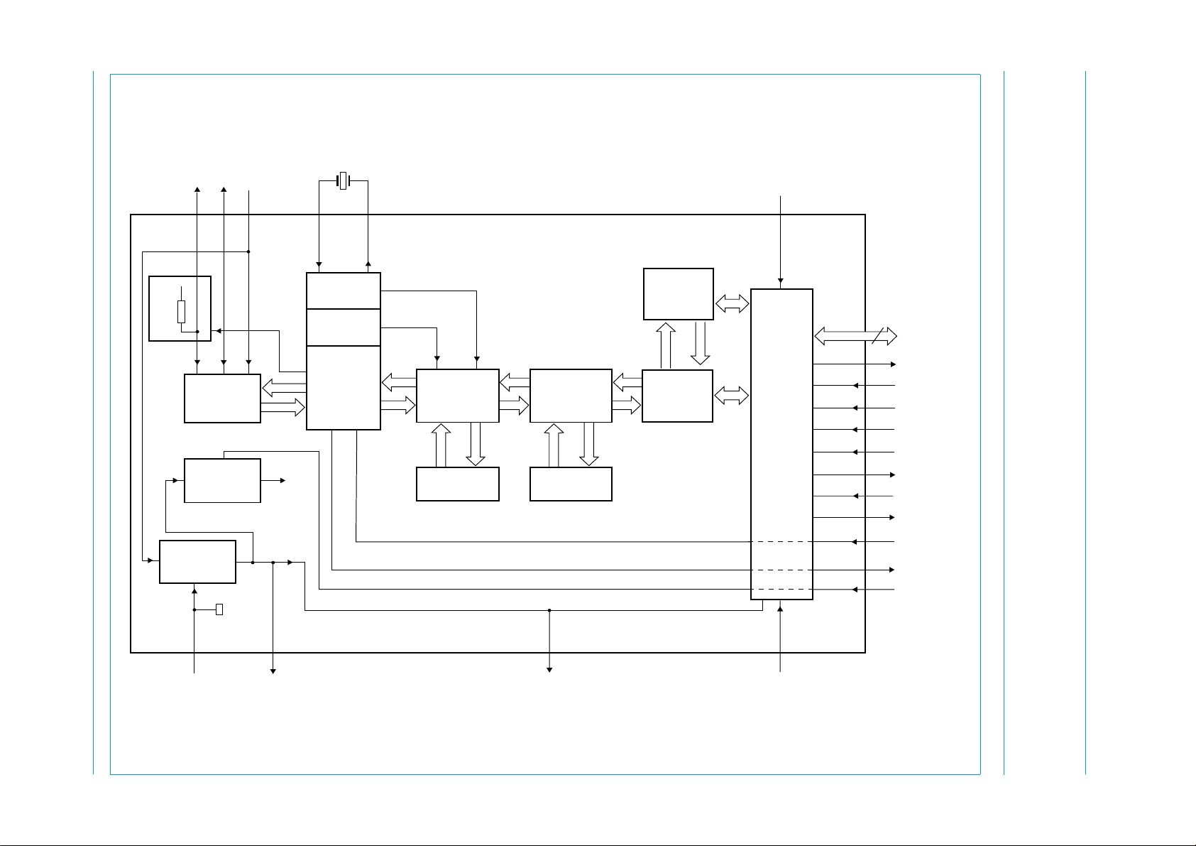
6. Block diagram
Philips Semiconductors
to and from USB
V
DM
DP
10
3.3 V
1.5
kΩ
ANALOG
POWER-ON
VOLTAGE
© Koninklijke Philips Electronics N.V. 2004. All rights reserved.
REGULATOR
Tx/Rx
RESET
BUS
9
SoftConnect
8
internal
reset
3.3 V
6 MHz
XTAL2XTAL1
67
PLL
OSCILLATOR
BIT CLOCK
RECOVERY
PHILIPS
SIE
48 MHz
12 MHz
MEMORY
MANAGEMENT
UNIT
INTEGRATED
RAM
ISP1183
CONTROLLER
HANDLER
ENDPOINT
HANDLER
MICRO
DMA
HANDLER
BUS
INTERFACE
DGND
5, 22, 25
1.65 V to
3.6 V
LEVEL
SHIFTER
PADS
19, 20,
23, 24,
26 to 29
1
2
3
4
17
13
15
14
31
32
16
to and from
microcontroller
8
DATA[7:0]
INT_N
CS_N
WR_N
RD_N
A0
VBUSDET_N
DACK
DREQ
WAKEUP
SUSPEND
RESET_N
Low-power USB interface device with DMA
11 12
AGND
Fig 1. Block diagram.
V
REG(3V3)
V
DD(I/O)
18, 30
004aaa288
ISP1183
21
V
DD
Page 5
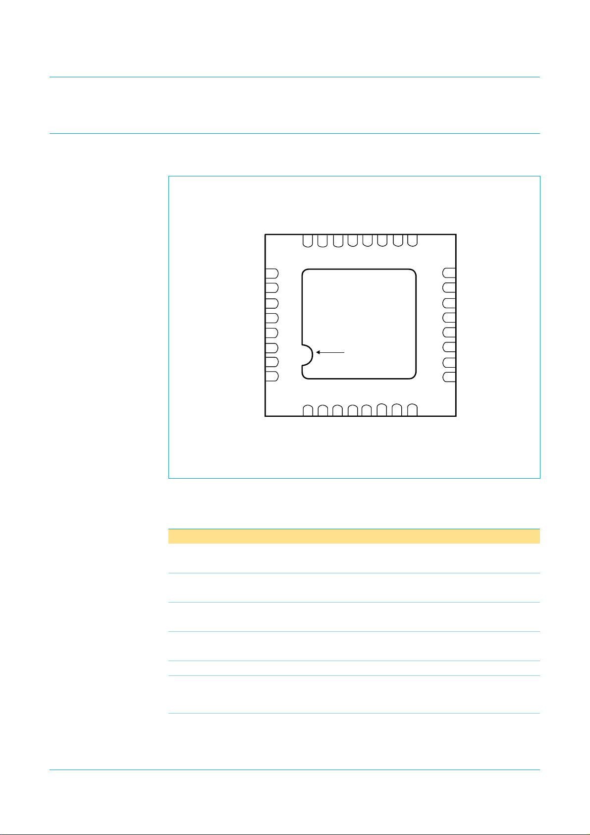
Philips Semiconductors
7. Pinning information
7.1 Pinning
ISP1183
Low-power USB interface device with DMA
REG(3V3)
AGND
DM
9
10
DP
V
VBUSDET_N
DREQ
11
14
13
12
DACK
15
RESET_N
16
V
XTAL2
XTAL1
DGND
RD_N
WR_N
CS_N
INT_N
Bottom view
BUS
8
7
6
5
4
3
2
1
GND (exposed die pad)
ISP1183BS
terminal 1
31
30
DD(I/O)
V
WAKEUP
29
DATA7
32
SUSPEND
28
DATA6
27
26
DATA5
DATA4
25
DGND
17
18
19
20
21
22
23
24
004aaa433
Fig 2. Pin configuration HVQFN32.
7.2 Pin description
Table 2: Pin description
Symbol
INT_N 1 O interrupt output; active LOW
CS_N 2 I chip select input
WR_N 3 I write strobe input
RD_N 4 I read strobe input
DGND 5 - digital ground supply
XTAL1 6 I crystal oscillator input (6 MHz); connect a fundamental
XTAL2 7 O crystal oscillator output (6 MHz); connect a fundamental
[1]
Pin Type Description
3.3 V tolerant I/O pad
3.3 V tolerant I/O pad
3.3 V tolerant I/O pad
3.3 V tolerant I/O pad
parallel-resonant crystal or an external clock source (leave
pin XTAL2 unconnected)
parallel-resonant crystal; leave this pin open when using an
external clock source on pin XTAL1
A0
V
DD(I/O)
DATA0
DATA1
V
DD
DGND
DATA2
DATA3
9397 750 11804
© Koninklijke Philips Electronics N.V. 2004. All rights reserved.
Product data Rev. 01 — 24 February 2004 5 of 62
Page 6

Philips Semiconductors
ISP1183
Low-power USB interface device with DMA
Table 2: Pin description
BUS
[1]
Pin Type Description
8IV
Symbol
V
…continued
BUS
sensing input and power supply input; see
Section 8.11
DM 9 AI/O USB D− line connection (analog)
DP 10 AI/O USB D+ line connection (analog)
AGND 11 - analog ground supply
V
REG(3V3)
12 - regulated supply voltage (3.3 V ± 10 %) from internal
regulator; used to connect a 0.1 µF decoupling capacitor
and pull-up resistor on pin DP
Remark: Cannot be used to supply external devices.
VBUSDET_N 13 O V
indicator output (active LOW); see Table 3
BUS
DREQ 14 O DMA request output (4 mA; programmable polarity, see
Table 21); signals to the DMA controller that the ISP1183
wants to start a DMA transfer
3.3 V tolerant I/O pad
DACK 15 I DMA acknowledge input (programmable polarity, see
Table 21); used by the DMA controller to signal the start of a
DMA transfer requested by the ISP1183; when not in use,
connect this pin to ground through a 10 kΩ resistor
3.3 V tolerant I/O pad
RESET_N 16 I reset input (Schmitt trigger); a LOW level produces an
asynchronous reset
3.3 V tolerant I/O pad
A0 17 I address input; selects command (A0 = HIGH) or data
(A0 = LOW)
3.3 V tolerant I/O pad
V
DD(I/O)
18 - I/O power supply; add a decoupling capacitor of 0.1 µF
(1.65 V to 3.6 V); see Section 8.11
DATA0 19 I/O data bit 0 input and output
bidirectional (4 mA), 3.3 V tolerant I/O pad
DATA1 20 I/O data bit 1 input and output
bidirectional (4 mA), 3.3 V tolerant I/O pad
V
DD
21 - 3.3 V output voltage; internally connected to the regulator
output; connect to a decoupling capacitor of 0.1 µF
DGND 22 digital ground supply
DATA2 23 I/O data bit 2 input and output
bidirectional (4 mA), 3.3 V tolerant I/O pad
DATA3 24 I/O data bit 3 input and output
bidirectional (4 mA), 3.3 V tolerant I/O pad
DGND 25 - digital ground supply
DATA4 26 I/O data bit 4 input and output
bidirectional (4 mA), 3.3 V tolerant I/O pad
DATA5 27 I/O data bit 5 input and output
bidirectional (4 mA), 3.3 V tolerant I/O pad
9397 750 11804
Product data Rev. 01 — 24 February 2004 6 of 62
© Koninklijke Philips Electronics N.V. 2004. All rights reserved.
Page 7

Philips Semiconductors
ISP1183
Low-power USB interface device with DMA
Table 2: Pin description
Symbol
[1]
Pin Type Description
…continued
DATA6 28 I/O data bit 6 input and output
bidirectional (4 mA), 3.3 V tolerant I/O pad
DATA7 29 I/O data bit 7 input and output
bidirectional (4 mA), 3.3 V tolerant I/O pad
V
DD(I/O)
30 - I/O power supply; add a decoupling capacitor of 0.1 µF
WAKEUP 31 I wake-up input (edge triggered, LOWto HIGH); generates a
remote wake-up from the suspend state; when not in use,
connect this pin to ground through a 10 kΩ resistor
3.3 V tolerant I/O pad
SUSPEND 32 O suspend state indicator output (4 mA)
3.3 V tolerant I/O pad
GND exposed
die pad
[1] Symbol names ending with underscore N (for example, NAME_N) represent active LOW signals.
- ground supply; down bonded to the exposed die pad
(heatsink); to be connected to the DGND during PCB layout
9397 750 11804
Product data Rev. 01 — 24 February 2004 7 of 62
© Koninklijke Philips Electronics N.V. 2004. All rights reserved.
Page 8

Philips Semiconductors
8. Functional description
The ISP1183 is a full-speed USB interface device with up to 14 configurable
endpoints. It has a fast general-purpose parallel interface for communication with
many types of microcontrollers and microprocessors. It supports an 8-bit data bus
with separate address and data. The block diagram is given in Figure 1.
The ISP1183 has 2462 bytes of internal FIFO memory that is shared among the
enabled USB endpoints. The type and FIFO size of each endpoint can be individually
configured, depending on the required packet size. Isochronous and bulk endpoints
are double-buffered for increased data throughput.
ISP1183
Low-power USB interface device with DMA
The ISP1183 requires two supply voltages. The core voltage is supplied from V
through an internal regulator, which transforms +5.0 V to +3.3 V when V
powered. The I/O interface voltage is supplied from V
1.65 V to 3.6 V.
The ISP1183 operates on a 6 MHz oscillator frequency.
, which can be
DD(I/O)
8.1 Analog transceiver
The transceiver is compliant with the
directly interfaces with the USB cable through external termination resistors.
Universal Serial Bus Specification Rev. 2.0
8.2 Philips SIE
The Philips Serial Interface Engine (SIE) implements the full USB protocol layer. It is
completely hardwired for speed and needs no firmware intervention. The functions of
this block include: synchronization pattern recognition, parallel-to-serial conversion,
bit (de)stuffing, CRC checkingand generation, PacketIDentifier (PID) verification and
generation, address recognition, and handshake evaluation and generation.
8.3 MMU and integrated RAM
The Memory Management Unit (MMU) and the integrated RAM provide the
conversion between the USB speed (full-speed: 12 Mbit/s bursts) and the parallel
interface to the microcontroller (maximum 11.1 Mbyte/s). This allows the
microcontroller to read and write USB packets at its own speed.
BUS
BUS
is
. It
8.4 SoftConnect
The connection to USB is accomplished by pulling pin DP (for full-speed USB
devices) HIGH through a 1.5 kΩ pull-up resistor. In the ISP1183, by default, the
1.5 kΩ pull-up resistor is integrated on-chip. The connection is established by a
command sent from the external or system microcontroller. This allows the system
microcontroller to complete its initialization sequence before deciding to establish
connection with the USB. Reinitialization of the USB connection can also be
performed without disconnecting the cable.
Remark: The tolerance of the internal resistors is 25 %. This is higher than the 5 %
tolerance specified by the USB specification. The overall voltage specification for the
connection, however, can still be met with a good margin. The decision to make use
of this feature lies with the USB equipment designer.
9397 750 11804
Product data Rev. 01 — 24 February 2004 8 of 62
© Koninklijke Philips Electronics N.V. 2004. All rights reserved.
Page 9

Philips Semiconductors
8.5 Bit clock recovery
The bit clock recovery circuit recovers the clock from the incoming USB data stream
using a 4 x oversampling principle. It can track jitter and frequency drift as specified
by the
8.6 Voltage regulator
A 5 V-to-3.3 V voltage regulator is integrated on-chip to supply the analog transceiver
and internal logic. This voltage is available at pin V
1.5 kΩ pull-up resistor on pin DP. Alternatively, the ISP1183 provides SoftConnect
technology through an integrated 1.5 kΩ pull-up resistor (see Section 8.4).
8.7 PLL clock multiplier
A 6 MHz-to-48 MHz clock multiplier Phase-Locked Loop (PLL) is integrated on-chip.
This allows for the use of a low-cost 6 MHz crystal, which also minimizes EMI. No
external components are required for the operation of the PLL.
8.8 PIO and DMA interfaces
USB Specification Rev. 2.0
ISP1183
Low-power USB interface device with DMA
.
REG(3V3)
to supply an external
A generic Parallel I/O (PIO) interface is defined for speed and ease-of-use. It also
allows direct interfacing to most microcontrollers. To a microcontroller, the ISP1183
appears as a memory device with an 8-bit data bus and a 1-bit address bus. The
ISP1183 supports nonmultiplexed address and data buses.
The ISP1183 can also be configured as a Direct Memory Access (DMA) slave device
to allow more efficient data transfer. One of the 14 endpoint FIFOs may directly
transfer data to or from the local shared memory. The DMA interface can be
independently configured from the PIO interface.
It can be directly interfaced to microprocessors or microcontrollers with I/O voltage
range as low as 1.65 V.
8.9 V
indicator
BUS
The ISP1183 indicates the availability of V
available(at pin V
(at pin V
BUS
BUS
), pin VBUSDET_N will output HIGH. Pin VBUSDET_N will change from
HIGH-to-LOW level in approximately 2.5 ms to 3.5 ms. See Section 19.
8.10 Operation modes
The ISP1183 can be operated in several operation modes as given in Table 3.
Table 3: ISP1183 operation modes
Pin name Plug-out
state
V
BUS
V
DD(I/O)
WAKEUP X X L L L
RESET_N X X L H H
INT_N H L
0VX 5V5V5V
1.8 V 0 V 1.8 V 1.8 V 1.8 V
using the V
BUS
pin. When V
BUS
), pin VBUSDET_N will output LOW. When V
Dead state Reset state Plug-in state Normal state
[1]
HH-
BUS
is not available
BUS
[2]
is
9397 750 11804
Product data Rev. 01 — 24 February 2004 9 of 62
© Koninklijke Philips Electronics N.V. 2004. All rights reserved.
Page 10
Philips Semiconductors
ISP1183
Low-power USB interface device with DMA
Table 3: ISP1183 operation modes
Pin name Plug-out
state
SUSPEND H L
VBUSDET_N H L
DATA Hi-Z L
[1] Not driven LOW.There is, however,no current flow through the pads because no I/O supply voltage is
available. Therefore, no potential will develop at the output.
[2] During the normal operation, when V
the USB bus for 3 ms or more, a suspend interrupt is generated on pin INT_N. On receiving the
suspend interrupt, the external processor issues a GOSUSP command to the device. Once the
GOSUSP command is issued by the processor, the device starts to prepare itself togo to the suspend
mode. During suspend, to reduce power consumption, the internal clocks can be shut down. Once the
deviceis completely ready to go into the suspend mode, it will assert pin SUSPEND HIGH and go into
the suspend mode. The typical time between the issuing of the GOSUSP command to the device and
the device asserting pin SUSPEND HIGH is approximately 2 ms.
[3] Independent of the external reset. Depends only on the power-on reset.
[4] On connecting the USB cable (V
approximately 2.5 ms to 3.5 ms.
8.11 Power supply
The ISP1183 is poweredfrom a single supply voltage, rangingfrom 4.0 V to 5.5 V. An
integrated voltage regulator provides a 3.3 V supply voltage for the internal logic and
the USB transceiver. This voltage is available at pin V
external pull-up resistor on USB connection pin DP. See Figure 3.
…continued
Dead state Reset state Plug-in state Normal state
[1]
[1]
[1]
BUS
), pin VBUSDET_N will change from HIGH level to LOW level in
BUS
LLL
[3]
L
H -> L
[4]
L
Hi-Z Hi-Z -
is available, pin SUSPEND is LOW. If there is no activity on
REG(3V3)
for connecting an
The ISP1183 can also be operated from a 3.0 V to 3.6 V supply, as shown in
Figure 4. In this case, the internal voltage regulator is disabled and pin V
must be connected to V
V
BUS
8
V
REG(3V3)
12
V
DD(I/O)
ISP1183
V
DD
21
18
30
004aaa295
V
DD(I/O)
1.65 V to 3.6 V
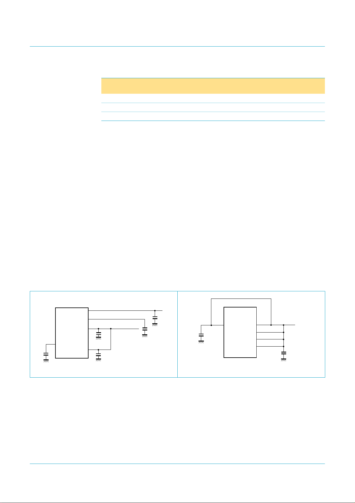
Fig 3. ISP1183 with a 4.0 V to 5.5 V supply. Fig 4. ISP1183 with a 3.0 V to 3.6 V supply.
4.0 V to 5.5 V
. For details, see Section 19.
BUS
V
DD
21
ISP1183
004aaa296
8
12
18
30
V
BUS
V
REG(3V3)
V
DD(I/O)
V
DD(I/O)
3.0 V to 3.6 V
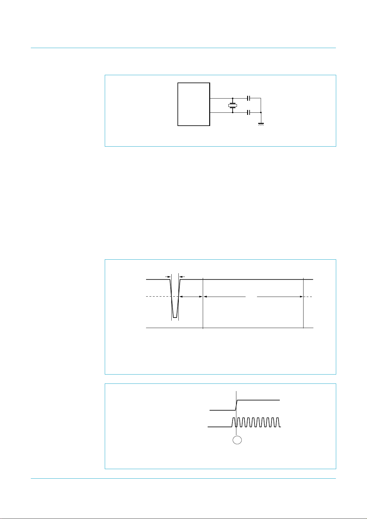
8.12 Crystal oscillator
The ISP1183 has a crystal oscillator designed for a 6 MHz parallel-resonant crystal
(fundamental). A typical circuit is shown in Figure 5. Alternatively, an external clock
signal of 6 MHz can be applied to input XTAL1, while leaving output XTAL2 open.
REG(3V3)
9397 750 11804
Product data Rev. 01 — 24 February 2004 10 of 62
© Koninklijke Philips Electronics N.V. 2004. All rights reserved.
Page 11
Philips Semiconductors
ISP1183
Low-power USB interface device with DMA
Fig 5. Typical oscillator circuit.
The 6 MHz oscillator frequency is multiplied to 48 MHz by an internal PLL.
In the suspend state, the crystal oscillator and the PLL are switched off to save
power. The oscillator operation is controlled by using bit CLKRUN in the Hardware
Configuration register. CLKRUN switches the oscillator on and off.
8.13 Power-on reset
The ISP1183 has an internal power-on reset (POR) circuit. The clock signal normally
requires 3 ms to 4 ms to stabilize.
The triggering voltage of the POR circuit is 0.5 V nominal. A POR is automatically
generated when V
50 µs.
V
DD(I/O)
0.5 V
XTAL2
6
ISP1183
004aaa294
goes below the trigger voltage for a duration longer than
DD(I/O)
POR
≤ 350 µs
7
XTAL1
18 pF
6 MHz
18 pF
2 ms
0 V
t1: clock is running
t2: registers are accessible
t
1
t
2
004aaa390
Fig 6. POR timing.
POR
EXTERNAL CLOCK
004aaa365
A
Stable external clock available at A.
Fig 7. Clock with respect to the external POR.
9397 750 11804
Product data Rev. 01 — 24 February 2004 11 of 62
© Koninklijke Philips Electronics N.V. 2004. All rights reserved.
Page 12
Philips Semiconductors
A hardware reset disables all USB endpoints and clears all Endpoint Configuration
registers (ECRs), except for the control endpoint that is fixed and always enabled.
Section 10.3 explains how to (re)initialize endpoints.
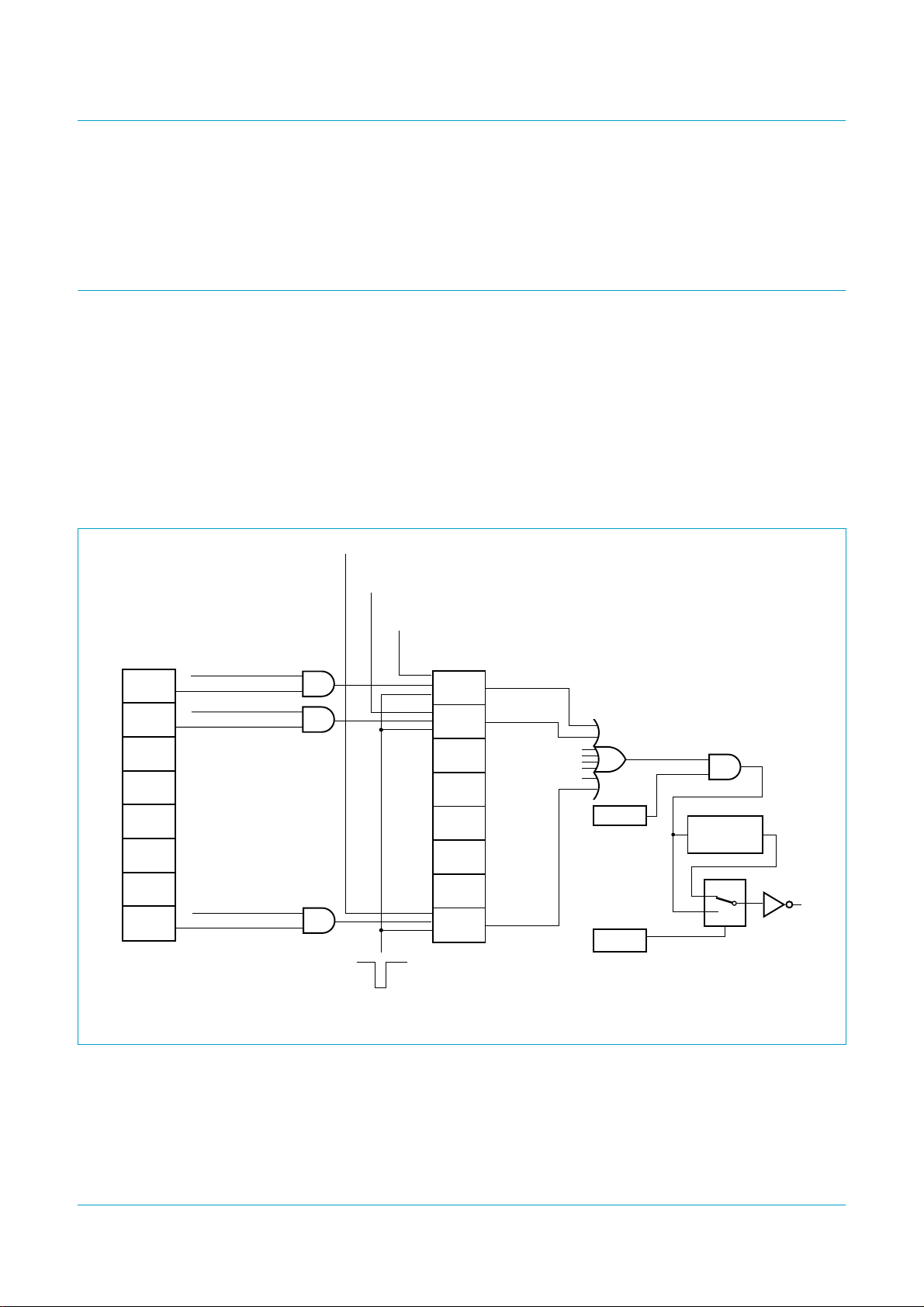
9. Interrupts
Figure 8 shows the interrupt logic of the ISP1183. Each of the indicated USB events
is logged in a status bit of the Interrupt register. Corresponding bits in the Interrupt
Enable register determine whether an event will generate an interrupt.
Interrupts can be masked globally using bit INTENA of the Mode register (see
Table 18).
The signaling mode of output INT is controlled by bit INTLVL of the Hardware
Configuration register (see Table 20). Default settings after reset is level mode. When
pulse mode is selected, a pulse of 166 ns is generated when the OR-ed combination
of all interrupt bits changes from logic 0 to logic 1.
(clear EPn interrupt; reading EPn
status register will set this signal)
ISP1183
Low-power USB interface device with DMA
reset interrupt source
IERST
IESUSP
IERESM
IESOF
interrupt enable register
IEP0IN
IEP0OUT
suspend interrupt source
IEP14
...
EPn interrupt source
Fig 8. Interrupt logic.
(clear SUSPEND interrupt; reading
interrupt register will set this signal)
(clear RESET interrupt; reading
interrupt register will set this signal)
RESET
SUSPND
.
.
.
.
.
.
.
.
.
.
.
.
RESET
.
.
.
.
.
.
.
.
.
.
.
.
RESUME
SOF
EP14
...
EP0IN
EP0OUT
interrupt register
INTENA
device mode
register
INTLVL
hardware configuration
register
PULSE
GENERATOR
1
0
004aaa255
INT
Bits SUSPND, RESET, RESUME, SP_EOT, EOT and SOF are cleared when the
Interrupt register is read. The endpoint bits (EP0OUT to EP14) are cleared when the
associated Endpoint Status register is read.
Bit BUSTATUS follows the USB bus status exactly, allowing the firmware to get the
current bus status when reading the Interrupt register.
9397 750 11804
Product data Rev. 01 — 24 February 2004 12 of 62
© Koninklijke Philips Electronics N.V. 2004. All rights reserved.
Page 13

Philips Semiconductors
SETUP and OUT token interrupts are generated after the ISP1183 has
acknowledgedthe associated data packet. In the bulk transfer mode, the ISP1183 will
issue interrupts for every ACK received for an OUT token or transmitted for an IN
token.
In the isochronous mode, an interrupt is issued on each packet transaction. The
firmware is responsible for timing synchronization with the host. This can be done
using the Pseudo Start-Of-Frame (PSOF) interrupt, enabled using bit IEPSOF in the
Interrupt Enable register. If a Start-Of-Frame is lost, PSOF interrupts are generated
every1 ms. This allowsthe firmware to keep data transfersynchronized with thehost.
After three missed SOF events, the ISP1183 will enter the suspend state.
An alternative way of handling the isochronous data transfer is to enable both the
SOF and PSOF interrupts and disable the interrupt for each isochronous endpoint.
ISP1183
Low-power USB interface device with DMA
9397 750 11804
Product data Rev. 01 — 24 February 2004 13 of 62
© Koninklijke Philips Electronics N.V. 2004. All rights reserved.
Page 14

Philips Semiconductors
10. Endpoint description
Each USB device is logically composed of several independent endpoints. An
endpoint acts as a terminus of a communication flow between the host and the
device. At design time, each endpoint is assigned a unique number (endpoint
identifier, see Table 4). The combination of the device address (given by the host
during enumeration), the endpoint number, and the transfer direction allows each
endpoint to be uniquely referenced.
The ISP1183 has 16 endpoints: endpoint 0 (control IN and OUT) plus 14 configurable
endpoints, which can be individually defined as interrupt, bulk or isochronous—IN or
OUT. Each enabled endpoint has an associated FIFO, which can be accessed either
using the parallel I/O interface or DMA.
10.1 Endpoint access
Table 4 lists the endpoint access modes and programmability. All endpoints support
I/O mode access. Endpoints 1 to 14 also support DMA access. FIFO DMA access is
selected and enabled through bits EPDIX[3:0] and DMAEN of the DMA Configuration
register. A detailed description of the DMA operation is given in Section 11.
ISP1183
Low-power USB interface device with DMA
Table 4: Endpoint access and programmability
Endpoint
identifier
0 64 (fixed) no yes no control OUT
0 64 (fixed) no yes no control IN
1 to 14 programmable supported supported supported programmable
[1] The total amount of FIFO storage allocated to enabled endpoints must not exceed 2462 bytes.
[2] IN: input for the USB host (ISP1183 transmits); OUT: output from the USB host (ISP1183 receives). The data flow direction is
determined by bit EPDIR in the Endpoint Configuration register.
FIFO size (bytes)
[1]
Double buffering I/O mode
access
DMA mode
access
Endpoint type
[2]
[2]
10.2 Endpoint FIFO size
The FIFO size determines the maximum packet size that the hardware can support
for a given endpoint. Only enabled endpoints are allocated space in the shared FIFO
storage, disabled endpoints have zero bytes. Table 5 lists programmable FIFO sizes.
The following bits in the Endpoint Configuration register (ECR) affect FIFO allocation:
• Endpoint enable bit (FIFOEN)
• Size bits of an enabled endpoint (FFOSZ[3:0])
• Isochronous bit of an enabled endpoint (FFOISO).
Remark: Register changes that affect the allocation of the shared FIFO storage
among endpoints must not be made while valid data is present in any FIFO of the
enabled endpoints. Such changes will render all FIFO contents undefined.
9397 750 11804
Product data Rev. 01 — 24 February 2004 14 of 62
© Koninklijke Philips Electronics N.V. 2004. All rights reserved.
Page 15

Philips Semiconductors
Table 5: Programmable FIFO size
FFOSZ[3:0] Nonisochronous Isochronous
0000 8 bytes 16 bytes
0001 16 bytes 32 bytes
0010 32 bytes 48 bytes
0011 64 bytes 64 bytes
0100 reserved 96 bytes
0101 reserved 128 bytes
0110 reserved 160 bytes
0111 reserved 192 bytes
1000 reserved 256 bytes
1001 reserved 320 bytes
1010 reserved 384 bytes
1011 reserved 512 bytes
1100 reserved 640 bytes
1101 reserved 768 bytes
1110 reserved 896 bytes
1111 reserved 1023 bytes
ISP1183
Low-power USB interface device with DMA
Each programmable FIFO can be independently configured through its ECR. The
total physical size of all enabled endpoints (IN plus OUT), however, must not exceed
2462 bytes.
Table 6 shows anexample of a configurationfitting in the maximum available space of
2462 bytes. The total number of logical bytes in the example is 1311. The physical
storage capacity used for double buffering is managed by the device hardware and is
transparent to the user.
Table 6: Memory configuration example
Physical size
(bytes)
64 64 control IN (64-byte fixed)
64 64 control OUT (64-byte fixed)
2046 1023 double-buffered 1023-byte isochronous endpoint
16 16 16-byte interrupt OUT
16 16 16-byte interrupt IN
128 64 double-buffered 64-byte bulk OUT
128 64 double-buffered 64-byte bulk IN
Logical size
(bytes)
Endpoint description
9397 750 11804
Product data Rev. 01 — 24 February 2004 15 of 62
© Koninklijke Philips Electronics N.V. 2004. All rights reserved.
Page 16

Philips Semiconductors
10.3 Endpoint initialization
In response to the standard USB request Set Interface, the firmware mustprogram all
16 ECRs of the ISP1183 in sequence (see Table 4), whether the endpoints are
enabled or not. The hardware will then automatically allocate FIFO storage space.
If all endpoints have been successfully configured, thefirmware mustreturn an empty
packet to the control IN endpoint to acknowledge success to the host. If there are
errors in the endpoint configuration, the firmware must stall the control IN endpoint.
When reset by hardware or through the USB bus, the ISP1183 disables all endpoints
and clears all ECRs, except for the control endpoint, which is fixed and always
enabled.
Endpoint initialization can be done at any time. It is, however, valid only after
enumeration.
10.4 Endpoint I/O mode access
When an endpoint event occurs (a packet is transmitted or received), the associated
endpoint interrupt bits (EPn) of the Interrupt register (IR) are set by the SIE. The
firmware then responds to the interrupt and selects the endpoint for processing.
ISP1183
Low-power USB interface device with DMA
The endpoint interrupt bit is cleared when the Endpoint Status register (ESR) is read.
The ESR also contains information on the status of the endpoint buffer.
For an OUT (= receive) endpoint, the packet length and the packet data can be read
from the ISP1183 by using the Read Buffer command. When the whole packet is
read, the firmware sends a Clear Buffer command to enable the reception of new
packets.
For an IN (= transmit) endpoint, the packet length and data to be sent can be written
to the ISP1183 by using the Write Buffer command. When the whole packet is written
to the buffer, the firmware sends a Validate Buffer command to enable data
transmission to the host.
10.5 Special actions on control endpoints
Control endpoints require special firmware actions. The arrival of a SETUP packet
flushes the IN buffer and disables the Validate Buffer and Clear Buffer commands for
the control IN and OUT endpoints. The microcontroller needs to re-enable these
commands by sending an Acknowledge Setup command to both control endpoints.
This ensures that the last SETUP packet stays in the buffer and that no packets can
be sent back to the host until the microcontroller has explicitly acknowledged that it
has seen the SETUP packet.
9397 750 11804
Product data Rev. 01 — 24 February 2004 16 of 62
© Koninklijke Philips Electronics N.V. 2004. All rights reserved.
Page 17

Philips Semiconductors
11. DMA transfer
Direct Memory Access (DMA) is a method to transfer data from one location to
another in a computer system, without intervention of the central processor unit
(CPU). Many implementations of DMA exist. The ISP1183 supports two methods:
ISP1183
Low-power USB interface device with DMA
• 8237 compatible mode: based on the DMA subsystem of the IBM
computers (PC, AT and all its successors and clones); this architecture uses the
Intel® 8237 DMA controller and has separate address spaces for memory and I/O
• DACK-only mode: based on the DMA implementation in some embedded RISC
processors, which has a single address space for both memory and I/O.
The ISP1183 supports DMA transfer for all 14 configurable endpoints (see Table 4).
Only one endpoint can be selected at a time for DMA transfer. The DMA operation of
the ISP1183 can be interleaved with normal I/O mode access to other endpoints.
The following features are supported:
• Single-cycle or burst transfers (up to 16 bytes per cycle)
• Programmable transfer direction (read or write)
• Programmable signal levels on pins DREQ and DACK.
11.1 Selecting an endpoint for DMA transfer
The target endpoint for DMA access is selected through bits EPDIX[3:0] in the DMA
Configuration register, see Table 7. The transfer direction (read or write) is
automatically set bybit EPDIR in the associated ECR, to match the selected endpoint
type (OUT endpoint: read; IN endpoint: write).
Asserting input DACK automatically selects the endpoint specified in the DMA
Configuration register, regardless of the current endpoint used for I/O mode access.
®
personal
Table 7: Endpoint selection for DMA transfer
Endpoint
identifier
1 0010 OUT: read IN: write
2 0011 OUT: read IN: write
3 0100 OUT: read IN: write
4 0101 OUT: read IN: write
5 0110 OUT: read IN: write
6 0111 OUT: read IN: write
7 1000 OUT: read IN: write
8 1001 OUT: read IN: write
9 1010 OUT: read IN: write
10 1011 OUT: read IN: write
11 1100 OUT: read IN: write
12 1101 OUT: read IN: write
13 1110 OUT: read IN: write
14 1111 OUT: read IN: write
9397 750 11804
Product data Rev. 01 — 24 February 2004 17 of 62
EPDIX[3:0] Transfer direction
EPDIR = 0 EPDIR = 1
© Koninklijke Philips Electronics N.V. 2004. All rights reserved.
Page 18

Philips Semiconductors
11.2 8237 compatible mode
The 8237 compatible DMA mode is selected by clearing bit DAKOLY in the Hardware
Configuration register (see Table 20). The pin functions for this mode are shown in
Table 8.
Table 8: 8237 compatible mode: pin functions
Symbol Description I/O Function
DREQ DMA request O ISP1183 requests a DMA transfer
DACK DMA acknowledge I DMA controller confirms the transfer
RD_N read strobe I instructs the ISP1183 to put data on the bus
WR_N write strobe I instructs the ISP1183 to get data from the bus
The DMA subsystem of an IBM-compatible PC is based on the Intel 8237 DMA
controller. It operates as a ‘fly-by’ DMA controller: the data is not stored in the DMA
controller, but it is transferred between an I/O port and a memory address. A typical
example of the ISP1183 in the 8237-compatible DMA mode is given in Figure 9.
The 8237 has two control signals for each DMA channel: DREQ (DMA request) and
DACK_N (DMA acknowledge). General control signals are HRQ (hold request) and
HLDA (hold acknowledge). The bus operation is controlled using MEMR_N (memory
read), MEMW_N (memory write), IOR_N (I/O read) and IOW_N (I/O write).
ISP1183
Low-power USB interface device with DMA
DATA[7:0]
ISP1183
RAM
DREQ
DACK
RD_N
WR_N
MEMR_N
MEMW_N
DMA
CONTROLLER
8237
DREQ HRQ
DACK_N
IOR_N
IOW_N
Fig 9. ISP1183 in the 8237-compatible DMA mode.
HLDA
CPU
HRQ
HLDA
004aaa291
9397 750 11804
Product data Rev. 01 — 24 February 2004 18 of 62
© Koninklijke Philips Electronics N.V. 2004. All rights reserved.
Page 19

Philips Semiconductors
The following example shows the steps that occur in a typical DMA transfer:
1. The ISP1183 receives a data packet in one of its endpoint FIFOs; the packet
2. The ISP1183 asserts the DREQ signal requesting the 8237 for a DMA transfer.
3. The 8237 asks the CPU to release the bus by asserting the HRQ signal.
4. After completing the current instruction cycle, the CPU places the bus control
5. The8237 sets its address linesto 1234H and activates the MEMW_N and IOR_N
6. The8237 asserts DACK_Nto inform the ISP1183 that it will start a DMA transfer.
7. The ISP1183 places the byte or word to be transferred on the data bus lines
8. The 8237 waits one DMA clock period and then deasserts MEMW_N and
9. The ISP1183 deasserts the DREQ signal to indicate to the 8237 that DMA is no
10. The 8237 deasserts the DACK_N output indicating that the ISP1183 must stop
11. The 8237 places the bus control signals (MEMR_N, MEMW_N, IOR_N and
12. The CPU acknowledges control of the bus by deasserting HLDA. After activating
ISP1183
Low-power USB interface device with DMA
must be transferred to memory address 1234H.
signals (MEMR_N, MEMW_N, IOR_N and IOW_N) and the address lines in
three-state and asserts HLDA to inform the 8237 that it has control of the bus.
control signals.
because its RD_N signal was asserted by the 8237.
IOR_N. This latches and stores the byte or word at the desired memory location.
It also informs the ISP1183 that the data on the bus lines has been transferred.
longer needed. In the single cycle mode this is done after each byte or word, in
the burst mode following the last transferred byte or word of the DMA cycle.
placing data on the bus.
IOW_N) and the address lines in three-state and deasserts the HRQ signal,
informing the CPU that it has released the bus.
the bus control lines (MEMR_N, MEMW_N, IOR_N and IOW_N)and the address
lines, the CPU resumes the execution of instructions.
For a typical bulk transfer, the above process is repeated 64 times, once for each
byte. After each byte, the address register in the DMA controller is incremented and
the byte counter is decremented.
11.3 DACK-only mode
The DACK-only DMA mode is selected by setting bit DAKOLY in the Hardware
Configuration register (see Table 20). The pin functions for this mode are shown in
Table 9. A typical example of the ISP1183 in the DACK-only DMA mode is given in
Figure 10.
Table 9: DACK-only mode: pin functions
Symbol Description I/O Function
DREQ DMA request O ISP1183 requests a DMA transfer
DACK DMA acknowledge I DMA controller confirms the transfer;
also functions as data strobe
RD_N read strobe I not used
WR_N write strobe I not used
9397 750 11804
Product data Rev. 01 — 24 February 2004 19 of 62
© Koninklijke Philips Electronics N.V. 2004. All rights reserved.
Page 20

Philips Semiconductors
In the DACK-only mode, the ISP1183 uses the DACK signal as data strobe. Input
signals RD_N and WR_N are ignored. This mode is used in CPU systems that havea
single address space for memory and I/O access. Such systems have no separate
MEMW_N and MEMR_N signals: the RD_N and WR_N signals are also used as
memory data strobes.
ISP1183
Low-power USB interface device with DMA
ISP1183 DMA
DREQ
DACK
DATA[7:0]
Fig 10. ISP1183 in the DACK-only DMA mode.
11.4 End-Of-Transfer conditions
11.4.1 Bulk endpoints
A DMA transfer to or from a bulk endpoint can be terminated by any of the following
conditions (for bit names, refer to the DMA Configuration register in Table 32):
• The DMA transfer completes as programmed in the DMA Counter register
(CNTREN = 1)
• A short packet is received on an enabled OUT endpoint (SHORTP = 1)
• DMA operation is disabled by clearing bit DMAEN.
RAM
CONTROLLER
DREQ_N
DACK_N
RD_N
WR_N
HRQ
HLDA
CPU
HRQ
HLDA
004aaa292
DMA Counter register: An EOT from the DMA Counter register is enabledby setting
bit CNTREN in the DMA Configuration register. The ISP1183 has a 16-bit DMA
Counter register,which specifies the number of bytes to be transferred. When DMA is
enabled (DMAEN = 1), the internal DMA counter is loaded with the value from the
DMA Counter register. When the internal counter completes the transfer as
programmed in the DMA counter, an EOT condition is generated and the DMA
operation stops.
Short packet: Normally, the transfer byte count must be set though a control
endpoint before any DMA transfer occurs. When a short packet has been enabled as
EOT indicator (SHORTP = 1), the transfer size is determined by the presence of a
short packet in the data. This mechanism permits the use of a fully autonomous data
transfer protocol.
When reading from an OUT endpoint, reception of a short packet at an OUT token
will stop the DMA operation after transferring the data bytes of this packet.
9397 750 11804
Product data Rev. 01 — 24 February 2004 20 of 62
© Koninklijke Philips Electronics N.V. 2004. All rights reserved.
Page 21

Philips Semiconductors
Table 10: Summary of EOT conditions for a bulk endpoint
EOT condition OUT endpoint IN endpoint
DMA Counter register transfer completes as
Short packet short packet is received and
DMAEN bit in DMA
Configuration register
[1] The DMA transfer stops. No interrupt, however, is generated.
11.4.2 Isochronous endpoints
A DMA transfer to or from an isochronous endpoint can be terminated by any of the
following conditions (for bit names refer to the DMA Configuration register in
Table 32):
• The DMA transfer completes as programmed in the DMA Counter register
• DMA operation is disabled by clearing bit DMAEN.
(CNTREN = 1)
Low-power USB interface device with DMA
programmed in the DMA
Counter register
transferred
DMAEN = 0
[1]
ISP1183
transfer completes as
programmed in the DMA
Counter register
counter reaches zero in the
middle of the buffer
DMAEN = 0
[1]
Table 11: Recommended EOT usage for isochronous endpoints
EOT condition OUT endpoint IN endpoint
DMA Counter register zero do not use preferred
Clear DMAEN bit preferred do not use
9397 750 11804
Product data Rev. 01 — 24 February 2004 21 of 62
© Koninklijke Philips Electronics N.V. 2004. All rights reserved.
Page 22

Philips Semiconductors
12. Suspend and resume
12.1 Suspend conditions
The ISP1183 detects a USB suspend status when a constant idle state is present on
the USB bus for more than 3 ms.
The bus-powered devices that are suspended must not consume more than 500 µA
of current. This is achieved by shutting down power to system components or
supplying them with a reduced voltage.
The steps leading up to suspend status are as follows:
1. On detection of a wakeup-to-suspendtransition, the ISP1183 sets bit SUSPND in
the Interrupt register. This will generate an interrupt if bit IESUSP in the Interrupt
Enable register is set.
2. When the firmware detects a suspend condition, it must prepare all system
components for the suspend state:
a. All signals connected to the ISP1183 must enter appropriate states to meet
the power consumption requirements of the suspend state.
b. All input pins of the ISP1183 must have a CMOS LOW or HIGH level.
3. In the interrupt service routine, the firmware must check the current status of the
USB bus. When bit BUSTATUS in the Interrupt register is logic 0, the USB bus
has left the suspend mode and the process must be aborted. Otherwise, the next
step can be executed.
4. To meet the suspend current requirements for a bus-powereddevice, the internal
clocks must be switched off by clearing bit CLKRUN in the Hardware
Configuration register.
5. When the firmware has set and cleared bit GOSUSP in the Mode register, the
ISP1183 enters the suspend state. In powered-off application, the ISP1183
asserts output SUSPEND and switches off the internal clocks after 2 ms.
ISP1183
Low-power USB interface device with DMA
Figure 11 shows a typical timing diagram.
9397 750 11804
Product data Rev. 01 — 24 February 2004 22 of 62
© Koninklijke Philips Electronics N.V. 2004. All rights reserved.
Page 23

Philips Semiconductors
ISP1183
Low-power USB interface device with DMA
A
USB BUS
INT_N
GOSUSP
WAKEUP
SUSPEND
Fig 11. Suspend and resume timing.
In Figure 11:
• A: indicates the point at which the USB bus enters the idle state.
• B: indicates resume condition, which can be a 20 ms K-state on the USB bus, a
HIGH level on pin WAKEUP, or a LOW level on pin CS_N.
• C: indicates remote wake-up. The ISP1183 will drive a K-state on the USB bus for
10 ms after pin WAKEUP goes HIGH or pin CS_N goes LOW.
• D: after detecting the suspend interrupt, set and clear bit GOSUSP in the Mode
register.
> 3 ms
suspend
interrupt
> 5 ms
idle state
D
1.8 ms to 2.2 ms
resume
interrupt
B
0.5 ms to 3.5 ms
C
10 ms
K-state
004aaa359
12.1.1 Powered-off application
Figure 12 shows a typical bus-powered modem application using the ISP1183. The
SUSPEND output switchesoff power to the microcontroller and other external circuits
during the suspend state. The ISP1183 is woken up through the USB bus (global
resume) or by the ring detection circuit on the telephone line.
V
BUS
V
BUS
USB
DP
DM
ISP1183
SUSPEND
WAKEUP
Fig 12. SUSPEND and WAKEUP signals in a powered-off modem application.
9397 750 11804
Product data Rev. 01 — 24 February 2004 23 of 62
V
CC
8031
RST
RING DETECTION
© Koninklijke Philips Electronics N.V. 2004. All rights reserved.
LINE
004aaa293
Page 24

Philips Semiconductors
12.2 Resume conditions
A wake-up from the suspend state is initiated either by the USB host or by the
application:
• USB host: drives a K-state on the USB bus (global resume)
• Application: remote wake-up through a HIGH level on input WAKEUP or a LOW
The steps of a wake-up sequence are as follows:
1. The internal oscillator and the PLL multiplier are re-enabled. When stabilized, the
2. The SUSPEND output is deasserted, and bit RESUME in the Interrupt register is
3. Maximum 15 ms after starting the wake-up sequence, the ISP1183 resumes its
4. In case of a remote wake-up, the ISP1183 drives a K-state on the USB bus for
5. Following the deassertion of output SUSPEND, the application restores itself and
6. After wake-up,the internal registers of the ISP1183 are write-protected to prevent
ISP1183
Low-power USB interface device with DMA
level on input CS_N (if enabled using bit WKUPCS in the Hardware Configuration
register). Wake-up on CS_N will work only if V
clock signals are routed to all internal circuits of the ISP1183.
set. This will generate an interrupt if bit IERESUME in the Interrupt Enable
register is set.
normal functionality.
10 ms.
other system components to the normal operating mode.
corruption by inadvertent writing during power-up of external components. The
firmware must send an Unlock Device command to the ISP1183 to restore its full
functionality. For more details, see Section 13.4.2.
is present.
BUS
12.3 Control bits in suspend and resume
Table 12: Summary of control bits
Register Bit Function
Interrupt SUSPND a transition from awake to the suspend state was detected
BUSTATUS monitors USB bus status (logic 1 = suspend); used when
interrupt is serviced
RESUME a transition from suspend to the resume state was detected
Interrupt Enable IESUSP enables output INT to signal the suspend state
IERESUME enables output INT to signal the resume state
Mode SOFTCT enables SoftConnect pull-up resistor to USB bus
GOSUSP a HIGH-to-LOW transition enables the suspend state
Hardware
Configuration
Unlock all sending data AA37H unlocks the internal registers for
9397 750 11804
Product data Rev. 01 — 24 February 2004 24 of 62
EXTPUL selects internal (SoftConnect) or external pull-up resistor
WKUPCS enables wake-up on LOW level of input CS_N
PWROFF selects powered-off mode during the suspend state
writing after a resume
© Koninklijke Philips Electronics N.V. 2004. All rights reserved.
Page 25

Philips Semiconductors
ISP1183
Low-power USB interface device with DMA
13. Commands and registers
The functions and registers of the ISP1183 are accessed using commands, which
consist of a command code followed by optional data bytes (read or write action). An
overview of the available commands and registers is given in Table 13.
A complete access consists of two phases:
1. Command phase: when address pin A0 = HIGH, the ISP1183 interprets the
data on the lower byte of the bus pins D[7:0] as a command code. Commands
without a data phase are immediately executed.
2. Data phase (optional): when address pin A0 = LOW, the ISP1183 transfers the
data on the bus to or from a register or endpoint FIFO. Multibyte registers are
accessed least significant byte or word first.
Table 13: Command and register summary
Name Destination Code
(hex)
Initialization commands
Write Control OUT
Configuration
Write Control IN Configuration Endpoint Configuration
Write Endpoint n Configuration
(n = 1 to 14)
Read Control OUT
Configuration
Read Control IN Configuration Endpoint Configuration
Read Endpoint n Configuration
(n = 1 to 14)
Write or read Device Address Address register B6/B7 write or read 1 byte Section 13.1.2 on page 28
Write or read Mode register Mode register B8/B9 write or read 1 byte Section 13.1.3 on page 29
Write or read Hardware
Configuration
Write or read Interrupt Enable
register
Reset Device resets all registers F6 - Section 13.1.6 on page 32
Endpoint Configuration
register endpoint 0 OUT
register endpoint 0 IN
Endpoint Configuration
register endpoints 1 to 14
Endpoint Configuration
register endpoint 0 OUT
register endpoint 0 IN
Endpoint Configuration
register endpoints 1 to 14
Hardware Configuration
register
Interrupt Enable register C2/C3 write or read 4 bytes Section 13.1.5 on page 30
20 write 1 byte Section 13.1.1 on page 27
21 write 1 byte
22 to 2F write 1 byte
30 read 1 byte
31 read 1 byte
32 to 3F read 1 byte
BA/BB write or read 2 bytes Section 13.1.4 on page 29
Transaction Reference
9397 750 11804
Product data Rev. 01 — 24 February 2004 25 of 62
© Koninklijke Philips Electronics N.V. 2004. All rights reserved.
Page 26

Philips Semiconductors
ISP1183
Low-power USB interface device with DMA
Table 13: Command and register summary
Name Destination Code
…continued
Transaction Reference
(hex)
Data flow commands
Write Control OUT Buffer illegal: endpoint is
(00) - Section 13.2.1 on page 32
read-only
Write Control IN Buffer FIFO endpoint 0 IN 01 N ≤ 64 bytes
Write Endpoint n Buffer
(n = 1 to 14)
FIFO endpoints 1 to 14
(IN endpoints only)
02 to 0F isochronous:
N ≤ 1023 bytes
interrupt or bulk:
N ≤ 64 bytes
Read Control OUT Buffer FIFO endpoint 0 OUT 10 N ≤ 64 bytes
Read Control IN Buffer illegal: endpoint is
(11) -
write-only
Read Endpoint n Buffer
(n = 1 to 14)
FIFO endpoints 1 to 14
(OUTendpoints only)
12 to 1F isochronous:
N ≤ 1023 bytes
interrupt or bulk:
N ≤ 64 bytes
Stall Control OUT Endpoint Endpoint 0 OUT 40 - Section 13.2.3 on page 34
Stall Control IN Endpoint Endpoint 0 IN 41 Stall Endpoint n (n = 1 to 14) Endpoints 1 to 14 42 to 4F Read Control OUT Status Endpoint Status register
50 read 1 byte Section 13.2.2 on page 33
endpoint 0 OUT
Read Control IN Status Endpoint Status register
51 read 1 byte
endpoint 0 IN
Read Endpoint n Status
(n = 1 to 14)
Validate Control OUT Buffer illegal: IN endpoints
Endpoint Status register n
endpoints 1 to 14
[1]
only
52 to 5F read 1 byte
(60) - Section 13.2.4 on page 34
Validate Control IN Buffer FIFO endpoint 0 IN 61 Validate Endpoint n Buffer
(n = 1 to 14)
FIFO endpoints 1 to 14
(IN endpoints only)
[1]
62 to 6F -
Clear Control OUT Buffer FIFO endpoint 0 OUT 70 - Section 13.2.5 on page 35
Clear Control IN Buffer illegal
Clear Endpoint n Buffer
(n = 1 to 14)
[2]
FIFO endpoints 1 to 14
(OUTendpoints only)
(71) 72 to 7F -
[2]
Unstall Control OUT Endpoint Endpoint 0 OUT 80 - Section 13.2.3 on page 34
Unstall Control IN Endpoint Endpoint 0 IN 81 Unstall Endpoint n (n = 1 to 14) Endpoints 1 to 14 82 to 8F Check Control OUT Status
Endpoint Status Image
D0 read 1 byte Section 13.2.6 on page 35
[3]
register endpoint 0 OUT
Check Control IN Status
[3]
Endpoint Status Image
D1 read 1 byte
register endpoint 0 IN
Check Endpoint n Status
(n = 1 to 14)
[3]
Endpoint Status Image
register n
D2 to DF read 1 byte
endpoints 1 to 14
Acknowledge Setup Endpoint 0 IN and OUT F4 - Section 13.2.7 on page 36
9397 750 11804
Product data Rev. 01 — 24 February 2004 26 of 62
© Koninklijke Philips Electronics N.V. 2004. All rights reserved.
Page 27

Philips Semiconductors
ISP1183
Low-power USB interface device with DMA
Table 13: Command and register summary
Name Destination Code
DMA commands
Write or read DMAFunction and
Scratch register
Write or read DMA
Configuration
Write or read DMA Counter DMA Counter register F2/F3 write or read 2 bytes Section 13.3.3 on page 38
General commands
Read Control OUT Error Code Error Code register
Read Control IN Error Code Error Code register
Read Endpoint n Error Code
(n = 1 to 14)
Unlock Device all registers with write
Read Frame Number Frame Number register B4 read 1 or 2 bytes Section 13.4.3 on page 40
Read Chip ID Chip ID register B5 read 2 bytes Section 13.4.4 on page 41
Read Interrupt register Interrupt register C0 read 4 bytes Section13.4.5 on page 41
DMA Function and
Scratch register
DMA Configuration
register
endpoint 0 OUT
endpoint 0 IN
Error Code register
endpoints 1 to 14
access
…continued
Transaction Reference
(hex)
B2/B3 write or read 2 bytes Section 13.3.1 on page 36
F0/F1 write or read 2 bytes Section 13.3.2 on page 37
A0 read 1 byte Section 13.4.1 on page 38
A1 read 1 byte
A2 to AF read 1 byte
B0 write 2 bytes Section 13.4.2 on page 39
[1] Validating an OUT endpoint buffer causes unpredictable behavior of the ISP1183.
[2] Clearing an IN endpoint buffer causes unpredictable behavior of the ISP1183.
[3] Reads a copy of the Status register: executing this command does not clear any status bits or interrupt bits.
13.1 Initialization commands
Initialization commands are used during the enumeration process of the USB
network. These commands are used to configure and enable the embedded
endpoints. They also set the USB assigned address of the ISP1183 and perform
device reset.
13.1.1 Endpoint Configuration register (R/W: 30H–3FH/20H–2FH)
This command accesses the Endpoint Configuration register (ECR) of the target
endpoint. It defines the endpoint type (isochronous or bulk/interrupt), direction
(OUT/IN), FIFO size and buffering scheme. It also enables the endpoint FIFO. The
register bit allocation is shown in Table 14. A bus reset will disable all endpoints.
The allocation of FIFO memory takes place only after all 16 endpoints have been
configured in sequence (from endpoint 0 OUT to endpoint 14). Although the control
endpoints have fixed configurations, they must be included in the initialization
sequence and configured with their default values (see Table 4). Automatic FIFO
allocation starts when endpoint 14 is configured.
Remark: If any change is made to an endpoint configuration that affects the allocated
memory (size, enable/disable), the FIFO memory contents of all endpoints become
invalid. Therefore, all valid data must be removed from enabled endpoints before
changing the configuration.
Code (hex): 20 to 2F — write (control OUT, control IN, endpoints 1 to 14)
9397 750 11804
Product data Rev. 01 — 24 February 2004 27 of 62
© Koninklijke Philips Electronics N.V. 2004. All rights reserved.
Page 28

Philips Semiconductors
ISP1183
Low-power USB interface device with DMA
Code (hex): 30 to 3F — read (control OUT, control IN, endpoints 1 to 14)
Transaction — write or read 1 byte
Table 14: Endpoint Configuration register: bit allocation
Bit 7 6 5 4 3 2 1 0
Symbol FIFOEN EPDIR DBLBUF FFOISO FFOSZ[3:0]
[1][2]
Reset
Access R/W R/W R/W R/W R/W R/W R/W R/W
[1] The reset value of the control OUT endpoint is fixed as 0x83 for the Endpoint Configuration register.
[2] The reset value of the control IN endpoint is fixed as 0xC3 for the Endpoint Configuration register.
00000000
Table 15: Endpoint Configuration register: bit description
Bit Symbol Description
7 FIFOEN Logic 1 indicates an enabled FIFO with allocated memory.
Logic 0 indicates a disabled FIFO (no bytes allocated).
6 EPDIR This bit defines the endpoint direction (0 = OUT, 1 = IN). It also
determines the DMA transfer direction (0 = read, 1 = write).
5 DBLBUF Logic 1 indicates that this endpoint has double buffering.
4 FFOISO Logic 1 indicates an isochronous endpoint. Logic 0 indicates a
bulk or interrupt endpoint.
3 to 0 FFOSZ[3:0] This field specifies the FIFO size according to Table 5.
13.1.2 Address register (R/W: B7H/B6H)
This command sets the USB assigned address in the Address register and enables
the USB device. The Address register bit allocation is shown in Table 16.
A USB bus reset sets the device address to 00H (internally) and enables the device.
The value of the Address register (accessible by the microcontroller) is not altered by
the bus reset. In response to the standard USB request (Set Address), the firmware
must issue a Write Device Address command, followed by sending an empty packet
to the host. The new device address is activated when the host acknowledges the
empty packet.
Code (hex): B6/B7 — write or read Address register
Transaction — write or read 1 byte
Table 16: Address register: bit allocation
Bit 7 6 5 4 3 2 1 0
Symbol DEVEN DEVADR[6:0]
Reset 00000000
Access R/W R/W R/W R/W R/W R/W R/W R/W
Table 17: Address register: bit description
Bit Symbol Description
7 DEVEN Logic 1 enables the device.
6 to 0 DEVADR[6:0] This field specifies the USB device address.
9397 750 11804
Product data Rev. 01 — 24 February 2004 28 of 62
© Koninklijke Philips Electronics N.V. 2004. All rights reserved.
Page 29

Philips Semiconductors
ISP1183
Low-power USB interface device with DMA
13.1.3 Mode register (R/W: B9H/B8H)
This command accesses the ISP1183 Mode register, which consists of 1 byte (bit
allocation: see Table 18). In the 16-bit bus mode, the upper byte is ignored.
The Mode register controls the DMA bus width, resume and suspend modes,
interrupt activity and SoftConnect operation. It can be used to enable debug mode, in
which all errors and Not Acknowledge (NAK) conditions will generate an interrupt.
Code (hex): B8/B9 — write or read Mode register
Transaction — write or read 1 byte
Table 18: Mode register: bit allocation
Bit 7 6 5 4 3 2 1 0
Symbol reserved reserved GOSUSP reserved INTENA DBGMOD reserved SOFTCT
Reset 0
Access R/W R/W R/W R/W R/W R/W R/W R/W
[1] Unchanged by a bus reset.
[1]
0000
[1]
[1]
0
[1]
0
[1]
0
Table 19: Mode register: bit description
Bit Symbol Description
7 reserved This bit should be always written as logic 0.
6 - reserved
5 GOSUSP Writing logic 1 followed by logic 0 will activate the suspend mode.
4 - reserved
3 INTENA Logic 1 enables all interrupts. Bus reset value: unchanged.
2 DBGMOD Logic 1 enables the debug mode, in which all NAKs and errors
will generate an interrupt. Logic 0 selects normal operation, in
which interrupts are generated on every ACK (bulk endpoints) or
after every data transfer (isochronous endpoints). Bus reset
value: unchanged.
1 - reserved
0 SOFTCT Logic 1 enables SoftConnect (see Section 8.4). This bit is ignored
if EXTPUL = 1 in the Hardware Configuration register (see
Table 20). Bus reset value: unchanged.
13.1.4 Hardware Configuration register (R/W: BBH/BAH)
This command accesses the Hardware Configuration register that consists of
2 bytes. The first (lower) byte contains the device configuration and control values,
the second (upper) byte holds the clock control bits and the clock division factor. The
bit allocation is given in Table 20. A bus reset will not change any of the programmed
bit values.
The Hardware Configuration register controls the connection to the USB bus, clock
activity and power supply during the suspend state, output clock frequency, DMA
operating mode and pin configurations (polarity, signaling mode).
Code (hex): BA/BB — write or read Hardware Configuration register
Transaction — write or read 2 bytes
9397 750 11804
Product data Rev. 01 — 24 February 2004 29 of 62
© Koninklijke Philips Electronics N.V. 2004. All rights reserved.
Page 30

Philips Semiconductors
ISP1183
Low-power USB interface device with DMA
Table 20: Hardware Configuration register: bit allocation
Bit 15 14 13 12 11 10 9 8
Symbol reserved EXTPUL reserved CLKRUN reserved
Reset 00100011
Access R/W R/W R/W R/W R/W R/W R/W R/W
Bit 7 6 5 4 3 2 1 0
Symbol DAKOLY DRQPOL DAKPOL reserved WKUPCS reserved INTLVL reserved
Reset 01000100
Access R/W R/W R/W R/W R/W R/W R/W R/W
Table 21: Hardware Configuration register: bit description
Bit Symbol Description
15 - reserved
14 EXTPUL Logic 1 indicates that an external 1.5 kΩ pull-up resistor is used
on pin DP and that SoftConnect is not used. Bus reset value:
unchanged.
13 - reserved
12 CLKRUN Logic 1 indicates that the internal clocks are always running,
even during the suspend state. Logic 0 switches off the internal
oscillator and PLL, when they are not needed. During the
suspend state,this bit must be made logic 0 to meet the suspend
current requirements. The clock is stopped after a delay of
approximately 2 ms, following the setting of bit GOSUSP in the
Mode register. Bus reset value: unchanged.
11 to 8 - reserved
7 DAKOLY Logic 1 selects the DACK-only DMA mode. Logic 0 selects the
8237 compatible DMA mode. Bus reset value: unchanged.
6 DRQPOL Selects DREQ signal polarity (0 = active LOW, 1 = active HIGH).
Bus reset value: unchanged.
5 DAKPOL Selects DACK signal polarity (0 = active LOW, 1 = active HIGH).
Bus reset value: unchanged.
4 reserved This bit should be always written as logic 0.
3 WKUPCS Logic 1 enables remote wake-up through a LOW level on input
CS_N (For wake-up on CS_N to work, V
Bus reset value: unchanged.
2 - reserved
1 INTLVL Selects the interrupt signaling mode on output INT (0 = level,
1 = pulsed). In the pulsed mode, an interrupt produces 166 ns
pulse. For details, see Section 12. Bus reset value: unchanged.
0 reserved This bit should be always written as logic 0.
must be present).
BUS
13.1.5 Interrupt Enable register (R/W: C3H/C2H)
This command individually enables or disables interrupts from all endpoints, as well
as interrupts caused by events on the USB bus (SOF, SOF lost, EOT, suspend,
resume, reset). A bus reset will not change any of the programmed bit values.
The command accesses the Interrupt Enable register that consists of 4 bytes. The bit
allocation is given in Table 22.
9397 750 11804
Product data Rev. 01 — 24 February 2004 30 of 62
© Koninklijke Philips Electronics N.V. 2004. All rights reserved.
Page 31

Philips Semiconductors
ISP1183
Low-power USB interface device with DMA
Code (hex): C2/C3 — write or read Interrupt Enable register
Transaction — write or read 4 bytes
Table 22: Interrupt Enable register: bit allocation
Bit 31 30 29 28 27 26 25 24
Symbol reserved
Reset 00000000
Access R/W R/W R/W R/W R/W R/W R/W R/W
Bit 23 22 21 20 19 18 17 16
Symbol IEP14 IEP13 IEP12 IEP11 IEP10 IEP9 IEP8 IEP7
Reset 00000000
Access R/W R/W R/W R/W R/W R/W R/W R/W
Bit 15 14 13 12 11 10 9 8
Symbol IEP6 IEP5 IEP4 IEP3 IEP2 IEP1 IEP0IN IEP0OUT
Reset 00000000
Access R/W R/W R/W R/W R/W R/W R/W R/W
Bit 7 6 5 4 3 2 1 0
Symbol reserved SP_IEEOT IEPSOF IESOF IEEOT IESUSP IERESM IERST
Reset 00000000
Access R/W R/W R/W R/W R/W R/W R/W R/W
Table 23: Interrupt Enable register: bit description
Bit Symbol Description
31 to 24 - reserved; must write logic 0
23 IEP14 Logic 1 enables interrupts from endpoint 14.
22 IEP13 Logic 1 enables interrupts from endpoint 13.
21 IEP12 Logic 1 enables interrupts from endpoint 12.
20 IEP11 Logic 1 enables interrupts from endpoint 11.
19 IEP10 Logic 1 enables interrupts from endpoint 10.
18 IEP9 Logic 1 enables interrupts from endpoint 9.
17 IEP8 Logic 1 enables interrupts from endpoint 8.
16 IEP7 Logic 1 enables interrupts from endpoint 7.
15 IEP6 Logic 1 enables interrupts from endpoint 6.
14 IEP5 Logic 1 enables interrupts from endpoint 5.
13 IEP4 Logic 1 enables interrupts from endpoint 4.
12 IEP3 Logic 1 enables interrupts from endpoint 3.
11 IEP2 Logic 1 enables interrupts from endpoint 2.
10 IEP1 Logic 1 enables interrupts from endpoint 1.
9 IEP0IN Logic 1 enables interrupts from the control IN endpoint.
8 IEP0OUT Logic 1 enables interrupts from the control OUT endpoint.
7 - reserved
6 SP_IEEOT Logic 1 enables interrupt on detection of a short packet.
5 IEPSOF Logic 1 enables 1 ms interrupts on detection of Pseudo SOF.
4 IESOF Logic 1 enables interrupt on SOF detection.
9397 750 11804
Product data Rev. 01 — 24 February 2004 31 of 62
© Koninklijke Philips Electronics N.V. 2004. All rights reserved.
Page 32

Philips Semiconductors
ISP1183
Low-power USB interface device with DMA
Table 23: Interrupt Enable register: bit description
Bit Symbol Description
3 IEEOT Logic 1 enables interrupt on EOT detection.
2 IESUSP Logic 1 enables interrupt on detection of a suspend state.
1 IERESM Logic 1 enables interrupt on detection of a resume state.
0 IERST Logic 1 enables interrupt on detection of a bus reset.
13.1.6 Reset Device (F6H)
This command resets the ISP1183 in the same way as an external hardware reset
through input RESET_N. All registers are initialized to their reset values.
Code (hex): F6 — reset the device
Transaction — none
13.2 Data flow commands
Data flow commands are used to manage the data transmission between USB
endpoints and the system microcontroller. Much of the data flow is initiated through
an interrupt to the microcontroller. The data flow commands are used to access the
endpoints and determine whether the endpoint FIFOs contain valid data.
Remark: The IN buffer of an endpoint contains input data for the host. The OUT
buffer receives output data from the host.
…continued
13.2.1 Endpoint Buffer (R/W: 10H, 12H–1FH/01H–0FH)
This command accesses endpoint FIFO buffers forreading or writing. First, the buffer
pointer is reset to the beginning of the buffer.Following the command, a maximum of
(N + 2) bytes can be written or read, N representing the size of the endpoint buffer.
After each read or write action, the buffer pointer is automatically incremented by one
(8-bit bus width).
In DMA access, the first two bytes (the packet length) are skipped: transfers start at
the third byte of the endpoint buffer. When reading, the ISP1183 can detect the last
byte through the EOP condition. When writing to a bulk or interrupt endpoint, the
endpoint buffer must be completely filled before sending data to the host.
Remark: Reading data after a Write Endpoint Buffer command or writing data after a
Read Endpoint Buffer command data will cause unpredictable behavior of the
ISP1183.
Code (hex): 01 to 0F — write (control IN, endpoints 1 to 14)
Code (hex): 10, 12 to 1F — read (control OUT, endpoints 1 to 14)
Transaction — write or read maximum (N + 2) bytes (isochronous endpoint:
N ≤ 1023, bulk or interrupt endpoint: N ≤ 64)
The data in the endpoint FIFO must be organized as shown in Table 24. Examples of
endpoint FIFO access are given in Table 25.
9397 750 11804
Product data Rev. 01 — 24 February 2004 32 of 62
© Koninklijke Philips Electronics N.V. 2004. All rights reserved.
Page 33

Philips Semiconductors
Table 24: Endpoint FIFO organization
Byte # (8-bit bus) Description
0 packet length (lower byte)
1 packet length (upper byte)
2 data byte 1
3 data byte 2
::
(N + 1) data byte N
Table 25: Example of endpoint FIFO access
A0 Phase Bus lines Byte # Description
HIGH command D[7:0] - command code (00H to 1FH)
LOW data D[7:0] 0 packet length (lower byte)
LOW data D[7:0] 1 packet length (upper byte)
LOW data D[7:0] 2 data byte 1
LOW data D[7:0] 3 data byte 2
LOW data D[7:0] 4 data byte 3
LOW data D[7:0] 5 data byte 4
:::::
ISP1183
Low-power USB interface device with DMA
Remark: There is no protection against writing or reading past a buffer’s boundary,
against writing into an OUT buffer, or reading from an IN buffer. Any of these actions
could cause an incorrect operation. Data residing in an OUT buffer is meaningful only
after a successful transaction. Exception: during DMA access of a double-buffered
endpoint, the buffer pointer automatically points to the secondary buffer after
reaching the end of the primary buffer.
13.2.2 Endpoint Status register (R: 50H–5FH)
This command reads the status of an endpoint FIFO. The command accesses the
Endpoint Status register, the bit allocation of which is shown in Table 26. Reading the
Endpoint Status register will clear the interrupt bit set for the corresponding endpoint
in the Interrupt register (see Table 46).
All bits of the Endpoint Status register are read-only. Bit EPSTAL is controlled by the
Stall or Unstall commands and by the reception of a SETUP token
(see Section 13.2.3).
Code (hex): 50 to 5F — read (control OUT, control IN, endpoints 1 to 14)
Transaction — read 1 byte
Table 26: Endpoint Status register: bit allocation
Bit 7 6 5 4 3 2 1 0
Symbol EPSTAL EPFULL1 EPFULL0 DATA_PID OVER
WRITE
Reset 00000000
Access RRRRRRRR
SETUPT CPUBUF reserved
9397 750 11804
Product data Rev. 01 — 24 February 2004 33 of 62
© Koninklijke Philips Electronics N.V. 2004. All rights reserved.
Page 34

Philips Semiconductors
Table 27: Endpoint Status register: bit description
Bit Symbol Description
7 EPSTAL This bit indicates whether the endpoint is stalled or not
6 EPFULL1 Logic 1 indicates that the secondary endpoint buffer is full.
5 EPFULL0 Logic 1 indicates that the primary endpoint buffer is full.
4 DATA_PID This bit indicates the data PID of the next packet
3 OVERWRITE This bit is set by hardware. Logic 1 indicates that a new Setup
2 SETUPT Logic 1 indicates that the buffer contains a Setup packet.
1 CPUBUF This bit indicates which buffer is currently selected for CPU
0 - reserved
ISP1183
Low-power USB interface device with DMA
(1 = stalled, 0 = not stalled).
Set by a Stall Endpoint command. Cleared by an Unstall
Endpoint command. The endpoint is automatically unstalled on
reception of a SETUP token.
(0 = DATA0 PID, 1 = DATA1 PID).
packet has overwritten the previous setup information, before it
was acknowledged or before theendpoint was stalled. This bitis
cleared by reading, if writing the setup data has finished.
Firmware must check this bit before sending an Acknowledge
Setup command or stalling the endpoint. On reading logic 1, the
firmware must stop ongoing setup actions and wait for a new
Setup packet.
access (0 = primary buffer, 1 = secondary buffer).
13.2.3 Stall or Unstall Endpoint (40H–4FH/80H–8FH)
These commands are used to stall or unstall an endpoint. The commands modify the
content of the Endpoint Status register (see Table 26).
A stalled control endpoint is automatically unstalled when it receives a SETUP token,
regardless of the packet content. If the endpoint should stay in its stalled state, the
microcontroller can restall it with the Stall Endpoint command.
When a stalled endpoint is unstalled (either by the Unstall Endpoint command or by
receiving a SETUP token),it is also reinitialized. This flushes the buffer: if it is an OUT
buffer, it waits for a DATA 0 PID; if it is an IN buffer, it writes a DATA 0 PID.
Code (hex): 40 to 4F — stall (control OUT, control IN, endpoints 1 to 14)
Code (hex): 80 to 8F — unstall (control OUT, control IN, endpoints 1 to 14)
Transaction — none
Remark: When unstalling a stalled endpoint, issue the unstall command two times.
The first unstall command will update the Endpoint Status register in RAM. The
second unstall command will reset the buffer pointers.
13.2.4 Validate Endpoint Buffer (61H–6FH)
This command signals the presence of valid data for transmission to the USB host, by
setting the Buffer Full flag of the selected IN endpoint. This indicates that the data in
the buffer is valid and can be sent to the host, when the next IN token is received. For
a double-buffered endpoint, this command switches the current FIFO for CPU
access.
9397 750 11804
Product data Rev. 01 — 24 February 2004 34 of 62
© Koninklijke Philips Electronics N.V. 2004. All rights reserved.
Page 35

Philips Semiconductors
Remark: For special aspects of the control IN endpoint, see Section 10.5.
Code (hex): 61 to 6F — validate endpoint buffer (control IN, endpoints 1 to 14)
Transaction — none
13.2.5 Clear Endpoint Buffer (70H, 72H–7FH)
This command unlocks and clears the buffer of the selected OUT endpoint, allowing
the reception of new packets. Reception of a complete packet causes the Buffer Full
flag of an OUT endpoint to be set. Any subsequent packetsare refused by returning a
NAK condition, until the bufferis unlocked using this command. Fora double-buffered
endpoint, this command switches the current FIFO for CPU access.
Remark: For special aspects of the control OUT endpoint, see Section 10.5.
Code (hex): 70, 72 to 7F — clear endpoint buffer (control OUT, endpoints 1 to 14)
Transaction — none
13.2.6 Check Endpoint Status (D0H–DFH)
This command checks the status of the selected endpoint FIFO without clearing any
status or interrupt bits. The command accesses the Endpoint Status Image register,
which contains a copy of the Endpoint Status register. The bit allocation of the
Endpoint Status Image register is shown in Table 28.
ISP1183
Low-power USB interface device with DMA
Code (hex): D0 to DF — check status (control OUT, control IN, endpoints 1 to 14)
Transaction — write or read 1 byte
Table 28: Endpoint Status Image register: bit allocation
Bit 7 6 5 4 3 2 1 0
Symbol EPSTAL EPFULL1 EPFULL0 DATA_PID OVER
WRITE
Reset 00000000
Access RRRRRRRR
Table 29: Endpoint Status Image register: bit description
Bit Symbol Description
7 EPSTAL This bit indicates whether the endpoint is stalled or not
(1 = stalled, 0 = not stalled).
6 EPFULL1 Logic 1 indicates that the secondary endpoint buffer is full.
5 EPFULL0 Logic 1 indicates that the primary endpoint buffer is full.
4 DATA_PID This bit indicates the data PID of the next packet
(0 = DATA0 PID, 1 = DATA1 PID).
SETUPT CPUBUF reserved
9397 750 11804
Product data Rev. 01 — 24 February 2004 35 of 62
© Koninklijke Philips Electronics N.V. 2004. All rights reserved.
Page 36

Philips Semiconductors
ISP1183
Low-power USB interface device with DMA
Table 29: Endpoint Status Image register: bit description
Bit Symbol Description
3 OVERWRITE This bit is set by hardware. Logic 1 indicates that a new Setup
2 SETUPT Logic 1 indicates that the buffer contains a Setup packet.
1 CPUBUF This bit indicates which buffer is currently selected for CPU
0 - reserved
13.2.7 Acknowledge Setup (F4H)
This command acknowledges to the host that a SETUP packet was received. The
arrival of a SETUP packet disables the Validate Buffer and Clear Buffer commands
for the control IN and OUT endpoints. The microcontroller needs to re-enable these
commands by sending an Acknowledge Setup command, see Section 10.5.
Code (hex): F4 — acknowledge setup
Transaction — none
…continued
packet has overwritten the previous setup information, before it
was acknowledged or before theendpoint was stalled. This bitis
cleared by reading, if writing the setup data has finished.
Firmware must check this bit before sending an Acknowledge
Setup command or stalling the endpoint. On reading logic 1, the
firmware must stop ongoing setup actions and wait for a new
Setup packet.
access (0 = primary buffer, 1 = secondary buffer).
13.3 DMA commands
13.3.1 DMA Function and Scratch register (R/W: B3H/B2H)
This command accesses the 16-bit DMA Function and Scratch register,which can be
used by the firmware to save and restore information. For example, the device status
before powering down in the suspend state. The register bit allocation is given in
Table 30.
Code (hex): B2/B3 — write or read DMA Function and Scratch register
Transaction — write or read 2 bytes
Table 30: DMA Function and Scratch register: bit allocation
Bit 15 14 13 12 11 10 9 8
Symbol DMAEN reserved SFIRH[4:0]
Reset 00000000
Access R/W R/W R/W R/W R/W R/W R/W R/W
Bit 7 6 5 4 3 2 1 0
Symbol SFIRL[7:0]
Reset 00000000
Access R/W R/W R/W R/W R/W R/W R/W R/W
9397 750 11804
Product data Rev. 01 — 24 February 2004 36 of 62
© Koninklijke Philips Electronics N.V. 2004. All rights reserved.
Page 37

Philips Semiconductors
ISP1183
Low-power USB interface device with DMA
Table 31: DMA Function and Scratch register: bit description
Bit Symbol Description
15 DMAEN Writing logic 1 enables DMA function.
14 to 13 - reserved; must be logic 0
12 to 8 SFIRH[4:0] Scratch Information register (high byte)
7 to 0 SFIRL[7:0] Scratch Information register (low byte)
13.3.2 DMA Configuration register (R/W: F1H/F0H)
This command defines the DMA configuration of the ISP1183 and enables or
disables DMA transfers. The command accesses the DMA Configuration register,
which consists of 2 bytes. The bit allocation is given in Table 32. A bus reset will clear
bit DMAEN (DMA disabled), all other bits remain unchanged.
Code (hex): F0/F1 — write or read DMA Configuration
Transaction — write or read 2 bytes
Table 32: DMA Configuration register: bit allocation
Bit 15 14 13 12 11 10 9 8
Symbol CNTREN SHORTP reserved
Reset 0
[1]
Access R/W R/W R/W R/W R/W R/W R/W R/W
Bit 7 6 5 4 3 2 1 0
Symbol EPDIX[3:0] DMA
Reset 0
[1]
Access R/W R/W R/W R/W R/W R/W R/W R/W
[1]
0
[1]
0
[1]
0
[1]
0
[1]
0
[1]
0
reserved BURSTL[1:0]
START
[1]
0
[1]
0
[1]
0
000
[1]
[1]
0
[1]
0
[1] Unchanged by a bus reset.
Table 33: DMA Configuration register: bit description
Bit Symbol Description
15 CNTREN Logic 1 enables the generation of an EOT condition, when the
DMA Counter register reaches zero. Bus reset value:
unchanged.
14 SHORTP Logic 1 enables the short or empty packet mode. When
receiving (OUT endpoint) a short or empty packet, an EOT
condition is generated. When transmitting (IN endpoint), this bit
should be cleared. Bus reset value: unchanged.
13 to 8 - reserved
7 to 4 EPDIX[3:0] Indicates the destination endpoint for DMA, see Table 7.
9397 750 11804
Product data Rev. 01 — 24 February 2004 37 of 62
© Koninklijke Philips Electronics N.V. 2004. All rights reserved.
Page 38

Philips Semiconductors
ISP1183
Low-power USB interface device with DMA
Table 33: DMA Configuration register: bit description
Bit Symbol Description
3 DMASTART Writing logic 1 starts DMA transfer.Logic 0 forces the end of an
ongoing DMA transfer. Reading this bit indicates whether DMA
is started (0 = DMA stopped, 1 = DMA started). This bit is
cleared by a bus reset.
2 - reserved
1 to 0 BURSTL[1:0] Selects the DMA burst length:
00 — single-cycle mode (1 byte)
01 — burst mode (4 bytes)
10 — burst mode (8 bytes)
11 — burst mode (16 bytes).
Bus reset value: unchanged.
13.3.3 DMA Counter register (R/W: F3H/F2H)
This command accesses the DMA Counter register, which consists of 2 bytes.The bit
allocation is given in Table 34. Writing to the register sets the number of bytes for a
DMA transfer. Reading the register returns the number of remaining bytes in the
current transfer. A bus reset will not change the programmed bit values.
The internal DMA counter is automatically reloaded from the DMA Counter register
when DMA is re-enabled (DMAEN = 1). For more details, see Section 13.3.2.
…continued
Code (hex): F2/F3 — write or read DMA Counter register
Transaction — write or read 2 bytes
Table 34: DMA Counter register: bit allocation
Bit 15 14 13 12 11 10 9 8
Symbol DMACRH[7:0]
Reset 00000000
Access R/W R/W R/W R/W R/W R/W R/W R/W
Bit 7 6 5 4 3 2 1 0
Symbol DMACRL[7:0]
Reset 00000000
Access R/W R/W R/W R/W R/W R/W R/W R/W
Table 35: DMA Counter register: bit description
Bit Symbol Description
15 to 8 DMACRH[7:0] DMA Counter register (high byte)
7 to 0 DMACRL[7:0] DMA Counter register (low byte)
13.4 General commands
13.4.1 Endpoint Error Code (R: A0H–AFH)
This command returns the status of the last transaction of the selected endpoint, as
stored in the Error Code register. Each new transaction overwrites the previous status
information. The bit allocation of the Error Code register is shown in Table 36.
9397 750 11804
Product data Rev. 01 — 24 February 2004 38 of 62
© Koninklijke Philips Electronics N.V. 2004. All rights reserved.
Page 39

Philips Semiconductors
ISP1183
Low-power USB interface device with DMA
Code (hex): A0 to AF — read error code (control OUT, control IN, endpoints 1 to 14)
Transaction — read 1 byte
Table 36: Error Code register: bit allocation
Bit 7 6 5 4 3 2 1 0
Symbol UNREAD DATA01 reserved ERROR[3:0] RTOK
Reset 00000000
Access RRRRRRRR
Table 37: Error Code register: bit description
Bit Symbol Description
7 UNREAD Logic 1 indicates that a new event occurred before the previous
status was read.
6 DATA01 This bit indicates the PID type of the last successfully received
or transmitted packet (0 = DATA0 PID, 1 = DATA1 PID).
5 - reserved
4 to 1 ERROR[3:0] Error code. For error description, see Table 38.
0 RTOK Logic 1 indicates that data was successfully received or
transmitted.
Table 38: Transaction error codes
Error code
(binary)
0000 no error
0001 PID encoding error; bits 7 to 4 are not the inverse of bits 3 to 0
0010 PID unknown; encoding is valid, but PID does not exist
0011 unexpected packet; packet is not of the expected type (token, data, or
0100 token CRC error
0101 data CRC error
0110 timeout error
0111 babble error
1000 unexpected end-of-packet
1001 sent or received NAK (Not AcKnowledge)
1010 sent Stall; a token was received, but the endpoint was stalled
1011 overflow; the received packet was larger than the available buffer space
1100 sent empty packet (ISO only)
1101 bit stuffing error
1110 sync error
1111 wrong (unexpected) toggle bit in DATA PID; data was ignored
Description
acknowledge), or is a SETUP token to a noncontrol endpoint
13.4.2 Unlock Device (B0H)
This command unlocks the ISP1183 from write-protection mode after a resume. In
the suspend state, all registers and FIFOs are write-protected to prevent data
corruption by external devices during a resume. Also, the register access for reading
is possible only after the Unlock Device command is executed.
9397 750 11804
Product data Rev. 01 — 24 February 2004 39 of 62
© Koninklijke Philips Electronics N.V. 2004. All rights reserved.
Page 40

Philips Semiconductors
ISP1183
Low-power USB interface device with DMA
After waking up from the suspend state, the firmware must unlock the registers and
FIFOs using this command, by writing the unlock code (AA37H) into the Lock register
(8-bit bus: lower byte first). The bit allocation of the Lock register is given in Table 39.
Code (hex): B0 — unlock the device
Transaction — write 2 bytes (unlock code)
Table 39: Lock register: bit allocation
Bit 15 14 13 12 11 10 9 8
Symbol UNLOCKH[7:0] = AAH
Reset 10101010
Access WWWWWWWW
Bit 7 6 5 4 3 2 1 0
Symbol UNLOCKL[7:0] = 37H
Reset 00110111
Access WWWWWWWW
Table 40: Lock register: bit description
Bit Symbol Description
15 to 0 UNLOCK[15:0] Sending data AA37H unlocks the internal registers and FIFOs
for writing, following a resume.
13.4.3 Frame Number register (R: B4H)
This command returns the frame number of the last successfully received SOF. It is
followed by reading one or two bytes from the Frame Number register, containing the
frame number (lower byte first). The Frame Number register is shown in Table 41.
Remark: After a bus reset, the value of the Frame Number register is undefined.
Code (hex): B4 — read frame number
Transaction — read 1 or 2 bytes
Table 41: Frame Number register: bit allocation
Bit 15 14 13 12 11 10 9 8
Symbol reserved SOFRH[2:0]
[1]
Reset
Access RRRRRRRR
Bit 7 6 5 4 3 2 1 0
Symbol SOFRL[7:0]
[1]
Reset
Access RRRRRRRR
[1] Reset value undefined after a bus reset.
00000000
00000000
9397 750 11804
Product data Rev. 01 — 24 February 2004 40 of 62
© Koninklijke Philips Electronics N.V. 2004. All rights reserved.
Page 41

Philips Semiconductors
Table 42: Frame Number register: bit description
Bit Symbol Description
15 to 11 - reserved
10 to 8 SOFRH[2:0] SOF frame number (upper byte)
7 to 0 SOFRL[7:0] SOF frame number (lower byte)
Table 43: Example of Frame Number register access
A0 Phase Bus lines Byte # Description
HIGH command D[7:0] - command code (B4H)
LOW data D[7:0] 0 frame number (lower byte)
LOW data D[7:0] 1 frame number (upper byte)
13.4.4 Chip ID register (R: B5H)
This command reads the chip identification code and hardware version number. The
firmware must check this information to determine the supported functions and
features. This command accesses the Chip ID register, which is shown in Table 44.
Code (hex): B5 — read chip ID
Transaction — read 2 bytes
ISP1183
Low-power USB interface device with DMA
Table 44: Chip ID register: bit allocation
Bit 15 14 13 12 11 10 9 8
Symbol CHIPIDH[7:0]
Reset 82H
Access RRRRRRRR
Bit 7 6 5 4 3 2 1 0
Symbol CHIPIDL[7:0]
Reset 11H
Access RRRRRRRR
Table 45: Chip ID register: bit description
Bit Symbol Description
15 to 8 CHIPIDH[7:0] chip ID code (82H)
7 to 0 CHIPIDL[7:0] silicon version (11H)
13.4.5 Interrupt register (R: C0H)
This command indicates the sources of interrupts as stored in the 4-byte Interrupt
register. Each individual endpoint has its own interrupt bit. The bit allocation of the
Interrupt register is shown in Table 46. Bit BUSTATUS verifies the current bus status
in the interrupt service routine. Interrupts are enabled through the Interrupt Enable
register, see Section 13.1.5.
While reading the interrupt register, read all the 4 bytes completely.
Code (hex): C0 — read Interrupt register
Transaction — read 4 bytes
9397 750 11804
Product data Rev. 01 — 24 February 2004 41 of 62
© Koninklijke Philips Electronics N.V. 2004. All rights reserved.
Page 42

Philips Semiconductors
ISP1183
Low-power USB interface device with DMA
Table 46: Interrupt register: bit allocation
Bit 31 30 29 28 27 26 25 24
Symbol reserved
Reset 00000000
Access RRRRRRRR
Bit 23 22 21 20 19 18 17 16
Symbol EP14 EP13 EP12 EP11 EP10 EP9 EP8 EP7
Reset 00000000
Access RRRRRRRR
Bit 15 14 13 12 11 10 9 8
Symbol EP6 EP5 EP4 EP3 EP2 EP1 EP0IN EP0OUT
Reset 00000000
Access RRRRRRRR
Bit 7 6 5 4 3 2 1 0
Symbol BUSTATUS SP_EOT PSOF SOF EOT SUSPND RESUME RESET
Reset 0
Access RRRRRRRR
[1]
0000000
[1] The reset value of this bit depends on the current USB bus status. If the bus is idle, the reset value will be 1.
Table 47: Interrupt register: bit description
Bit Symbol Description
31 to 24 - reserved
23 EP14 Logic 1 indicates the interrupt source: endpoint 14.
22 EP13 Logic 1 indicates the interrupt source: endpoint 13.
21 EP12 Logic 1 indicates the interrupt source: endpoint 12.
20 EP11 Logic 1 indicates the interrupt source: endpoint 11.
19 EP10 Logic 1 indicates the interrupt source: endpoint 10.
18 EP9 Logic 1 indicates the interrupt source: endpoint 9.
17 EP8 Logic 1 indicates the interrupt source: endpoint 8.
16 EP7 Logic 1 indicates the interrupt source: endpoint 7.
15 EP6 Logic 1 indicates the interrupt source: endpoint 6.
14 EP5 Logic 1 indicates the interrupt source: endpoint 5.
13 EP4 Logic 1 indicates the interrupt source: endpoint 4.
12 EP3 Logic 1 indicates the interrupt source: endpoint 3.
11 EP2 Logic 1 indicates the interrupt source: endpoint 2.
10 EP1 Logic 1 indicates the interrupt source: endpoint 1.
9 EP0IN Logic 1 indicates the interrupt source: control IN endpoint.
8 EP0OUT Logic 1 indicates the interrupt source: control OUT endpoint.
7 BUSTATUS It monitors the current USB bus status (0 = awake,
1 = suspend).
6 SP_EOT Logic 1 indicates that an EOT interrupt has occurred for a short
packet.
9397 750 11804
Product data Rev. 01 — 24 February 2004 42 of 62
© Koninklijke Philips Electronics N.V. 2004. All rights reserved.
Page 43

Philips Semiconductors
ISP1183
Low-power USB interface device with DMA
Table 47: Interrupt register: bit description
Bit Symbol Description
5 PSOF Logic 1 indicates that an interrupt is issued every 1 ms because
of the Pseudo SOF; after three missed SOFs, suspend state is
entered.
4 SOF Logic 1 indicates that a SOF condition was detected.
3 EOT Logic 1 indicates that an internal EOT condition was generated
by the DMA Counter reaching zero.
2 SUSPND Logic 1 indicates that an awake to suspend change of state was
detected on the USB bus.
1 RESUME Logic 1 indicates that a resume state was detected.
0 RESET Logic 1 indicates that a bus reset condition was detected.
…continued
9397 750 11804
Product data Rev. 01 — 24 February 2004 43 of 62
© Koninklijke Philips Electronics N.V. 2004. All rights reserved.
Page 44

Philips Semiconductors
ISP1183
Low-power USB interface device with DMA
14. Limiting values
Table 48: Absolute maximum ratings
In accordance with the Absolute Maximum Rating System (IEC 60134).
Symbol Parameter Conditions Min Max Unit
V
BUS
V
DD(I/O)
V
I
I
lu
V
esd
T
stg
P
tot
[1] Equivalent to discharging a 100 pF capacitor through a 1.5 kΩ resistor (Human Body Model).
supply voltage −0.5 +6.0 V
I/O supply voltage −0.5 +4.6 V
digital input voltage level −0.5 V
latch-up current VI< 0 or VI>V
electrostatic discharge voltage ILI<1µA
BUS
- 100 mA
[1]
−2000 +2000 V
DD(I/O)
+ 0.5 V
storage temperature −60 +150 °C
total power dissipation V
= 5.5 V - 100 mW
BUS
15. Recommended operating conditions
Table 49: Recommended operating conditions
Symbol Parameter Conditions Min Typ Max Unit
V
BUS
V
DD(I/O)
V
I
V
O(I/O)
V
I(AI/O)
supply voltage with regulator 4.0 5.0 5.5 V
I/O supply voltage 1.65 - 3.6 V
input voltage 0 - V
output I/O voltage 0 - V
input voltage on analog I/O
0 - 3.6 V
DD(I/O)
DD(I/O)
V
V
pins DP and DM
V
T
O(od)
amb
open-drain output pull-up voltage 0 - V
BUS
V
ambient temperature −40 - +85 °C
9397 750 11804
Product data Rev. 01 — 24 February 2004 44 of 62
© Koninklijke Philips Electronics N.V. 2004. All rights reserved.
Page 45

Philips Semiconductors
ISP1183
Low-power USB interface device with DMA
16. Static characteristics
Table 50: Static characteristics; supply pins
V
= 4.0 V to 5.5 V; V
BUS
Symbol Parameter Conditions Min Typ Max Unit
V
REG(3V3)
I
CC
I
CC(susp)
I
ref(static)
I
ref
regulated supply voltage V
operating supply current V
suspend supply current V
V
static I/O supply current suspend or no V
DD(I/O)
V
operating I/O supply
DD(I/O)
current
= 1.65 V to 3.6 V; V
DD(I/O)
=0V; T
GND
= 4.0 V to 5.5 V
BUS
= 5.0 V;
BUS
=25°C
T
amb
= 5.0 V;
BUS
=25°C
T
amb
=−40°C to +85°C; unless otherwise specified.
amb
[1][2]
3.0 3.3 3.6 V
-19-mA
[3]
- - 250 µA
BUS
-- 10µA
- - 3.5 mA
[1] For 3.3 V operation, pin V
[2] In the suspend mode, the minimum voltage is 2.7 V.
[3] External loading is not included.
must be connected to pin V
REG(3V3)
BUS
.
Table 51: Static characteristics: digital pins
V
= 4.0 V to 5.5 V; V
BUS
= 1.65 V to 3.6 V; V
DD(I/O)
GND
=0V; T
=−40°C to +85°C; unless otherwise specified.
amb
Symbol Parameter Conditions Min Typ Max Unit
V
IL(I/O)
V
IH(I/O)
V
OL
V
OH
I
LI
C
i
Z
i
LOW-level I/O input voltage - - 0.2V
HIGH-level I/O input voltage 0.7V
DD(I/O)
-- V
LOW-level I/O output voltage - - 0.22V
HIGH-level I/O output voltage 0.8V
DD(I/O)
-- V
DD(I/O)
DD(I/O)
input leakage current −1-+1 µA
input capacitance - - 10 pF
input impedance 2 - - MΩ
V
V
9397 750 11804
Product data Rev. 01 — 24 February 2004 45 of 62
© Koninklijke Philips Electronics N.V. 2004. All rights reserved.
Page 46

Philips Semiconductors
ISP1183
Low-power USB interface device with DMA
Table 52: Static characteristics: analog I/O pins DP and DM
V
= 4.0 V to 5.5 V; V
BUS
= 1.65 V to 3.6 V; V
DD(I/O)
GND
=0V; T
[1]
=−40°C to +85°C; unless otherwise specified.
amb
Symbol Parameter Conditions Min Typ Max Unit
Input levels
V
DI
V
CM
differential input sensitivity |V
differential common mode
I(DP)
− V
| 0.2 - - V
I(DM)
includes VDI range 0.8 - 2.5 V
voltage
V
IL
V
IH
LOW-level input voltage - - 0.8 V
HIGH-level input voltage 2.0 - - V
Output levels
V
OL
V
OH
LOW-level output voltage RL= 1.5 kΩ to +3.6 V - - 0.3 V
HIGH-level output voltage RL=15kΩ to ground 2.8 - 3.6 V
Leakage current
I
LZ
OFF-state leakage current −10 - +10 µA
Capacitance
C
IN
transceiver capacitance pin to ground - - 20 pF
Resistance
R
PU
Z
DRV
Z
INP
pull-up resistance on DP SoftConnect = ON 1 - 2 kΩ
driver output impedance steady-state drive
[2]
29 - 44 Ω
input impedance 10 - - MΩ
Termination
V
TERM
termination voltage for
upstream port pull-up (R
)
pu
[3][4]
3.0 - 3.6 V
[1] DP is the USB positive data pin; DM is the USB negative data pin.
[2] Includes external resistors of 22 Ω±1 % on both DP and DM.
[3] This voltage is available at pin V
[4] In the suspend mode, the minimum voltage is 2.7 V.
REG(3V3)
.
9397 750 11804
Product data Rev. 01 — 24 February 2004 46 of 62
© Koninklijke Philips Electronics N.V. 2004. All rights reserved.
Page 47

Philips Semiconductors
ISP1183
Low-power USB interface device with DMA
17. Dynamic characteristics
Table 53: Dynamic characteristics
V
= 4.0 V to 5.5 V; V
BUS
Symbol Parameter Conditions Min Typ Max Unit
Reset
t
W(RESET_N)
pulse width on input RESET_N crystal oscillator running 50 - - µs
Crystal oscillator
f
XTAL
[1] Dependent on the crystal oscillator start-up time.
crystal frequency - 6 - MHz
= 1.65 V to 3.6 V; V
DD(I/O)
GND
=0V; T
=−40°C to +85°C; unless otherwise specified.
amb
crystal oscillator stopped
[1]
-3-ms
Table 54: Dynamic characteristics: analog I/O pins DP and DM
V
= 4.0 V to 5.5 V; V
BUS
; unless otherwise specified.
V
TERM
= 1.65 V to 3.6 V; V
DD(I/O)
GND
=0V; T
[1]
=−40°C to +85°C; CL= 50 pF; RPU= 1.5 kΩ on DP to
amb
Symbol Parameter Conditions Min Typ Max Unit
Driver characteristics
t
FR
rise time CL=50pF;
4 - 20 ns
10 % to 90 % of
− VOL|
|V
OH
t
FF
fall time CL=50pF;
4 - 20 ns
90 % to 10 % of
− VOL|
|V
OH
FRFM differential rise/fall time
V
CRS
matching (t
output signal crossover voltage
FR/tFF
)
[2]
90 - 111.11 %
[2][3]
1.3 - 2.0 V
Data source timing
t
FEOPT
t
FDEOP
source EOP width
sourcedifferential data-to-EOP
[3]
160 - 175 ns
[3]
−2 - +5 ns
transition skew
Receiver timing
t
JR1
receiverdata jitter tolerance for
[3]
−18.5 - +18.5 ns
consecutive transitions
t
JR2
receiverdata jitter tolerance for
[3]
−9 - +9 ns
paired transitions
t
FEOPR
t
FST
receiver SE0 width accepted as EOP
width of SE0 during differential
rejected as EOP
[3]
82--ns
[3]
--14ns
transition
[1] Test circuit: see Figure 27.
[2] Excluding the first transition from Idle state.
[3] Characterized only, not tested. Limits guaranteed by design.
9397 750 11804
Product data Rev. 01 — 24 February 2004 47 of 62
© Koninklijke Philips Electronics N.V. 2004. All rights reserved.
Page 48

Philips Semiconductors
ISP1183
Low-power USB interface device with DMA
18. Timing
18.1 Parallel I/O timing
Table 55: Dynamic characteristics: parallel interface timing
V
BUS=VREG(3V3)
Symbol Parameter Conditions Min Max Unit
Read timing (see Figure 13)
t
RHAX
t
AVRL
t
RHDZ
t
RHSH
t
RHRL
t
RLRH
t
SLRL
t
RLDV
(t
t
RC
RHRL+tRLRH
Write timing (see Figure 14)
t
WHAX
t
AVWL
t
SLWL
t
WL
(t
WHWL+tWLWH
t
WLWH
t
WHWL
t
WHSH
t
DVWH
t
WHDZ
= 2.7 V to 3.9 V; V
DD(I/O)
= 1.8 V
address hold time after RD_N HIGH CL=30pF 0 - ns
address setup time before RD_N
0- ns
LOW
data outputs high-impedance time
0- ns
after RD_N HIGH
chip deselect time after RD_N HIGH −2- ns
RD_N LOW after RD_N HIGH 65 - ns
RD_N pulse width 25 - ns
CS_N time before RD_N LOW 0 - ns
data valid time after RD_N LOW - 20 ns
) read cycle time 90 - ns
address hold time after WR_N HIGH 1 - ns
address setup time before WR_N
0- ns
LOW
CS_N time before WR_N LOW 0 - ns
write cycle time
[1]
90/180 - ns
)
WR_N pulse width 22 - ns
WR_N LOW after WR_N HIGH
[1]
68/158 - ns
chip deselect time after WR_N HIGH 0 - ns
data setup time before WR_N HIGH 2 - ns
data hold time after WR_N HIGH 1 - ns
[1] The minimum value for the data flow commands (see Table 13) is 180 ns.
9397 750 11804
Product data Rev. 01 — 24 February 2004 48 of 62
© Koninklijke Philips Electronics N.V. 2004. All rights reserved.
Page 49

Philips Semiconductors
ISP1183
Low-power USB interface device with DMA
A0
CS_N
RD_N
DATA
t
SLRL
t
RLDV
t
AVRL
t
RLRH
t
RHAX
t
RHSH
t
t
RHRL
RHDZ
(1)
(1) If required, CS_N can be kept permanently asserted. There is no need to deassert and assert in between the read and
write cycles.
Fig 13. Parallel interface read timing.
t
WHAX
A0
004aaa256
t
AVWL
CS_N
t
WR_N
DATA
t
SLWL
t
DVWH
WLWH
t
WHSH
t
WHDZ
t
WHWL
(1)
004aaa257
(1) If required, CS_N can be kept permanently asserted. There is no need to deassert and assert in between the read and
write cycles.
Fig 14. Parallel interface write timing.
18.2 Access cycle timing
Table 56: Dynamic characteristics: access cycle timing
V
BUS=VREG(3V3)
Symbol Parameter Conditions Min Max Unit
Write command + write data (see Figure 15 and Figure 16)
T
cy(WC-WD)
T
cy(WD-WD)
T
cy(WD-WC)
= 2.7 V to 3.9 V; V
cycle time for write command, then write data CL=30pF
DD(I/O)
= 1.8 V
[1]
100 - ns
cycle time for write data 90 - ns
cycle time for write data, then write command 90 - ns
9397 750 11804
© Koninklijke Philips Electronics N.V. 2004. All rights reserved.
Product data Rev. 01 — 24 February 2004 49 of 62
Page 50

Philips Semiconductors
ISP1183
Low-power USB interface device with DMA
Table 56: Dynamic characteristics: access cycle timing
V
BUS=VREG(3V3)
= 2.7 V to 3.9 V; V
DD(I/O)
= 1.8 V
…continued
Symbol Parameter Conditions Min Max Unit
Write command + read data (see Figure 17 and Figure 18)
T
cy(WC-RD)
T
cy(RD-RD)
T
cy(RD-WC)
cycle time for write command, then read data
cycle time for read data 90 - ns
cycle time for read data, then write command 90 - ns
[1] The minimum value for the data flow commands (see Table 13) is 180 ns.
DATA
WR_N
CS_N
command
T
cy(WC-WD)
[1]
100 - ns
T
cy(WD-WD)
datadata
004aaa425
Fig 15. Write command + write data cycle timing.
DATA
data
datacommand
T
cy(WD-WC)
WR_N
RD_N
CS_N
(1) Example: read data.
Fig 16. Write data + write command cycle timing.
DATA
WR_N
RD_N
CS_N
command
T
cy(WC-RD)
T
cy(RD-RD)
(1)
004aaa426
datadata
004aaa427
Fig 17. Write command + read data cycle timing.
9397 750 11804
Product data Rev. 01 — 24 February 2004 50 of 62
© Koninklijke Philips Electronics N.V. 2004. All rights reserved.
Page 51

Philips Semiconductors
ISP1183
Low-power USB interface device with DMA
DATA
WR_N
RD_N
CS_N
(1) Example: read data.
data
T
cy(RD-WC)
Fig 18. Read data + write command cycle timing.
18.3 DMA timing: single-cycle mode
Table 57: Dynamic characteristics: single-cycle DMA timing
V
BUS=VREG(3V3)
Symbol Parameter Conditions Min Max Unit
8237 compatible mode (see Figure 19)
t
ASRP
T
cy(DREQ)
Read in DACK-only mode (see Figure 20)
t
ASRP
t
ASAP
t
ASAP+tAPRS
t
ASDV
t
APDZ
Write in DACK-only mode (see Figure 21)
t
ASRP
t
ASAP+tAPRS
t
DVAP
t
APDZ
= 2.7 V to 3.9 V; V
DD(I/O)
= 1.8 V
DREQ off after DACK on - 40 ns
cycle time signal DREQ 90 - ns
DREQ off after DACK on - 40 ns
DACK pulse width 25 - ns
DREQ on after DACK off 90 - ns
data valid after DACK on - 22 ns
data hold after DACK off - 3 ns
DREQ off after DACK on - 40 ns
DREQ on after DACK off 90 - ns
data setup before DACK off 5 - ns
data hold after DACK off 3 - ns
command
data
(1)
004aaa428
T
cy(DREQ)
t
ASRP
DREQ
DACK_N
004aaa429
Fig 19. DMA timing in 8237 compatible mode.
9397 750 11804
Product data Rev. 01 — 24 February 2004 51 of 62
© Koninklijke Philips Electronics N.V. 2004. All rights reserved.
Page 52

Philips Semiconductors
ISP1183
Low-power USB interface device with DMA
DREQ
DACK_N
DATA
Fig 20. DMA read timing in DACK-only mode.
DREQ
DACK_N
t
ASRP
t
ASDV
t
ASRP
t
t
ASAP
ASAP
t
DVAP
t
APDZ
t
APRS
t
APRS
t
004aaa430
APDZ
DATA
Fig 21. DMA write timing in DACK-only mode.
18.4 DMA timing: burst mode
Table 58: Dynamic characteristics: burst mode DMA timing
V
BUS=VREG(3V3)
Symbol Parameter Conditions Min Max Unit
Burst (see Figure 22)
t
RSIH
t
ILRP
t
IHAP
t
IHIL
= 2.7 V to 3.9 V; V
input RD_N or WR_N HIGH after
DREQ on
DREQ off after input RD_N or
WR_N LOW
DACK off after input RD_N or
WR_N HIGH
DMA burst repeat interval (input
RD_N or WR_N HIGH to LOW)
DD(I/O)
004aaa431
= 1.8 V
22 - ns
-60ns
0- ns
90 - ns
9397 750 11804
© Koninklijke Philips Electronics N.V. 2004. All rights reserved.
Product data Rev. 01 — 24 February 2004 52 of 62
Page 53

Philips Semiconductors
ISP1183
Low-power USB interface device with DMA
t
DREQ
DACK_N
RD_N, WR_N
Fig 22. Burst mode DMA timing.
19. Application information
19.1 Bus-powered mode
In the bus-powered mode, pin VBUSDET_N is not necessary. See Figure 23.
RSIH
t
IHIL
t
ILRP
t
IHAP
004aaa432
MCU
Fig 23. Bus-powered mode.
19.2 Hybrid-powered mode
V
BUS
004aaa451
12
18
30
8
V
REG(3V3)
V
DD(I/O)
V
DD(I/O)
REGULATOR
1.65 V to 3.6 V
V
CC
ISP1183
V
BUS
In this mode:
• When the USB cable is pulled out, pin VBUSDET_N goes HIGH, thereby
indicating to the MCU that USB is disconnected. See Figure 24.
• When the USB cable is plugged in, pin VBUSDET_N goes LOW. This indicates to
the MCU that the USB cable is plugged in. The MCU can then prepare to
reconfigure all registers of the ISP1183. See Figure 24.
9397 750 11804
© Koninklijke Philips Electronics N.V. 2004. All rights reserved.
Product data Rev. 01 — 24 February 2004 53 of 62
Page 54

Philips Semiconductors
ISP1183
Low-power USB interface device with DMA
self-powered
V
CC
MCU
Fig 24. Hybrid-powered mode.
19.3 Self-powered mode
In the self-powered mode, pin VBUSDET_N cannot be used. The V
be done in the following two ways:
• Connecting V
• Connecting transistor switching; see Figure 26.
V
BUS
8
V
REG(3V3)
004aaa452
12
V
DD(I/O)
18
V
DD(I/O)
30
self-powered (1.65 V to 3.6 V)
VBUSDET_N
ISP1183
13
to the MCU; see Figure 25.
BUS
– When VBUSDET goes LOW, the MCU clears bit SOFTCT.
– When VBUSDET goes HIGH, the MCU sets bit SOFTCT.
– When V
is HIGH, V
BUS
REG(3V3)
will bypass to pull up DP. This indicates that the
device is connected.
– When V
is LOW, pull up DP is switched off. This indicates that the device is
BUS
disconnected.
V
BUS
sensing can
BUS
Remark: The above implementation is necessary to comply with USB-IF
requirements.
9397 750 11804
Product data Rev. 01 — 24 February 2004 54 of 62
© Koninklijke Philips Electronics N.V. 2004. All rights reserved.
Page 55

Philips Semiconductors
ISP1183
Low-power USB interface device with DMA
Fig 25. V
V
CC
MCU
22 Ω
DP
22 Ω
DM
V
BUS
connected to MCU.
BUS
VBUSDET
100 kΩ
DP
DM
ISP1183
self-powered
8
12
18
30
004aaa454
self-powered
(3 V or 5 V)
V
BUS
V
REG(3V3)
V
DD(I/O)
V
DD(I/O)
(3 V or 5 V)
self-powered (1.65 V to 3.6 V)
V
V
MCU
DP
DM
BUS
CC
VBUSDET
22 Ω
22 Ω
22 kΩ
100 kΩ
V
REG(3V3)
1.5 kΩ
DP
DM
ISP1183
004aaa453
12
18
30
8
V
BUS
V
REG(3V3)
V
DD(I/O)
V
DD(I/O)
self-powered (1.65 V to 3.6 V)
Fig 26. Transistor switching.
9397 750 11804
Product data Rev. 01 — 24 February 2004 55 of 62
© Koninklijke Philips Electronics N.V. 2004. All rights reserved.
Page 56

Philips Semiconductors
20. Test information
The dynamic characteristics of the analog I/O ports (DP and DM) as listed in Table 54
were determined using the circuit shown in Figure 27.
Fig 27. Load impedance for the DP and DM pins.
Low-power USB interface device with DMA
test point
D.U.T
Load capacitance:
CL= 50 pF (full-speed mode)
Speed:
Full-speed mode only: internal 1.5 kΩ pull-up resistor on DP
22 Ω
15 kΩ
C
L
50 pF
MGS784
ISP1183
9397 750 11804
Product data Rev. 01 — 24 February 2004 56 of 62
© Koninklijke Philips Electronics N.V. 2004. All rights reserved.
Page 57

Philips Semiconductors
Low-power USB interface device with DMA
21. Package outline
HVQFN32: plastic thermal enhanced very thin quad flat package; no leads;
32 terminals; body 5 x 5 x 0.85 mm
A
D
terminal 1
index area
B
E
ISP1183
SOT617-1
A
A
1
detail X
c
e
1
e
L
E
terminal 1
index area
DIMENSIONS (mm are the original dimensions)
(1)
A
UNIT
mm
Note
1. Plastic or metal protrusions of 0.075 mm maximum per side are not included.
OUTLINE
VERSION
SOT617-1 MO-220- - - - - -
max.
A
0.05
0.00
1
916
8
h
1
32
(1)
c
b
0.30
0.18
D
5.1
0.2
4.9
IEC JEDEC JEITA
1/2 e
b
17
e
1/2 e
24
D
D
3.25
2.95
h
h
25
0 2.5 5 mm
scale
(1)
E
E
h
5.1
3.25
2.95
0.51
4.9
REFERENCES
e
3.5
C
v
M
ACCB
w
M
e
2
e
3.5
L
2
0.5
0.3
1
y
C
1
w
0.1v0.05
ye
0.05 0.1
EUROPEAN
PROJECTION
y
X
y
1
ISSUE DATE
01-08-08
02-10-18
Fig 28. HVQFN32 package outline.
9397 750 11804
Product data Rev. 01 — 24 February 2004 57 of 62
© Koninklijke Philips Electronics N.V. 2004. All rights reserved.
Page 58

Philips Semiconductors
22. Soldering
22.1 Introduction to soldering surface mount packages
This text gives a very brief insight to a complex technology. A more in-depth account
of soldering ICs can be found in our
Packages
There is no soldering method that is ideal for all surface mount IC packages. Wave
soldering can still be used for certain surface mount ICs, but it is not suitable for fine
pitch SMDs. In these situations reflow soldering is recommended. In these situations
reflow soldering is recommended.
22.2 Reflow soldering
Reflow soldering requires solder paste (a suspension of fine solder particles, flux and
binding agent) to be applied to the printed-circuit board by screen printing, stencilling
or pressure-syringe dispensing before package placement. Driven by legislation and
environmental forces the worldwide use of lead-free solder pastes is increasing.
ISP1183
Low-power USB interface device with DMA
Data Handbook IC26; Integrated Circuit
(document order number 9398 652 90011).
Several methods exist for reflowing; for example, convection or convection/infrared
heating in a conveyor type oven. Throughput times (preheating, soldering and
cooling) vary between 100 and 200 seconds depending on heating method.
Typical reflow peak temperatures range from 215 to 270 °C depending on solder
paste material. The top-surface temperature of the packages should preferably be
kept:
• below 225 °C (SnPb process) or below 245 °C (Pb-free process)
– for all BGA, HTSSON..T and SSOP..T packages
– for packages with a thickness ≥ 2.5 mm
– for packages with a thickness < 2.5 mm and a volume ≥ 350 mm3 so called
thick/large packages.
• below 240 °C (SnPb process) or below260 °C (Pb-free process) forpackages with
a thickness < 2.5 mm and a volume < 350 mm3 so called small/thin packages.
Moisture sensitivity precautions, as indicated on packing, must be respected at all
times.
22.3 Wave soldering
Conventional single wave soldering is not recommended for surface mount devices
(SMDs) or printed-circuit boards with a high component density, as solder bridging
and non-wetting can present major problems.
To overcome these problems the double-wave soldering method was specifically
developed.
If wave soldering is used the following conditions must be observed for optimal
results:
• Use a double-wave soldering method comprising a turbulent wave with high
upward pressure followed by a smooth laminar wave.
9397 750 11804
Product data Rev. 01 — 24 February 2004 58 of 62
© Koninklijke Philips Electronics N.V. 2004. All rights reserved.
Page 59

Philips Semiconductors
• For packages with leads on two sides and a pitch (e):
• For packages with leads on four sides, the footprint must be placed at a 45° angle
During placement and before soldering, the package must be fixed with a droplet of
adhesive. The adhesive can be applied by screen printing, pin transfer or syringe
dispensing. The package can be soldered after the adhesive is cured.
Typical dwell time of the leads in the wave ranges from 3 to 4 seconds at 250 °C or
265 °C, depending on solder material applied, SnPb or Pb-free respectively.
A mildly-activated flux will eliminate the need for removal of corrosive residues in
most applications.
ISP1183
Low-power USB interface device with DMA
– larger than or equal to 1.27 mm, the footprint longitudinal axis is preferred to be
parallel to the transport direction of the printed-circuit board;
– smaller than 1.27 mm, the footprint longitudinal axis must be parallel to the
transport direction of the printed-circuit board.
The footprint must incorporate solder thieves at the downstream end.
to the transport direction of the printed-circuit board. The footprint must
incorporate solder thieves downstream and at the side corners.
22.4 Manual soldering
Fix the component by first soldering two diagonally-opposite end leads. Use a low
voltage (24 V or less) soldering iron applied to the flat part of the lead. Contact time
must be limited to 10 seconds at up to 300 °C.
When using a dedicated tool, all other leads can be soldered in one operation within
2 to 5 seconds between 270 and 320 °C.
22.5 Package related soldering information
Table 59: Suitability of surface mount IC packages for wave and reflow soldering
methods
Package
BGA, HTSSON..T
SSOP..T
DHVQFN, HBCC, HBGA, HLQFP, HSO, HSOP,
HSQFP, HSSON, HTQFP, HTSSOP, HVQFN,
HVSON, SMS
PLCC
LQFP, QFP, TQFP not recommended
SSOP, TSSOP, VSO, VSSOP not recommended
CWQCCN..L
[1]
[3]
[3]
, TFBGA, USON, VFBGA
[5]
, SO, SOJ suitable suitable
, LBGA, LFBGA, SQFP,
[8]
, PMFP
[9]
, WQCCN..L
[8]
Soldering method
Wave Reflow
not suitable suitable
not suitable
not suitable not suitable
[2]
[4]
[5][6]
[7]
suitable
suitable
suitable
[1] For more detailed information on the BGA packages refer to the
(AN01026); order a copy from your Philips Semiconductors sales office.
[2] All surface mount (SMD) packages are moisture sensitive. Depending upon the moisture content, the
maximum temperature (with respect to time) and body size of the package, there is a risk that internal
or external package cracks may occur due to vaporization of the moisture in them (the so called
popcorn effect). For details, refer to the Drypack information in the
Circuit Packages; Section: Packing Methods
9397 750 11804
Product data Rev. 01 — 24 February 2004 59 of 62
.
(LF)BGA Application Note
Data Handbook IC26; Integrated
© Koninklijke Philips Electronics N.V. 2004. All rights reserved.
Page 60

Philips Semiconductors
[3] These transparent plastic packages are extremely sensitive to reflow soldering conditions and must
[4] These packages are not suitable for wave soldering. On versions with the heatsink on the bottom
[5] If wave soldering is considered, then the package must be placed at a 45° angle to the solder wave
[6] Wave soldering is suitable for LQFP, QFP and TQFP packages with a pitch (e) larger than 0.8 mm; it
[7] Wave soldering is suitable for SSOP, TSSOP, VSO and VSOP packages with a pitch (e) equal to or
[8] Image sensor packages in principle should not be soldered. Theyare mounted in sockets or delivered
[9] Hot bar soldering or manual soldering is suitable for PMFP packages.
23. Revision history
ISP1183
Low-power USB interface device with DMA
on no account be processed through more than one soldering cycle or subjected to infrared reflow
soldering with peak temperature exceeding 217 °C ± 10 °C measured in the atmosphere of the reflow
oven. The package body peak temperature must be kept as low as possible.
side, the soldercannot penetrate between the printed-circuit board andthe heatsink. On versions with
the heatsink on the top side, the solder might be deposited on the heatsink surface.
direction. The package footprint must incorporate solder thieves downstream and at the side corners.
is definitely not suitable for packages with a pitch (e) equal to or smaller than 0.65mm.
larger than 0.65 mm; it is definitely not suitable for packages with a pitch (e) equal to or smaller than
0.5 mm.
pre-mounted on flex foil. However, the image sensor package can be mounted by the client on a flex
foil by using a hot bar soldering process. The appropriate soldering profile can be provided on
request.
Table 60: Revision history
Rev Date CPCN Description
01 20040224 - Product data (9397 750 11804)
9397 750 11804
Product data Rev. 01 — 24 February 2004 60 of 62
© Koninklijke Philips Electronics N.V. 2004. All rights reserved.
Page 61

Philips Semiconductors
24. Data sheet status
ISP1183
Low-power USB interface device with DMA
Level Data sheet status
I Objective data Development This data sheet contains data from the objective specification for product development. Philips
II Preliminary data Qualification This data sheet contains data from the preliminary specification.Supplementary data will be published
III Product data Production This data sheet contains data from the product specification. Philips Semiconductors reserves the
[1] Please consult the most recently issued data sheet before initiating or completing a design.
[2] The product status of the device(s) described in this data sheet may have changed since this data sheet was published. The latest information is available on the Internet at
URL http://www.semiconductors.philips.com.
[3] For data sheets describing multiple type numbers, the highest-level product status determines the data sheet status.
[1]
Product status
25. Definitions
Short-form specification — The data in a short-form specification is
extracted from a full data sheet with the same type number and title. For
detailed information see the relevant data sheet or data handbook.
Limiting values definition — Limiting values given are in accordance with
the Absolute Maximum Rating System (IEC 60134). Stress above one or
more of the limiting values may cause permanent damage to the device.
These are stress ratings only and operation of the device at these or at any
other conditions above those given in the Characteristics sections of the
specification is not implied. Exposure to limiting values for extended periods
may affect device reliability.
Application information — Applications that are described herein for any
of these products are for illustrative purposes only. Philips Semiconductors
make no representation or warranty that such applications will be suitable for
the specified use without further testing or modification.
[2][3]
Definition
Semiconductors reserves the right to change the specification in any manner without notice.
at a later date. Philips Semiconductors reserves the right to change the specification without notice, in
order to improve the design and supply the best possible product.
right to make changes at any time in order to improve the design, manufacturing and supply. Relevant
changes will be communicated via a Customer Product/Process Change Notification (CPCN).
customers using or selling these products for use in such applications do so
at their own risk and agree to fully indemnify Philips Semiconductors for any
damages resulting from such application.
Right to make changes — Philips Semiconductors reserves the right to
make changes in the products - including circuits, standard cells, and/or
software - described or contained herein in order to improve design and/or
performance. When the product is in full production (status ‘Production’),
relevant changes will be communicated via a Customer Product/Process
Change Notification (CPCN). Philips Semiconductors assumes no
responsibility or liability for the use of any of these products, conveys no
licence or title under any patent, copyright, or mask work right to these
products, and makes no representations or warranties that these products are
free from patent, copyright, or maskwork right infringement, unless otherwise
specified.
27. Trademarks
26. Disclaimers
Life support — These products are not designed for use in life support
appliances, devices, or systems where malfunction of these products can
reasonably be expected to result in personal injury. Philips Semiconductors
ACPI — is an open industry specification for PC power management,
co-developed by Intel Corp., Microsoft Corp. and Toshiba
GoodLink — is a trademark of Koninklijke Philips Electronics N.V.
IBM — is a registered trademark of Internal Machines Corp.
Intel — is a registered trademark of Intel Corp.
OnNow — is a trademark of Microsoft Corp.
SoftConnect — is a trademark of Koninklijke Philips Electronics N.V.
Zip — is a registered trademark of Iomega Corp.
Contact information
For additional information, please visit http://www.semiconductors.philips.com.
For sales office addresses, send e-mail to: sales.addresses@www.semiconductors.philips.com. Fax: +31 40 27 24825
9397 750 11804
Product data Rev. 01 — 24 February 2004 61 of 62
© Koninklijke Philips Electronics N.V. 2004. All rights reserved.
Page 62

Philips Semiconductors
Contents
ISP1183
Low-power USB interface device with DMA
1 General description. . . . . . . . . . . . . . . . . . . . . . . . . . . 1
2 Features . . . . . . . . . . . . . . . . . . . . . . . . . . . . . . . . . . . . 1
3 Applications . . . . . . . . . . . . . . . . . . . . . . . . . . . . . . . . . 2
4 Abbreviations. . . . . . . . . . . . . . . . . . . . . . . . . . . . . . . . 2
5 Ordering information. . . . . . . . . . . . . . . . . . . . . . . . . . 3
6 Block diagram . . . . . . . . . . . . . . . . . . . . . . . . . . . . . . . 4
7 Pinning information. . . . . . . . . . . . . . . . . . . . . . . . . . . 5
7.1 Pinning . . . . . . . . . . . . . . . . . . . . . . . . . . . . . . . . . . . . 5
7.2 Pin description . . . . . . . . . . . . . . . . . . . . . . . . . . . . . . 5
8 Functional description . . . . . . . . . . . . . . . . . . . . . . . . 8
8.1 Analog transceiver . . . . . . . . . . . . . . . . . . . . . . . . . . . 8
8.2 Philips SIE . . . . . . . . . . . . . . . . . . . . . . . . . . . . . . . . . 8
8.3 MMU and integrated RAM . . . . . . . . . . . . . . . . . . . . . 8
8.4 SoftConnect . . . . . . . . . . . . . . . . . . . . . . . . . . . . . . . . 8
8.5 Bit clock recovery. . . . . . . . . . . . . . . . . . . . . . . . . . . . 9
8.6 Voltage regulator . . . . . . . . . . . . . . . . . . . . . . . . . . . . 9
8.7 PLL clock multiplier . . . . . . . . . . . . . . . . . . . . . . . . . . 9
8.8 PIO and DMA interfaces . . . . . . . . . . . . . . . . . . . . . . 9
8.9 V
8.10 Operation modes . . . . . . . . . . . . . . . . . . . . . . . . . . . . 9
8.11 Power supply . . . . . . . . . . . . . . . . . . . . . . . . . . . . . . 10
8.12 Crystal oscillator. . . . . . . . . . . . . . . . . . . . . . . . . . . . 10
8.13 Power-on reset. . . . . . . . . . . . . . . . . . . . . . . . . . . . . 11
9 Interrupts . . . . . . . . . . . . . . . . . . . . . . . . . . . . . . . . . . 12
10 Endpoint description. . . . . . . . . . . . . . . . . . . . . . . . . 14
10.1 Endpoint access. . . . . . . . . . . . . . . . . . . . . . . . . . . . 14
10.2 Endpoint FIFO size . . . . . . . . . . . . . . . . . . . . . . . . . 14
10.3 Endpoint initialization . . . . . . . . . . . . . . . . . . . . . . . . 16
10.4 Endpoint I/O mode access. . . . . . . . . . . . . . . . . . . . 16
10.5 Special actions on control endpoints . . . . . . . . . . . . 16
11 DMA transfer . . . . . . . . . . . . . . . . . . . . . . . . . . . . . . . 17
11.1 Selecting an endpoint for DMA transfer. . . . . . . . . . 17
11.2 8237 compatible mode. . . . . . . . . . . . . . . . . . . . . . . 18
11.3 DACK-only mode . . . . . . . . . . . . . . . . . . . . . . . . . . . 19
11.4 End-Of-Transfer conditions. . . . . . . . . . . . . . . . . . . . 20
11.4.1 Bulk endpoints . . . . . . . . . . . . . . . . . . . . . . . . . . . . . 20
11.4.2 Isochronous endpoints. . . . . . . . . . . . . . . . . . . . . . . 21
12 Suspend and resume . . . . . . . . . . . . . . . . . . . . . . . . 22
12.1 Suspend conditions . . . . . . . . . . . . . . . . . . . . . . . . . 22
12.1.1 Powered-off application . . . . . . . . . . . . . . . . . . . . . . 23
12.2 Resume conditions. . . . . . . . . . . . . . . . . . . . . . . . . . 24
12.3 Control bits in suspend and resume. . . . . . . . . . . . . 24
13 Commands and registers . . . . . . . . . . . . . . . . . . . . . 25
13.1 Initialization commands . . . . . . . . . . . . . . . . . . . . . . 27
13.1.1 Endpoint Configuration register
13.1.2 Address register (R/W: B7H/B6H) . . . . . . . . . . . . . . 28
13.1.3 Mode register (R/W: B9H/B8H) . . . . . . . . . . . . . . . . 29
13.1.4 Hardware Configuration register (R/W: BBH/BAH) . 29
13.1.5 Interrupt Enable register (R/W: C3H/C2H). . . . . . . . 30
13.1.6 Reset Device (F6H) . . . . . . . . . . . . . . . . . . . . . . . . . 32
13.2 Data flow commands . . . . . . . . . . . . . . . . . . . . . . . . 32
indicator. . . . . . . . . . . . . . . . . . . . . . . . . . . . . . . 9
BUS
(R/W: 30H–3FH/20H–2FH). . . . . . . . . . . . . . . . . . . 27
13.2.1 Endpoint Buffer (R/W: 10H, 12H–1FH/01H–0FH) . . 32
13.2.2 Endpoint Status register (R: 50H–5FH) . . . . . . . . . . 33
13.2.3 Stall or Unstall Endpoint (40H–4FH/80H–8FH) . . . . 34
13.2.4 Validate Endpoint Buffer (61H–6FH). . . . . . . . . . . . . 34
13.2.5 Clear Endpoint Buffer (70H, 72H–7FH) . . . . . . . . . . 35
13.2.6 Check Endpoint Status (D0H–DFH) . . . . . . . . . . . . . 35
13.2.7 Acknowledge Setup (F4H) . . . . . . . . . . . . . . . . . . . . 36
13.3 DMA commands. . . . . . . . . . . . . . . . . . . . . . . . . . . . 36
13.3.1 DMA Function and Scratch register (R/W: B3H/B2H) 36
13.3.2 DMA Configuration register (R/W: F1H/F0H) . . . . . . 37
13.3.3 DMA Counter register (R/W: F3H/F2H) . . . . . . . . . . 38
13.4 General commands . . . . . . . . . . . . . . . . . . . . . . . . . 38
13.4.1 Endpoint Error Code (R: A0H–AFH) . . . . . . . . . . . . 38
13.4.2 Unlock Device (B0H). . . . . . . . . . . . . . . . . . . . . . . . . 39
13.4.3 Frame Number register (R: B4H) . . . . . . . . . . . . . . . 40
13.4.4 Chip ID register (R: B5H) . . . . . . . . . . . . . . . . . . . . . 41
13.4.5 Interrupt register (R: C0H) . . . . . . . . . . . . . . . . . . . . 41
14 Limiting values . . . . . . . . . . . . . . . . . . . . . . . . . . . . . . 44
15 Recommended operating conditions . . . . . . . . . . . . 44
16 Static characteristics . . . . . . . . . . . . . . . . . . . . . . . . . 45
17 Dynamic characteristics . . . . . . . . . . . . . . . . . . . . . . 47
18 Timing . . . . . . . . . . . . . . . . . . . . . . . . . . . . . . . . . . . . . 48
18.1 Parallel I/O timing . . . . . . . . . . . . . . . . . . . . . . . . . . . 48
18.2 Access cycle timing . . . . . . . . . . . . . . . . . . . . . . . . . 49
18.3 DMA timing: single-cycle mode . . . . . . . . . . . . . . . . 51
18.4 DMA timing: burst mode. . . . . . . . . . . . . . . . . . . . . . 52
19 Application information . . . . . . . . . . . . . . . . . . . . . . . 53
19.1 Bus-powered mode. . . . . . . . . . . . . . . . . . . . . . . . . . 53
19.2 Hybrid-powered mode . . . . . . . . . . . . . . . . . . . . . . . 53
19.3 Self-powered mode. . . . . . . . . . . . . . . . . . . . . . . . . . 54
20 Test information . . . . . . . . . . . . . . . . . . . . . . . . . . . . . 56
21 Package outline . . . . . . . . . . . . . . . . . . . . . . . . . . . . . 57
22 Soldering. . . . . . . . . . . . . . . . . . . . . . . . . . . . . . . . . . . 58
22.1 Introduction to soldering surface mount packages. . 58
22.2 Reflow soldering. . . . . . . . . . . . . . . . . . . . . . . . . . . . 58
22.3 Wave soldering . . . . . . . . . . . . . . . . . . . . . . . . . . . . . 58
22.4 Manual soldering . . . . . . . . . . . . . . . . . . . . . . . . . . . 59
22.5 Package related soldering information . . . . . . . . . . . 59
23 Revision history . . . . . . . . . . . . . . . . . . . . . . . . . . . . . 60
24 Data sheet status . . . . . . . . . . . . . . . . . . . . . . . . . . . . 61
25 Definitions. . . . . . . . . . . . . . . . . . . . . . . . . . . . . . . . . . 61
26 Disclaimers . . . . . . . . . . . . . . . . . . . . . . . . . . . . . . . . . 61
27 Trademarks . . . . . . . . . . . . . . . . . . . . . . . . . . . . . . . . . 61
© Koninklijke Philips Electronics N.V. 2004.
Printed in The Netherlands
All rights are reserved. Reproduction in whole or in part is prohibited without the prior
written consent of the copyright owner.
The information presented in this document does not form part of any quotation or
contract, is believed to be accurate and reliable and may be changed without notice. No
liability will be accepted by the publisher for any consequence of its use. Publication
thereof does not convey nor imply any license under patent- or other industrial or
intellectual property rights.
Date of release: 24 February 2004 Document order number: 9397 750 11804
 Loading...