

Philips ISP1181 Datasheet

ISP1181
Full-speed Universal Serial Bus interface device
Rev. 01 — 13 March 2000 Objective specification
1. General description
The ISP1181 is a Universal Serial Bus (USB) interface device which complies with
Universal Serial Bus Specification Rev. 1.1
communication capacity to microcontroller or microprocessor-based systems. The
ISP1181 communicates with the system’s microcontroller or microprocessor through
a high-speed general-purpose parallel interface.
The fully autonomous Direct Memory Access (DMA) operation - auto download, auto
repeat, auto execution - removes the need for the device to re-enable or re-initialize
the DMA operation every time.
The modular approachto implementing a USB interface deviceallows the designer to
select the optimum system microcontroller from the wide variety available.The ability
to re-use existing architecture and firmware investments shortens development time,
eliminates risks and reduces costs. The result is fast and efficient development of the
most cost-effective USB peripheral solution.
. It provides full-speed USB
2. Features
The ISP1181 is ideally suited for application in many personal computer peripherals,
such as printers, scanners, external mass storage (zip drive) devices and digital still
cameras. It offers an immediate cost reduction for applications that currently use
c
c
SCSI implementations.
■ Complies with
specifications
■ High performance USB interface device with integrated Serial Interface Engine
(SIE), FIFO memory, transceiver and 3.3 V voltage regulator
■ Interrupt endpoint can be configured in ‘rate feedback’ mode
■ High speed (11.1 Mbyte/s or 90 ns read/write cycle) parallel interface
■ Fully autonomous and multi-configuration DMA operation
■ Up to 14 programmable USB endpoints with 2 fixed control IN/OUT endpoints
■ Integrated physical 2462 bytes of multi-configuration FIFO memory
■ Endpoints with double buffering to increase throughput and ease real-time data
transfer
■ Seamless interface with most microcontrollers/microprocessors
■ Bus-powered capability with low power consumption and low ‘suspend’ current
■ 6 MHz crystal oscillator with integrated PLL for low EMI
Universal Serial Bus Specification Rev. 1.1
and most Device Class

Philips Semiconductors
■ Controllable LazyClock (24 kHz) output during ‘suspend’
■ Software controlled connection to the USB bus (SoftConnect™)
■ Good USB connection indicator that blinks with traffic (GoodLink™)
■ Clock output with programmable frequency (up to 48 MHz)
■ Complies with the ACPI™, OnNow™ and USB power management requirements
■ Internal power-on and low-voltage reset circuit, with possibility of a software reset
■ Operation over the extended USB bus voltage range (4.0 to 5.5 V) with 5 V
■ Operating temperature range −40 to +85 °C
■ 8 kV in-circuit ESD protection for lower cost of external components
■ Full-scan design with high fault coverage
■ Available in a TSSOP48 package.
3. Applications
■ Personal digital assistant (PDA)
■ Digital camera
■ Communication device, e.g.
■ Printer
■ Scanner.
ISP1181
Full-speed USB interface
tolerant I/O pads
◆ router
◆ modem
4. Ordering information
Table 1: Ordering information
Type number Package
Name Description Version
ISP1181DGG TSSOP48 Plastic thin shrink small outline package; 48 leads; body width 6.1 mm SOT362-1
9397 750 06896
Objective specification Rev. 01 — 13 March 2000 2 of 69
© Philips Electronics N.V. 2000. All rights reserved.
Philips Semiconductors
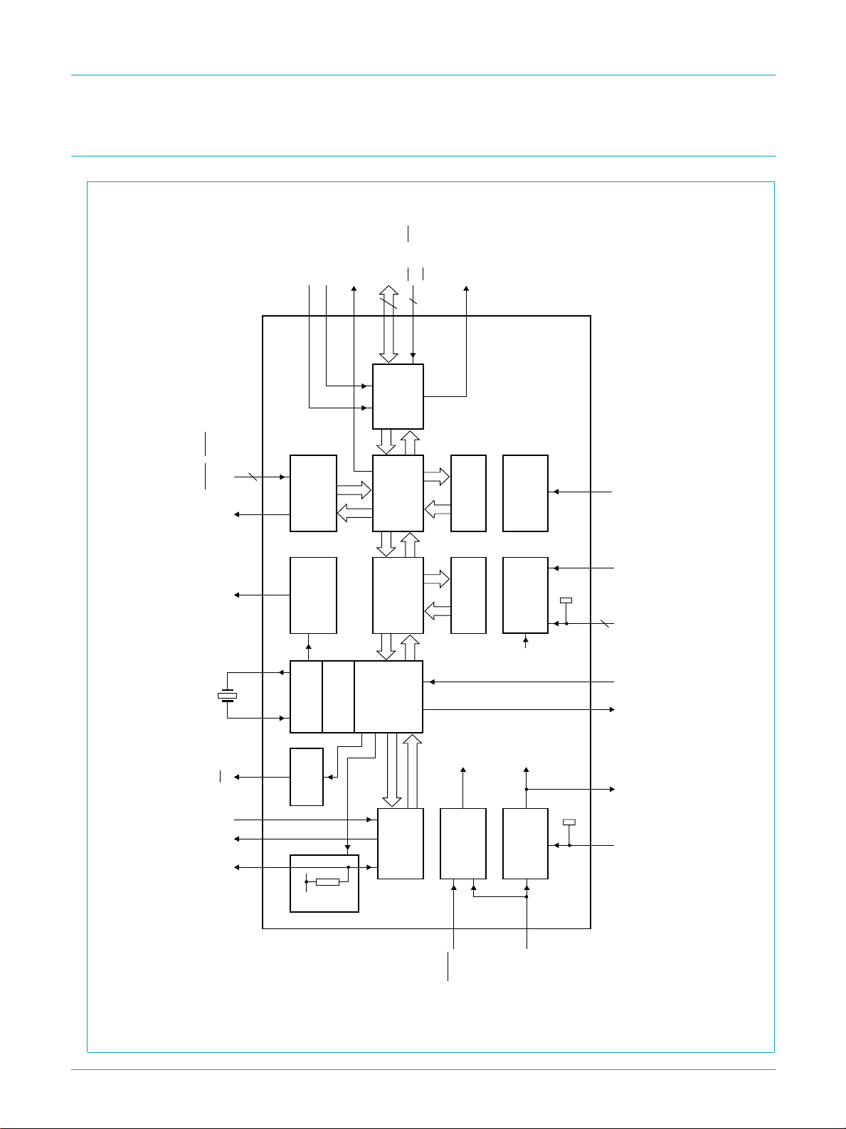
5. Block diagram
ISP1181
Full-speed USB interface
4
SDWR, SDRD,
EOT, DACK
DREQ
XTAL2to LED
6 MHz
GL CLKOUT
sense
input XTAL1
BUS
V
D−
to/from USB
D+
BUS_CONF0
to/from
microcontroller
18
17
13, 14,
10, 12
DMA
11
45
74847
6
4
5
48
PROGR.
MHz
PLL
HUB
HANDLER
DIVIDER
OSCILLATOR
GoodLink
READY
BUS_CONF1
16
38, 35 to 27,
BIT CLOCK
RECOVERY
SoftConnect
CS, ALE, WR,
AD,
DATA1 to DATA9,
16
24 to 19
PHILIPS
RD, A0
DATA10 to DATA15
5
43 to 39
BUS
INTERFACE
MICRO
HANDLER
CONTROLLER
UNIT
MEMORY
MANAGEMENT
SIE
Tx/Rx
ANALOG
INT
15
HANDLER
ENDPOINT
RAM
INTEGRATED
internal
reset
RESET
POWER-ON
ISP1181
I/O PIN
SUPPLY
SUPPLY
INTERNAL
3.3 V
3.3 V
VOLTAGE
REGULATOR
MGS767
26
37
3
25, 36, 46
8
9
3
2
ref(5.0)
V
CC(3.3)
V
GND
WAKEUP
SUSPEND
reg(3.3)
V
REGGND
kΩ
1.5
3.3 V
44
RESET
dbook, full pagewidth
9397 750 06896
1
CC(5.0)
V
© Philips Electronics N.V. 2000. All rights reserved.
Objective specification Rev. 01 — 13 March 2000 3 of 69
Fig 1. Block diagram.

Philips Semiconductors
6. Pinning information
6.1 Pinning
ISP1181
Full-speed USB interface
handbook, halfpage
V
REGGND
V
WAKEUP
SUSPEND
BUS_CONF0
BUS_CONF1
CC(5.0)
reg(3.3)
D−
D+
V
BUS
GL
EOT
DREQ
DACK
SDWR
SDRD
INT
READY
DATA15
DATA14
DATA13
DATA12
DATA11
DATA10
1
2
3
4
5
6
7
8
9
10
11
12
ISP1181DGG
13
14
15
16
17
18
19
20
21
22
23
24
MGL892
48
47
46
45
44
43
42
41
40
39
38
37
36
35
34
33
32
31
30
29
28
27
26
25
XTAL1
XTAL2
GND
CLKOUT
RESET
CS
ALE
WR
RD
A0
AD
V
CC(3.3)
GND
DATA1
DATA2
DATA3
DATA4
DATA5
DATA6
DATA7
DATA8
DATA9
V
ref(5.0)
GND
Fig 2. Pin configuration TSSOP48.
9397 750 06896
Objective specification Rev. 01 — 13 March 2000 4 of 69
© Philips Electronics N.V. 2000. All rights reserved.

Philips Semiconductors
6.2 Pin description
Table 2: Pin description for TSSOP48
Symbol
V
CC(5.0)
REGGND 2 - voltage regulator ground supply
V
reg(3.3)
D− 4 AI/O USB D− connection (analog)
D+ 5 AI/O USB D+ connection (analog)
V
BUS
GL 7 O GoodLink LED indicator output (open-drain, 8 mA); the LED
WAKEUP 8 I wake-up input (edge triggered, LOW to HIGH); generates a
SUSPEND 9 O ‘suspend’ state indicator output (4 mA); used as power switch
EOT 10 I End-Of-Transfer input (programmable polarity, see Table 23);
DREQ 11 O DMA request output (4 mA; programmable polarity, see
DACK 12 I DMA acknowledge input (programmable polarity, see
SDWR 13 I DMA write strobe input; used only in bus configuration
SDRD 14 I DMA read strobe input; used only in bus configuration
INT 15 O interrupt output; programmable polarity (active HIGH or LOW)
READY 16 O I/O ready output; a LOW level indicates that ISP1181 is
BUS_CONF1 17 I bus configuration selector; see Table 3
BUS_CONF0 18 I bus configuration selector; see Table 3
DATA15 19 I/O bit 15 of D[15:0]; bi-directional data line (slew-rate controlled
DATA14 20 I/O bit 14 of D[15:0]; bi-directional data line (slew-rate controlled
[1]
ISP1181
Full-speed USB interface
Pin Type Description
1 - supply voltage (3.0 to 5.5 V)
3 - regulated supply voltage (3.3 V ± 10%) from internal
regulator; used to connect decoupling capacitor and pull-up
resistor on D+ line;
Remark: Cannot be used to supply external devices.
6I V
sensing input
BUS
is default ON, blinks OFF upon USB traffic; to connect an
LED use a 330 Ω series resistor;
remote wake-up from ‘suspend’ state
control output (active LOW) for powered-off application or as
resume signal to the CPU (active HIGH) for powered-on
application
used by the DMA controller to force the end of a DMA transfer
by the ISP1181
Table 23); signals to the DMA controller that the ISP1181
wants to start a DMA transfer
Table 23); used by the DMA controller to signal the start of a
DMA transfer requested by the ISP1181
mode 1 (separate PIO and DMA ports)
mode 1 (separate PIO and DMA ports)
and signalling (level or pulse); see Table 23
processing a previous command or data and is not ready for
the next PIO command or data transfer; a HIGH level signals
that ISP1181 will complete a PIO data transfer; applies only
to a PIO port or a PIO port shared with a DMA port
output, 4 mA)
output, 4 mA)
9397 750 06896
Objective specification Rev. 01 — 13 March 2000 5 of 69
© Philips Electronics N.V. 2000. All rights reserved.

Philips Semiconductors
Table 2: Pin description for TSSOP48
Symbol
DATA13 21 I/O bit 13 of D[15:0]; bi-directional data line (slew-rate controlled
DATA12 22 I/O bit 12 of D[15:0]; bi-directional data line (slew-rate controlled
DATA11 23 I/O bit 11 of D[15:0]; bi-directional data line (slew-rate controlled
DATA10 24 I/O bit 10 of D[15:0]; bi-directional data line (slew-rate controlled
GND 25 - ground supply
V
ref(5.0)
DATA9 27 I/O bit 9 of D[15:0]; bi-directional data line (slew-rate controlled
DATA8 28 I/O bit 8 of D[15:0]; bi-directional data line (slew-rate controlled
DATA7 29 I/O bit 7 of D[15:0]; bi-directional data line (slew-rate controlled
DATA6 30 I/O bit 6 of D[15:0]; bi-directional data line (slew-rate controlled
DATA5 31 I/O bit 5 of D[15:0]; bi-directional data line (slew-rate controlled
DATA4 32 I/O bit 4 of D[15:0]; bi-directional data line (slew-rate controlled
DATA3 33 I/O bit 3 of D[15:0]; bi-directional data line (slew-rate controlled
DATA2 34 I/O bit 2 of D[15:0]; bi-directional data line (slew-rate controlled
DATA1 35 I/O bit 1 of D[15:0]; bi-directional data line (slew-rate controlled
GND 36 - ground supply
V
CC(3.3)
AD 38 I/O multiplexed bi-directional address and data line; represents
A0 39 I address input; selects command (A0 = 1) or data (A0 = 0); in
RD 40 I read strobe input
WR 41 I write strobe input
[1]
ISP1181
Full-speed USB interface
Pin Type Description
output, 4 mA)
output, 4 mA)
output, 4 mA)
output, 4 mA)
26 - I/O pin reference voltage (3.0 to 5.5 V)
output, 4 mA)
output, 4 mA)
output, 4 mA)
output, 4 mA)
output, 4 mA)
output, 4 mA)
output, 4 mA)
output, 4 mA)
output, 4 mA)
37 - supply voltage (3.0 to 3.6 V); leave this pin unconnected
when using the internal regulator
address A0 or bit 0 of D[15:0] in conjunction with input ALE;
level-sensitive input or slew-rate controlled output (4 mA)
Address phase: a HIGH-to-LOW transition on input ALE
latches the level on this pin as address A0 (1 = command,
0 = data)
Data phase: during reading this pin outputs bit D[0]; during
writing the level on this pin is latched as bit D[0]
a multiplexed address/data bus configuration this pin is not
used and must be tied HIGH (connect to V
CC
or V
reg(3.3)
)
9397 750 06896
Objective specification Rev. 01 — 13 March 2000 6 of 69
© Philips Electronics N.V. 2000. All rights reserved.

Philips Semiconductors
Table 2: Pin description for TSSOP48
Symbol
ALE 42 I address latch enable input; a HIGH-to-LOW transition latches
CS 43 I chip select input
RESET 44 I reset input (Schmitt trigger); a LOW level produces an
CLKOUT 45 O programmable clock output (2 mA)
GND 46 - ground supply
XTAL2 47 O crystal oscillator output (6 MHz); connect a fundamental
XTAL1 48 I crystal oscillator input (6 MHz); connect a fundamental
[1]
Pin Type Description
the level on pin AD0 as address information in a multiplexed
address/data bus configuration; must be tied LOW (connect
to DGND) for a separate address/data bus configuration
asynchronous reset; connect to V
(internal POR circuit)
parallel-resonant crystal; leave this pin open when using an
external clock source on pin XTAL1
parallel-resonant crystal or an external clock source (leaving
pin XTAL2 is unconnected)
ISP1181
Full-speed USB interface
for power-on reset
CC
[1] Symbol names with an overscore (e.g. NAME) represent active LOW signals.
7. Functional description
The ISP1181 is a full-speed USB interface device with up to 14 configurable
endpoints. It has a fast general-purpose parallel interface for communication with
many types of microcontrollers or microprocessors. It supports different bus
configurations (see Table 3) and local DMA transfers of up to 16 bytes per cycle. The
block diagram is given in Figure 1.
The ISP1181 has 2462 bytes of internal FIFO memory, which is shared among the
enabled USB endpoints. The type and FIFO size of each endpoint can be individually
configured, depending on the required packet size. Isochronous and bulk endpoints
are double-buffered for increased data throughput. Interrupt IN endpoints can be
configured in rate-feedback mode.
The ISP1181 requires a single supply voltage of 3.0 to 5.5 V and has an internal
3.3 V voltage regulator for powering the analog USB transceiver. It supports
bus-powered operation.
The ISP1181 operates on a 6 MHz oscillator frequency.A programmable clock output
is available up to 48 MHz. During ‘suspend’ state the 24 kHz LazyClock frequency
can be output.
7.1 Analog transceiver
The transceiver is compliant with
interfaces directly with the USB cable through external termination resistors.
9397 750 06896
Objective specification Rev. 01 — 13 March 2000 7 of 69
Universal Serial Bus Specification Rev. 1.1
© Philips Electronics N.V. 2000. All rights reserved.
. It

Philips Semiconductors
7.2 Philips Serial Interface Engine (SIE)
The Philips SIE implements the full USB protocol layer. It is completely hardwired for
speed and needs no firmware intervention. The functions of this block include:
synchronization pattern recognition, parallel/serial conversion, bit (de-)stuffing, CRC
checking/generation, Packet IDentifier (PID) verification/generation, address
recognition, handshake evaluation/generation.
7.3 Memory Management Unit (MMU) and integrated RAM
The MMU and the integrated RAM provide the conversion between the USB speed
(12 Mbit/s bursts) and the parallel interface to the microcontroller (max. 12 Mbyte/s).
This allows the microcontroller to read and write USB packets at its own speed.
7.4 SoftConnect
The connection to the USB is accomplished by bringing D+ (for high-speed USB
devices) HIGH through a 1.5 kΩ pull-up resistor. In the ISP1181 the 1.5 kΩ pull-up
resistor is integrated on-chip and is not connected to VCC by default. The connection
is established through a command sent by the external/system microcontroller. This
allows the system microcontroller to complete its initialization sequence before
deciding to establish connection with the USB. Re-initialization of the USB connection
can also be performed without disconnecting the cable.
ISP1181
Full-speed USB interface
The ISP1181 will check for USB V
established. V
Remark: Note that the tolerance of the internal resistors is 25%. This is higher than
the 5% tolerance specified by the USB specification. However,the overall VSEvoltage
specification for the connection can still be met with a good margin. The decision to
make use of this feature lies with the USB equipment designer.
sensing is provided through pin V
BUS
availability before the connection can be
BUS
.
BUS
7.5 GoodLink
Indication of a good USB connection is provided at pin GL through GoodLink
technology. During enumeration the LED indicator will blink on momentarily. When
the ISP1181 has been successfully enumerated (the device address is set), the LED
indicator will remain permanently on. Upon each successful packet transfer (with
ACK) to and from the ISP1181 the LED will blink off for 100 ms. During ‘suspend’
state the LED will remain off.
This feature provides a user-friendly indicator of the status of the USB device, the
connected hub and the USB traffic. It is a useful field diagnostics tool for isolating
faulty equipment. It can therefor help to reduce field support and hotline overhead.
A register bit can be set to stop the GoodLink LED blinking in traffic (see Table 20).
The LED indicator will then be permanently on.
7.6 Bit clock recovery
The bit clock recovery circuit recovers the clock from the incoming USB data stream
using a 4× over-sampling principle. It is able to track jitter and frequency drift as
specified by the
9397 750 06896
Objective specification Rev. 01 — 13 March 2000 8 of 69
USB Specification Rev. 1.1
.
© Philips Electronics N.V. 2000. All rights reserved.

Philips Semiconductors
7.7 Voltage regulator
A 5 V to 3.3 V voltage regulator is integrated on-chip to supply the analog transceiver
and internal logic. This voltage is available at pin V
pull-up resistor on the D+ line. Alternatively, the ISP1181 provides SoftConnect
technology via an integrated 1.5 kΩ pull-up resistor (see Section 7.4).
7.8 PLL clock multiplier
A 6 MHz to 48 MHz clock multiplier Phase-Locked Loop (PLL) is integrated on-chip.
This allows for the use of a low-cost 6 MHz crystal, which also minimizes EMI. No
external components are required for the operation of the PLL.
7.9 Parallel I/O (PIO) and Direct Memory Access (DMA) interface
A generic PIO interface is defined for speed and ease-of-use. It also allows direct
interfacing to most microcontrollers. To a microcontroller, the ISP1181 appears as a
memory device with an 8/16-bit data bus and an 1-bit address bus. The ISP1181
supports both multiplexed and non-multiplexed address and data buses.
The ISP1181 can also be configured as a DMA slave device to allow more efficient
data transfer. One of the 14 endpoint FIFOs may directly transfer data to/from the
local shared memory. The DMA interface can be configured independently from the
PIO interface.
ISP1181
Full-speed USB interface
to supply an external 1.5 kΩ
reg(3.3)
8. Modes of operation
The ISP1181 has four bus configuration modes, selected via pins BUS_CONF1 and
BUSCONF0:
Mode 0 16-bit I/O port shared with 8-bit or 16-bit DMA port
Mode 1 separate 8-bit I/O port and 8-bit DMA port
Mode 2 8-bit I/O port shared with 8-bit or 16-bit DMA port
Mode 3 reserved.
The bus configurations for each of these modes are given in Table 3. Typical interface
circuits for each mode are given in Section 20.1.
Table 3: Bus configuration modes
Mode BUS_CONF[1:0] PIO width DMA width Description
DMAWD = 0 DMAWD = 1
0 0 0 D[15:0] D[7:0]; D[15:0] multiplexed address/data on pin AD0;
busis shared by 16-bit I/O port and 8-bit
or 16-bit DMA port
1 0 1 D[7:0] D[15:8] illegal multiplexed address/data on pin AD0;
bus has separate I/O port (8-bit) and
DMA port (8-bit)
2 1 0 D[7:0] D[7:0] D[15:0] multiplexed address/data on pin AD0;
bus is shared by 8-bit I/O port and 8-bit
or 16-bit DMA port
3 1 1 reserved reserved reserved reserved
9397 750 06896
Objective specification Rev. 01 — 13 March 2000 9 of 69
© Philips Electronics N.V. 2000. All rights reserved.

Philips Semiconductors
9. Endpoint descriptions
Each USB device is logically composed of several independent endpoints. An
endpoint acts as a terminus of a communication flow between the host and the
device. At design time each endpoint is assigned a unique number (endpoint
identifier, see Table 4). The combination of the device address (given by the host
during enumeration), the endpoint number and the transfer direction allows each
endpoint to be uniquely referenced.
The ISP1181 has 16 endpoints: endpoint 0 (control IN and OUT) plus 14 configurable
endpoints, which can be individually defined as interrupt/bulk/isochronous,IN or OUT.
Each enabled endpoint has an associated FIFO, which can be accessed either via
the parallel I/O interface or via DMA.
9.1 Endpoint access
Table 4 lists the endpoint access modes and programmability. All endpoints support
I/O mode access. Endpoints 1 to 14 also support DMA access. FIFO DMA access is
selected and enabled via bits EPIDX[3:0] and DMAEN of the DMA Configuration
Register. A detailed description of the DMA operation is given in Section 10.
ISP1181
Full-speed USB interface
Table 4: Endpoint access and programmability
Endpoint
identifier
0 64 (fixed) no yes no control OUT
0 64 (fixed) no yes no control IN
1 programmable supported supported supported programmable
2 programmable supported supported supported programmable
3 programmable supported supported supported programmable
4 programmable supported supported supported programmable
5 programmable supported supported supported programmable
6 programmable supported supported supported programmable
7 programmable supported supported supported programmable
8 programmable supported supported supported programmable
9 programmable supported supported supported programmable
10 programmable supported supported supported programmable
11 programmable supported supported supported programmable
12 programmable supported supported supported programmable
13 programmable supported supported supported programmable
14 programmable supported supported supported programmable
[1] IN: input for the USB host (ISP1181 transmits); OUT: output from the USB host (ISP1181 receives).
[2] The data flow direction is determined by bit EPDIR in the Endpoint Configuration Register.
[3] The total amount of FIFO storage allocated to enabled endpoints must not exceed 2462 bytes.
FIFO size (bytes) Double
buffering
I/O mode
access
DMA mode
access
Endpoint type
[1]
[1]
9397 750 06896
Objective specification Rev. 01 — 13 March 2000 10 of 69
© Philips Electronics N.V. 2000. All rights reserved.

Philips Semiconductors
9.2 Endpoint FIFO size
The size of the FIFO determines the maximum packet size that the hardware can
support for a given endpoint. Only enabled endpoints are allocated space in the
shared FIFO storage, disabled endpoints have zero bytes. Table 5 lists the
programmable FIFO sizes.
The following bits in the Endpoint Configuration Register (ECR) affect FIFO
allocation:
•
•
•
Remark: Register changes that affect the allocation of the shared FIFO storage
among endpoints must not be made while valid data is present in any FIFO of the
enabled endpoints. Such changes will render all FIFO contents undefined.
Table 5: Programmable FIFO size
FFOSZ[3:0] Non-isochronous Isochronous
0000 8 bytes 16 bytes
0001 16 bytes 32 bytes
0010 32 bytes 48 bytes
0011 64 bytes 64 bytes
0100 reserved 96 bytes
0101 reserved 128 bytes
0110 reserved 160 bytes
0111 reserved 192 bytes
1000 interrupt IN 8 bytes,
1001 interrupt IN 16 bytes,
1010 interrupt IN 32 bytes,
1011 interrupt IN 64 bytes,
1100 reserved 640 bytes
1101 reserved 768 bytes
1110 reserved 896 bytes
1111 reserved 1023 bytes
ISP1181
Full-speed USB interface
endpoint enable bit (FIFOEN)
size bits of an enabled endpoint (FFOSZ[3:0])
isochronous bit of an enabled endpoint (FFOISO).
256 bytes
rate feedback mode
320 bytes
rate feedback mode
384 bytes
rate feedback mode
512 bytes
rate feedback mode
Each programmable FIFO can be configured independently via its ECR, but the total
physical size of all enabled endpoints (IN plus OUT) must not exceed 2462 bytes
(512 bytes for non-isochronous FIFOs).
Table 6 shows an example of a configuration fitting in the maximum available space of
2462 bytes. The total number of logical bytes in the example is 1311. The physical
storage capacity used for double buffering is managed by the device hardware and is
transparent to the user.
9397 750 06896
Objective specification Rev. 01 — 13 March 2000 11 of 69
© Philips Electronics N.V. 2000. All rights reserved.

Philips Semiconductors
Table 6: Memory configuration example
Physical size
(bytes)
64 64 control IN (64 byte fixed)
64 64 control OUT (64 byte fixed)
2046 1023 double-buffered 1023-byte isochronous endpoint
16 16 16-byte interrupt OUT
16 16 16-byte interrupt IN
128 64 double-buffered 64-byte bulk OUT
128 64 double-buffered 64-byte bulk IN
9.3 Endpoint initialization
In response to the standard USB request Set Interface,the firmware must program all
16 ECRs of the ISP1181 in sequence (see Table 4), whether the endpoints are
enabled or not. The hardware will then automatically allocate FIFO storage space.
If all endpoints havebeen configured successfully,the firmware must return an empty
packet to the control IN endpoint to acknowledge success to the host. If there are
errors in the endpoint configuration, the firmware must stall the control IN endpoint.
Logical size
(bytes)
ISP1181
Full-speed USB interface
Endpoint description
When reset by hardware or via the USB bus, the ISP1181 disables all endpoints and
clears all ECRs, except for the control endpoint which is fixed and always enabled.
Endpoint initialization can be done at any time; however, it is valid only after
enumeration.
9.4 Endpoint I/O mode access
When an endpoint event occurs (a packet is transmitted or received), the associated
endpoint interrupt bits (EPn) of the Interrupt Register (IR) will be set by the SIE. The
firmware then responds to the interrupt and selects the endpoint for processing.
The endpoint interrupt bit will be cleared by reading the Endpoint Status Register
(ESR). The ESR also contains information on the status of the endpoint buffer.
For an OUT (= receive) endpoint, the packetlength and packet data can be read from
ISP1181 using the Read Buffer command. When the whole packet has been read,
the firmware sends a Clear Buffer command to enable the reception of new packets.
For an IN (= transmit) endpoint, the packet length and data to be sent can be written
to ISP1181 using the Write Buffer command. When the whole packet has been
written to the buffer, the firmware sends a Validate Buffer command to enable data
transmission to the host.
9.5 Special actions on control endpoints
Control endpoints require special firmware actions. The arrival of a SETUP packet
flushes the IN buffer and disables the Validate Buffer and Clear Buffer commands for
the control IN and OUT endpoints. The microcontroller needs to re-enable these
commands by sending an Acknowledge Setup command to both control endpoints.
9397 750 06896
Objective specification Rev. 01 — 13 March 2000 12 of 69
© Philips Electronics N.V. 2000. All rights reserved.

Philips Semiconductors
This ensures that the last SETUP packet stays in the buffer and that no packets can
be sent back to the host until the microcontroller has explicitly acknowledged that it
has seen the SETUP packet.
10. DMA transfer
Direct Memory Access (DMA) is a method to transfer data from one location to
another in a computer system, without intervention of the central processor (CPU).
Many different implementations of DMA exist. The ISP1181 supports two methods:
•
•
The ISP1181 supports DMA transfer for all 14 configurable endpoints (see Table 4).
Only one endpoint at a time can be selected for DMA transfer. The DMA operation of
the ISP1181 can be interleaved with normal I/O mode access to other endpoints.
ISP1181
Full-speed USB interface
8237 compatible mode: based on the DMA subsystem of the IBM personal
computers (PC, AT and all its successors and clones); this architecture uses the
Intel 8237 DMA controller and has separate address spaces for memory and I/O
DACK-only mode: based on the DMA implementation in some embedded RISC
processors, which has a single address space for both memory and I/O.
The following features are supported:
Single-cycle or burst transfers (up tot 16 bytes per cycle)
•
Programmable transfer direction (read or write)
•
Multiple End-Of-Transfer (EOT) sources: external pin, internal conditions,
•
short/empty packet
Programmable signal levels on pins DREQ, DACK and EOT
•
Automatic DMA counter reload and transfer restart following EOT.
•
10.1 Selecting an endpoint for DMA transfer
The target endpoint for DMA access is selected via bits EPDIX[3:0] in the DMA
Configuration Register, as shown in Table 7. The transfer direction (read or write) is
automatically set by bit EPDIR in the associated ECR, to match the selected endpoint
type (OUT endpoint: read; IN endpoint: write).
Asserting input DACK automatically selects the endpoint specified in the DMA
Configuration Register, regardless of the current endpoint used for I/O mode access.
Table 7: Endpoint selection for DMA transfer
Endpoint
identifier
1 0010 OUT: read IN: write
2 0011 OUT: read IN: write
3 0100 OUT: read IN: write
4 0101 OUT: read IN: write
5 0110 OUT: read IN: write
6 0111 OUT: read IN: write
7 1000 OUT: read IN: write
EPIDX[3:0] Transfer direction
EPDIR = 0 EPDIR = 1
9397 750 06896
Objective specification Rev. 01 — 13 March 2000 13 of 69
© Philips Electronics N.V. 2000. All rights reserved.

Philips Semiconductors
Table 7: Endpoint selection for DMA transfer
10.2 8237 compatible mode
The 8237 compatible DMA mode is selected by clearing bit DAKOLY in the Hardware
Configuration Register (see Table 22). The pin functions for this mode are shown in
Table 8.
Table 8: 8237 compatible mode: pin functions
Symbol Description I/O Function
DREQ DMA request O ISP1181 requests a DMA transfer
DACK DMA acknowledge I DMA controller confirms the transfer
EOT end of transfer I DMA controller terminates the transfer
RD read strobe I instructs ISP1181 to put data on the bus
WR write strobe I instructs ISP1181 to get data from the bus
Full-speed USB interface
Endpoint
identifier
8 1001 OUT: read IN: write
9 1010 OUT: read IN: write
10 1011 OUT: read IN: write
11 1100 OUT: read IN: write
12 1101 OUT: read IN: write
13 1110 OUT: read IN: write
14 1111 OUT: read IN: write
EPIDX[3:0] Transfer direction
EPDIR = 0 EPDIR = 1
ISP1181
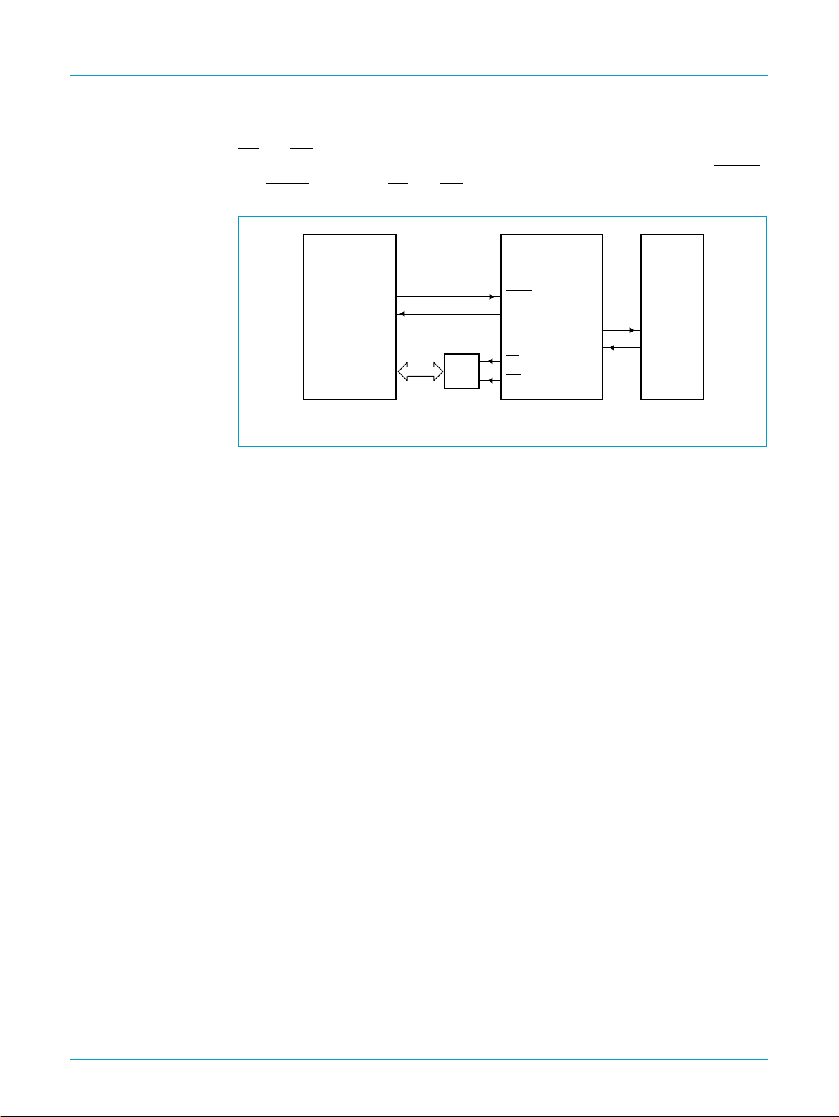
The DMA subsystem of an IBM compatible PC is based on the Intel 8237 DMA
controller. It operates as a ‘fly-by’ DMA controller: the data is not stored in the DMA
controller, but it is transferred between an I/O port and a memory address. A typical
example of ISP1181 in 8237 compatible DMA mode is given in Figure 3.
The 8237 has two control signals for each DMA channel: DRQ (DMA Request) and
DACK (DMA Acknowledge). General control signals are HRQ (Hold Request), HLDA
(Hold Acknowledge) and EOP (End-Of-Process). The bus operation is controlled via
MEMR (Memory Read), MEMW (Memory Write), IOR (I/O read) and IOW (I/O write).
dth
DATA1 to DATA15
AD,
ISP1181
DREQ
DACK
RD
WR
RAM
Fig 3. ISP1181 in 8237 compatible DMA mode.
MEMR
MEMW
DMA
CONTROLLER
8237
DREQ HRQ
DACK
IOR
IOW
HLDA
CPU
HRQ
HLDA
MGS778
9397 750 06896
Objective specification Rev. 01 — 13 March 2000 14 of 69
© Philips Electronics N.V. 2000. All rights reserved.

Philips Semiconductors
The following example shows the steps which occur in a typical DMA transfer:
1. ISP1181 receives a data packet in one of its endpoint FIFOs; the packet must be
2. ISP1181 asserts the DREQ signal requesting the 8237 for a DMA transfer.
3. The 8237 asks the CPU to release the bus by asserting the HRQ signal.
4. After completing the current instruction cycle, the CPU places the bus control
5. The 8237 now sets its address lines to 1234H and activates the MEMW and IOR
6. The 8237 asserts DACK to inform the ISP1181 that it will start a DMA transfer.
7. TheISP1181 now places the byte or word to be transferredon the data bus lines,
8. The8237 waits one DMA clock period and then de-asserts MEMW and IOR. This
9. The ISP1181 de-asserts the DREQ signal to indicate to the 8237 that DMA is no
10. The 8237 de-asserts the DACK output indicating that the ISP1181 must stop
11. The 8237 places the bus control signals (MEMR, MEMW, IOR and IOW) and the
12. The CPU acknowledges control of the bus by de-asserting HLDA. After activating
ISP1181
Full-speed USB interface
transferred to memory address 1234H.
signals (MEMR, MEMW, IOR and IOW) and the address lines in three-state and
asserts HLDA to inform the 8237 that it has control of the bus.
control signals.
because its RD signal was asserted by the 8237.
latches and stores the byte or word at the desired memory location. It also
informs the ISP1181 that the data on the bus lines has been transferred.
longer needed. In Single cycle mode this is done after each byte or word, in
Burst mode following the last transferred byte or word of the DMA cycle.
placing data on the bus.
address lines in three-state and de-asserts the HRQ signal, informing the CPU
that it has released the bus.
the bus control lines (MEMR, MEMW, IOR and IOW) and the address lines, the
CPU resumes the execution of instructions.
Fora typical bulk transfer the aboveprocess is repeated 64 times, once for each byte.
After each byte the address register in the DMA controller is incremented and the
byte counter is decremented. When using 16-bit DMA the number of transfers is 32
and address incrementing and byte counter decrementing is done by 2 for each word.
10.3 DACK-only mode
The DACK-only DMA mode is selected by setting bit DAKOLY in the Hardware
Configuration Register (see Table 22). The pin functions for this mode are shown in
Table 9. A typical example of ISP1181 in DACK-only DMA mode is given in Figure 4.
Table 9: DACK-only mode: pin functions
Symbol Description I/O Function
DREQ DMA request O ISP1181 requests a DMA transfer
DACK DMA acknowledge I DMA controller confirms the transfer;
also functions as data strobe
EOT End-Of-Transfer I DMA controller terminates the transfer
RD read strobe I not used
WR write strobe I not used
9397 750 06896
Objective specification Rev. 01 — 13 March 2000 15 of 69
© Philips Electronics N.V. 2000. All rights reserved.
Philips Semiconductors
In DACK-only mode the ISP1181 uses the DACK signal as data strobe. Input signals
RD and WR are ignored. This mode is used in CPU systems that have a single
address space for memory and I/O access. Such systems have no separate MEMW
and MEMR signals: the RD and WR signals are also used as memory data strobes.
ISP1181
Full-speed USB interface
dth
Fig 4. ISP1181 in DACK-only DMA mode.
ISP1181 DMA
DREQ
DACK
AD,
DATA1 to DATA15
10.4 End-Of-Transfer conditions
10.4.1 Bulk endpoints
A DMA transfer to/from a bulk endpoint can be terminated by any of the following
conditions (bit names refer to the DMA Configuration Register, see Table 26):
An external End-Of-Transfer signal occurs on input EOT
•
The internal DMA Counter Register reaches zero (CNTREN = 1)
•
A short/empty packet is received on an enabled OUT endpoint (SHORTP = 1)
•
DMA operation is disabled by clearing bit DMAEN.
•
RAM
CONTROLLER
DREQ
DACK
RD
WR
HRQ
HLDA
CPU
HRQ
HLDA
MGS779
External EOT: When reading from an OUT endpoint, an external EOT will stop the
DMA operation and clear any remaining data in the current FIFO. For a doublebuffered endpoint the other (inactive) buffer is not affected.
When writing to an IN endpoint, an EOT will stop the DMA operation and the data
packet in the FIFO (even if it is smaller than the maximum packet size) will be sent to
the USB host at the next IN token.
DMA Counter Register zero: An EOT from the DMA Counter Register is enabled by
setting bit CNTREN in the DMA Configuration Register. The ISP1181 has a 16-bit
DMA Counter Register, which specifies the number of bytes to be transferred. When
DMA is enabled (DMAEN = 1), the internal DMA counter is loaded with the value from
the DMA Counter Register.When the internal counter reaches zero an EOTcondition
is generated and the DMA operation stops.
Short/empty packet: Normally, the transfer byte count must be set via a control
endpoint before any DMA transfer takes place. When a short/empty packet has been
enabled as EOT indicator (SHORTP = 1), the transfer size is determined by the
presence of a short/empty packet in the data. This mechanism permits the use of a
fully autonomous data transfer protocol.
9397 750 06896
Objective specification Rev. 01 — 13 March 2000 16 of 69
© Philips Electronics N.V. 2000. All rights reserved.

Philips Semiconductors
When reading from an OUT endpoint, reception of a short/empty packet at an OUT
token will stop the DMA operation after transferring the data bytes of this packet.
When writing to an IN endpoint, a short packet transferred at an IN token will stop the
DMA operation after all bytes have been transferred. If the number of bytes in the
buffer is zero, ISP1181 will automatically send an empty packet.
Table 10: Summary of EOT conditions for a bulk endpoint
EOT condition OUT endpoint IN endpoint
EOT input EOT is active EOT is active
DMA Counter Register counter reaches zero counter reaches zero
Short packet short packet is received and
Empty packet empty packet is received and
DMAEN bit in DMA
Configuration Register
[1] If short/empty packet EOT is enabled (SHORTP = 1 in DMA Configuration Register) and DMA
Counter Register is zero.
Full-speed USB interface
counter reaches zero in the
transferred
transferred
DMAEN = 0 DMAEN = 0
middle of the buffer
empty packet is automatically
appended when needed
ISP1181
[1]
10.4.2 Isochronous endpoints
A DMA transfer to/from an isochronous endpoint can be terminated by any of the
following conditions (bit names refer to the DMA Configuration Register, see
Table 26):
An external End-Of-Transfer signal occurs on input EOT
•
The internal DMA Counter Register reaches zero (CNTREN = 1)
•
An End-Of-Packet (EOP) signal is detected
•
DMA operation is disabled by clearing bit DMAEN.
•
Table 11: Recommended EOT usage for isochronous endpoints
EOT condition OUT endpoint IN endpoint
EOT input active do not use preferred
DMA Counter Register zero do not use preferred
End-Of-Packet preferred do not use
10.4.3 DMA auto-restart
If the AUTOLD bit in the DMA Configuration Register is set, the DMA operation will
automatically restart when the last transfer has been completed. First the internal
DMA counter is reloaded from of the DMA Counter Register. Output DREQ is then
asserted to request a new DMA transfer for an IN endpoint, or when the buffer of an
OUT endpoint buffer has been filled.
9397 750 06896
Objective specification Rev. 01 — 13 March 2000 17 of 69
© Philips Electronics N.V. 2000. All rights reserved.

Philips Semiconductors
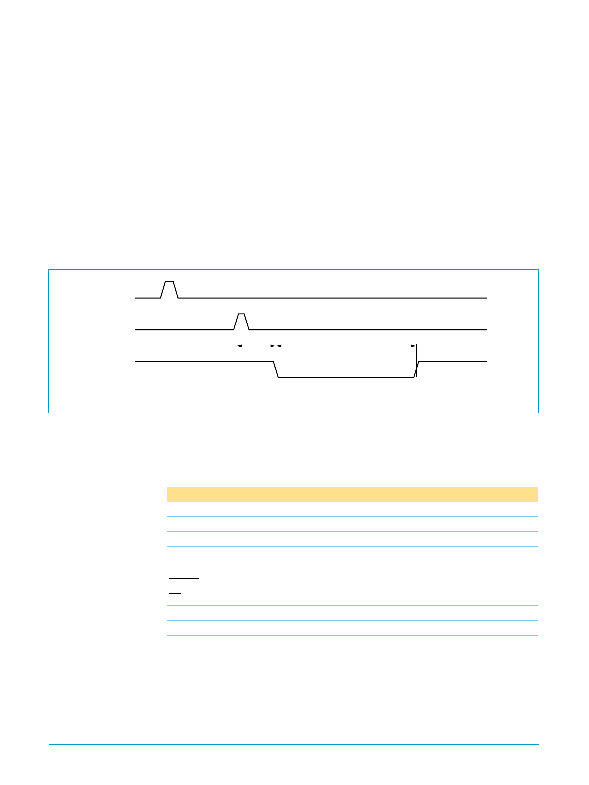
11. Suspend and resume
11.1 Suspend conditions
The ISP1181 detects a USB ‘suspend’ status in the following cases:
A J-state is present on the USB bus for 3 ms
•
V
•
•
ISP1181 will remain in ‘suspend’ state for at least 5 ms, before responding to external
wake-up events such as global resume, bus traffic, wake-up on CS or WAKEUP. The
typical timing is shown in Figure 5.
is lost (weak pull-up/down on D+ and D−)
BUS
SoftConnect is disabled by clearing bit SOFTCT in the Mode Register, with
external pull-ups disabled by EXTPUL = 0 in the Hardware Configuration Register.
In this situation ISP1181 is effectively disconnected from the USB bus.
ISP1181
Full-speed USB interface
handbook, full pagewidth
Fig 5. Typical suspend timing.
GOSUSP
WAKEUP
Bus-powered devices that are suspended must not consume more than 500 µA of
current. This is achieved by shutting down the power to system components or
supplying them with a reduced voltage.
ISP1181 can either be in powered-on or powered-off mode during ‘suspend’ state.
This is controlled by bit PWROFF in the Hardware Configuration Register. A full
explanation of these modes is given in Section 11.1.1 and Section 11.1.2.
The steps leading up to ‘suspend’ status are as follows:
1. Upon detection of a ‘wake-up’ to ‘suspend’ transition ISP1181 sets bit SUSPND
2. When the firmware detects a ‘suspend’ condition it must prepare all system
3. In the interrupt service routine the firmware must check the current status of the
suspend
>5 ms
start detection of
wake-up conditions
MGS949
in the Interrupt Register. This will generate an interrupt if bit IESUSP in the
Interrupt Enable Register is set.
components for ‘suspend’ state:
a. All signals connected to ISP1181 must enter appropriate states to meet the
power consumption requirements of ‘suspend’ state.
b. All input pins of ISP1181 must have a CMOS logic 0 or logic 1 level. Pin
settings differ for powered-on and powered-off application.
USB bus. When bit BUSTATUS in the Interrupt Register is logic 0, the USB bus
has left ‘suspend’ mode and the process must be aborted. Otherwise, the next
step can be executed.
9397 750 06896
Objective specification Rev. 01 — 13 March 2000 18 of 69
© Philips Electronics N.V. 2000. All rights reserved.
Philips Semiconductors
4. To meet the ‘suspend’ current requirements for a bus-powered device, the
5. When the firmware has set and cleared the GOSUSP bit in the Mode Register,
11.1.1 Powered-on application
In powered-on application (PWROFF = 0 in the Hardware Configuration Register) the
power supply of the CPU and other parts of the circuit is not switched off. The CPU is
normally placed in low-power mode. The SUSPEND output of ISP1181 is normally
HIGH and pulses LOW for 10 ms upon a ‘resume’ condition. This signal can be used
to wake up the CPU. The signal timing is shown in Figure 6.
ISP1181
Full-speed USB interface
internal clocks must be switched off by clearing bit CLKRUN in the Hardware
Configuration Register.
the ISP1181 enters ‘suspend’ state. In powered-off application, the ISP1181
asserts output SUSPEND and switches off the internal clocks after 2 ms.
handbook, full pagewidth
Fig 6. Suspend and resume timing for powered-on application.
GOSUSP
WAKEUP
0.5 ms 10 ms
SUSPEND
In powered-on application ISP1181 drives its output pins, while the inputs are driven
by the application. Bi-directional pins are placed in three-state and driven HIGH or
LOW by the application. A summary of appropriate pin states is given in Table 12.
Table 12: Pin states in powered-on application
Pin Type Appropriate state
A0 I/O (three-state) externally driven
DATA[15:0] I/O (three-state) depends on state of inputs
SUSPEND O ISP1181 drives logic 1
WAKEUP I externally driven to logic 1
INT O (three-state) ISP1181 drives logic 0 or logic 1
RESET I externally driven to logic 1
CS I externally driven to logic 0 or logic 1 (default: logic 1)
RD I externally driven to logic 0 or logic 1 (default: logic 1)
WR I externally driven to logic 1
XTAL1 I externally driven to logic 1, if external oscillator is used
CLKOUT O (three-state) ISP1181 drives logic 0
[1]
to logic 0 or logic 1
RD and CS
MGS780
[1] ‘Externally driven’ refers to logic outside the ISP1181.
9397 750 06896
Objective specification Rev. 01 — 13 March 2000 19 of 69
© Philips Electronics N.V. 2000. All rights reserved.

Philips Semiconductors
The USB connections D+ and D− remain powered and logically connected to the
USB bus. If a crystal oscillator is used, powering down during ‘suspend’ is managed
by the internal logic of ISP1181. When using an external oscillator on pin XTAL1, a
stable logic 1 level must be applied during ‘suspend’ state.
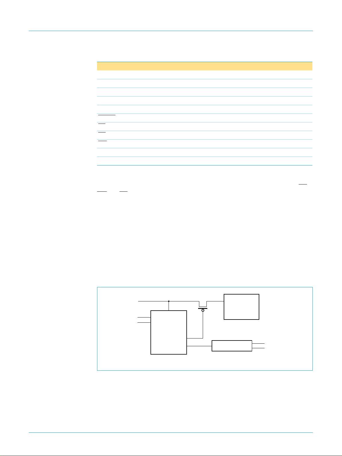
Figure 7 shows a typical bus-powered modem application using ISP1181 in
powered-onmode. The SUSPEND output is connected to the reset input (RST) of the
8031 microcontroller via an external inverter.This allowsa ‘resume’ condition to wake
up the 8031 from power-down mode. The ISP1181 is woken up via the USB bus
(global resume) or by the ring detection circuit on the telephone line.
ISP1181
Full-speed USB interface
dth
USB
V
BUS
D+
D−
Fig 7. SUSPEND and WAKEUP signals in a powered-on modem application.
11.1.2 Powered-off application
In powered-off application (PWROFF = 1 in the Hardware Configuration Register) the
supply of the CPU and other parts of the circuit is removed during ‘suspend’ state.
The SUSPEND output is active HIGH during ‘suspend’ state, making it suitable as a
power switch control signal, e.g. for an external oscillator.
Input pins of ISP1181 are pulled to ground via the pin buffers. Outputs are made
three-state to prevent current flowing in the application. Bi-directional pins are made
three-state and must be pulled to ground externally by the application. The power
supply of external pull-ups must also be removed to reduce power consumption.
V
CC(5.0)
ISP1181
SUSPEND
WAKEUP
V
CC
8031
RST
RING DETECTION
LINE
MGS781
handbook, full pagewidth
GOSUSP
WAKEUP
2 ms 0.5 ms
SUSPEND
MGS782
Fig 8. Suspend and resume timing for powered-off application.
9397 750 06896
Objective specification Rev. 01 — 13 March 2000 20 of 69
© Philips Electronics N.V. 2000. All rights reserved.
Philips Semiconductors
Table 13: Pin states in powered-off application
Pin Type Appropriate state
A0 I/O (three-state) powered off; internally connected to ground (logic 0)
DATA[15:0] I/O (three-state) powered off; internally connected to ground (logic 0)
SUSPEND O ISP1181 drives logic 1
WAKEUP I powered off; internally connected to ground (logic 0)
INT O (three-state) powered off; internally connected to ground (logic 0)
RESET I externally driven
CS I powered off; internally connected to ground (logic 0)
RD I powered off; internally connected to ground (logic 0)
WR I powered off; internally connected to ground (logic 0)
XTAL1 I powered off; internally connected to ground (logic 0)
CLKOUT O (three-state) ISP1181 drives logic 0
[1] ‘Externally driven’ refers to logic outside the ISP1181.
When external components are powered-off, it is possible that interface signals RD,
WR and CS have unknown values immediately after leaving ‘suspend’ state. To
prevent corruption of its internal registers, ISP1181 enables a locking mechanism
once suspend is enabled.
[1]
to logic 1
ISP1181
Full-speed USB interface
After wake-up from suspend’ state, all internal registers except the Unlock Register
are write-protected. A special unlock operation is needed to re-enable write access.
This prevents data corruption during power-up of external components.
Figure 9 shows a typical bus-powered modem application using ISP1181 in
powered-off mode. The SUSPEND output is used to switch off power to the
microcontroller and other external circuits during ‘suspend’ state. The ISP1181 is
woken up via the USB bus (global resume) or by the ring detection circuit on the
telephone line.
dth
Fig 9. SUSPEND and WAKEUP signals in a powered-off modem application.
USB
V
BUS
D+
D−
V
CC(5.0)
ISP1181
SUSPEND
WAKEUP
V
power
switch
CC
CONTROLLER
RING DETECTION
MICRO-
LINE
MGS783
9397 750 06896
Objective specification Rev. 01 — 13 March 2000 21 of 69
© Philips Electronics N.V. 2000. All rights reserved.
 Loading...