

Philips ISP1161BM, ISP1161BD Datasheet

ISP1161
Full-speed Universal Serial Bus single-chip host and device
controller
Rev. 01 — 3 July 2001 Product data
1. General description
The ISP1161 is a single-chip Universal Serial Bus (USB) Host Controller (HC) and
Device Controller (DC) which complies with
Rev 1.1
microprocessor bus interface. They have the same data bus, but different I/O
locations. They also have separate interrupt request output pins, separate DMA
channels that include separate DMA request output pins and DMA acknowledge
input pins. This makes it possible for a microprocessor to control both the USB HC
and the USB DC at the same time.
ISP1161 provides two downstream ports for the USB HC and one upstream port for
the USB DC. Each downstream port has its own overcurrent (OC) detection input pin
and power supply switching control output pin. The upstream port has its own V
detection input pin. ISP1161 also provides separate wakeup input pins and
suspended status output pins for the USB HC and the USB DC, respectively. This
makes power management flexible. The downstream ports for the HC can be
connected with any USB compliant USB devices and USB hubs that have USB
upstream ports. The upstream port for the DC can be connected to any USB
compliant USB host and USB hubs that have USB downstream ports.
c
c
The DC is compliant with most device class specifications such as Imaging Class,
Mass Storage Devices, Communication Devices, Printing Devices and Human
Interface Devices.
Universal Serial Bus Specification
. These two USB controllers, the HC and the DC, share the same
BUS
ISP1161 is well suited for embedded systems and portable devices that require a
USB host only, a USB device only, or a combined and configurable USB host and
USB device capabilities. ISP1161 brings high flexibility to the systems that have it
built-in. For example, a system that has ISP1161 built-in allows it not only to be
connected to a PC or USB hub that has a USB downstream port, but also to be
connected to a device that has a USB upstream port such as a USB printer, USB
camera, USB keyboard, USB mouse, among others. ISP1161 enables peer-to-peer
connectivity between embedded systems. An interesting application example is to
connect a ISP1161 HC with a ISP1161 DC.
Let us see an example of ISP1161beingusedinaDigitalStillCamera(DSC)design.
Figure 1 shows ISP1161 being used as a USB DC. Figure 2 shows ISP1161 being
used as a USB HC. Figure 3 shows ISP1161 being used as a USB HC and a USB
DC at the same time.

Philips Semiconductors
ISP1161
Full-speed USB single-chip host and device controller
EMBEDDED SYSTEM
PC
(host)
USB cable
USB I/F
USB I/F
Fig 1. ISP1161 operating as a USB device.
EMBEDDED SYSTEM
ISP1161
HOST/
DEVICE
µP SYSTEM
MEMORY
µP bus I/F
USB host
USB I/F
µP
DSC
µP
USB device
USB cable
µP SYSTEM
MEMORY
µP bus I/F
ISP1161
HOST/
DEVICE
DSC
MGT926
PRINTER
(device)
USB I/F
MGT927
Fig 2. ISP1161 operating as a stand-alone USB host.
9397 750 08313
Product data Rev. 01 — 3 July 2001 2 of 130
© Philips Electronics N.V. 2001. All rights reserved.

Philips Semiconductors
ISP1161
Full-speed USB single-chip host and device controller
EMBEDDED SYSTEM
ISP1161
HOST/
DEVICE
µP SYSTEM
MEMORY
µP bus I/F
USB host
PRINTER
(device)
USB I/FUSB I/F
USB I/F
MGT928
µP
PC
(host)
USB cable USB cable
Fig 3. ISP1161 operating as both USB host and device simultaneously.
DSC
USB I/F
USB device
2. Features
■ Complies with
■ Combines HC and DC in a single chip
■ On-chip DC complies with most Device Class specifications
■ Both HC and DC can be accessed by an external microprocessor via separate I/O
port addresses
■ Selectable one or two downstream ports for HC and one upstream port for DC
■ High speed parallel interface to most of the generic microprocessors and
Reduced Instruction Set Computer (RISC) processors (Hitachi SH-3 and SH-4,
MIPS-based RISC, ARM7/9, StrongARM, etc.). Maximum 15 Mbyte/s data
transfer rate between microprocessor and the HC, 11.1 Mbyte/s data transfer rate
between microprocessor and the DC
■ Supports single-cycle burst mode and multiple-cycle burst mode DMA operations
■ Up to 14 programmable USB endpoints with 2 fixed control IN/OUT endpoints for
the DC
■ Built in separate FIFO buffer RAM for HC (4 kbytes) and DC (2462 bytes)
■ Endpoints with double buffering to increase throughput and ease real-time data
transfer for both DC transfers and HC isochronous (ISO) transactions
■ 6 MHz crystal oscillator with integrated PLL for low EMI
■ Controllable LazyClock (24 kHz) output during ‘suspend’
■ Clock output with programmable frequency (3 to 48 MHz)
■ Software controlled connection to the USB bus (SoftConnect) on upstream port
for the DC
■ Good USB connection indicator that blinks with traffic (GoodLink) for the DC
■ Built-in software selectable internal 15 kΩ pull-down resistors for HC downstream
ports
■ Dedicated pins for suspend sensing output and wakeup control input for flexible
applications
■ Global hardware reset input pin and separate internal software reset circuits for
HC and DC
9397 750 08313
Product data Rev. 01 — 3 July 2001 3 of 130
Universal Serial Bus Specification Rev 1.1
© Philips Electronics N.V. 2001. All rights reserved.

Philips Semiconductors
■ Operation at either +5 V or +3.3 V power supply input
■ 8 kV in-circuit ESD protection
■ Operating temperature range −40 to +85 °C
■ Available in two LQFP64 packages (SOT314-2 and SOT414-1).
3. Applications
■ Personal Digital Assistant (PDA)
■ Digital camera
■ Third-generation (3-G) phone
■ Set-top box (STB)
■ Information Appliance (IA)
■ Photo printer
■ MP3 jukebox
■ Game console.
4. Ordering information
ISP1161
Full-speed USB single-chip host and device controller
Table 1: Ordering information
Type number Package
Name Description Version
ISP1161BD LQFP64 Plastic low profile quad flat package; 64 leads; body 10 x 10 x 1.4 mm SOT314-2
ISP1161BM LQFP64 Plastic low profile quad flat package; 64 leads; body 7 x 7 x 1.4 mm SOT414-1
9397 750 08313
Product data Rev. 01 — 3 July 2001 4 of 130
© Philips Electronics N.V. 2001. All rights reserved.

9397 750 08313
Product data Rev. 01 — 3 July 2001 5 of 130
6 MHz
5. Block diagram
Philips Semiconductors
to/from
microprocessor
H_WAKEUP
H_SUSPEND
NDP_SEL
D0 to D15
RD
CS
WR
A1
A0
DACK2
DACK1
EOT
DREQ2
DREQ1
INT2
INT1
D_WAKEUP
D_SUSPEND
RESET
V
CC
© Philips Electronics N.V. 2001. All rights reserved.
Fig 4. Block diagram.
XTAL1XTAL2
DIVIDER
413819
CLKOUT
43
OVERCURRENT
TRANSCEIVER
TRANSCEIVER
TRANSCEIVER
SoftConnect
POWER
SWITCHING
DETECTION
USB
USB
4×
15 kΩ
USB
n.c.
GND
1.5 kΩ
61, 20
2
3.3 V
46
47
54
55
50
51
52
53
39
48
49
MGT929
H_PSW1
H_PSW2
H_OC1
H_OC2
H_DM1
H_DP1
H_DM2
H_DP2
D_VBUS
D_DM
D_DP
USB bus
downstream
ports
USB bus
upstream
port
Full-speed USB single-chip host and device controller
40
42
33
2 to 7,
9 to 14,
16, 17,
63, 64
16
22
21
23
60
59
28
27
34
26
25
30
29
37
36
32
56
DGND
HOST/
DEVICE
AUTOMUX
1, 8, 15, 18,
35, 45, 62
7
POWER-ON
RESET
VOLTAGE
REGULATOR
AGND
ISP1161
3.3 V
V
reg(3.3)
HOST BUS
INTERFACE
DEVICE BUS
INTERFACE
245857
V
hold1
V
hold2
internal
reset
internal
supply
HOST CONTROLLER
ALT RAM
ITL0
(PING RAM)
PHILIPS SLAVE
HOST CONTROLLER
Host bus
Device bus
DEVICE
CONTROLLER
PING
PONG
RAM
DEVICE
CONTROLLER
RAM
ITL1
(PONG RAM)
GoodLink
RECOVERY
RECOVERY
GL
44
CLOCK
PLL
CLOCK
PROGRAMMABLE
hhhhhhhhhhhhhhhhhhhhhhhhhhhhhhhhhhhhhhhhhhhhhhhhhhhhhhhhhhhhhhhhhhhhhhhhhhhhhh
hhhhhhhhhhhhhhhhhhhhhhhhhhhhhhhhhhhhhhhhhhhhhhhhhhhhhhhhhhhhhhhhhhhhhhhhhhhhhh
hhhhhhhhhhhhhhhhhhhhhhhhhhhhhhhhhhhhhhhhhhhhhhhhhhhhhhhhhhhhhhhhhhhhhhhhhhhhhh
hhhhhhhhhhhhhhhhhhhhhhhhhhhhhhhhhhhhhhhhhhhhhhhhhhhhhhhhhhhhhhhhhhhhhhhhhhhhhh
hhhhhhhhhhhhhhhhhhhhhhhhhhhhhhhhhhhhhhhhhhhhhhhhhhhhhhhhhhhhhhhhhhhhhhhhhhhhhh
hhhhhhhhhhhhhhhhhhhhhhhhhhhhhhhhhhhhhhhhhhhhhhhhhhhhhhhhhhhhhhhhhhhhhhhhh
ISP1161

Philips Semiconductors
ISP1161
Full-speed USB single-chip host and device controller
POWER-ON
RESET
ITL0 RAM
MANAGEMENT
Host
bus I/F
µP interface
BUS I/F
DMA
HANDLER
µP
HANDLER
Fig 5. Host controller sub block diagram.
POWER-ON
RESET
DMA HANDLER
Device
bus I/F
BUS I/F
µP HANDLER
ATL RAM
ITL1 RAM
MEMORY
UNIT
Host controller sub-blocks
MANAGEMENT UNIT
INTEGRATED
RAM
MEMORY
REGISTER
ACCESS
USB
STATE
FRAME
MANAGE-
MENT
PDT_LIST
PROCESS
PHILIPS SIE
SoftConnect
TRANSCEIVER
USB InterfacePhilips sHC coreMemory block
recovery
PHILIPS
TRANSCEIVER
3.3 V
USB
clock
SIE
USB
MGT930
USB bus
D_DP
D_DM
USB bus
H_DP1
H_DM1
H_DP2
H_DM2
EP HANDLER
Fig 6. Device controller sub block diagram.
clock recovery
Device controller sub-blocks
GoodLink
MGT931
9397 750 08313
© Philips Electronics N.V. 2001. All rights reserved.
Product data Rev. 01 — 3 July 2001 6 of 130

Philips Semiconductors
6. Pinning information
6.1 Pinning
ISP1161
Full-speed USB single-chip host and device controller
DGND
D2
D3
D4
D5
D6
D7
DGND
D8
D9
D10
D11
D12
D13
DGND
D14
D1
D0
DGND
n.c.A1A0
64
63
62
61
60
1
2
3
4
5
6
7
8
9
10
11
12
13
14
15
16
reg(3.3)
V
59
58
ISP1161BD
ISP1161BM
AGND
VCCH_OC2
57
56
H_OC1
H_DP2
H_DM2
H_DP1
H_DM1
D_DP49
55
54
53
52
51
50
48
D_DM
H_PSW2
47
H_PSW1
46
DGND
45
44
XTAL2
43
XTAL1
42
H_SUSPEND
CLKOUT
41
40
H_WAKEUP
39
D_VBUS
38
GL
D_WAKEUP
37
D_SUSPEND
36
DGND
35
EOT
34
NDP_SEL
33
17
D15
18
DGND
19
hold1
V
20
n.c.
CS
22
RD
23
WR
24
hold2
V
25
26
DREQ1
27
DACK1
DREQ2
28
DACK2
29
INT1
30
INT2
31
TEST
32
MGT932
RESET
21
Fig 7. Pin configuration LQFP64.
6.2 Pin description
Table 2: Pin description for LQFP64
Symbol
DGND 1 - digital ground
D2 2 I/O bit 2 of bidirectional data; slew-rate controlled; TTL input;
D3 3 I/O bit 3 of bidirectional data; slew-rate controlled; TTL input;
D4 4 I/O bit 4 of bidirectional data; slew-rate controlled; TTL input;
D5 5 I/O bit 5 of bidirectional data; slew-rate controlled; TTL input;
9397 750 08313
Product data Rev. 01 — 3 July 2001 7 of 130
[1]
Pin Type Description
three-state output
three-state output
three-state output
three-state output
© Philips Electronics N.V. 2001. All rights reserved.

Philips Semiconductors
ISP1161
Full-speed USB single-chip host and device controller
Table 2: Pin description for LQFP64
Symbol
[1]
Pin Type Description
…continued
D6 6 I/O bit 6 of bidirectional data; slew-rate controlled; TTL input;
three-state output
D7 7 I/O bit 7 of bidirectional data; slew-rate controlled; TTL input;
three-state output
DGND 8 - digital ground
D8 9 I/O bit 8 of bidirectional data; slew-rate controlled; TTL input;
three-state output
D9 10 I/O bit 9 of bidirectional data; slew-rate controlled; TTL input;
three-state output
D10 11 I/O bit 10 of bidirectional data; slew-rate controlled; TTL input;
three-state output
D11 12 I/O bit 11 of bidirectional data; slew-rate controlled; TTL input;
three-state output
D12 13 I/O bit 12 of bidirectional data; slew-rate controlled; TTL input;
three-state output
D13 14 I/O bit 13 of bidirectional data; slew-rate controlled; TTL input;
three-state output
DGND 15 - digital ground
D14 16 I/O bit 14 of bidirectional data; slew-rate controlled; TTL input;
three-state output
D15 17 I/O bit 15 of bidirectional data; slew-rate controlled; TTL input;
three-state output
DGND 18 - digital ground
V
hold1
19 - voltage holding pin; this pin is internally connected to the
V
reg(3.3)
and V
pins. When the VCC pin is connected to
hold2
+5 V, this pin will output 3.3 V, hence it should not be
connected to +5 V. When the V
pin is connected to
CC
+3.3 V, this pin can either be connected to +3.3 V or left
unconnected. In all cases this pin should be decoupled to
DGND.
n.c. 20 - no connection
CS 21 I chip select input
RD 22 I read strobe input
WR 23 I write strobe input
V
hold2
24 - voltage holding pin; this pin is internally connected to the
V
reg(3.3)
and V
pins. When the VCC pin is connected to
hold1
+5 V, this pin will output 3.3 V, hence it should not be
connected to +5 V. When the V
pin is connected to
CC
+3.3 V, this pin can either be connected to +3.3 V or left
unconnected. In all cases this pin should be decoupled to
DGND.
DREQ1 25 O HC’s DMA request output (programmable polarity); signals
to the DMA controller that the ISP1161 wants to start a
DMA transfer; see HcHardwareConfiguration register
(20H/A0H)
9397 750 08313
Product data Rev. 01 — 3 July 2001 8 of 130
© Philips Electronics N.V. 2001. All rights reserved.

Philips Semiconductors
ISP1161
Full-speed USB single-chip host and device controller
Table 2: Pin description for LQFP64
Symbol
DREQ2 26 O DC’s DMA request output (programmable polarity); signals
DACK1 27 I HC’s DMA acknowledge input. Active level programmable.
DACK2 28 I DC’s DMA acknowledge input. Active level programmable.
INT1 29 O HC’s interrupt output; programmable level, edge triggered
INT2 30 O DC’s interrupt output; programmable level, edge triggered
TEST 31 O Test output; this pin is used for test purposes only.
RESET 32 I reset input (Schmitt trigger); a LOW level produces an
NDP_SEL 33 I number of downstream ports:
EOT 34 I DMA master device to inform ISP1161 of end of DMA
DGND 35 - digital ground
D_SUSPEND 36 O DC’s suspend’ state indicator output; active level
D_WAKEUP 37 I DC’s wake-up input (edge triggered); a LOW-to-HIGH
GL 38 O GoodLink LED indicator output (open-drain); the LED is
D_VBUS 39 I DC’s USB upstream port V
H_WAKEUP 40 I HC’s wake-up input (edge triggered); a LOW-to-HIGH
CLKOUT 41 O programmable clock output (3 to 48 MHz); default 12 MHz
H_SUSPEND 42 O HC’s suspend’ state indicator output; active level
XTAL1 43 I crystal oscillator input (6 MHz); connect a fundamental
[1]
Pin Type Description
…continued
to the DMA controller that the ISP1161 wants to start a
DMA transfer; see DC’s hardware configuration register
(BAH/BBH)
See the HcHardwareConfiguration register (20H/A0H)
See DC’s hardware configuration register (BAH/BBH)
and polarity; see HcHardwareConfiguration register (20H,
A0H)
and polarity; see DC’s hardware configuration register
(BAH, BBH)
asynchronous reset
0 — select 1 downstream port
1 — select 2 downstream ports
only changes the value of the NDP field in the
HcRhDescriptorA register; there will always be two ports
present in the UsbSlaveHost
transfer (Active level is programmable), see
HcHardwareConfiguration register (20H/A0H)
programmable
transition generates a remote wake-up from ‘suspend’
state
default ON, blinks OFF upon USB traffic; blinking can be
disabled by setting bit 1 of MODE register to a 1
sensing input
BUS
transition generates a remote wake-up from ‘suspend’
state
programmable
mode or third-overtone, parallel-resonant crystal or an
external clock source (leaving pin XTAL2 unconnected)
9397 750 08313
Product data Rev. 01 — 3 July 2001 9 of 130
© Philips Electronics N.V. 2001. All rights reserved.

Philips Semiconductors
ISP1161
Full-speed USB single-chip host and device controller
Table 2: Pin description for LQFP64
Symbol
[1]
Pin Type Description
…continued
XTAL2 44 O crystal oscillator output (6 MHz); connect a fundamental
mode or third-overtone, parallel-resonant crystal; leave this
pin open when using an external clock source on pin
XTAL1
DGND 45 - digital ground
H_PSW1 46 O power switching control output for downstream port 1; open
drain output
H_PSW2 47 O power switching control output for downstream port 2; open
drain output
D_DM 48 AI/O USB D- data line for DC’s upstream port
D_DP 49 AI/O USB D+ data line for DC’s upstream port
H_DM1 50 AI/O USB D- data line for HC’s downstream port 1
H_DP1 51 AI/O USB D+ data line for HC’s downstream port 1
H_DM2 52 AI/O USB D- data line for HC’s downstream port 2
H_DP2 53 AI/O USB D+ data line for HC’s downstream port 2
H_OC1 54 I overcurrent sensing input for HC’s downstream port 1
H_OC2 55 I overcurrent sensing input for HC’s downstream port 2
V
CC
56 - digital power supply voltage input (3.0 to 3.6 V or
4.75 to 5.25 V). This pin connects to the internal 3.3 V
regulator input. When connected to +5 V, the internal
regulator will output 3.3 V to pins V
reg(3.3),Vhold1
and V
hold2
When connected to 3.3 V, it will bypass the internal
regulator.
AGND 57 - analog ground
V
reg(3.3)
58 - internal 3.3 V regulator output; When the VCC pin is
connected to +5 V, this pin outputs 3.3 V. When the V
CC
is connected to +3.3 V, then this pin should also be
connected to +3.3 V.
A0 59 I address input; selects command (A0 = 1) or data (A0 = 0)
A1 60 I address input; selects AutoMux switching to DC (A1 = 1) or
AutoMux switching to HC (A1 = 0); see Table 3
n.c. 61 - no connection
DGND 62 - digital ground
D0 63 I/O bit 0 of bidirectional data; slew-rate controlled; TTL input;
three-state output
D1 64 I/O bit 1 of bidirectional data; slew-rate controlled; TTL input;
three-state output
.
pin
[1] Symbol names with an overscore (e.g. NAME) represent active LOW signals.
9397 750 08313
Product data Rev. 01 — 3 July 2001 10 of 130
© Philips Electronics N.V. 2001. All rights reserved.

Philips Semiconductors
7. Functional description
7.1 PLL clock multiplier
A 6 to 48 MHz clock multiplier Phase-Locked Loop (PLL) is integrated on-chip. This
allows for the use of a low-cost 6 MHz crystal, which also minimizes EMI. No external
components are required for the operation of the PLL.
7.2 Bit clock recovery
The bit clock recovery circuit recovers the clock from the incoming USB data stream
using a 4× over-sampling principle. It is able to track jitter and frequency drift as
specified by the
7.3 Analog transceivers
Three sets of transceiver are embedded in the chip: two are used for downstream
ports with USB connector type A; one is used for upstream port with USB connector
type B.The integrated transceivers are compliant with the
Specification Rev 1.1
through external termination resistors.
ISP1161
Full-speed USB single-chip host and device controller
USB Specification Rev. 1.1
. They interface directly with the USB connectors and cables
.
Universal Serial Bus
7.4 Philips Serial Interface Engine (SIE)
The Philips SIE implements the full USB protocol layer. It is completely hardwired for
speed and needs no firmware intervention. The functions of this block include:
synchronization pattern recognition, parallel/serial conversion, bit (de)stuffing, CRC
checking/generation, Packet IDentifier (PID) verification/generation, address
recognition, handshake evaluation/generation.There are separate SIE in both the HC
and the DC.
7.5 SoftConnect (in DC)
The connection to the USB is accomplished by bringing D+ (for high-speed USB
devices) HIGH through a 1.5 kΩ pull-up resistor. In the ISP1161 the 1.5 kΩ pull-up
resistor is integrated on-chip and is not connected to VCC by default. The connection
is established through a command sent by the external/system microcontroller. This
allows the system microcontroller to complete its initialization sequence before
deciding to establish connection with the USB. Re-initialization of the USB connection
can also be performed without disconnecting the cable.
The ISP1161 DC will check for USB V
established. V
Remark: Note that the tolerance of the internal resistors is 25%. This is higher than
the 5% tolerance specified by the USB specification. However, the overallVSEvoltage
specification for the connection can still be met with a good margin. The decision to
make use of this feature lies with the USB equipment designer.
sensing is provided through pin D_VBUS.
BUS
availability before the connection can be
BUS
9397 750 08313
Product data Rev. 01 — 3 July 2001 11 of 130
© Philips Electronics N.V. 2001. All rights reserved.

Philips Semiconductors
7.6 GoodLink (in DC)
Indication of a good USB connection is provided at pin GL through GoodLink
technology. During enumeration the LED indicator will blink on momentarily. When
the ISP1161 has been successfully enumerated (the device address is set), the LED
indicator will remain permanently on. Upon each successful packet transfer (with
ACK) to and from the ISP1161 the LED will blink off for 100 ms. During ‘suspend’
state the LED will remain off.
This feature provides a user-friendly indicator of the status of the USB device, the
connected hub and the USB traffic. It is a useful field diagnostics tool for isolating
faulty equipment. It can therefore help to reduce field support and hotline overhead.
7.7 Suspend and wakeup (in DC)
ISP1161’sDC also can be put into suspended state by toggling bit 5, GOSUSP, of the
Mode Register. Pin D_SUSPEND is used for the DC’s suspended state sensing
output. The polarity of D_SUSPEND pin can be changed by setting bit 2, PWROFF,
of the Hardware Configuration Register.
ISP1161
Full-speed USB single-chip host and device controller
GOSUSP
WAKEUP
2 ms 0.5 ms
SUSPEND
Fig 8. ISP1161 DC’s suspend and wakeup.
There are some ways to resume ISP1161’s DC from the suspended state:
By USB host, drivers a K-state on the USB bus (global resume)
•
By pin D_WAKEUP or CS.
•
Figure 8 shows the timing relationship for DC going into suspended state, and
resuming from the suspended state.
8. Microprocessor bus interface
8.1 I/O addressing mode
MGS782
ISP1161 provides I/O addressing mode for external microprocessors to access its
internal control registers and FIFO buffer RAM. I/O addressing mode has the
advantage of reducing the pin count for address lines and so occupying less
microprocessor resources. ISP1161 uses only two address lines: A1 and A0 to
access the internal control registers and FIFO buffer RAM. Therefore, ISP1161
occupies only four I/O ports or four memory locations of a microprocessor. External
9397 750 08313
Product data Rev. 01 — 3 July 2001 12 of 130
© Philips Electronics N.V. 2001. All rights reserved.

Philips Semiconductors
microprocessors can read or write ISP1161’s internal control registers and FIFO
bufferRAM through the parallel I/O (PIO) operating mode. Figure 9 shows the parallel
I/O interface between a microprocessor and ISP1161.
ISP1161
Full-speed USB single-chip host and device controller
MICRO-
PROCESSOR
D[15:0
RD
WR
IRQ1
IRQ2
µP bus I/F
]
CS
A2
A1
D[15:0
RD
WR
CS
A1
A0
INT1
INT2
]
ISP1161
MGT933
Fig 9. Parallel I/O interface between microprocessor and ISP1161.
8.2 DMA mode
ISP1161 also provides DMA mode for external microprocessors to access its internal
FIFO buffer RAM. Data can be transferred by DMA operation between a
microprocessor’ssystem memory and ISP1161’s internal FIFO buffer RAM. Note: the
DMA operation must be controlled by the external microprocessor system’s DMA
controller (Master). Figure 10 shows the DMA interface between a microprocessor
system and ISP1161. ISP1161 provides two DMA channels: DMA channel 1
(controlled by DREQ1, DACK1 signals) is for the DMA transfer between a
microprocessor’ssystem memory and ISP1161 HC’s internal FIFO buffer RAM. DMA
channel 2 (controlled by DREQ2, DACK2 signals) is for the DMA transfer between a
microprocessor’s system memory and ISP1161 DC’s internal FIFO buffer RAM. The
EOT signal is an external end-of-transfer signal used to terminate the DMA transfer.
Some microprocessors may not have this signal. In this case, ISP1161 provides an
internal EOT signal to terminate the DMA transfer as well. Setting the
HcDMAConfiguration register (21H - Read, A1H - Write) enables ISP1161’s HC
internal DMA counter for DMA transfer. When the DMA counter reaches the value
that is set in the HcTransferCounter (22H - Read, A2H - Write) register to be used as
the byte count of the DMA transfer, the internal EOT signal will be generated to
terminate the DMA transfer.
9397 750 08313
Product data Rev. 01 — 3 July 2001 13 of 130
© Philips Electronics N.V. 2001. All rights reserved.

Philips Semiconductors
ISP1161
Full-speed USB single-chip host and device controller
MICRO-
PROCESSOR
D[15:0
RD
WR
DACK1
DREQ1
DACK2
DREQ2
EOT
µP bus I/F
]
D[15:0
RD
WR
DACK1
DREQ1
DACK2
DREQ2
EOT
]
ISP1161
MGT934
Fig 10. DMA interface between microprocessor and ISP1161.
8.3 Microprocessor read/write ISP1161’s internal control registers by PIO mode
8.3.1 I/O port addressing
Table 3 shows ISP1161’s I/O port addressing. Complete decoding of the I/O port
address should include the chip select signal CS and the address lines A1 and A0.
However, the direction of the access of the I/O ports is controlled by the RD and WR
signals. When RD is LOW, the microprocessor reads data from ISP1161’s data port.
When WR is LOW, the microprocessor writes a command to the command port, or
writes data to the data port.
Table 3: I/O port addressing
Port CS [A1:A0]
(Bin)
Access Data bus width
(bits)
Description
0 0 00 R/W 16 HC data port
1 0 01 W 16 HC command port
2 0 10 R/W 16 DC data port
3 0 11 W 16 DC command port
Figure 11 and Figure 12 illustrate how an external microprocessor accesses
ISP1161’s internal control registers.
9397 750 08313
Product data Rev. 01 — 3 July 2001 14 of 130
© Philips Electronics N.V. 2001. All rights reserved.

Philips Semiconductors
Fig 11. A microprocessor accessing a HC or a DC via an automux switch.
Full-speed USB single-chip host and device controller
AUTOMUX
DC/HC
µP bus I/F
A1
When A1 = 0, microprocessor accesses the HC.
When A1 = 1, microprocessor accesses the DC.
CMD/DATA
SWITCH
command port
Host or Device
bus I/F
A0
1
data port
0
0
1
Host bus I/F
Device bus I/F
MGT935
.
.
.
ISP1161
Commands
Command register
When A0 = 0, microprocessor accesses the data port.
When A0 = 1, microprocessor accesses the command port.
Fig 12. Access to internal control registers.
8.3.2 Register access phases
ISP1161’s register structure is a command-data register pair structure. A complete
register access cycle comprises a command phase followed by a data phase. The
command (also known as the index of a register) points the ISP1161 to the next
register to be accessed. A command is 8 bits long. On a microprocessor’s 16-bit data
bus, a command occupies the lower byte, with the upper byte filled with zeros.
Figure 13 shows a complete 16-bit register access cycle for ISP1161. The
microprocessor writes a command code to the command port, and then reads from or
writes the data word to the data port. Take the example of a microprocessor
attempting to read a chip’s ID, which is saved in the HC’s HcChipID register (27H,
read only) where its command code is 27H, read only. The 16-bit register access
cycle is therefore:
1. Microprocessor writes the command code of 27H (0027H in 16-bit width) to
ISP1161’s HC command port
2. Microprocessor reads the data word of the chip’s ID (6110H) from ISP1161’s HC
data port.
Control registers
MGT936
9397 750 08313
Product data Rev. 01 — 3 July 2001 15 of 130
© Philips Electronics N.V. 2001. All rights reserved.

Philips Semiconductors
For ISP1161’s ES1 (engineering sample: version one), the chip’s ID is 6110H, where
the upper byte of 61H stands for ISP1161, and the lower byte of 10H stands for the
first version of the IC chip.
ISP1161
Full-speed USB single-chip host and device controller
16-bit register access cycle
write command
(16 bits)
read/write data
(16 bits)
t
MGT937
Fig 13. 16-bit register access cycle.
Most of ISP1161’s internal control registers are 16 bits wide. Some of the internal
control registers, however, have 32-bit width. Figure 14 shows how ISP1161’s 32-bit
internal control register is accessed. The complete cycle of accessing a 32-bit
register consists of a command phase followed by two data phases. In the two data
phases, the microprocessor should first read or write the lower 16-bit data, followed
by the upper 16-bit data.
32-bit register access cycle
write command
(16 bits)
read/write data
(lower 16 bits)
read/write data
(upper 16 bits)
t
MGT938
Fig 14. 32-bit register access cycle.
To further describe the complete access cycles of ISP1161’s internal control
registers, the status of some pin signals of the microprocessor bus interface are
shown in Figure 15 and Figure 16 for the HC and the DC respectively.
Signals Valid status
CS
A1, A0
RD, WR
data bus Command code
0
01
RD = 1,
WR = 0
Valid status
0
00
RD = 0 (read) or
WR = 0 (write)
Register data
(lower word)
Valid status
0
00
RD = 0 (read) or
WR = 0 (write)
Register data
(upper word)
MGT939
Fig 15. Accessing ISP1161 HC control registers.
9397 750 08313
Product data Rev. 01 — 3 July 2001 16 of 130
© Philips Electronics N.V. 2001. All rights reserved.
Philips Semiconductors
ISP1161
Full-speed USB single-chip host and device controller
Signals Valid status
CS
A1, A0
RD, WR
data bus
0
11
RD = 1,
WR = 0
Command code
Valid status
0
10
RD = 0 (read) or
WR = 0 (write)
Register data
(lower word)
Valid status
0
10
RD = 0 (read) or
WR = 0 (write)
Register data
(upper word)
Fig 16. Accessing ISP1161 DC control registers.
8.4 Microprocessor read/write ISP1161’s internal FIFO buffer RAM by PIO mode
Since ISP1161’s internalmemory is structured as a FIFO bufferRAM, the FIFO buffer
RAM is mapped to dedicated register fields. Therefore, accessing ISP1161’s internal
FIFO buffer RAM is just like accessing the internal control registers in multiple data
phases.
FIFO buffer RAM access cycle (transfer counter = 2N)
write command
(16 bits)
read/write data
#1 (16 bits)
read/write data
#2 (16 bits)
read/write data
#N (16 bits)
t
MGT941
MGT940
Fig 17. ISP1161’s internal FIFO buffer RAM access cycle.
Figure 17 shows a complete access cycle of ISP1161’sinternal FIFO bufferRAM. For
a writecycle, the microprocessor first writes the FIFO buffer RAM’s command code to
the command port, and then writes the data words one by one to the data port until
half of the transfer’s byte count is reached. The HcTransferCounter register (22H Read, A2H - Write) is used to specify the byte count of a FIFO buffer RAM’s read
cycle or write cycle. Every access cycle must be in the same access direction. The
read cycle procedure is similar to the write cycle.
For ISP1161 DC’s FIFO buffer RAM access, see Section 11.
8.5 Microprocessor read/write ISP1161’s internal FIFO buffer RAM by DMA mode
The DMA interface between a microprocessor and ISP1161 is shown in Figure 10.
When doing a DMA transfer, at the beginning of every burst the ISP1161 outputs a
DMA request to the microprocessor via the DREQ pin (DREQ1 for HC, DREQ2 for
DC). After receiving this signal, the microprocessor will reply with a DMA
acknowledge to ISP1161 via the DACK pin (DACK1 for HC, DACK2 for DC), and at
the same time, do the DMA transferthrough the data bus. For normal DMA mode, the
9397 750 08313
Product data Rev. 01 — 3 July 2001 17 of 130
© Philips Electronics N.V. 2001. All rights reserved.

Philips Semiconductors
microprocessor must still issue a RD or WR signal to ISP1161’s RD or WR pin.
(DACK Only mode does not need the RD or WR signal.) ISP1161 will repeat the DMA
cycles until it receives an EOT signal to terminate the DMA transfer.
ISP1161 supports both external EOT and internal EOT signals. The external EOT
signal is received as input from ISP1161’s EOT pin: it generally comes from the
external microprocessor. The internal EOT signal is generated by ISP1161 internally.
To select either, set the DMA configuration registers. For example, for the HC, setting
bit 2 of the HcDMAConfiguration register (21H - Read, A1H - Write) to 1 will enable
the DMA counter for DMA transfer. When the DMA counter reaches the value of
HcTransferCounter register, the internal EOT signal will be generated to terminate the
DMA transfer.
ISP1161 supports either single-cycle burst mode DMA operation or multiple-cycle
burst mode DMA operation.
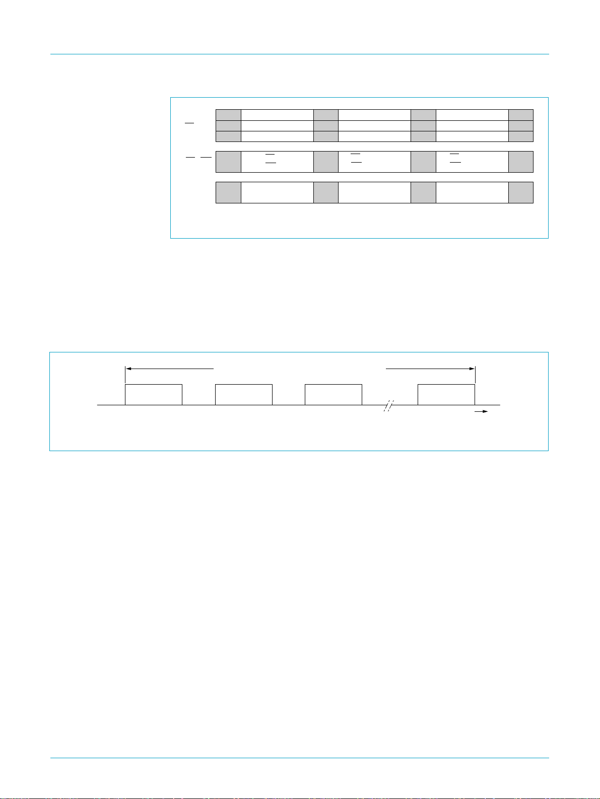
DREQ
ISP1161
Full-speed USB single-chip host and device controller
DACK
RD or WR
]
D[15:0
data #1 data #2 data #N
EOT
N = 1/2 byte count of transfer data.
Fig 18. DMA transfer for single-cycle burst mode.
DREQ
DACK
RD or WR
]
D[15:0
data #1 data #K data #2K data #Ndata #(K+1) data #(N−K+1)
MGT942
EOT
MGT943
N = 1/2 byte count of transfer data, K = number of cycles/burst.
Fig 19. DMA transfer for multi-cycle burst mode.
In both figures, the DMA transfer is configured such that DREQ is active HIGH and
DACK is active LOW.
9397 750 08313
Product data Rev. 01 — 3 July 2001 18 of 130
© Philips Electronics N.V. 2001. All rights reserved.

Philips Semiconductors
8.6 Interrupts
ISP1161 has separate interrupt request pins for the USB HC (INT1) and the USB DC
(INT2).
8.6.1 Pin configuration
The interrupt output signals have four configuration modes:
•
•
•
•
Figure 20 shows these four interrupt configuration modes. They are programmable
through register settings, which are also used to disable or enable the signals.
ISP1161
Full-speed USB single-chip host and device controller
Level trigger, active LOW
Level trigger, active HIGH
Edge trigger, active LOW
Edge trigger, active HIGH.
INT
(1) INT is level triggered, active LOW
INT
(2) INT is level triggered, active HIGH
INT
(3) INT is edge triggered, active LOW
INT
(4) INT is edge triggered, active HIGH
Fig 20. Interrupt pin operating modes.
8.6.2 HC’s interrupt output pin (INT1)
To program the four configuration modes of the HC’s interrupt output signal (INT1),
set bits 1 and 2 of the HcHardwareConfiguration register (20H - Read, A0H - Write).
Bit 0 is used as the master enable setting for pin INT1.
INT active
INT active
INT active
167 ns
INT active
167 ns
clear or disable INT
clear or disable INT
MGT944
INT1 has many interrupt events. The relationship between pin INT1 and its interrupt
events is shown as in Figure 21.
9397 750 08313
Product data Rev. 01 — 3 July 2001 19 of 130
© Philips Electronics N.V. 2001. All rights reserved.

Philips Semiconductors
ISP1161
Full-speed USB single-chip host and device controller
HcInterruptStatus
register
SO
SF
RD
UE
FNO
RHSC
SO IE
SF IE
RD IE
UE IE
FNO IE
RHSC IE
HcInterruptEnable
register
X
X
Fig 21. HC interrupt logic.
HcuPInterrupt
register
SOF/ITL
ATL
All EOT
OPR Reg
HcSuspend
ClkReady
PULSE
GENERATOR
1
0
INT1
MGT945
SOF/ITL IE
ATL IE
All EOT IE
OPR Reg IE
HcSuspend IE
ClkReady IE
HcuPInterruptEnable
register
INT Enable
INT Trigger
INT Polarity
.
.
.
HcHardwareConfiguration
register
The interrupt events of the HcµPInterrupt register (24H - Read, A4H - Write) changes
the status of pin INT1 when the corresponding bits of the HcµPInterruptEnable
register (25H - Read, A5H - Write) and pin INT1’s global enable bit (bit 0 of the
HcHardwareConfiguration register) are all set to enable status.
However, events that come from the HcInterruptStatus register (03H - Read, 83H Write) affect only the OPR_Reg bit of the HcµPInterrupt register. They cannot directly
change the status of pin INT1.
8.6.3 DC’s interrupt output pin (INT2)
The DC’s interrupt output pin INT2’s four configuration modes can also be
programmed by setting bit 0 (INTPOL) and bit 1 (INTLVL) of the DC’s hardware
configuration register (BBH - Read, BAH - Write). Bit 3 (INTENA) of the DC’s mode
register (B9H - Read, B8H - Write) is used as pin INT2’s global enable setting.
Figure 22 shows the relationship between the interrupt events and pin INT2.
Each of the indicated USB events is logged in a status bit of the Interrupt Register.
Corresponding bits in the Interrupt Enable Register determine whether or not an
event will generate an interrupt.
Interrupts can be masked globally by means of the INTENA bit of the Mode Register
(see Table 80).
The active level and signalling mode of the INT output is controlled by the INTPOL
and INTLVL bits of the Hardware Configuration Register (see Table 82). Default
settings after reset are active LOW and level mode. When pulse mode is selected, a
pulse of 166 ns is generated when the OR-ed combination of all interrupt bits
changes from logic 0 to logic 1.
9397 750 08313
Product data Rev. 01 — 3 July 2001 20 of 130
© Philips Electronics N.V. 2001. All rights reserved.

Philips Semiconductors
Bits RESET, RESUME, EOT and SOF are cleared upon reading the Interrupt
Register.The endpoint bits (EP0OUT to EP14) are cleared by reading the associated
Endpoint Status Register.
Bit BUSTATUS follows the USB bus status exactly, allowing the firmware to get the
current bus status when reading the Interrupt Register.
SETUP and OUT token interrupts are generated after ISP1161’s DC has
acknowledged the associated data packet. In bulk transfer mode, the ISP1161’s DC
will issue interrupts for every ACK received for an OUT token or transmitted for an IN
token.
In isochronous mode, an interrupt is issued upon each packet transaction. The
firmware must take care of timing synchronization with the host. This can be done via
the Pseudo Start-Of-Frame (PSOF) interrupt, enabled via bit IEPSOF in the Interrupt
Enable Register. If a Start-Of-Frame is lost, PSOF interrupts are generated every
1 ms. This allows the firmware to keep data transfer synchronized with the host. After
3 missed SOF events the ISP1161’s DC will enter ‘suspend’ state.
An alternative way of handling isochronous data transfer is to enable both the SOF
and the PSOF interrupts and disable the interrupt for each isochronous endpoint.
ISP1161
Full-speed USB single-chip host and device controller
DC Interrupt register
DC Interrupt Enable register
Fig 22. DC interrupt logic.
RESET
SUSPND
RESUME
SOF
EP14
...
EP0IN
EP0OUT
EOT
IERST
IESUSP
IERESM
IESOF
IEP14
...
IEP0IN
IEP0OUT
IEEOT
.
.
.
.
.
.
.
.
.
.
.
.
DC Device Mode register
INTENA
DC Hardware Configuration
register
INTLVL
INTPOL
PULSE
GENERATOR
1
0
INT2
MGT946
9397 750 08313
Product data Rev. 01 — 3 July 2001 21 of 130
© Philips Electronics N.V. 2001. All rights reserved.

Philips Semiconductors
9. The USB host controller (HC)
9.1 The HC’s four USB states
ISP1161’s USB HC has four USB states−USB Operational, USB Reset, USB
Suspend, and USB Resume− that define the HC’s USB signaling and bus states
responsibilities. The signals are visible to the HC (software) Driver via ISP1161 USB
HC’s control registers.
ISP1161
Full-speed USB single-chip host and device controller
USB_OPERATIONAL write
USB_SUSPEND write
Fig 23. ISP1161 HC’s USB states.
The USB states are reflected in the HostControllerFunctionalState field of the
HcControl register (01H - Read, 81H - Write), which is located at bits 7 and 6 of the
register.
USB_OPERATIONAL
USB_SUSPEND
software reset
USB_OPERATIONAL write
USB_RESUME
USB_RESUME write
or
remote wake-up
USB_RESET write
USB_RESET write
USB_RESET write
USB_RESET
hardware reset
MGT947
The HC Driver can perform only the USB state transitions shown in Figure 23.
Remark: The Software Reset in Figure 23 is not caused by the HcSoftwareReset
command. It is caused by the HostControllerReset field of the HcCommandStatus
register (02H - Read, 82H - Write).
9.2 Generating USB traffic
USB traffic can be generated only when the ISP1161 USB HC is under the USB
Operational State. Therefore, the HC Driver must set the
HostControllerFunctionalState field of the HcControl register before generating USB
traffic.
9397 750 08313
Product data Rev. 01 — 3 July 2001 22 of 130
© Philips Electronics N.V. 2001. All rights reserved.

Philips Semiconductors
A simplistic flow diagram showing when and how to generate USB traffic is shown in
Figure 24. For greater accuracy, refer to both the
Revision 1.1
ISP1161
Full-speed USB single-chip host and device controller
Universal Serial Bus Specification
about the protocol and ISP1161 USB HC’s register usage.
Reset
HC state =
Initialize
HC
Entry
Fig 24. ISP1161 HC operating flow.
USB_Operational
Reset
•
This includes hardware reset by pin RESET and software reset by the
HcSoftwareReset command (A9H). The reset function will clear all the HC’s
internal control registers to their reset status. After reset, the HC Driver must
initialize the ISP1161 USB HC by setting some registers.
Initialize HC
•
It includes:
– Setting the physical size for the HC’s internal FIFO buffer RAM by setting the
HcITLBufferLength register (2AH - Read, AAH - Write) and the
HcATLBufferLength register (2BH - Read, ABH - Write)
– Setting the HcHardwareConfiguration register according to requirements
– Clearing interrupt events, if required
– Enabling interrupt events, if required
– Setting the HcFmInterval register (0DH - Read, 8DH - Write)
– Setting the HC’s root hub registers
– Setting the HcControl register to move the HC into USB Operational state
See also Section 9.5.
Entry
•
The normal entry point. The microprocessor returns to this point when there are
HC requests.
Need USB Traffic
•
USB devices need the HC to generate USB traffic when they have USB traffic
requests such as:
– Connecting to or disconnecting from the downstream ports
– Issuing the Resume signal to the HC
To generate USB traffic, the HC Driver must enter the USB transaction loop.
Exit
no
Need
USB traffic?
HC informs HCD of
USB traffic results
yes
Prepare PTD data in
µP system RAM
HC performs USB transactions
via USB bus I/F
Transfer PTD data into
HC FIFO buffer RAM
HC interprets
PTD data
MGT948
9397 750 08313
Product data Rev. 01 — 3 July 2001 23 of 130
© Philips Electronics N.V. 2001. All rights reserved.

Philips Semiconductors
•
•
•
•
•
ISP1161
Full-speed USB single-chip host and device controller
Prepare PTD Data in µP System RAM
The communication channel between the HC Driver and ISP1161’s USB HC is in
the form of Philips Transfer Descriptor (PTD) data. The PTD data provides USB
traffic information about the commands, status, and USB data packets.
The physical storage media of PTD data for the HC Driver is the microprocessor’s
system RAM. For ISP1161’s USB HC, it is the ISP1161’s internal FIFO buffer
RAM.
The HC Driver prepares PTD data in the microprocessor’s system RAM for transfer
to ISP1161’s HC internal FIFO buffer RAM.
Transfer PTD Data into HC’s FIFO Buffer RAM
When PTD data is ready in the microprocessor’s system RAM, the HC Driver must
transfer the PTD data from the microprocessor’s system RAM into ISP1161’s
internal FIFO buffer RAM.
HC Interprets PTD Data
The HC determines what USB transactions are required based on the PTD data
that have been transferred into the internal FIFO buffer RAM.
HC Performs USB Transactions via USB Bus Interface
The HC performs the USB transactions with the specified USB device endpoint
through the USB bus interface.
HC Informs HCD the USB Traffic Results
The USB transaction status and the feedback from the specified USB device
endpoint will be put back into the ISP1161’s HC internal FIFO buffer RAM in PTD
data format. The HC Driver can read back the PTD data from the internal FIFO
buffer RAM.
9.3 PTD data structure
The Philips Transfer Descriptor (PTD) data structure provides a communication
channel between the HC Driver and the ISP1161’s USB HC. PTD data contains
information required by the USB traffic. PTD data consists of a PTD followed by its
payload data, as shown in Figure 25.
top
bottom
Fig 25. PTD data in FIFO buffer RAM.
FIFO buffer RAM
PTD
payload data
PTD
payload data
PTD
payload data
PTD data #1
PTD data #2
PTD data #N
MGT949
9397 750 08313
Product data Rev. 01 — 3 July 2001 24 of 130
© Philips Electronics N.V. 2001. All rights reserved.

Philips Semiconductors
ISP1161
Full-speed USB single-chip host and device controller
The PTD data structure is used by the HC to define a bufferof data that will be moved
to or from an endpoint in the USB device. This data buffer is set up for the current
frame (1 ms frame) by the firmware, the HC Driver. The payload data for every
transfer in the frame must have a PTD as a header to describe the characteristic of
the transfer. PTD data is DWORD aligned.
9.3.1 PTD data header definition
The PTD forms the header of the PTD data. It tells the HC the transfer type, where
the payload data should go, and the payload data’s actual size. A PTD is an 8-byte
data structure that is very important for HC Driver programming.
Table 4: Philips Transfer Descriptor (PTD): bit allocation
Bit 7 6 5 4 3 2 1 0
Byte 0 ActualBytes[7:0]
Byte 1 CompletionCode[3:0] Active Toggle ActualBytes[9:8]
Byte 2 MaxPacketSize[7:0]
Byte 3 EndpointNumber[3:0] Last Speed MaxPacketSize[9:8]
Byte 4 TotalBytes[7:0]
Byte 5 DirectionPID[1:0] TotalBytes[9:8]
Byte 6 Format FunctionAddress[6:0]
Byte 7
9397 750 08313
Product data Rev. 01 — 3 July 2001 25 of 130
© Philips Electronics N.V. 2001. All rights reserved.

Philips Semiconductors
ISP1161
Full-speed USB single-chip host and device controller
Table 5: Philips Transfer Descriptor (PTD): bit description
Symbol Access Description
ActualBytes[9:0] R/W Contains the number of bytes that were transferred for this PTD
CompletionCode[3:0] R/W 0000 NoError General TD or isochronous data packet processing
completed with no detected errors.
0001 CRC Last data packet from endpoint contained a CRC error.
0010 BitStuffing Last data packet from endpoint contained a bit stuffing
violation.
0011 DataToggleMismatch Last packet from endpoint had data toggle PID that did
not match the expected value.
0100 Stall TD was moved to the Done queue because the
endpoint returned a STALL PID.
0101 DeviceNotResponding Devicedid not respond to token (IN) or did not provide a
handshake (OUT).
0110 PIDCheckFailure Check bits on PID from endpoint failed on data PID (IN)
or handshake (OUT)
0111 UnexpectedPID Received PID was not valid when encountered or PID
value is not defined.
1000 DataOverrun The amount of data returned by the endpoint exceeded
either the size of the maximum data packet allowed
from the endpoint (foundin MaximumPacketSize field of
ED) or the remaining buffer size.
1001 DataUnderrun The endpoint returned is less than MaximumPacketSize
and that amount was not sufficient to fill the specified
buffer.
1010 reserved 1011 reserved 1100 BufferOverrun During an IN, the HC received data from an endpoint
faster than it could be written to system memory.
1101 BufferUnderrun During an OUT, the HC could not retrieve data from the
system memory fast enough to keep up with the USB
data rate.
Active R/W Set to logic 1 by firmware to enable the execution of transactions by the HC. When the
transaction associated with this descriptor is completed, the HC sets this bit to logic 0,
indicating that a transaction for this element should not be executed when it is next
encountered in the schedule.
Toggle R/W Used to generate or compare the data PID value (DATA0 or DATA1). It is updated after
each successful transmission or reception of a data packet.
MaxPacketSize[9:0] R The maximum number of bytes that can be sent to or received from the endpoint in a
single data packet.
EndpointNumber[3:0] R USB address of the endpoint within the function.
Last(PTD) R Last PTD of a list (ITL or ATL). A logic 1 indicates that the PTD is the last PTD.
(Low)Speed R Speed of the endpoint:
S = 0 — full speed
S = 1 — low speed
9397 750 08313
Product data Rev. 01 — 3 July 2001 26 of 130
© Philips Electronics N.V. 2001. All rights reserved.

Philips Semiconductors
ISP1161
Full-speed USB single-chip host and device controller
Table 5: Philips Transfer Descriptor (PTD): bit description
Symbol Access Description
TotalBytes[9:0] R Specifies the total number of bytes to be transferred with this data structure.ForBulk and
Control only, this can be greater than MaximumPacketSize.
DirectionPID[1:0] R 00 SETUP
01 OUT
10 IN
11 reserved
Format R The format of this data structure. If this is a Control, Bulk or Interrupt endpoint, then
Format = 0. If this is an Isochronous endpoint, then Format = 1.
FunctionAddress[6:0] R The is the USB address of the function containing the endpoint that this PTD refers to.
…continued
9.4 HC’s internal FIFO buffer RAM structure
9.4.1 Partitions
According to the
USB data transfers: Control, Bulk, Interrupt and Isochronous.
The HC’s internal FIFO buffer RAM is of a physical size of 4 kbytes. This internal
FIFO buffer RAM is used for transferring data between the microprocessor and USB
peripheral devices. This on-chip buffer RAM can be partitioned into two areas:
Acknowledged Transfer List (ATL) buffer and Isochronous (ISO)Transfer List (ITL)
buffer. The ITL buffer is a Ping-pong structured FIFO buffer RAM that is used to keep
the payload data and their PTD header for Isochronous transfers. The ATL buffer is a
non Ping-pong structured FIFO buffer RAM that is used for the other three types of
transfers.
Universal Serial Bus Specification Rev 1.1
, there are four types of
For the ITL buffer, it can be further partitioned into ITL0 and ITL1 for the Ping-Pong
structure. The ITL0 buffer and ITL1 buffer always have the same size. The
microprocessor can put ISO data into either the ITL0 buffer or the ITL1 buffer. When
the microprocessor accesses an ITL buffer, the HC can take over another ITL buffer
at the same time. This architecture can improve the ISO transfer performance.
The Host Controller Driver can assign the logical size for ATL buffer and ITL buffers at
any time, but normally at initialization after power-on reset, by setting the
HcATLBufferLength register (2BH - Read, ABH - Write) and HcITLBufferLength
register (2AH - Read, AAH - Write), respectively. However, the total length (ATL buffer
+ ITL buffer) should not exceed 4 kbytes, the maximum RAM size. Figure 26 shows
the partitions of the internal FIFO buffer RAM. When assigning buffer RAM sizes,
follow this formula:
ATL buffer length + 2 × (ITL buffer size) ≤ 1000H (that is, 4 kbytes)
where: ITL buffer size = ITL0 buffer length = ITL1 buffer length
The following assignments are examples of legal uses of the internal FIFO buffer
RAM:
ATL buffer length = 800H, ITL buffer length = 400H.
•
This is the maximum use of the internal FIFO buffer RAM.
9397 750 08313
Product data Rev. 01 — 3 July 2001 27 of 130
© Philips Electronics N.V. 2001. All rights reserved.

Philips Semiconductors
•
•
•
Full-speed USB single-chip host and device controller
ATL buffer length = 400H, ITL buffer length = 200H.
This is insufficient use of the internal FIFO buffer RAM.
ATL buffer length = 1000H, ITL buffer length = 0H.
This will use the internal FIFO buffer RAM for only ATL transfers.
ATL buffer length = 0H, ITL buffer length = 800H.
This will use the internal FIFO buffer RAM for only ISO transfers.
FIFO buffer RAM
top
ITL0
ITL buffer
ITL1
ISO data A
ISO data B
programmable
sizes
ISP1161
ATL buffer
Fig 26. HC Internal FIFO buffer RAM partitions.
ATL
bottom
control/bulk/interrupt
data
not used
MGT950
4 kbytes
The actual requirement for the buffer RAM may not reach the maximum size. You can
make your selection based on your application.
The following are some calculations of the ISO_A or ISO_B space for a frame of data:
Maximum number of useful data sent during one USB frame is 1280 bytes (20 ISO
packets of 64 bytes). Total RAM size needed for this is 20 × 8 + 1280 = 1440 bytes.
Maximum number of packets for different endpoints sent during one USB frame is
•
150 (150 ISO packets of 1 byte). Total RAM size needed is
150 × 8 + 150 × 1 = 1350 bytes.
The Ping buffer RAM (ITL0) and the Pong buffer RAM (ITL1) have a maximum size
•
of 2 kbytes each. All data needed for one frame can be stored in the Ping or the
Pong buffer RAM.
When the embedded system wants to initiate a transfer to the USB bus, the data
needed for one frame is transferred to the ATL buffer or ITL buffer. The
microprocessor detects the buffer status through the interrupt routines. When the
HcBufferStatus register (2CH - Read only) indicates that buffer is empty, then the
microprocessor can write data into the buffer. When the HcBufferStatus register
indicates that buffer is full, that is data is ready on the buffer, the microprocessor
needs to read data from the buffer.
During every 1 ms, there might be many events to generate interrupt requests to the
microprocessor for data transfer or status retrieval. However, each of the interrupt
types defined in this specification can be enabled or disabled by setting the
HcµPInterruptEnable register bits accordingly.
9397 750 08313
Product data Rev. 01 — 3 July 2001 28 of 130
© Philips Electronics N.V. 2001. All rights reserved.

Philips Semiconductors
The data transfer can be done via PIO mode or DMA mode. The data transfer rate
can go up to 15 Mbyte/s. In DMA operation, single-cycle or multi-cycle burst modes
are supported. For the multi-cycle burst mode, 1, 4, or 8 cycles per burst is supported
for ISP1161.
9.4.2 Data organization
PTD data is used for every data transfer between a microprocessor and the USB bus,
and the PTD data resides in the buffer RAM. For an OUT or SETUP transfer, the
payload data is placed just after the PTD, after which the next PTD is placed. For an
IN transfer,some RAM space is reservedforreceiving a number of bytes that is equal
to the total bytes of the transfer. After this, the next PTD and its payload data are
placed (see Figure 27).
Remark: The PTD is defined for both ATL and ITL type data transfer. For ITL, the
PTD data should be put into ITL buffer RAM, the ISP1161 takes care of the
Ping-Pong action for the ITL buffer RAM access.
ISP1161
Full-speed USB single-chip host and device controller
RAM buffer
top
PTD of OUT transfer
000H
payload data of OUT transfer
PTD of IN transfer
empty space for IN total data
PTD of OUT transfer
payload data of OUT transfer
bottom
Fig 27. Buffer RAM data organization.
7FFH
MGT952
The PTD data (PTD header and its payload data) is a structure of DWORD (doubleword or 4-byte) alignment. This means that the memory address is organized in steps
of 4 bytes. Therefore, the first byte of every PTD and the first byte of every payload
data are located at an address which is a multiple of 4. Figure 28 illustrates an
example in which the first payload data is 14 bytes long, meaning that the last byte of
the payload data is at the location 15H. The next addresses (16H and 17H) are not
multiples of 4. Therefore, the first byte of the next PTD will be located at the next
multiple-of-four address, 18H.
9397 750 08313
Product data Rev. 01 — 3 July 2001 29 of 130
© Philips Electronics N.V. 2001. All rights reserved.

Philips Semiconductors
ISP1161
Full-speed USB single-chip host and device controller
RAM buffer
PTD
(8 bytes)
payload data
(14 bytes)
PTD
(8 bytes)
payload data
00Htop
08H
15H
18H
20H
MGT953
Fig 28. PTD data with DWORD alignment in buffer RAM.
9.4.3 Operation & C Program Example
Figure 29 shows the block diagram for internal FIFO buffer RAM operations by PIO
mode. ISP1161 provides one register as the access port for each buffer RAM. For the
ITL buffer RAM, the access port is the ITLBufferPort register (40H - Read, C0H Write). For the ATL buffer RAM, the access port is the ATLBufferPort register (41H Read, C1H - Write). The buffer RAM is an array of bytes (8 bits) while the access port
is a 16-bit register. Therefore, each read/write operation on the port accesses two
consecutive memory locations, incrementing the pointer of the internal buffer RAM by
two.
The lower byte of the access port register corresponds to the data byte at the even
location of the buffer RAM, and the higher byte in the access port register
corresponds to the other data byte at the odd location of the buffer RAM. Regardless
of the number of data bytes to be transferred, the command code must be issued
merely once, and it will be followed by a number of accesses of the data port (see
Section 8.4).
When the pointer of the buffer RAM reaches the value of the HcTransferCounter
register, an internal EOT signal will be generated to set bit 2, AllEOTInterrupt, of the
HcµPinterrupt register and update the HcBufferStatus register, to indicate that the
whole data transfer has been completed.
For ITL buffer RAM, every start of frame (SOF) signal (1 ms) will cause toggling
between ITL0 and ITL1 but this depends on the buffer status. If both ITL0BufferFull
and ITL1BufferFull of the HcBufferStatus register are already logic 1, meaning that
both ITL0 and ITL1 buffer RAMs are full, the toggling will not happen. In this case, the
microprocessor will always have access to ITL1.
9397 750 08313
Product data Rev. 01 — 3 July 2001 30 of 130
© Philips Electronics N.V. 2001. All rights reserved.
 Loading...