

Page 1

ISP1109
Universal Serial Bus transceiver with carkit support
Rev. 01 — 14 July 2005 Product data sheet
1. General description
The ISP1109 is a Universal Serial Bus (USB) transceiver device that supports
CEA−936−A, Mini-USB Analog Carkit Interface
Bus SpecificationRev. 2.0
(12 Mbit/s) and low-speed (1.5 Mbit/s) data rates.
The ISP1109 is available in HVQFN32 package.
2. Features
. It is fully compliant with
. TheISP1109 can transmit and receiveserial data at full-speed
Universal Serial
■ Fully complies with
■ Supports
■ Can transmit and receive serial data at full-speed (12 Mbit/s) and low-speed
■ Supports Serial Parallel Interface (SPI) (up to 26 MHz) and I2C-bus (up to 400 kHz)
■ Supports Universal Asynchronous Receiver-Transmitter (UART) pass-through on the
■ Built-in analog switches to support analog audio signals multiplexedon the DP and DM
■ Supports On-The-Go (OTG) Session Request Protocol (SRP)
■ Supports Power-down mode, in which the whole chip consumes less than 20 µA
■ 3.0 V to 5.25 V power supply input range (VCC)
■ Supports wide range digital interfacing I/O voltage (V
■ ±12 kV ESD protection at pins DP, DM, ID, V
■ Supports charger current switching (ISET) detection
■ Full industrial grade operation from −40 °Cto+85°C
■ Available in a small HVQFN32 (5 x 5 mm2) halogen-free and lead-free package.
3. Applications
Universal Serial Bus Specification Rev. 2.0
CEA−936−A, Mini-USB Analog Carkit Interface
(1.5 Mbit/s) data rates
serial interface to access control and status registers
DP and DM lines
lines
power current
, VCC, GNDA and GNDD
BUS
) of 1.65 V to 3.6 V
CC(I/O)
■ Mobile phones.
Page 2

Philips Semiconductors
USB transceiver with carkit support
4. Ordering information
Table 1: Ordering information
Type number Package
Name Description Version
ISP1109BS HVQFN32 plastic thermal enhanced very thin quad flat package; no leads;
32 terminals; body 5x5x0.85 mm
ISP1109
SOT617-1
9397 750 13355 © Koninklijke Philips Electronics N.V. 2005. All rights reserved.
Product data sheet Rev. 01 — 14 July 2005 2 of 59
Page 3
Philips Semiconductors
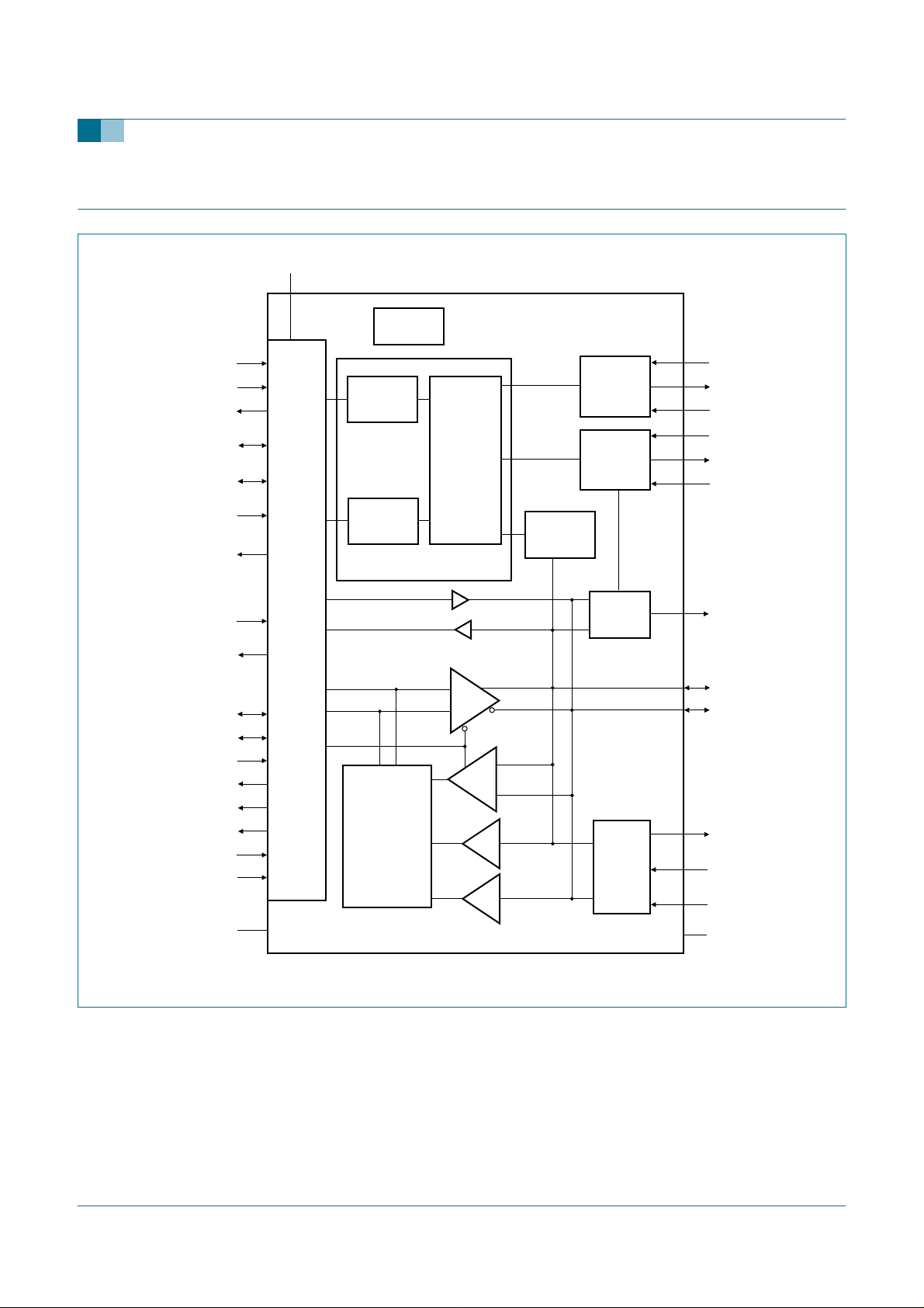
5. Block diagram
V
CC(I/O)
RESET_N
SPI_I2C_SEL
SPI_MISO
SPI_MOSI/
I2C_SDA
SPI_CLK/
I2C_SCL
SPI_CS/
I2C_ADR
INT_N
UART_TXD
5
9
10
11
12
13
4
SHIFTER
25
8, 19
LEVEL
CLOCK AND
TIMER
SPI
INTERFACE
REGISTERS
I2C-BUS
INTERFACE
SERIAL CONTROLLER
ISP1109
DP_PU/
DP_INT
DETECTOR
ISP1109
USB transceiver with carkit support
POWER
BLOCK
ID DET
ISET
CONTROL
3
21
30
31
28
29
27
V
CC
REG3V3
V
BUS
V
REF
ID_PU
ID
ISET
UART_RXD
DAT/VP
SE0/VM
OE_N
RCV
VP
VM
SPEED
SUSPEND
GNDD
Fig 1. Block diagram.
26
18
17
20
16
15
14
6
7
die pad
SE DETECTOR
DIF TX
DIF RX
SE
D+
SE
D−
23
22
+
−
32
AUDIO
SWITCH
1
2
24
004aaa486
DP
DM
MIC
SPKR_R
SPKR_L
GNDA
9397 750 13355 © Koninklijke Philips Electronics N.V. 2005. All rights reserved.
Product data sheet Rev. 01 — 14 July 2005 3 of 59
Page 4
Philips Semiconductors
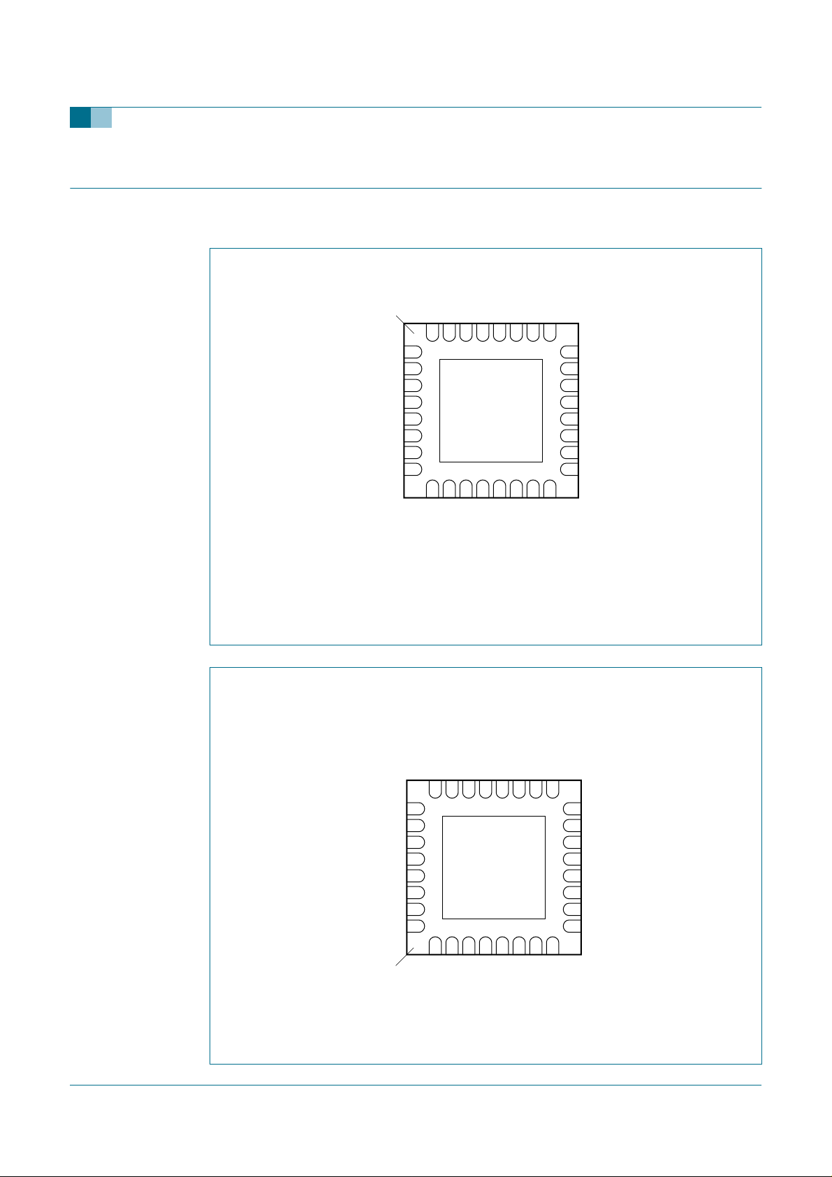
6. Pinning information
6.1 Pinning
ISP1109
USB transceiver with carkit support
terminal 1
index area
SPKR_R GNDA
SPKR_L DP
RESET_N OE_N
SPEED V
SUSPEND
V
1 24
2 23
3 22
V
CC
4 21
INT_N REG3V3
5 20
6 19
7 18
8 17
CC(I/O)
REFVBUS
MIC
V
32313029282726
ISP1109BS
9
10111213141516
SPI_MISO
SPI_I2C_SEL
SPI_MOSI/I2C_SDA
Transparent top view
Fig 2. Pin configuration HVQFN32; top view.
ID
ID_PU
ISET
UART_RXD
UART_TXD
25
VP
VM
RCV
SPI_CS/I2C_ADR
SPI_CLK/I2C_SCL
DM
CC(I/O)
DAT/VP
SE0/VM
004aaa487
SPI_I2C_SEL
SPI_MISO
SPI_MOSI/I2C_SDA
SPI_CLK/I2C_SCL
SPI_CS/I2C_ADR
VMVPRCV
9
10111213141516
V
SUSPEND DAT/VP
SPEED V
RESET_N OE_N
SPKR_L
SPKR_R
terminal 1
index area
8 17
CC(I/O)
7 18
6 19
5 20
4 21
INT_N REG3V3
3 22
V
CC
2 23
1 24
GNDD
(exposed die pad)
ISP1109BS
32313029282726
ID
REF
BUS
MIC
V
V
Bottom view
ISET
ID_PU
UART_RXD
SE0/VM
CC(I/O)
DM
DP
GNDA
25
004aaa703
UART_TXD
Fig 3. Pin configuration HVQFN32; bottom view.
9397 750 13355 © Koninklijke Philips Electronics N.V. 2005. All rights reserved.
Product data sheet Rev. 01 — 14 July 2005 4 of 59
Page 5

Philips Semiconductors
6.2 Pin description
Table 2: Pin description
Symbol
SPKR_R 1 AI - analog audio input signal for the right speaker
SPKR_L 2 AI - analog audio input signal for the left speaker
V
CC
INT_N 4 OD high-Z interrupt output; active LOW; connect to V
RESET_N 5 I - asynchronous reset input, active LOW
SPEED 6 I - speed selection input for the USB transceiver:
SUSPEND 7 I - suspend selection input for the USB transceiver:
V
CC(I/O)
SPI_I2C_
SEL
SPI_MISO 10 O - SPI slave data output; leave this pin open when
SPI_MOSI/
I2C_SDA
USB transceiver with carkit support
[1] [2]
Pin Type
3 P - supply voltage; operates when
[3]
Reset
state
Description
channel
channel
3.0 V < V
< 5.25 V
CC
through a 3.3 kΩ resistor
open-drain output
input
• LOW: USB low-speed
• HIGH: USB full-speed.
when not in use, connect to V
10 kΩ resistor
input
• LOW: normal operation
• HIGH: suspend mode.
when not in use, connect to ground through a
10 kΩ resistor
input
8 P - supply voltage for I/O interface logic signals
(1.65 V to 3.6 V)
2
9 I - selection of SPI or I
C-bus serial interface to
access internal registers:
• LOW: SPI slave interface is selected
• HIGH: I
The I
is determined by pin 13 (I2C_ADR).
input
2
C-bus is selected
I
push-pull output
11 I/OD high-Z SPI_MOSI input — SPI slave data input
I2C_SDA input and output — serial I
when used as an I
open-drain; connect to V
resistor.
2
C-bus slave interface is selected.
2
C-bus device address is 010 110Xb; here X
2
C-bus data, the pad is
CC(I/O)
ISP1109
CC(I/O)
through a
CC(I/O)
2
C-bus data;
through a 3.3 kΩ
9397 750 13355 © Koninklijke Philips Electronics N.V. 2005. All rights reserved.
Product data sheet Rev. 01 — 14 July 2005 5 of 59
Page 6

Philips Semiconductors
ISP1109
USB transceiver with carkit support
Table 2: Pin description
CC(I/O)
[1] [2]
Pin Type
12 I/OD high-Z SPI_CLK input — SPI clock input
13 I - SPI_CS input — SPI chip select input
19 P - supply voltage for the I/O interface logic signals
Symbol
SPI_CLK/
I2C_SCL
SPI_CS/
I2C_ADR
VM 14 O - single-ended DM receiver output; leave this pin
VP 15 O - single-ended DP receiver output; leave this pin
RCV 16 O 0 differential receiver output; leave this pin open
SE0/VM 17 I/O high-Z SE0 input and output — SE0 functions in
DAT/VP 18 I/O high-Z DAT input and output — DAT functions in
V
OE_N 20 I - enable differential transmitter input
REG3V3 21 P - regulated output voltage 3.3 V; a 0.1 µF external
DM 22 AI/O high-Z this pin can be programmed as:
…continued
[3]
Reset
state
Description
2
I2C_SCL input and output — serial I
when used as an I
open-drain; connect to V
resistor.
I2C_ADR input — LSB address offset of the
2
I
C-bus slave address.
input
open when not in use
push-pull output
open when not in use
push-pull output
when not in use
push-pull output
DAT_SE0 USB mode
VM input and output — VM functions in VP_VM
USB mode.
bidirectional pad
DAT_SE0 USB mode
VP input and output — VP functions in VP_VM
USB mode.
bidirectional pad
(1.65 V to 3.6 V)
input
capacitor is required
2
C-bus clock, the pad is
through a 3.3 kΩ
CC(I/O)
C-busclock;
• USB D− (data minus pin)
• transparent UART RxD or
• transparent audio SPKR_L.
DP 23 AI/O high-Z this pin can be programmed as:
• USB D+ (data plus pin)
• transparent UART TxD or
• transparent audio SPKR_R or MIC.
GNDA 24 P - analog ground
9397 750 13355 © Koninklijke Philips Electronics N.V. 2005. All rights reserved.
Product data sheet Rev. 01 — 14 July 2005 6 of 59
Page 7

Philips Semiconductors
ISP1109
USB transceiver with carkit support
Table 2: Pin description
Symbol
[1] [2]
Pin Type
…continued
[3]
Reset
Description
state
UART_TXD 25 I - connect to TxD of the UART controller; when not in
use, connect to V
through a 10 kΩ resistor
CC(I/O)
input
UART_RXD 26 O - connect to RxD of the UART controller; leave this
pin open when not in use
push-pull output
ISET 27 O
[4]
- output indicating detection of the carkit, charger or
factory mode to enable high current mode of the
phone charger; leave this pin open when not in use
push-pull output
ID_PU 28 AI - an external resistor is connected between the ID
and ID_PU pins
ID 29 AI - identification detector input of the USB mini
connector
V
BUS
V
REF
30 AI - V
line input supply voltage of the USB
BUS
connector
[5]
31 P - supply voltage for audio circuits; 2.775 V ± 0.1 V
MIC 32 AO - audio output signal for the microphone channel
GNDD exposed
P - digital ground
die pad
[1] Symbol names ending with underscore N—for example, NAME_N—indicate active LOW signals.
[2] Use a decoupling capacitor of 0.1 µF on all V
[3] I = input; O = output; I/O = digital input/output; OD = open-drain output; AI/O = analog input/output;
P = power or ground.
[4] The ISET pin is powered by REG3V3. All other digital pins are powered by V
[5] For the decoupling capacitor requirement, refer to Table 7-7 of
CC(I/O)
, V
and VCC pins.
REF
.
CC(I/O)
Universal Serial Bus Specification Rev. 2.0
.
9397 750 13355 © Koninklijke Philips Electronics N.V. 2005. All rights reserved.
Product data sheet Rev. 01 — 14 July 2005 7 of 59
Page 8

Philips Semiconductors
7. Functional description
7.1 Serial controller
The serial controller includes the following functions:
ISP1109
USB transceiver with carkit support
• Serial Controller interface (SPI or I
2
C-bus)
• Device Identification registers
• Control registers
• Interrupt registers
• Interrupt generator.
The serial controller acts as an SPI slave or I2C-bus slave.
All the registers are the same as that in SPI or I2C-bus mode. In I2C-bus mode, the
registers are accessed in 8-bit width (bits 0 to 7) for each address. In SPI mode, there are
25 bits for each address, only bits 0 to 7 are useful while bits 8 to 24 are don’t cares.
At hardware reset including power-on reset, the level on pin SPI_I2C_SEL will determine
whether the SPI or I2C-bus interface is active. If SPI_I2C_SEL = LOW, the SPI interface is
selected. If SPI_I2C_SEL = HIGH, the I2C-bus interface is selected.
7.2 V
detector
BUS
The V
session valid comparator threshold voltage (V
bit VBUS_DET of the Interrupt Source register. If V
stored.
detector provides voltage level detection on V
BUS
th(svc)
. If V
BUS
), logic 1 will be stored in
is below V
BUS
is above the V
BUS
, logic 0 will be
th(svc)
BUS
7.3 ID detector
In normal power mode, that is, when both VCC and V
senses the condition of the ID line and can differentiate between the following three
conditions:
are present, the ID detector
CC(I/O)
• ID pin is floating (bit ID_FLOAT = 1)
• ID pin is shorted to ground (bit ID_GND = 1)
• ID pin is connected to ground through resistor R
are logic 0).
The recommended procedure to detect the status of ID using software is:
1. When nothing is connected, ID is in the ID_FLOAT state. Enable the ID_FLOAT
interrupt (falling edge).
2. If an interrupt occurs, read the Interrupt Latch register. If ID changes, bit ID_FLOAT is
set.
3. The software waits for sometime, for example: 100 ms, to allow mechanical
debounce.
4. The software reads the Interrupt Source register, and checks bits ID_FLOAT and
ID_GND.
9397 750 13355 © Koninklijke Philips Electronics N.V. 2005. All rights reserved.
Product data sheet Rev. 01 — 14 July 2005 8 of 59
(bits ID_FLOAT and ID_GND
DN(ID)
Page 9

Philips Semiconductors
The ID detector has a switch that can be used to ground pin ID. This switch is controlled
by bit ID_PULLDN of the Resistor Control register, and bits PH_ID_INT and PH_ID_ACK
of the Audio Control register. See Table 3.
Table 3: ID pull-down control
ID_PULLDN PH_ID_ACK PH_ID_INT Switch between ID and GND
000off
0 0 1 on for time t
010waitfortime t
0 1 1 not defined
1XXon
USB transceiver with carkit support
then off; bit PH_ID_INT
auto-clears to 0
off; bit PH_ID_ACK auto-clears to 0
Wint(ID)
, turn on the switch for t
int(ID)
ISP1109
then
Wint(ID)
The ID detector also has a switch that is connected between the ID_PU and V
the voltage on the ID pin is higher than the voltage on the V
pin, the switch will be
REF
REF
turned off. Otherwise, the switch will remain on.
7.4 Pull-up and pull-down resistors
The DP pull-up resistor can be enabled or disabled (default enabled) using register
bit DP_PULLUP, if V
be enabled, if VCC>V
To support DP Session Request Protocol (SRP), it is required that a B-device can perform
DP pulsing when V
bit DP_SRP_EN is set, the DP pull-up resistor will be enabled irrespective of the status of
V
.
BUS
Table 4: DP pull-up resistor (R
Bit V
DP_SRP_EN DP_PULLUP V
00XXXoff
0 1 no X X off
01XLOWXoff
0 1 X X LOW off
0 1 yes HIGH HIGH on
1 X X X HIGH on
) control
UP(DP)
BUS>Vth(svc)
is above V
BUS
and V
th(ISET)
is below the session end threshold (0.2 V to 0.8 V). If register
BUS
Pin DP pull-up resistor (SW1)
CC(I/O)
. The pull-up resistance on pin DP (R
th(svc)
BUS>Vth(svc)
HIGH RESET_N
.
UP(DP)
pins. If
) must
The pull-up resistor is context variable, as described in document
ECN_27%_Resistor
.
The value of the pull-up resistor depends on the condition of the USB bus:
• When the bus is idle, the value of the resistor is 900 Ω to 1575 Ω (SW2 = on).
• When the bus is transmitting or receiving, the value of the resistor is 1425 Ω to
3090 Ω (SW2 = off).
DP also implements a weak pull-up resistor (R
weakUP(DP)
bit DP_WKPU_EN of the Resistor Control register; see Figure 4. R
connected to the DP pin (SW3 = on), if bit DP_WKPU_EN = 1 and the voltage on V
greater than V
9397 750 13355 © Koninklijke Philips Electronics N.V. 2005. All rights reserved.
Product data sheet Rev. 01 — 14 July 2005 9 of 59
th(svc)
.
) that is controlled by
weakUP(DP)
will be
BUS
is
Page 10
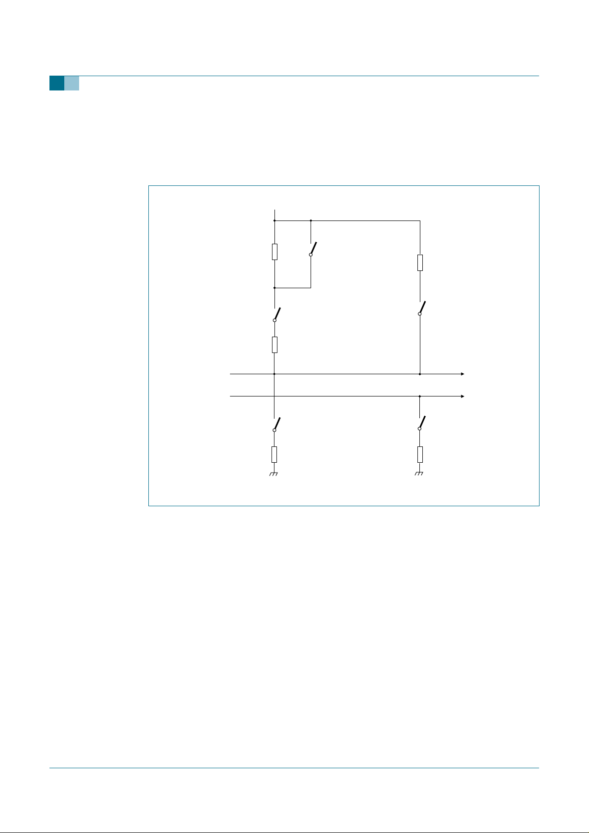
Philips Semiconductors
ISP1109
USB transceiver with carkit support
The DP pull-down resistor (R
) is connected to the DP line, if bit DP_PULLDOWN in
DN(DP)
the Resistor Control register is set.
The DM pull-down resistor (R
DN(DM)
in the Resistor Control register is set.
REG3V3
0.525 kΩ to
1.515 kΩ
SW1
0.9 kΩ to
1.575 kΩ
DP
DM
) is connected to the DM line, if bit DM_PULLDOWN
SW2
R
weakUP(DP)
130 kΩ ± 30 %
SW3
DM_PULLDOWN
15 kΩ
(14.3 kΩ to
24.8 kΩ)
004aaa520
15 kΩ
(14.3 kΩ to
24.8 kΩ)
DP_PULLDOWN
R
DN(DP)
R
DN(DM)
Fig 4. DP and DM pull-up and pull-down resistors.
7.5 Power block
The built-in DC-DC regulator conditions the input power supply (VCC) for use in the core of
the ISP1109.
When VCC is greater than 3.6 V, the regulator will output 3.3 V ± 10 %. When VCC is less
than 3.6 V, the regulator will be bypassed and pin REG3V3 will be shorted to pin VCC.
The output of the regulator can be monitored on pin REG3V3. A capacitor (0.1 µF) will be
connected to pin REG3V3.
7.6 Carkit DP interrupt detector
The carkit DP interrupt detector is a comparator that detects the carkit interrupt signal on
the DP line in analog audio mode. Bit DP_INT will be cleared (set to logic 0), if the voltage
level on the DP line is below the carkit interrupt threshold V
thPH(DP)L
(0.4 V to 0.6 V).
The carkit interrupt detector is enabled in audio mode only (bit AUDIO_EN = 1).
9397 750 13355 © Koninklijke Philips Electronics N.V. 2005. All rights reserved.
Product data sheet Rev. 01 — 14 July 2005 10 of 59
Page 11

Philips Semiconductors
7.7 Audio switches
The audio switchesprovide low impedance path for analog audio signals to be multiplexed
on the DP and DM lines, or loopback between the MIC and SPKR lines.
There are five analog switches that are controlled by register bits. The impedance of the
switches will be between 50 Ω and 150 Ω. Table 5 shows the relation between the control
bits and the switches. Figure 5 shows the audio switches.
Table 5: Audio switch control
AUDIO_EN AUDIO_MONO S1 S2 S3
0 X off off off
1 0 on off on
1 1 off on off
ISP1109
USB transceiver with carkit support
S1
SPKR_R
DP
S2
S3
DM
Fig 5. Audio switches.
SW_MIC_
SPKR_R
MIC
SW_MIC_
SPKR_L
SPKR_L
004aaa518
7.8 ISET detector
The ISET detector will set the ISET pin HIGH when either of the following conditions is
met:
• ID>V
th(ID_FM)
• DP and DM SE1 detected, V
The DP and DM SE1 detector will time the length of the SE1 condition. The timer value is
programmable using register bit TMR_SE1. The timer ranges from 0 ms to 15 ms, with
1 ms interval.
, VCC>V
th(ISET)
CC>Vth(ISET)
and V
BUS>Vth(svc)
and V
BUS>Vth(svc)
.
The ID > V
th(ID_FM)
detector, and the SE1 detector (with timer) requires bias current.
In Power-down mode, the bias current is turned off to minimize current ICC. The bias
current needs to be enabled so that the ISET detector can function as described earlier.
• If the Power-down is because V
V
voltage goes above the SESS_VLD threshold.
BUS
9397 750 13355 © Koninklijke Philips Electronics N.V. 2005. All rights reserved.
Product data sheet Rev. 01 — 14 July 2005 11 of 59
is disconnected, the bias will be enabled if the
CC(I/O)
Page 12

Philips Semiconductors
• If the Power-down is because of the setting of register bit PWR_DN in the Mode
Control register, the bias will be enabled if the V
SESS_VLD threshold. Note: In this case, make sure bit SESS_VLD_IEH in the
Interrupt Enable High register is set to logic 1 before the PWR_DN bit is set. The
recommended sequences for software is:
a. Set bit SESS_VLD_IEH to logic 1
b. Set bit PWR_DN to logic 1
c. Wait for interrupt from the ISP1109
d. If INT_N is asserted, read the Interrupt Latch register
e. If bit SESS_VLD_INT is logic 1, clear bit PWR_DN (Note: Software must clear
ISP1109
USB transceiver with carkit support
voltage goes above the
BUS
bit PWR_DN within 5 ms from the time pin INT_N is asserted. For details,
see Section 10).
Pin ISET will remain LOW when VCCis below V
software through register bits. If bit ISET_DRV_EN is set to logic 1, the status of the ISET
pin will be determined by bit ISET_STATE.
7.9 USB transceiver
7.9.1 Differential driver
The operation of the driver is described in Table 6.
Table 6: Transceiver driver operating setting
Pin Pin or bit
RESET_N
HIGH LOW 0 0 output value from DAT/VP to DP and
HIGH LOW 0 1 output value from DAT/VP to DP and
HIGH LOW 1 X output value from DAT/VP to DP and
HIGH HIGH X X high-Z
LOW X X X high-Z
[1] Include the internal power-on-reset pulse (active HIGH).
[1]
OE_N
SUSPEND
. Pin ISET can also be controlled by
th(ISET)
Bit DAT_SE0 Differential driver
SE0/VM to DM
DM, if SE0/VM is LOW; otherwise,
drive both DP and DM LOW
DM
Table 7 shows the behavior of the transmit operation in detail.
Table 7: USB functional mode: transmit operation
USB mode Inputs Outputs
DAT/VP SE0/VM DP DM
DAT_SE0 LOW LOW LOW HIGH
DAT_SE0 HIGH LOW HIGH LOW
DAT_SE0 LOW HIGH LOW LOW
DAT_SE0 HIGH HIGH LOW LOW
VP_VM LOW LOW LOW LOW
9397 750 13355 © Koninklijke Philips Electronics N.V. 2005. All rights reserved.
Product data sheet Rev. 01 — 14 July 2005 12 of 59
Page 13

Philips Semiconductors
ISP1109
USB transceiver with carkit support
Table 7: USB functional mode: transmit operation
USB mode Inputs Outputs
DAT/VP SE0/VM DP DM
VP_VM HIGH LOW HIGH LOW
VP_VM LOW HIGH LOW HIGH
VP_VM HIGH HIGH HIGH HIGH
7.9.2 Differential receiver
The operation of the differential receiver is described in Table 8.
Table 8: Differential receiver operation settings
Pin or bit
SUSPEND
0 HIGH 1 0 output differential value from DP and
0 HIGH 1 1 output differential value from DP and
0 HIGH 0 X output differential value from DP and
XLOWXX0
1XXXX
Pin OE_N Bit Differential receiver
…continued
DAT_SE0 BI_DI
DM to RCV
DM to DAT/VP and RCV
DM to RCV
The detailed behavior of the receive transceiver operation is shown in Table 9.
Table 9: USB functional mode: receive operation
USB mode Pin or bit
SUSPEND
DAT_SE0 0 LOW LOW RCV HIGH last value of RCV
DAT_SE0 0 HIGH LOW HIGH LOW HIGH
DAT_SE0 0 LOW HIGH LOW LOW LOW
DAT_SE0 0 HIGH HIGH RCV LOW last value of RCV
DAT_SE0 1 LOW LOW LOW HIGH X
DAT_SE0 1 HIGH LOW HIGH LOW X
DAT_SE0 1 LOW HIGH LOW LOW X
DAT_SE0 1 HIGH HIGH HIGH LOW X
VP_VM 0 LOW LOW LOW LOW last value of RCV
VP_VM 0 HIGH LOW HIGH LOW HIGH
VP_VM 0 LOW HIGH LOW HIGH LOW
VP_VM 0 HIGH HIGH HIGH HIGH last value of RCV
VP_VM 1 LOW LOW LOW LOW X
VP_VM 1 HIGH LOW HIGH LOW X
VP_VM 1 LOW HIGH LOW HIGH X
VP_VM 1 HIGH HIGH HIGH HIGH X
Inputs Outputs
DP DM DAT/VP
[1]
SE0/VM
[1]
RCV
[1] Applies only to bidirectional mode (bit BI_DI = 1). For unidirectional mode (bit BI_DI = 0), DAT/VP and SE0/VM are input-only pins.
9397 750 13355 © Koninklijke Philips Electronics N.V. 2005. All rights reserved.
Product data sheet Rev. 01 — 14 July 2005 13 of 59
Page 14
Philips Semiconductors
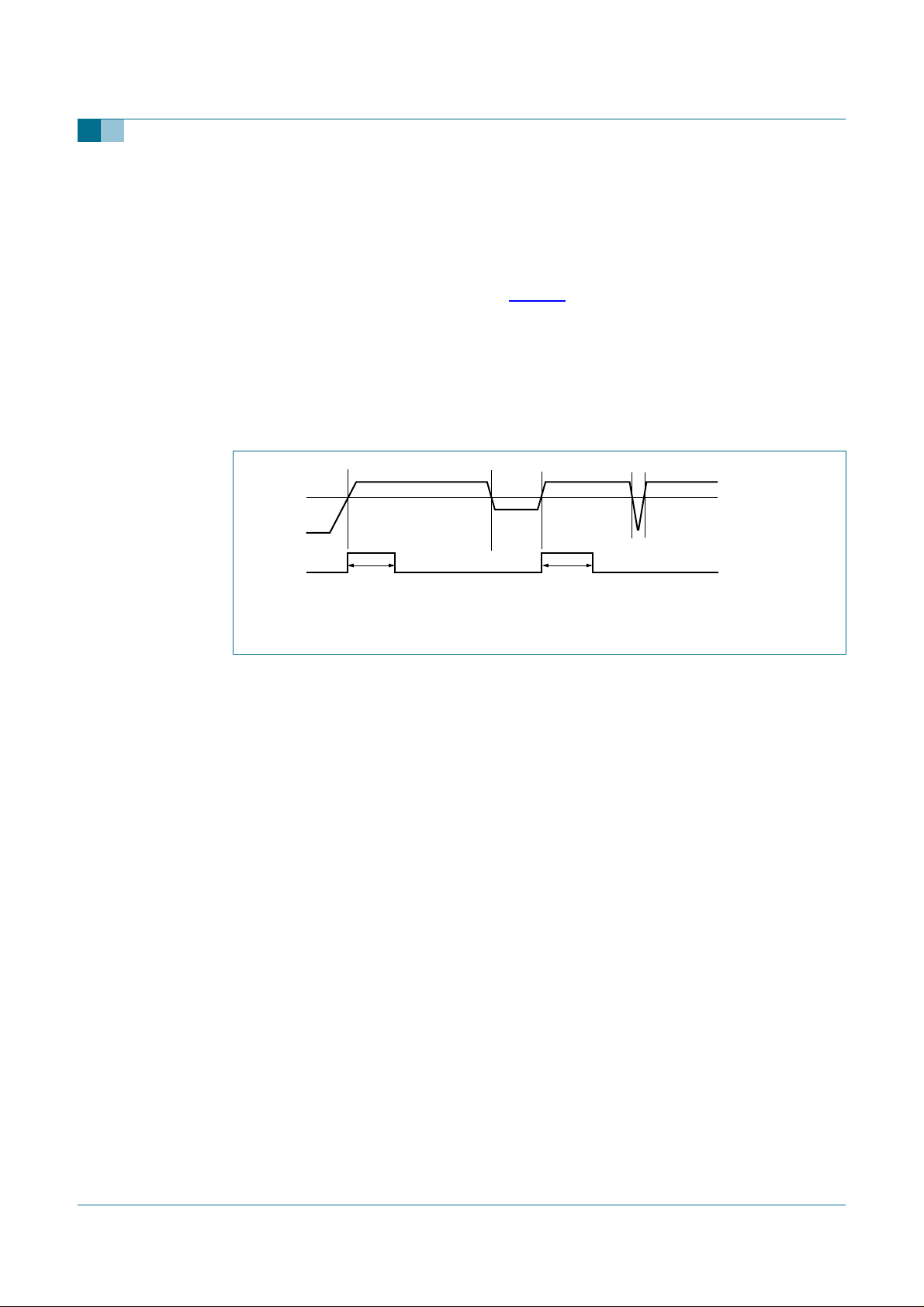
7.10 Power-On Reset (POR)
ISP1109
USB transceiver with carkit support
When V
(t
) will be typically 800 ns. The pulse is started when VCC rises above V
PORP
is directly connected to the RESET_N pin, the internal POR pulse width
CC(I/O)
POR(trip)
(1.5 V to 2.5 V).
To give a better view of the functionality, Figure 6 shows a possible curve of VCCwith dips
at t2 to t3 and t4 to t5. If the dip at t4 to t5 is too short (that is, < 11 µs), the internal POR
pulse will not react and will remain LOW. The internal POR starts with a 1 at t0. At t1, the
detector will see the passing of the trip level and a delay element will add another t
PORP
before it drops to 0.
The internal POR pulse will be generated whenever VCC drops below V
POR(trip)
for more
than 11 µs.
V
CC
V
POR(trip)
t0 t1 t2 t3 t4 t5
(1)
t
PORP
(1) PORP = Power-On Reset Pulse.
Fig 6. Internal power-on reset timing.
t
PORP
004aaa582
PORP
9397 750 13355 © Koninklijke Philips Electronics N.V. 2005. All rights reserved.
Product data sheet Rev. 01 — 14 July 2005 14 of 59
Page 15

Philips Semiconductors
8. Modes of operation
The ISP1109 supports four types of modes:
• Power modes
• Serial control modes
• USB modes
• Transparent modes.
8.1 Power modes
8.1.1 Normal mode
ISP1109
USB transceiver with carkit support
In this mode, both VCC and V
operation range (VCC≥ 3.0 V, V
There are three levels of power saving schemes in the ISP1109:
• Active power mode: Power is on; all circuits are active.
• USB suspend mode: To reduce power consumption, the USB differential receiver is
powered off.
• Power-down mode: Set by writing logic 1 to bit PWR_DN of the Mode Control 2
register. The clock generator and all biasing circuits are turned off to reduce power
consumption to the minimum possible; typically ICC is less than 20 µA. For details on
waking up the clock, see Section 10.
8.1.2 Disable mode
In disable mode, V
Power-down state, if V
When VCC is below threshold V
When V
pin ISET, if any of the following conditions is detected:
BUS>Vth(svc)
• Voltage on pin ID is greater than V
• DP and DM are single-ended one (SE1).
are connected and their voltage levels are within the
CC(I/O)
≥ 1.65 V, V
CC(I/O)
is cut-off and VCC is powered. In this mode, the ISP1109 is in
CC(I/O)
is below SESS_VLD threshold (0.8 V to 2.0 V).
BUS
, pin ISET will remain at the LOW level.
th(ISET)
and VCC rises above V
th(ISET)
th(ID_FM)
≤ VCC).
CC(I/O)
, the ISP1109 will output HIGH on
If the preceding condition is detected, pin ISET will be asserted within 1.5 ms when V
rises above V
The USB differential driver will be set in three-state as long as V
pull-up resistor (R
resistor (R
weakUP(DP)
.
th(ISET)
) will be disconnected from the DP line. The DP weak pull-up
UP(DP)
) will be connected if the V
voltage is above V
BUS
is lost. The DP
CC(I/O)
th(svc)
.
CC
8.1.3 Isolate mode
In isolate mode, VCCis cut-off and V
stable level to all digital output pins, and all bidirectional digital pins will be set in
three-state.
Table 10 shows a summary of power modes.
9397 750 13355 © Koninklijke Philips Electronics N.V. 2005. All rights reserved.
Product data sheet Rev. 01 — 14 July 2005 15 of 59
is powered. In this mode, the ISP1109 will drive
CC(I/O)
Page 16

Philips Semiconductors
ISP1109
USB transceiver with carkit support
Table 10: ISP1109 power modes: summary
V
CC
V
CC(I/O)
V
BUS
PWR_DN (bit) ICC<20µA ISET (pin) Comment
off off X X yes high-Z power off
off on X X yes high-Z isolate mode
on off <V
on off >V
th(svc)
th(svc)
X yes LOW disable mode (Power-down)
X no LOW or HIGH disable mode (ISET operation)
on on X 0 no LOW or HIGH normal mode (full operation)
on on X 1 yes LOW or HIGH normal mode (Power-down)
Table 11 shows the pin states in disable or isolate mode.
Table 11: ISP1109 pin states in disable or isolate mode
Pin name Disable mode
(V
= on, V
CC
, REG3V3 powered not present
V
CC
V
CC(I/O)
, V
REF
not present powered
CC(I/O)
= off)
ISET drive HIGH or LOW high-Z
DP high-Z high-Z
DM 15 kΩ pull-down enabled high-Z
RCV high-Z drive LOW
VP, VM, SPI_MISO, UART_RXD high-Z drive HIGH
RESET_N, SPEED, SUSPEND,
high-Z high-Z
SPI_I2C_SEL, SPI_MOSI/I2C_SDA,
SPI_CLK/I2C_CLK, SPI_CS/I2C_ADR,
SE0/VM, DAT/VP, UART_TXD, INT_N
MIC, SPKR_R, SPKR_L, ID, V
BUS
ID_PU V
high-Z high-Z
(high-Z, if voltage on
REF
pin ID > V
REF
)
Isolate mode
(V
= off, V
CC
(high-Z, if voltage on
V
REF
pin ID > V
REF
CC(I/O)
)
= on)
8.2 Serial control modes
8.2.1 I2C-bus mode
In I2C-bus mode, an external System-on-a-Chip (SoC) directly communicates with the
serial controller through the SCL and SDAlines. The serial controller has a built-in I2C-bus
slave function. An external I2C-bus master can access the internal registers of the
ISP1109 through the I2C-bus interface.
The supported I2C-bus bit rate is up to 400 kbit/s. The I2C-bus device address is
010 110Xb, where X is determined by pin 13.
8.2.2 SPI mode
In this mode, an external SoC directly communicates with the serial controller through the
SPI interface: SPI_MOSI, SPI_MISO, SPI_CLK, SPI_CS. The serial controller has a
built-in SPI slave function. An external SPI master can access the internal registers of the
ISP1109 through the SPI interface. The maximum SPI clock rate is 26 MHz.
9397 750 13355 © Koninklijke Philips Electronics N.V. 2005. All rights reserved.
Product data sheet Rev. 01 — 14 July 2005 16 of 59
Page 17

Philips Semiconductors
8.3 USB modes
The four USB modes of the ISP1109 are:
• VP_VM unidirectional mode
• VP_VM bidirectional mode
• DAT_SE0 unidirectional mode (default)
• DAT_SE0 bidirectional mode.
In VP_VM USB mode, pin DAT/VP is used for the VP function, pin SE0/VM is used for the
VM function, and pin RCV is used for the RCV function.
In DAT_SE0 USB mode, pin DAT/VP is used for the DAT function, pin SE0/VM is used for
the SE0 function, and pin RCV is not used.
In unidirectional mode, pins DAT/VP and SE0/VM are always input. In bidirectional mode,
the direction of these signals depends on input OE_N.
Table 12 specifies the functionality of the device during the four USB modes.
ISP1109
USB transceiver with carkit support
Table 12: USB functional modes: I/O values
USB mode
VP_VM unidirectional 0 0 X TxD+
DAT_SE0 unidirectional 1 0 X TxD
[1] Some of the modes and signals are provided to achieve backward compatibility with IP cores.
[2] TxD+ and TxD− are single-ended inputs to drive the DP and DM outputs, respectively, in single-ended mode.
[3] RxD+ and RxD− are the outputs of the single-ended receivers connected to DP and DM, respectively.
[4] TxD is the input to drive DP and DM in DAT_SE0 mode.
[5] FSE0 is to force an SE0 on the DP and DM lines in DAT_SE0 mode.
[6] RxD is the output of the differential receiver.
[7] RSE0 is an output, indicating that an SE0 is received on the DP and DM lines.
[1]
bidirectional 1 LOW TxD+
bidirectional 1 LOW TxD
Bit Pin
DAT_SE0 BI_DI OE_N DAT/VP SE0/VM VP VM RCV
HIGH RxD+
HIGH RxD
[2]
[2]
[3]
[4]
[4]
[6]
TxD−
TxD−
RxD−
FSE0
FSE0
RSE0
[2]
[2]
[3]
[5]
[5]
[7]
RxD+
[6]
8.4 Transparent modes
8.4.1 Transparent UART mode
RxD−
[6]
RxD
[6]
When in transparent UART mode, an SoC (with the UART controller) communicates
through the ISP1109 to another UART device that is connected to its DP and DM lines.
The ISP1109 operates as logic level translator between the following pins, depending on
the setting of register bit UART_PIN_SEL.
• If UART_PIN_SEL = 0 (default):
– For the TxD signal: From UART_TXD (V
– For the RxD signal: From DP (REG3V3 level) to UART_RXD (REG3V3 level).
9397 750 13355 © Koninklijke Philips Electronics N.V. 2005. All rights reserved.
Product data sheet Rev. 01 — 14 July 2005 17 of 59
level) to DM (REG3V3 level)
CC(I/O)
Page 18

Philips Semiconductors
• If UART_PIN_SEL = 1:
– For the TxD signal: From SE0/VM (V
– For the RxD signal: From DP (REG3V3 level) to DAT/VP (REG3V3 level).
The ISP1109 is in transparent UART mode, if bit UART_ENof the Mode Control 1 register
is set.
8.4.2 Transparent audio mode
In transparent audio mode, the ISP1109 will disable its DP and DM driver. The carkit
interrupt detector is enabled. The built-in analog switches will be tuned based on the
selection of carkit audio mode:
• Stereo mode: SPKR_L on DM and SPKR_R on DP
• Mono and MIC mode: SPKR_L on DM and MIC on DP.
The ISP1109 is in transparent audio mode, if bit UART_EN of the Mode Control 1 register
is cleared, and bit AUDIO_EN of the Audio Control register is set.
8.4.3 Transparent general-purpose buffer mode
USB transceiver with carkit support
level) to DM (REG3V3 level)
CC(I/O)
ISP1109
In transparent general-purpose buffermode, the DAT/VP and SE0/VM pins are connected
to the DP and DM pins, respectively. Using bits TRANSP_BDIR1 and TRANSP_BDIR0 of
the Mode Control 2 register as specified in Table 14, you can control the direction of data
transfer. The ISP1109 is in transparent general-purpose buffer mode if bit UART_EN = 0,
bit AUDIO_EN = 0, and bit TRANSP_EN = 1.
Table 13 provides a summary of the device operating modes.
Table 13: Summary of device operating modes
Mode Bit Description
UART_EN UART_PIN_SEL AUDIO_EN AUDIO_MONO TRANSP_EN
USB mode 0 X 0 X 0 USB ATX enabled
Transparent
general purpose
buffer mode
TransparentAudio
mode (stereo)
TransparentAudio
mode (mono)
TransparentUART
mode (mode 1)
TransparentUART
mode (mode 2)
0 X 0 X 1 USB ATX disabled.
SE0/VM ↔ DM
DAT/VP ↔ DP
Table 14
See
0 X 1 0 X USB ATX disabled.
SPKR_L → DM
SPKR_R → DP
0 X 1 1 X USB ATX disabled.
SPKR_L → DM
MIC ← DP
1 0 X X X USB ATX disabled.
UART_TXD→ DM
UART_RXD← DP
1 1 X X X USB ATX disabled.
SE0/VM → DM
DAT/VP ← DP
9397 750 13355 © Koninklijke Philips Electronics N.V. 2005. All rights reserved.
Product data sheet Rev. 01 — 14 July 2005 18 of 59
Page 19

Philips Semiconductors
Table 14: Transparent general-purpose buffer mode
Bit TRANSP_BDIR[1:0] Direction of the data flow
00 DAT/VP → DP SE0/VM → DM
01 DAT/VP → DP SE0/VM ← DM
10 DAT/VP ← DP SE0/VM → DM
11 DAT/VP ← DP SE0/VM ← DM
ISP1109
USB transceiver with carkit support
9397 750 13355 © Koninklijke Philips Electronics N.V. 2005. All rights reserved.
Product data sheet Rev. 01 — 14 July 2005 19 of 59
Page 20

Philips Semiconductors
USB transceiver with carkit support
9. Serial controller
9.1 Register map
Table 15 provides an overview of the serial controller registers.
Table 15: Register overview
Register Width
(bits)
Vendor ID 16 R 00h to 01h device identification
Product ID 16 R 02h to 03h
Version ID 16 R 14h to 15h
Mode Control 1 8 R/S/C Set — 04h
Mode Control 2 8 R/S/C Set — 12h
Audio Control 8 R/S/C Set — 16h
Timer Control 8 R/S/C Set — 18h
Resistor Control 8 R/S/C Set — 06h
Interrupt Source 8 R Read — 08h interrupt registers
Interrupt Latch 8 R/S/C Set — 0Ah
Interrupt Enable Low 8 R/S/C Set — 0Ch
Interrupt Enable High 8 R/S/C Set — 0Eh
Access Memory
address
Clear — 05h
Clear — 13h
Clear — 17h
Clear — 19h
Clear — 07h
Clear — 0Bh
Clear — 0Dh
Clear — 0Fh
[1]
Functionality Reference
registers
control registers
ISP1109
Section 9.1.1 on page 20
Section 9.1.2 on page 21
Section 9.1.3 on page 24
[1] The R/S/C access type represents a field that can be read, set or cleared (set to 0). A register can be read from either of the indicated
addresses—set or clear. Writing logic 1 to the set address causes the associated bit to be set. Writing logic 1 to the clear address
causes the associated bit to be cleared. Writing logic 0 to an address has no effect.
9.1.1 Device identification registers
9.1.1.1 Vendor ID register
Table 16 provides the bit description of the Vendor ID register.
Table 16: VENDORID - Vendor ID register (address 00h to 01h) bit description
Legend: * reset value
Bit Symbol Access Value Description
15 to 0 VENDORID[15:0] R 04CCh* Philips Semiconductors’ Vendor ID
9.1.1.2 Product ID register
The bit description of the Product ID register is given in Table 17.
9397 750 13355 © Koninklijke Philips Electronics N.V. 2005. All rights reserved.
Product data sheet Rev. 01 — 14 July 2005 20 of 59
Page 21

Philips Semiconductors
ISP1109
USB transceiver with carkit support
Table 17: PRODUCTID - Product ID register (address 02h to 03h) bit description
Legend: * reset value
Bit Symbol Access Value Description
15 to 0 PRODUCTID[15:0] R 1109h* Product ID of the ISP1109
9.1.1.3 Version ID register
Table 18 shows the bit description of the register.
Table 18: VERSIONID - Version ID register (address 14h to 15h) bit description
Legend: * reset value
Bit Symbol Access Value Description
15 to 0 VERSIONID[15:0] R 0110h* Version number of the ISP1109
9.1.2 Control registers
9.1.2.1 Mode Control 1 register
The bit allocation of the Mode Control 1 register is given in Table 19.
Table 19: Mode Control 1 register (address Set = 04h, Clear = 05h) bit allocation
Bit 7 6 5 4 3 2 1 0
Symbol UART_PIN
_SEL
Reset 00000100
Access R/S/C R/S/C R/S/C R/S/C R/S/C R/S/C R/S/C R/S/C
UART_EN reserved TRANSP_ENDAT_SE0 SUSPEND SPEED
Table 20: Mode Control 1 register (address Set = 04h, Clear = 05h) bit description
Bit Symbol Description
7 UART_PIN_
SEL
6 UART_EN When asserted, the ATX is in transparent UART mode.
5 to 4 - reserved; cleared (set to 0)
3 TRANSP_EN When set, the ATX is in transparent mode.
2 DAT_SE0 0 — VP_VM mode
1 SUSPEND Sets the transceiver in low power mode.
0 SPEED Set the rise time and the fall time of the transmit driver in USB modes.
9.1.2.2 Mode Control 2 register
For the bit allocation of this register, see Table 21.
Select UART interface pins for transparent UART mode.
0 — UART_TXD → DM; UART_RXD ← DP
1 — DAT/VP → DP; SE0/VM ← DM.
0 — UART mode is not enabled
1 — UART mode is enabled.
1 — DAT_SE0 mode.
0 — Active power mode
1 — Low power mode (differential receiver is disabled if SPEED = 1).
0 — Low-speed mode
1 — Full-speed mode.
9397 750 13355 © Koninklijke Philips Electronics N.V. 2005. All rights reserved.
Product data sheet Rev. 01 — 14 July 2005 21 of 59
Page 22

Philips Semiconductors
ISP1109
USB transceiver with carkit support
Table 21: Mode Control 2 register (address Set = 12h, Clear = 13h) bit allocation
Bit 7 6 5 4 3 2 1 0
Symbol reserved AUDIO_EN TRANSP_
BDIR1
Reset 0000000 0
Access R/S/C R/S/C R/S/C R/S/C R/S/C R/S/C R/S/C R/S/C
Table 22: Mode Control 2 register (address Set = 12h, Clear = 13h) bit description
Bit Symbol Description
7 to 6 - reserved; cleared (set to 0)
5 AUDIO_EN Enables the ISP1109 in carkit audio mode.
0 — Audio disable: analog switches are turned off, DP_INT detector is
turned off, and single-ended receivers are turned on
1 — Audio enable: analog switches are turned on, DP_INT detector is
turned on, and single-ended receivers are turned off.
4 to 3 TRANSP_
BDIR[1:0]
Controls the direction of data transfer in transparent general-purpose
buffer mode; see
2 BI_DI 0 — Direction of DAT/VP and SE0/VM are fixed (only transmit)
1 — Direction of DAT/VP and SE0/VM are controlled by OE_N.
1 SPD_SUSP_
CTRL
Controls speed and suspend in USB modes:
0 — Controlled by pins SPEED and SUSPEND
1 — Controlled by the Mode Control 1 register bits SPEED and
SUSPEND.
0 PWR_DN Set to Power-down mode; activities on pin SPI_CLK/I2C_SCL or the
interrupt event can wake-up the chip; see
TRANSP_
BDIR0
Table 14
BI_DI SPD_SUSP
_CTRL
Section 9
PWR_DN
9.1.2.3 Audio Control register
Table 23 provides bit allocation of the register.
Table 23: Audio Control register (address Set = 16h, Clear = 17h) bit allocation
Bit 7 6 5 4 3 2 1 0
Symbol PH_ID_
ACK
Reset 00000000
Access R/S/C R/S/C R/S/C R/S/C R/S/C R/S/C R/S/C R/S/C
PH_ID_INT DP_SRP_
EN
ISET_
STATE
ISET_DRV
_EN
SW_MIC_
SPKR_R
SW_MIC_
SPKR_L
Table 24: Audio Control register (address Set = 16h, Clear = 17h) bit description
Bit Symbol Description
7 PH_ID_ACK If set, wait for time t
then turn off. Bit PH_ID_ACK auto-clears to 0. See
6 PH_ID_INT If set, turn on the ID pull-down switch fortime t
Bit PH_ID_INT auto-clears to 0. See
5 DP_SRP_EN Enables the DP pull-up resistor (R
, turn on the ID pull-down switch for t
int(ID)
Wint(ID)
Table 6.
).
UP(DP)
Table 6.
and then turn off.
0 — Disable; DP pull-up can only be enabled using bit DP_PULLUP
when V
is above V
BUS
th(svc)
1 — Enable; DP pull-up is connected.
AUDIO_
MONO
Wint(ID)
,
9397 750 13355 © Koninklijke Philips Electronics N.V. 2005. All rights reserved.
Product data sheet Rev. 01 — 14 July 2005 22 of 59
Page 23

Philips Semiconductors
ISP1109
USB transceiver with carkit support
Table 24: Audio Control register (address Set = 16h, Clear = 17h) bit description
Bit Symbol Description
4 ISET_STATE Determines the logic level for pin ISET when bit ISET_DRV_EN is
logic 1.
0 — ISET outputs LOW
1 — ISET outputs HIGH.
3 ISET_DRV_EN Enables software control of the state of pin ISET:
0 — Disable; the ISET output will be controlled by hardware
1 — Enable; the ISET output will be controlled by bit ISET_STATE.
2 SW_MIC_
SPKR_R
1 SW_MIC_
SPKR_L
0 AUDIO_MONO Selection between stereo and mono audio modes:
Audio loopback test:
0 — Turn off the switch between the MIC and SPKR_R pins
1 — Turn on the switch between the MIC and SPKR_R pins.
Audio loopback test:
0 — Turn off the switch between the MIC and SPKR_L pins
1 — Turn on the switch between the MIC and SPKR_L pins.
0 — Stereo mode: SPKR_L ↔ DM, SPKR_R ↔ DP
1 — Mono mode: SPKR_L ↔ DM, MIC ↔ DP.
9.1.2.4 Timer Control register (S/C: 18h/19h)
The bit allocation of the Timer Control register is given in Table 25.
…continued
Table 25: Timer Control register (address Set = 18h, Clear = 19h) bit allocation
Bit 7 6 5 4 3 2 1 0
Symbol TMR_SE1[3:0] reserved
Reset 00010000
Access R/S/C R/S/C R/S/C R/S/C R/S/C R/S/C R/S/C R/S/C
Table 26: Timer Control register (address Set = 18h, Clear = 19h) bit description
Bit Symbol Description
7 to 4 TMR_SE1[3:0] Program the timer value to detect SE1 on the DP and DM lines. The
interval is 1 ms (Default value = 1 ms).
3 to 0 - reserved
9.1.2.5 Resistor Control register
Table 27 shows the bit allocation of the Resistor Control register.
Table 27: Resistor Control register (address Set = 06h, Clear = 07h) bit allocation
Bit 7 6 5 4 3 2 1 0
Symbol VBUS_
CHRG
Reset 00000011
Access R/S/C R/S/C R/S/C R/S/C R/S/C R/S/C R/S/C R/S/C
VBUS_
DISCHRG
reserved ID_PULLDNDM_PULL
DOWN
DP_PULL
DOWN
DP_WKPU
_EN
DP_PULL
UP
9397 750 13355 © Koninklijke Philips Electronics N.V. 2005. All rights reserved.
Product data sheet Rev. 01 — 14 July 2005 23 of 59
Page 24

Philips Semiconductors
Table 28: Resistor Control register (address Set = 06h, Clear = 07h) bit description
Bit Symbol Description
7 VBUS_CHRG Charge V
6 VBUS_DISCHRG Discharge V
5 reserved reserved; cleared (set to 0)
4 ID_PULLDN Connect pin ID to ground. See
3 DM_PULLDOWN Connect the DM pull-down resistor (R
2 DP_PULLDOWN Connect the DP pull-down resistor (R
1 DP_WKPU_EN Connect the DP weak pull-up resistor (R
0 DP_PULLUP Connect the DP pull-up resistor (R
USB transceiver with carkit support
through a pull-up resistor (R
connected to REG3V3.
BUS
0 — Disconnect the resistor
1 — Connect the resistor.
through a pull-down resistor (R
BUS
0 — Disconnect the resistor
1 — Connect the resistor.
Table 6.
0 — Disconnected
1 — Connected.
0 — DM pull-down resistor is disconnected
1 — DM pull-down resistor is connected.
0 — DP pull-down resistor is disconnected
1 — DP pull-down resistor is connected.
0 — DP weak pull-up resistor is disconnected
1 — DP weak pull-up resistor is connected.
be connected to the DP line only when V
0 — DP pull-up resistor is disconnected
1 — DP pull-up resistor is connected, if V
UP(VBUS)
DN(DM)
).
DN(DP)
weakUP(DP)
). The pull-up resistor will
UP(DP)
BUS>Vth(svc)
BUS>Vth(svc)
ISP1109
) that is
DN(VBUS)
).
).
).
.
.
9.1.3 Interrupt registers
9.1.3.1 Interrupt Source register
Table 29 shows the bit allocation of this register that indicates the current state of the
signals that can generate an interrupt.
Table 29: Interrupt Source register (address 08h) bit allocation
Bit 7 6 5 4 3 2 1 0
Symbol DP_INT reserved ID_FLOAT SE1 ID_GND DP_HI SESS_VLD VBUS_
DET
Reset 00000000
Access RRRRRRRR
9397 750 13355 © Koninklijke Philips Electronics N.V. 2005. All rights reserved.
Product data sheet Rev. 01 — 14 July 2005 24 of 59
Page 25

Philips Semiconductors
Table 30: Interrupt Source register (address 08h) bit description
Bit Symbol Description
7 DP_INT Set to logic 1 when the DP voltage is higher than carkit interrupt
6 - reserved
5 ID_FLOAT Indicates the status of pin ID:
4 SE1 DP and DM SE1 detected. The period of SE1 needed is controlled by
3 ID_GND Indicates the status of pin ID:
2 DP_HI DP single-ended receiver output:
1 SESS_VLD V
0 VBUS_DET V
threshold V
(0.4 V to 0.6 V).
th(DP)L
0 — Voltage on DP is below V
1 — Voltage on DP is above V
0 — ID pin is not floating
1 — ID pin is floating.
TMR_SE1 bits.
0 — SE1 is not detected
1 — SE1 is detected.
0 — ID pin is not grounded
1 — ID pin is grounded.
0 — LOW
1 — HIGH.
session valid detector:
BUS
0 — V
1 — V
BUS
0 — V
1 — V
is lower than V
BUS
is higher than V
BUS
HIGH detector:
is lower than V
BUS
is higher than V
BUS
th(svc)
th(svc)
th(VBUS_HI)
th(VBUS_HI)
ISP1109
USB transceiver with carkit support
th(DP)L
.
th(DP)L
.
.
9.1.3.2 Interrupt Latch register
This register indicates the source that generates an interrupt. For bit allocation, see
Table 31.
Table 31: Interrupt Latch register (address Set = 0Ah, Clear = 0Bh) bit allocation
Bit 7 6 5 4 3 2 1 0
Symbol DP_INT_
INT
Reset 00000000
Access R/S/C R/S/C R/S/C R/S/C R/S/C R/S/C R/S/C R/S/C
9397 750 13355 © Koninklijke Philips Electronics N.V. 2005. All rights reserved.
Product data sheet Rev. 01 — 14 July 2005 25 of 59
reserved ID_FLOAT_
INT
SE1_INT ID_GND_
INT
DP_HI_INT SESS_VLD
_INT
Table 32: Interrupt Latch register (address Set = 0Ah, Clear = 0Bh) bit description
Bit Symbol Description
7 DP_INT_INT 0 — No interrupt
1 — Interrupt on the DP_INT status change.
VBUS_
DET_INT
Page 26

Philips Semiconductors
ISP1109
USB transceiver with carkit support
Table 32: Interrupt Latch register (address Set = 0Ah, Clear = 0Bh) bit description
Bit Symbol Description
6 - reserved
5 ID_FLOAT_INT 0 — No interrupt
1 — Interrupt on the ID_FLOAT status change.
4 SE1_INT 0 — No interrupt
1 — Interrupt on the SE1 status change.
3 ID_GND_INT 0 — No interrupt
1 — Interrupt on the ID_GND status change.
2 DP_HI_INT 0 — No interrupt
1 — Interrupt on the DP_HI status change.
1 SESS_VLD_INT 0 — No interrupt
1 — Interrupt on the SESS_VLD status change.
0 VBUS_DET_INT 0 — No interrupt
1 — Interrupt on the VBUS_DET status change.
9.1.3.3 Interrupt Enable Low register
The bits in this register enable interrupts when the corresponding bits in the Interrupt
Source register changes from logic 1 to logic 0.
Table 33 shows the bit allocation of the register.
…continued
Table 33: Interrupt Enable Low register (address Set = 0Ch, Clear = 0Dh) bit allocation
Bit 7 6 5 4 3 2 1 0
Symbol DP_INT_
IEL
Reset 00000000
Access R/S/C R/S/C R/S/C R/S/C R/S/C R/S/C R/S/C R/S/C
reserved ID_FLOAT_
IEL
Table 34: Interrupt Enable Low register (address Set = 0Ch, Clear = 0Dh) bit description
Bit Symbol Description
7 DP_INT_IEL 0 — Disable
6 - reserved
5 ID_FLOAT_IEL 0 — Disable
4 SE1_IEL 0 — Disable
3 ID_GND_IEL 0 — Disable
2 DP_HI_IEL 0 — Disable
1 SESS_VLD_IEL 0 — Disable
0 VBUS_DET_IEL 0 — Disable
SE1_IEL ID_GND_
IEL
1 — Enable.
1 — Enable.
1 — Enable.
1 — Enable.
1 — Enable.
1 — Enable.
1 — Enable.
DP_HI_IEL SESS_VLD
_IEL
VBUS_
DET_IEL
9397 750 13355 © Koninklijke Philips Electronics N.V. 2005. All rights reserved.
Product data sheet Rev. 01 — 14 July 2005 26 of 59
Page 27

Philips Semiconductors
ISP1109
USB transceiver with carkit support
9.1.3.4 Interrupt Enable High register
The bit allocation of the register is given in Table 35. The bits in this register enable
interrupts when the corresponding bits in the Interrupt Source register changes from
logic 0 to logic 1.
Table 35: Interrupt Enable High register (address Set = 0Eh, Clear = 0Fh) bit allocation
Bit 7 6 5 4 3 2 1 0
Symbol DP_INT_
IEH
Reset 00000000
Access R/S/C R/S/C R/S/C R/S/C R/S/C R/S/C R/S/C R/S/C
reserved ID_FLOAT_
IEH
Table 36: Interrupt Enable High register (address Set = 0Eh, Clear = 0Fh) bit description
Bit Symbol Description
7 DP_INT_IEH 0 — Disable
6 - reserved
5 ID_FLOAT_IEH 0 — Disable
4 SE1_IEH 0 — Disable
3 ID_GND_IEH 0 — Disable
2 DP_HI_IEH 0 — Disable
1 SESS_VLD_IEH 0 — Disable
0 VBUS_DET_IEH 0 — Disable
SE1_IEH ID_GND_
IEH
1 — Enable.
1 — Enable.
1 — Enable.
1 — Enable.
1 — Enable.
1 — Enable.
1 — Enable.
DP_HI_IEH SESS_VLD
_IEH
VBUS_
DET_IEH
9.2 Interrupts
Any of the Interrupt Source register signals given in Table 29 can generate an interrupt
when the signal becomes either LOW or HIGH. After an interrupt is generated, the SoC
can read the status of each signal and the bit that indicates whether or not that signal
generated the interrupt.
A bit in the Interrupt Latch register is set when any of these occurs:
• Writing logic 1 to its set address causes the corresponding bit to be set.
• The corresponding bit in the Interrupt Enable High register is set, and the associated
signal changes from LOW-to-HIGH.
• The corresponding bit in the Interrupt Enable Low register is set, and the associated
signal changes from HIGH-to-LOW.
9397 750 13355 © Koninklijke Philips Electronics N.V. 2005. All rights reserved.
Product data sheet Rev. 01 — 14 July 2005 27 of 59
Page 28

Philips Semiconductors
9.3 SPI interface
9.3.1 Pinout description
The SPI interface consists of four signals as given in Table 37.
Table 37: SPI interface pin description
Pin name Description
SPI_MOSI serial data input line
SPI_MISO serial data output line
SPI_CLK clock input line
SPI_CS clock enable line (active HIGH)
9.3.2 Interface overview
The SPI interface has the following characteristics:
• The maximum clock rate is 26 MHz.
• Data is transmitted, most significant bit first. Each data field consists of a total of
32 bits.
• The data and SPI_CLK signals are ignored, if SPI_CS is LOW. SPI_MISO is set to
three-state, if SPI_CS is programmed LOW.
• SPI_CS is active (HIGH) only during the serial data transmission.
• All input data is sampled at the rising edge of the SPI_CLK signal. Any transition on
SPI_MOSI must occur at least 5 ns before the rising edge of SPI_CLK and remain
stable for at least 5 ns after the rising edge of SPI_CLK.
• All output data is updated at the rising edge of the SPI_CLK signal. Any transition on
SPI_MISO must occur at least 5 ns before the rising edge of SPI_CLK and remain
stable for at least 19.23 ns after the rising edge of SPI_CLK.
• SPI_CS must be active (HIGH) at least 5 ns before the rising edge of the first
SPI_CLK signal, and must remain active (HIGH) at least 61.5 ns after the last falling
edge of SPI_CLK.
• Coincident rising or falling edge of SPI_CLK and SPI_CS are not allowed.
• If SPI_CS goes LOW before enough bits are sent, then the data bits sent are ignored.
• When SPI_CS goes LOW to complete the SPI operation, the next rising edge of
SPI_CS must be delayed by at least 30 ns.
ISP1109
USB transceiver with carkit support
9.3.3 Interface protocol description
The SPI port is configured to use 32-bit serial data words, using 1 bit for R/W, 5 bits for
address, 1 bit for null, and 25 bits for data.
For each SPI transfer,a one is written to pin SPI_MOSI, if this SPI transfer is to be a write.
A zero is written to the pin, if this is to be a read-only command. If a zero is written, then
any data sent after the address bits is ignored and the internal contents of the field
addressed do not change when the 32nd SPI_CLK is sent. Next, the 5-bit address is
written to pin SPI_MOSI MSB first. Finally, data bits are written to the pin MSB first. Once
all the data bits are written, data is transferred to the actual registers on the 32
SPI_CLK. SPI_CS must go LOW and return to HIGH to start the next SPI data transfer.
9397 750 13355 © Koninklijke Philips Electronics N.V. 2005. All rights reserved.
Product data sheet Rev. 01 — 14 July 2005 28 of 59
nd
Page 29

Philips Semiconductors
To read a field of data, pin SPI_MISO will output the data field pointed to by the five
address bits loaded at the beginning of the SPI sequence.
Figure 7 shows the details of an SPI transfer.
SPI_CS
SPI_CLK
ISP1109
USB transceiver with carkit support
SPI_MOSI
SPI_MISO
write_en
Fig 7. SPI transfer.
9.4 I2C-bus protocol
address 4
address 3 address 2 address 1 address 0 dead bit
data 24 data 23
data 24 data 23
Figure 8 shows a multiple read and write by using the SPI bus.
SPI_CS
preamble
SPI_MOSI
SPI_MISO
first address
25-bit data 25-bit data
25-bit data 25-bit data
Fig 8. SPI multiple read and write.
preamble
another address
data 0
data 0
004aaa489
004aaa490
For detailed information, refer to
The I2C-bus Specification; Version 2.1
.
9.4.1 I2C-bus byte transfer format
Table 38: I2C-bus byte transfer format
[1]
S
Byte 1 A
8 bits 8 bits 8 bits ..
[1] S = Start.
[2] A = Acknowledge.
[3] P = Stop.
9397 750 13355 © Koninklijke Philips Electronics N.V. 2005. All rights reserved.
Product data sheet Rev. 01 — 14 July 2005 29 of 59
[2]
Byte 2 A
[2]
Byte 3 A
[2]
.. A
[2]P[3]
Page 30

Philips Semiconductors
ISP1109
USB transceiver with carkit support
9.4.2 I2C-bus device address
Table 39: I2C-bus slave address bit allocation
Bit 7 6 5 4 3 2 1 0
Symbol A6 A5 A4 A3 A2 A1 A0 R/W_N
Value 010110
[1] Determined by logic level on pinI2C_ADR: LOW = 0, HIGH = 1.
Table 40: I2C-bus slave address bit description
Bit Symbol Description
7 to 1 A[6:0] Device address: The device address of the ISP1109 is: 01 0110 (A0).
0 R/W_N Read or write command.
0 — write
1 — read.
[1]
X
9.4.3 Write format
A write operation can be performed as:
• One-byte write to the specified register address
• Multiple-byte write to N consecutive registers, starting from the specified start
address. N defines the number of registers to write to. If N = 1, only the start register
is written.
9.4.3.1 One-byte write
Table 41 describes the transfer format for a one-byte write.
Table 41: Transfer format description for a one-byte write
Byte Description
S master starts with a START condition
Device select master transmits device address and write command bit R/W = 0
ACK slave generates an acknowledgment
Register address K master transmits address of register K
ACK slave generates an acknowledgment
Write data K master writes data to register K
ACK slave generates an acknowledgment
P master generates a STOP condition
9.4.3.2 Multiple-byte write
Table 42 describes the transfer format for a multiple-byte write.
Table 42: Transfer format description for a multiple-byte write
Byte Description
S master starts with a START condition
Device select master transmits device address and write command bit R/W = 0
ACK slave generates an acknowledgment
9397 750 13355 © Koninklijke Philips Electronics N.V. 2005. All rights reserved.
Product data sheet Rev. 01 — 14 July 2005 30 of 59
Page 31

Philips Semiconductors
ISP1109
USB transceiver with carkit support
Table 42: Transfer format description for a multiple-byte write
…continued
Byte Description
Register address K master transmits address of register K. This is the start address for
writing multiple data bytes to consecutive registers. After a byte is written,
the register address is automatically incremented by 1.
Remark: If the master writes to a nonexistent register, the slave must
send a 'not ACK' and also must not increment the index address.
ACK slave generates an acknowledgment
Write data K master writes data to register K
ACK slave generates an acknowledgment
Write data K + 1 master writes data to register K + 1
ACK slave generates an acknowledgment
::
Write data K + N − 1 master writes data to register K + N − 1. When the incremented address
K+N− 1 becomes > 255, the register address rolls over to 0. Therefore,
it is possible that some registers may be overwritten, if the transfer is not
stopped before the rollover.
ACK slave generates an acknowledgment
P master generates a STOP condition
Figure 9 illustrates the write format for a one-byte write and a multiple-byte write.
S
device select
S
device select
write data K + 2
Fig 9. Writing data to the ISP1109 registers.
9.4.4 Read format
A read operation can be performed in two ways:
• Current address read: to read the register at the current address.
– Single-register read.
• Random address read: to read N registers starting at a specified address. N defines
the number of registers to be read. If N = 1, only the start register is read.
– Single-register read
ACK
wr
wr
register address K
one-byte write
ACK
register address K
ACK
write data K + 3
multiple-byte write
ACK
write data K
ACK
write data K
ACK
.... maximum, rollover to 0
ACK
P
ACK
write data K + 1
ACK
write data K + N - 1
ACK
ACK
P
004aaa569
9397 750 13355 © Koninklijke Philips Electronics N.V. 2005. All rights reserved.
Product data sheet Rev. 01 — 14 July 2005 31 of 59
Page 32

Philips Semiconductors
– Multiple-register read.
9.4.4.1 Current address read
The transfer format description for a current address read is given in Table 43. For
illustration, see Figure 10.
Table 43: Transfer format description for current address read
Byte Description
S master starts with a START condition
Device select master transmits device address and read command bit R/W = 1
ACK slave generates an acknowledgment
Read data K slave transmits and master reads data from register K. If the start address is
No ACK master terminates the read operation by generating a No Acknowledge
P master generates a stop condition
ISP1109
USB transceiver with carkit support
not specified, the read operation starts from where the index register is
pointing to because of a previous read or write operation.
S
device select
Fig 10. Current address read.
9.4.4.2 Random address read—Single read
Table 44 describes the transfer format for a single-byte read. Figure 11 illustrates the byte
sequence.
Table 44: Transfer format description for single-byte read
SDA line Description
S master starts with a START condition
Device select master transmits device address and write command bit R/W = 0
ACK slave generates an acknowledgment
Register address K master transmits (start) address of register K to be read from
ACK slave generates an acknowledgment
S master restarts with a START condition
Device select master transmits device address and read command bit R/W = 1
ACK slave generates an acknowledgment
Read data K slave transmits and master reads data from register K
No ACK master terminates the read operation by generating a No Acknowledge
P master generates a STOP condition
ACK
rd
current address read
read data K
no ACK
P
004aaa570
9.4.4.3 Random address read—Multiple read
The transfer format description for a multiple-byte read is given in Table 45. Figure 11
illustrates the byte sequence.
9397 750 13355 © Koninklijke Philips Electronics N.V. 2005. All rights reserved.
Product data sheet Rev. 01 — 14 July 2005 32 of 59
Page 33

Philips Semiconductors
Table 45: Transfer format description for a multiple-byte read
SDA line Description
S master starts with a START condition
Device select master transmits device address and write command bit R/W = 0
ACK slave generates an acknowledgment
Register address K master transmits (start) address of register K to be read from
ACK slave generates an acknowledgment
S master restarts with a START condition
Device select master transmits device address and read command bit R/W = 1
ACK slave generates an acknowledgment
Read data K slave transmits and master reads data from register K. After a byte is read,
ACK slave generates an acknowledgment
Read data K + 1 slave transmits and master reads data from register K + 1
ACK slave generates an acknowledgment
::
Read data K + N − 1 slave transmits and master reads data register K + N − 1. This is the last
No ACK master terminates the read operation by generating a No Acknowledge
P master generates a STOP condition
ISP1109
USB transceiver with carkit support
the address is automatically incremented by 1.
register to read. After incrementing, the address rolls over to 0. Here, N
represents the number of addresses available in the slave.
ACK
S
device select
device select
S
read data K + 1
wr
ACK
wr
ACK
register address K
register address K
read data K + 2
Fig 11. Random address read.
10. Clock wake-up scheme
This section explains the ISP1109 clock stop timing, events triggering the clock to wake
up, and the timing of the clock wake-up.
ACK
S
device select
random address single read
ACK
S
device select
ACK
.... maximum, rollover to 0
random access multiple read
ACK
rd
ACK
rd
ACK
write data K + N - 1
read data K
read data K
no ACK
P
ACK
no ACK
P
004aaa571
9397 750 13355 © Koninklijke Philips Electronics N.V. 2005. All rights reserved.
Product data sheet Rev. 01 — 14 July 2005 33 of 59
Page 34

Philips Semiconductors
10.1 Power-down event
ISP1109
USB transceiver with carkit support
If V
(0.8 V to 2.0 V), the ISP1109 is in Power-down mode and internal clocks are turned off.
The internal clock—LazyClock or I2C-bus clock or both—is stopped when bit PWR_DN is
set. It takes approximately 8 ms for the clock to stop from the time the Power-down
condition is detected.
If SPI mode is selected, a register read or write access is normal, as when in Power-down
mode. If I2C-bus mode is selected, the internal clock must first be woken up before any
register read or write operation.
is not present and the V
CC(I/O)
10.2 Clock wake-up event
The clock wakes up when any of the following events occurs on ISP1109 pins:
• Pin SPI_CLK/I2C_SCL goes LOW, if I
HIGH).
• Pin V
bit SESS_VLD_IEH of the Interrupt Enable High register is set.
goes above the session valid threshold (0.8 V to 2.0 V), provided
BUS
• Status bit ID_FLOAT changes from logic 1 to logic 0, provided bit ID_FLOAT_IEL of
the Interrupt Enable Low register is set.
• Status bit ID_FLOAT changes from logic 0 to logic 1, provided bit ID_FLOAT_IEH of
the Interrupt Enable High register is set.
• Status bit SE1 changes from logic 0 to logic 1, provided bit SE1_IEH of the Interrupt
Enable High register is set.
voltage is below the SESS_VLD threshold
BUS
2
C-bus mode is selected (pin SPI_I2C_SEL is
The event triggers the clock to start. A stable clock is guaranteed within 100 µs.
When an event is triggered and the clock is started, it will remain active for approximately
8 ms. If bit PWR_DN is not cleared within this 8 ms period, the clock will stop. If the clock
wakes up because of any event other than SPI_CLK/I2C_SCL going LOW, an interrupt
will be generated once the clock is active.
11. Electro-Static Discharge (ESD)
11.1 ESD protection
The pins that are connected to the USB connector—DP, DM, ID, V
GNDD—have a minimum of ±12 kV ESD protection. The ±12 kV measurement is limited
by the test equipment. Capacitors of 4.7 µF connected from REG3V3 to GNDA and V
to GNDA are required to achieve this ±12 kV ESD protection. See Figure 12.
, VCC, GNDA and
BUS
BUS
9397 750 13355 © Koninklijke Philips Electronics N.V. 2005. All rights reserved.
Product data sheet Rev. 01 — 14 July 2005 34 of 59
Page 35

Philips Semiconductors
ISP1109
USB transceiver with carkit support
charge current
limit resistor
HIGH VOLTAGE
DC SOURCE
Fig 12. Human Body ESD test model.
11.2 ESD test conditions
A detailed report on test setup and results is available on request.
R
1 MΩ
C
100 pF
R
D
1500 Ω
discharge
resistance
A
C
S
storage
capacitor
B
DEVICE UNDER
TEST
4.7 µF
V
BUS
REG3V3
4.7 µF
GND
004aaa580
9397 750 13355 © Koninklijke Philips Electronics N.V. 2005. All rights reserved.
Product data sheet Rev. 01 — 14 July 2005 35 of 59
Page 36

Philips Semiconductors
ISP1109
USB transceiver with carkit support
12. Limiting values
Table 46: Limiting values
In accordance with the Absolute Maximum Rating System (IEC 60134).
Symbol Parameter Conditions Min Max Unit
Voltage
V
CC
V
CC(I/O)
V
I
V
BUS
V
I(ID)
V
esd
Current
I
lu
supply voltage −0.5 +7.0 V
I/O supply voltage −0.5 +4.6 V
input voltage
V
input voltage −0.5 +7.0 V
BUS
[1]
−0.5 V
CC(I/O)
+ 0.5 V V
ID input voltage −0.5 +5.5 V
electrostatic discharge voltage ILI<1µA
pins DP, DM, ID, V
V
, GNDA and GNDD
CC
BUS
,
−12 +12 kV
[2] [3]
all other pins −2+2 kV
latch-up current - 100 mA
[1] Input voltage on all digital pins.
[2] Testing equipment limits measurement to only ±12 kV. 4.7 µF capacitors needed on V
[3] Equivalent to discharging a 100 pF capacitor through a 1.5 kΩ resistor (Human Body Model).
and REG3V3 (see Section 11).
BUS
13. Recommended operating conditions
Table 47: Recommended operating conditions
Symbol Parameter Conditions Min Typ Max Unit
Voltage
V
CC
V
CC(I/O)
V
REF
V
I
V
I(AI/O)
V
O(OD)
Temperature
T
amb
[1] V
CC(I/O)
[2] Input voltage on all digital pins.
supply voltage 3.0 - 5.25 V
I/O supply voltage
[1]
1.65 - 3.6 V
audio supply voltage 2.65 - 3.0 V
input voltage
input voltage on analog I/O
[2]
0- V
CC(I/O)
0 - 3.6 V
pins DP and DM
open-drain output pull-up voltage 1.65 - 3.6 V
ambient temperature −40 - +85 °C
must be less than or equal to VCC.
V
9397 750 13355 © Koninklijke Philips Electronics N.V. 2005. All rights reserved.
Product data sheet Rev. 01 — 14 July 2005 36 of 59
Page 37

Philips Semiconductors
ISP1109
USB transceiver with carkit support
14. Static characteristics
Table 48: Static characteristics: supply pins
VCC= 3.0 V to 5.25 V; V
Symbol Parameter Conditions Min Typ Max Unit
Voltage
V
O(REG3V3)
regulated supply voltage
output
Current
I
CC
I
CC(I/O)
I
CC(I/O)(isolate)
I
CC(idle)
operating supply current transmitting and receiving at
operating I/O supply current transmitting and receiving at
isolate mode I/O supply current VCC not connected - - 10 µA
supply current during
full-speed idle and SE0
I
CC(I/O)(static)
I
CC(pd)
static I/O supply current idle, SE0 or suspend - - 20 µA
Power-down mode supply
current
I
VREF
supply current on pin V
= 1.65 V to 3.6 V; T
CC(I/O)
REF
=−40°Cto+85°C; unless otherwise specified.
amb
I
≤ 300 µA
LOAD
12 Mbit/s; C
= 50 pF on
L
[1]
3.0 3.3 3.6 V
[2]
- 48mA
pins DP and DM
[2]
- 12mA
12 Mbit/s
idle: VDP> 2.7 V, VDM< 0.3 V;
SE0: V
< 0.3 V, VDM< 0.3 V
DP
bit PWR_DN = 1 or
V
CC(I/O)
=0V
[3]
- - 300 µA
[3]
--20µA
- - 100 µA
[1] In Power-down mode, the minimum voltage is 2.7 V.
[2] Maximum value characterized only, not tested in production. Typical value measured at VCC=5V, V
[3] Excluding any load current to the 1.5 kΩ and 15 kΩ pull-up and pull-down resistors (200 µA typical).
CC(I/O)
= 1.8 V and T
amb
=25°C.
Table 49: Static characteristics: digital pins (except for ISET)
VCC= 3.0 V to 5.25 V; V
= 1.65 V to 3.6 V; T
CC(I/O)
=−40°Cto+85°C; unless otherwise specified.
amb
Symbol Parameter Conditions Min Typ Max Unit
Input level voltage
V
IL
V
IH
LOW-level input voltage - - 0.3V
HIGH-level input voltage 0.6V
CC(I/O)
-- V
CC(I/O)
V
Output level voltage
V
OL
V
OH
LOW-level output voltage IOL= 2 mA - - 0.4 V
= 100 µA - - 0.15 V
I
OL
HIGH-level output voltage IOH=2mA
= 100 µAV
I
OH
[1]
V
− 0.4 V - - V
CC(I/O)
− 0.15 V - - V
CC(I/O)
Leakage current
I
LI
input leakage current
[2]
−1-+1µA
Open-drain output current
I
OZ
OFF-state output current −5-+5µA
Capacitance
C
IN
input capacitance pin to GND - - 10 pF
[1] Not applicable for open-drain outputs.
[2] V
9397 750 13355 © Koninklijke Philips Electronics N.V. 2005. All rights reserved.
Product data sheet Rev. 01 — 14 July 2005 37 of 59
is not greater than V
CC(I/O)
O(REG3V3)
.
Page 38

Philips Semiconductors
ISP1109
USB transceiver with carkit support
Table 50: Static characteristics: digital pin ISET
VCC= 3.0 V to 5.25 V; V
Symbol Parameter Conditions Min Typ Max Unit
Voltage
V
th(ISET)
VCC threshold voltage for ISET
function
V
OH(ISET)
VOH on pin ISET VCC≥ 3.0 V 2.4 - - V
Timing
t
d(ISET)
time from ISET condition to the
ISET pin HIGH
Table 51: Static characteristics: analog I/O pins DP and DM
VCC= 3.0 V to 5.25 V; V
Symbol Parameter Conditions Min Typ Max Unit
Input level voltage
V
DI
V
CM
differential input sensitivity |VDP− VDM| 0.2 - - V
differential common mode
voltage
V
IL
V
IH
LOW-level input voltage - - 0.8 V
HIGH-level input voltage 2.0 - - V
Output level voltage
V
OL
V
OH
LOW-level output voltage RLof 1.5 kΩ to +3.6 V - - 0.3 V
HIGH-level output voltage RLof 15 kΩ to GND 2.8 - 3.6 V
Voltage
V
th(DP)L
V
TERM
DP LOW threshold 0.4 - 0.6 V
termination voltage for the
upstream port pull-up resistor
(R
)
PU
Leakage current
I
LZ
OFF-state leakage current −1- +1µA
Capacitance
C
IN
input capacitance pin to GNDA - - 10 pF
Resistance
R
PD
pull-down resistance on pins DP
and DM
R
UP(DP)
R
weakUP(DP)
pull-up resistance on pin DP bus idle 900 - 1575 Ω
weak pull-up resistance on
pin DP
Z
DRV
Z
INP
driver output impedance steady-state drive
input impedance 10 - - MΩ
= 1.65 V to 3.6 V; T
CC(I/O)
= 1.65 V to 3.6 V; T
CC(I/O)
=−40°Cto+85°C; unless otherwise specified.
amb
1.5 - 2.5 V
< 3.0 V 0.8V
V
CC
CC
--V
- - 1.5 ms
=−40°Cto+85°C; unless otherwise specified.
amb
includes VDI range 0.8 - 2.5 V
3.0 - 3.6 V
14.25 - 24.8 kΩ
bus driven 1425 - 3090 Ω
91 - 169 kΩ
[1]
34 - 44 Ω
[1] Includes external series resistors of 33 Ω±1 % each on DP and DM.
9397 750 13355 © Koninklijke Philips Electronics N.V. 2005. All rights reserved.
Product data sheet Rev. 01 — 14 July 2005 38 of 59
Page 39

Philips Semiconductors
ISP1109
USB transceiver with carkit support
Table 52: Static characteristics: analog I/O pins ID and ID_PU
VCC= 3.0 V to 5.25 V; V
Symbol Parameter Conditions Min Typ Max Unit
Voltage
V
th(ID_GND)
V
th(ID_FLOAT)
V
th(ID_FM)
ID_GND comparator threshold 0.2 - 0.8 V
ID_FLOAT comparator threshold 2.0 - V
ID factory mode detector
threshold
Resistance
R
PU_ID
ID pull-up switch impedance
between pins ID_PU and V
R
PD_ID
ID impedance to GND bit ID_PULLDOWN = 1 - - 50 Ω
= 1.65 V to 3.6 V; T
CC(I/O)
REF
=−40°Cto+85°C; unless otherwise specified.
amb
3.0 - 3.8 V
- - 500 Ω
O(REG3V3)
− 0.2 V V
Table 53: Static characteristics: analog I/O pin V
VCC= 3.0 V to 5.25 V; V
= 1.65 V to 3.6 V; T
CC(I/O)
BUS
=−40°Cto+85°C; unless otherwise specified.
amb
Symbol Parameter Conditions Min Typ Max Unit
Voltage
V
V
th(VBUS_HI)
V
th(svc)
detector 3.0 - 3.8 V
BUS
V
session valid comparator
BUS
0.8 - 2.0 V
threshold
V
hys(svc)
session valid comparator
BUS
- 200 - mV
V
hysteresis
Resistance
R
UP(VBUS)
pull-up resistance on pin V
connect to REG3V3
BUS
460 - 1000 Ω
when VBUS_CHRG = 1
R
DN(VBUS)
pull-down resistance on
pin V
BUS
connect to GND when
VBUS_DISCHRG = 1
660 - 1200 Ω
Table 54: Static characteristics: analog I/O pins SPKR_L, SPKR_R and MIC
VCC= 3.0 V to 5.25 V; V
= 1.65 V to 3.6 V; T
CC(I/O)
=−40°Cto+85°C; unless otherwise specified.
amb
Symbol Parameter Conditions Min Typ Max Unit
Capacitance
C
IN
input capacitance pin to GNDA - - 10 pF
Impedance
Z
asw(on)
Z
asw(off)
audio switch ON state impedance 0 kHz to 20 kHz 50 - 150 Ω
audio switch OFF state impedance 0 kHz to 20 kHz 2 - - MΩ
9397 750 13355 © Koninklijke Philips Electronics N.V. 2005. All rights reserved.
Product data sheet Rev. 01 — 14 July 2005 39 of 59
Page 40

Philips Semiconductors
ISP1109
USB transceiver with carkit support
15. Dynamic characteristics
Table 55: Dynamic characteristics: reset and clock
VCC= 3.0 V to 5.25 V; V
Symbol Parameter Conditions Min Typ Max Unit
Reset
t
W(RESET_N)
pulse width on input RESET_N 10 - - µs
Internal clock
f
clk
clock frequency bit GLOBAL_PWR_DN = 0 70 100 130 kHz
Table 56: Dynamic characteristics: bus turnaround timing (USB bidirectional mode)
VCC= 3.0 V to 5.25 V; V
otherwise specified.
Symbol Parameter Conditions Min Typ Max Unit
t
TOI
bus turnaround time
(OE_N to DAT/VP and SE0/VM)
t
TIO
bus turnaround time
(OE_N to DAT/VP and SE0/VM)
= 1.65 V to 3.6 V; T
CC(I/O)
= 1.65 V to 3.6 V; CL= 50 pF; RPU= 1.5 kΩon DP to V
CC(I/O)
=−40°Cto+85°C; unless otherwise specified.
amb
output-to-input;
see
Figure 17
input-to-output;
see
Figure 17
TERM;Tamb
=−40°Cto+85°C; unless
0- 5ns
0- 5ns
Table 57: Dynamic characteristics: analog I/O pins DP and DM
VCC= 3.0 V to 5.25 V; V
= 1.65 V to 3.6 V; CL= 50 pF; RPU= 1.5 kΩon DP to V
CC(I/O)
TERM;Tamb
=−40°Cto+85°C; unless
otherwise specified.
Symbol Parameter Conditions Min Typ Max Unit
Driver characteristics
t
FR
t
FF
rise time CL= 50 pF to 125 pF;
fall time CL= 50 pF to 125 pF;
FRFM differential rise time and fall time
FR/tFF
)
V
CRS
matching (t
output signal crossover voltage excluding the first transition
10%to90%of|V
see
Figure 13
90%to10%of|V
see
Figure 13
OH
OH
− VOL|;
− VOL|;
excluding the first transition
from the idle state
4 - 20 ns
4 - 20 ns
90 - 111.1 %
[1]
1.3 - 2.0 V
from the idle state;
see
Figure 14
Driver timing
t
PLH(drv)
t
PHL(drv)
t
PHZ
t
PLZ
t
PZH
t
PZL
propagation delay
(DAT/VP, SE0/VM to DP, DM)
propagation delay
(DAT/VP, SE0/VM to DP, DM)
disable delay
(OE_N to DP, DM)
disable delay
(OE_N to DP, DM)
enable delay
(OE_N to DP, DM)
enable delay
(OE_N to DP, DM)
LOW-to-HIGH;
see
Figure 14 and Figure 21
HIGH-to-LOW;
see
Figure 14 and Figure 21
HIGH-to-OFF;
see
Figure 15 and Figure 22
LOW-to-OFF;
see
Figure 15 and Figure 22
OFF-to-HIGH;
see
Figure 15 and Figure 22
OFF-to-LOW;
see
Figure 15 and Figure 22
- - 18 ns
- - 18 ns
- - 15 ns
- - 15 ns
- - 15 ns
- - 15 ns
9397 750 13355 © Koninklijke Philips Electronics N.V. 2005. All rights reserved.
Product data sheet Rev. 01 — 14 July 2005 40 of 59
Page 41

Philips Semiconductors
ISP1109
USB transceiver with carkit support
Table 57: Dynamic characteristics: analog I/O pins DP and DM
VCC= 3.0 V to 5.25 V; V
= 1.65 V to 3.6 V; CL= 50 pF; RPU= 1.5 kΩon DP to V
CC(I/O)
…continued
TERM;Tamb
=−40°Cto+85°C; unless
otherwise specified.
Symbol Parameter Conditions Min Typ Max Unit
Receiver timing
Differential receiver
t
PLH(rcv)
t
PHL(rcv)
propagation delay
(DP, DM to RCV)
propagation delay
(DP, DM to RCV)
LOW-to-HIGH;
see
Figure 16 and Figure 23
HIGH-to-LOW;
see
Figure 16 and Figure 23
- - 15 ns
- - 15 ns
Single-ended receiver
t
PLH(se)
propagation delay (DP, DM to VP
and DAT/VP, VM and SE0/VM)
t
PHL(se)
propagation delay (DP, DM to VP
and DAT/VP, VM and SE0/VM)
[1] Characterized only; not tested. Limits guaranteed by design.
LOW-to-HIGH;
see
Figure 16 and Figure 23
HIGH-to-LOW;
see
Figure 16 and Figure 23
- - 18 ns
- - 18 ns
Table 58: Dynamic characteristics: analog I/O pin ID
VCC= 3.0 V to 5.25 V; V
= 1.65 V to 3.6 V; CL= 50 pF; RPU= 1.5 kΩon DP to V
CC(I/O)
TERM;Tamb
=−40°Cto+85°C; unless
otherwise specified.
Symbol Parameter Conditions Min Typ Max Unit
t
Wint(ID)
t
int(ID)
ID interrupt pulse width 4 - 8 ms
ID interrupt wait time 4 - 8 ms
Table 59: Dynamic characteristics: audio switches
VCC= 3.0 V to 5.25 V; V
= 1.65 V to 3.6 V; CL= 50 pF; RPU= 1.5 kΩon DP to V
CC(I/O)
TERM;Tamb
=−40°Cto+85°C; unless
otherwise specified.
Symbol Parameter Conditions Min Typ Max Unit
PSRR Power Supply Rejection Ratio;
Section 17.1
see
: V
noise on V
CC
(p-p)
= 0.5 V,
f = 217 Hz, 20 Hz to 20 kHz
noiseonV
REF:V(p-p)
=50mV,
[1]
--−80 dB
[1]
--−45 dB
f=20Hzto20kHz
α
ct(audio)
crosstalk audio;
see
Section 17.2
THD Total Harmonic Distortion;
see
Section 17.1
α
iso(d-a)
data to audio isolation;
see
Section 17.3
=1V, f=1kHz
V
(p-p)
= 2.3 V, f = 1 kHz
V
(p-p)
= 2.0 V, f = 1 kHz
V
(p-p)
USB 12 Mbit active on DP
and DM, < 20 kHz signal
[1]
--−66 dB
[1]
--1%
[1]
- - 0.3 %
--−70 dB
components observed on the
SPKR_L, SPKR_R or MIC
pins
V
io(aud)
audio input or output voltage
0.1 - 2.55 V
range
[1] V
indicates peak-to-peak voltage, and f indicates frequency.
(p-p)
9397 750 13355 © Koninklijke Philips Electronics N.V. 2005. All rights reserved.
Product data sheet Rev. 01 — 14 July 2005 41 of 59
Page 42

Philips Semiconductors
ISP1109
USB transceiver with carkit support
1.8 V
logic input
tFR, t
V
OH
V
OL
LR
90 %
10 %
90 %
tFF, t
10 %
LF
004aaa572
V
0 V
V
OH
OL
0.9 V
differential
data lines
t
PLH(drv)
V
CRS
Fig 13. Rise and fall times. Fig 14. Timing of DAT/VP and SE0/VM to DP and DM.
0.9 V
t
PHL(drv)
V
CRS
004aaa573
1.8 V
0 V
V
OH
V
OL
logic
0.9 V
input
differential
data lines
t
PZH
t
PZL
V
CRS
0.9 V
t
PHZ
t
PLZ
V
−0.3 V
OH
+0.3 V
V
OL
004aaa574
2.0 V
differential
data lines
0.8 V
V
OH
logic output
V
OL
V
CRS
t
PLH(rcv)
t
PLH(se)
0.9 V
V
CRS
t
PHL(rcv)
t
PHL(se)
0.9 V
004aaa575
Fig 15. Timing of OE_N to DP and DM. Fig 16. Timing of DP and DM to RCV, VP or DAT/VPand
VM or SE0/VM.
OE_N
t
TIO
004aaa521
DAT/VP
SE0/VM
t
TOI
output input output
Fig 17. SIE interface bus turnaround timing.
9397 750 13355 © Koninklijke Philips Electronics N.V. 2005. All rights reserved.
Product data sheet Rev. 01 — 14 July 2005 42 of 59
Page 43

Philips Semiconductors
15.1 SPI bus characteristics
ISP1109
USB transceiver with carkit support
t
t
h(SPI_CS)
(SPI_CS)LH
t
r(SPI_CS)
t
W(SPI_CLK)
SPI_CS
SPI_CLK
SPI_MOSI
SPI_MISO
t
su(SPI_MOSI)
T
SPI_CLK
t
h(SPI_MOSI)
t
W(SPI_CLK)
dead
bit
CLK
t
su(SPI_MISO)
t
h(SPI_MISO)
004aaa488
Fig 18. SPI timing diagram.
Table 60: SPI timing
Symbol Parameter Min Max Unit
T
SPI_CLK
t
W(SPI_CLK)
t
rf(SPI_CLK)
t
(SPI_CS)LH
t
r(SPI_CS)
t
h(SPI_CS)
t
su(SPI_MOSI)
t
h(SPI_MOSI)
t
su(SPI_MISO)
t
h(SPI_MISO)
SPI_CLK cycle time 38.46 - ns
SPI_CLK HIGH or LOW time 19.23 - ns
SPI_CLK rise or fall time 7.6 - ns
transfer delay time between queues (SPI_CS from falling edge to rising edge) 30 - ns
SPI_CS rise time (SPI_CS setup to SPI_CLK first rise edge) 10 - ns
SP_CS hold time (SPI_CS hold after SPI_CLK last fall edge) 61.5 - ns
SPI_MOSI setup time (SPI_MOSI valid to SPI_CLK rise edge) 5 - ns
SPI_MOSI hold time (SPI_CLK rise edge to SPI_MOSI valid) 5 - ns
SPI_MISO setup time (SPI_MISO valid to SPI_CLK rise edge) 5 - ns
SPI_MISO hold time (SPI_CLK rise edge to SPI_MISO valid) 19.23 - ns
2
C-bus characteristics
t
r
t
(SCL)L
t
HD;STA
S
t
HD;DAT
t
SU;DAT
t
(SCL)H
t
f
t
SU;STA
t
HD;STA
Sr
t
SP
t
SU;STO
t
t
r
BUF
P
S
004aaa577
SDA
SCL
15.2 I
t
f
Fig 19. Definition of timing for standard-mode or fast-mode devices on the I2C-bus.
9397 750 13355 © Koninklijke Philips Electronics N.V. 2005. All rights reserved.
Product data sheet Rev. 01 — 14 July 2005 43 of 59
Page 44

Philips Semiconductors
ISP1109
USB transceiver with carkit support
Table 61: Characteristics of I/O stages of I2C-bus lines (SDA, SCL)
Symbol Parameter Conditions Standard mode Fast mode Unit
Min Max Min Max
f
SCL
t
HD;STA
t
(SCL)L
t
(SCL)H
t
SU;STA
t
SU;DAT
t
HD:DAT
t
r
t
f
t
SU;STO
t
BUF
SCL clock frequency 0 100 0 400 kHz
hold time for the START
4.0 - 0.6 - µs
condition
LOW period of the SCL clock 4.7 - 1.3 - µs
HIGH period of the SCL clock 4.0 - 0.6 - µs
setup time for the START
4.7 - 0.6 - µs
condition
data setup time 250 - 100 - ns
data hold time 0 - 0 0.9 µs
rise time SDA and SCL signals - 1000 20 + 0.1 C
fall time SDA and SCL signals - 300 20 + 0.1 C
setup time for the STOP
4.0 - 0.6 - µs
[1]
b
[1]
b
300 ns
300 ns
condition
bus free time between a
4.7 - 1.3 - µs
STOP and START condition
[1] Cb is the capacitive load for each bus line in pF. If mixed with high-speed mode devices, faster fall times are allowed.
9397 750 13355 © Koninklijke Philips Electronics N.V. 2005. All rights reserved.
Product data sheet Rev. 01 — 14 July 2005 44 of 59
Page 45

Philips Semiconductors
16. Application information
V
(1.65 V to 3.6 V)
CC(I/O)
10 kΩ ± 5 %
PHONE
PROCESSOR
SPI
UART
USB
0.01 µF
SPI_CLK/I2C_SCL
SPI_MOSI/I2C_SDA
V
10 kΩ ± 5 %
0.1 µF
SYS_RST
RESET_N
INT_N
SPI_I2C_SEL
SPI_CS/I2C_ADR
SPI_MISO
UART_TXD
UART_RXD
OE_N
DAT/VP
SE0/VM
RCV
VP
VM
CC(I/O)
SPEED
10 kΩ ± 5 %
SUSPEND
8
5
4
9
13
12
11
10
25
26
20
18
17
16
15
14
6
7
V
CC(I/O)
V
CC(I/O)
19 3
ISP1109
GNDD
(exposed
die pad)
V
REF
CC
31
V
0.1 µF
REF
21
24
GNDA
(2.65 V to 3.0 V)
V
0.1 µF
0.1 µF
REG3V3
ISET
27
ID_PU
28
ID
29
DP
23
DM
22
V
30
MIC
32
SPKR_R
1
SPKR_L
2
CHARGER
BUS
ISP1109
USB transceiver with carkit support
B+ (3.0 V
to 4.5 V)
221 kΩ ± 1 %
100 kΩ
± 5 %
AUDIO
CODEC
33 Ω ± 1 %
33 Ω ± 1 %
4.7 µF,
16 V
GND
5
ID
4
D+
3
RECEPTACLE
D−
2
V
BUS
1
+
6
SHIELD
USB MINI-AB
7
8
SHIELD
SHIELD
004aaa581
9
SHIELD
Fig 20. Application diagram.
9397 750 13355 © Koninklijke Philips Electronics N.V. 2005. All rights reserved.
Product data sheet Rev. 01 — 14 July 2005 45 of 59
Page 46

Philips Semiconductors
17. Test information
REG3V3
V
ISP1109
USB transceiver with carkit support
TERM
DP or
DM
1.5 kΩ
33 Ω
test point
C
L
15 kΩ
D.U.T.
004aaa522
Load capacitance CL= 50 pF (minimum or maximum timing).
Fig 21. Load on pins DP and DM.
test point
V = 0 V for t
V=V
O(REG3V3)
PZH
and t
for t
PZL
PHZ
and t
.
D.U.T.
PLZ
33 Ω
DP or
DM
.
50 pF
500 Ω
V
004aaa517
Fig 22. Load on pins DP and DM for enable time and disable time.
test point
D.U.T.
004aaa576
25 pF
Fig 23. Load on pins VM, SE0/VM, VP, DAT/VP and RCV.
17.1 Test configurations
Table 62: Test configurations
Parameter Pins or switches Configuration 1 Configuration 2
Termination
impedances
Switch positions
9397 750 13355 © Koninklijke Philips Electronics N.V. 2005. All rights reserved.
Product data sheet Rev. 01 — 14 July 2005 46 of 59
[1]
DP 60 kΩ 200 Ω, 1.4 V DC
DM 60 kΩ 60 kΩ
SPKR_R 200 Ω 200 Ω, 1.4 V DC
SPKR_L 200 Ω 200 Ω, 1.4 V DC
MIC 10 kΩ 10 kΩ
S1 on off
S2 off on
S3 on on
Page 47

Philips Semiconductors
ISP1109
USB transceiver with carkit support
Table 62: Test configurations
Parameter Pins or switches Configuration 1 Configuration 2
Measured ports DP MIC
[1] For details on switches S1, S2 and S3, see Figure 5.
V
= 3.4 V to 4.2 V
max
V
= 2.9 V to 3.7 V
min
Fig 24. V
with 217 Hz noise.
CC
…continued
500 mV
17.2 Audio crosstalk test conditions
VCC sweeps from 2.9 V to 4.2 V (DC waveform).
17.2.1 Test 1
DM DM
4.6 ms
577 µs
30 µs
004aaa519
• S2 = on, S3 = on
• DP is terminated using a 200 Ω; DM is terminated using a 60 kΩ
• MIC is terminated using a 10 kΩ; SPKR_L is terminated using a 200 Ω, 1.4 V DC
• Drive f = 1 kHz, V
represents frequency and V
17.2.2 Test 2
• S1 = on, S3 = on
• DP and DM are terminated using a 60 kΩ
• SPKR_L and SPKR_R are terminated using a 200 Ω, 1.4 V DC
• Drive f = 1 kHz, V
represents frequency and V
17.2.3 Test 3
• S1 = on, S3 = on
• DP and DM are terminated using a 60 kΩ
• SPKR_L and SPKR_R are terminated using a 200 Ω, 1.4 V DC
• Drive f = 1 kHz, V
represents frequency and V
= 1 V to DP; signal on DM must be 66 dB below; where f
(p-p)
represents peak-to-peak voltage.
(p-p)
= 1 V to SPKR_R; signal on DM must be 66 dB below; where f
(p-p)
represents peak-to-peak voltage.
(p-p)
= 1 V to SPKR_L; signal on DP must be 66 dB below; where f
(p-p)
represents peak-to-peak voltage.
(p-p)
17.3 Data to audio isolation test conditions
•
VCC is swept from 2.9 V to 4.2 V (DC waveform)
9397 750 13355 © Koninklijke Philips Electronics N.V. 2005. All rights reserved.
Product data sheet Rev. 01 — 14 July 2005 47 of 59
Page 48

Philips Semiconductors
• 12 Mbit USB data must be active on the DP and DM pins
• All audio switches must be left open
• MIC must be terminated using a 10 kΩ
• SPKR_L and SPKR_R are each terminated using a 200 Ω
• Taking an FFT on the SPKR_R, MIC and SPKR_L pins, the USB data components
below 20 kHz will be < −70 dB below the USB data level (3.6 V).
ISP1109
USB transceiver with carkit support
9397 750 13355 © Koninklijke Philips Electronics N.V. 2005. All rights reserved.
Product data sheet Rev. 01 — 14 July 2005 48 of 59
Page 49

Philips Semiconductors
18. Package outline
HVQFN32: plastic thermal enhanced very thin quad flat package; no leads;
32 terminals; body 5 x 5 x 0.85 mm
A
D
terminal 1
index area
B
E
ISP1109
USB transceiver with carkit support
SOT617-1
A
A
1
detail X
c
e
1
e
L
E
terminal 1
index area
DIMENSIONS (mm are the original dimensions)
(1)
A
UNIT
mm
Note
1. Plastic or metal protrusions of 0.075 mm maximum per side are not included.
OUTLINE
VERSION
SOT617-1 MO-220- - - - - -
max.
A
0.05
0.00
1
916
8
h
1
32
(1)
c
b
0.30
0.18
D
5.1
0.2
4.9
IEC JEDEC JEITA
1/2 e
b
17
e
1/2 e
24
D
D
3.25
2.95
h
h
25
0 2.5 5 mm
scale
(1)
E
E
h
5.1
3.25
2.95
0.51
4.9
REFERENCES
e
3.5
C
v
M
ACCB
w
M
e
2
e
3.5
L
2
0.5
0.3
1
y
C
1
w
0.1v0.05
ye
0.05 0.1
EUROPEAN
PROJECTION
y
X
y
1
ISSUE DATE
01-08-08
02-10-18
Fig 25. Package outline SOT617-1 (HVQFN32).
9397 750 13355 © Koninklijke Philips Electronics N.V. 2005. All rights reserved.
Product data sheet Rev. 01 — 14 July 2005 49 of 59
Page 50

Philips Semiconductors
19. Soldering
19.1 Introduction to soldering surface mount packages
This text gives a very brief insight to a complex technology. A more in-depth account of
soldering ICs can be found in our
(document order number 9398 652 90011).
There is no soldering method that is ideal for all surface mount IC packages. Wave
soldering can still be used for certain surface mount ICs, but it is not suitable for fine pitch
SMDs. In these situations reflow soldering is recommended.
19.2 Reflow soldering
Reflow soldering requires solder paste (a suspension of fine solder particles, flux and
binding agent) to be applied to the printed-circuit board by screen printing, stencilling or
pressure-syringe dispensing before package placement. Driven by legislation and
environmental forces the worldwide use of lead-free solder pastes is increasing.
Several methods exist for reflowing; for example, convection or convection/infrared
heating in a conveyor type oven. Throughput times (preheating, soldering and cooling)
vary between 100 seconds and 200 seconds depending on heating method.
ISP1109
USB transceiver with carkit support
Data Handbook IC26; Integrated Circuit Packages
Typical reflow peak temperatures range from 215 °Cto270°C depending on solder paste
material. The top-surface temperature of the packages should preferably be kept:
• below 225 °C (SnPb process) or below 245 °C (Pb-free process)
– for all BGA, HTSSON..T and SSOP..T packages
– for packages with a thickness ≥ 2.5 mm
– for packages with a thickness < 2.5 mm and a volume ≥ 350 mm3 so called
thick/large packages.
• below 240 °C (SnPb process) or below 260 °C (Pb-free process) for packages with a
thickness < 2.5 mm and a volume < 350 mm3 so called small/thin packages.
Moisture sensitivity precautions, as indicated on packing, must be respected at all times.
19.3 Wave soldering
Conventional single wave soldering is not recommended for surface mount devices
(SMDs) or printed-circuit boards with a high component density, as solder bridging and
non-wetting can present major problems.
To overcome these problems the double-wave soldering method was specifically
developed.
If wave soldering is used the following conditions must be observed for optimal results:
• Use a double-wave soldering method comprising a turbulent wave with high upward
pressure followed by a smooth laminar wave.
• For packages with leads on two sides and a pitch (e):
– larger than or equal to 1.27 mm, the footprint longitudinal axis is preferred to be
parallel to the transport direction of the printed-circuit board;
9397 750 13355 © Koninklijke Philips Electronics N.V. 2005. All rights reserved.
Product data sheet Rev. 01 — 14 July 2005 50 of 59
Page 51

Philips Semiconductors
– smaller than 1.27 mm, the footprint longitudinal axis must be parallel to the
The footprint must incorporate solder thieves at the downstream end.
• For packages with leads on four sides, the footprint must be placed at a 45° angle to
the transport direction of the printed-circuit board. The footprint must incorporate
solder thieves downstream and at the side corners.
During placement and before soldering, the package must be fixed with a droplet of
adhesive. The adhesive can be applied by screen printing, pin transfer or syringe
dispensing. The package can be soldered after the adhesive is cured.
Typical dwell time of the leads in the wave ranges from 3 seconds to 4 seconds at 250 °C
or 265 °C, depending on solder material applied, SnPb or Pb-free respectively.
A mildly-activated flux will eliminate the need for removal of corrosive residues in most
applications.
19.4 Manual soldering
Fix the component by first soldering two diagonally-opposite end leads. Use a low voltage
(24 V or less) soldering iron applied to the flat part of the lead. Contact time must be
limited to 10 seconds at up to 300 °C.
ISP1109
USB transceiver with carkit support
transport direction of the printed-circuit board.
When using a dedicated tool, all other leads can be soldered in one operation within
2 seconds to 5 seconds between 270 °C and 320 °C.
19.5 Package related soldering information
Table 63: Suitability of surface mount IC packages for wave and reflow soldering methods
Package
BGA, HTSSON..T
SSOP..T
DHVQFN, HBCC, HBGA, HLQFP, HSO, HSOP,
HSQFP, HSSON, HTQFP, HTSSOP, HVQFN,
HVSON, SMS
PLCC
LQFP, QFP, TQFP not recommended
SSOP, TSSOP, VSO, VSSOP not recommended
CWQCCN..L
[1] For more detailed information on the BGA packages refer to the
[2] All surface mount (SMD) packages are moisture sensitive. Depending upon the moisture content, the
[3] These transparent plastic packages are extremely sensitive to reflow soldering conditions and must on no
[1]
Soldering method
Wave Reflow
[3]
[3]
, LBGA, LFBGA, SQFP,
, TFBGA, VFBGA, XSON
not suitable suitable
not suitable
[5]
, SO, SOJ suitable suitable
[8]
, PMFP
order a copy from your Philips Semiconductors sales office.
maximum temperature (with respect to time) and body size of the package, there is a risk that internal or
external package cracks may occur due to vaporization of the moisture in them (the so called popcorn
effect). For details, refer to the Drypack information in the
Packages; Section: Packing Methods
account be processed through more than one soldering cycle or subjected to infrared reflow soldering with
peak temperature exceeding 217 °C ± 10 °C measured in the atmosphere of the reflow oven. The package
body peak temperature must be kept as low as possible.
[9]
, WQCCN..L
[8]
.
not suitable not suitable
[4]
[5] [6]
[7]
(LF)BGA Application Note
Data Handbook IC26; Integrated Circuit
suitable
suitable
suitable
(AN01026);
[2]
9397 750 13355 © Koninklijke Philips Electronics N.V. 2005. All rights reserved.
Product data sheet Rev. 01 — 14 July 2005 51 of 59
Page 52

Philips Semiconductors
[4] These packages are not suitable for wave soldering. On versions with the heatsink on the bottom side, the
solder cannot penetrate between the printed-circuit board and the heatsink. On versions with the heatsink
on the top side, the solder might be deposited on the heatsink surface.
[5] If wave soldering is considered, then the package must be placed at a 45° angle to the solder wave
direction. The package footprint must incorporate solder thieves downstream and at the side corners.
[6] Wave soldering is suitable for LQFP, QFP and TQFP packages with a pitch (e) larger than 0.8 mm; it is
definitely not suitable for packages with a pitch (e) equal to or smaller than 0.65mm.
[7] Wave soldering is suitable for SSOP, TSSOP, VSO and VSSOP packages with a pitch (e) equal to or larger
than 0.65 mm; it is definitely not suitable for packages with a pitch (e) equal to or smaller than 0.5 mm.
[8] Image sensor packages in principle should not be soldered. They are mounted in sockets or delivered
pre-mounted on flex foil. However, the image sensor package can be mounted by the client on a flex foil by
using a hot bar soldering process. The appropriate soldering profile can be provided on request.
[9] Hot bar soldering or manual soldering is suitable for PMFP packages.
20. Abbreviations
Table 64: Abbreviations
Acronym Description
ATX Analog USB transceiver
DC Direct Current
ESD Electro-Static Discharge
2
C-bus Inter IC-bus
I
LSB Least Significant Bit
MIC Microphone
MSB Most Significant Bit
OTG On-The-Go
POR Power-On Reset
PORP Power-On Reset Pulse
RxD Receive Data
SE1 Single-Ended One
SoC System-on-a-Chip
SPI Serial Parallel Interface
SRP Session Request Protocol
TxD Transmit Data
UART Universal Asynchronous Receiver-Transmitter
USB Universal Serial Bus
ISP1109
USB transceiver with carkit support
21. References
[1] Universal Serial Bus Specification Rev. 2.0
[2] CEA−936−A, Mini-USB Analog Carkit Interface
[3] The I2C-bus Specification; Version 2.1
[4] ECN_27%_ Resistor (http://www.usb.org/developers/docs).
9397 750 13355 © Koninklijke Philips Electronics N.V. 2005. All rights reserved.
Product data sheet Rev. 01 — 14 July 2005 52 of 59
Page 53

Philips Semiconductors
USB transceiver with carkit support
ISP1109
22. Revision history
Table 65: Revision history
Document ID Release date Data sheet status Change notice Doc. number Supersedes
ISP1109_1 20050714 Product data sheet - 9397 750 13355 -
9397 750 13355 © Koninklijke Philips Electronics N.V. 2005. All rights reserved.
Product data sheet Rev. 01 — 14 July 2005 53 of 59
Page 54

Philips Semiconductors
23. Data sheet status
ISP1109
USB transceiver with carkit support
Level Data sheet status
I Objective data Development This data sheet contains data from the objective specification for product development. Philips
II Preliminary data Qualification This datasheet contains data fromthe preliminary specification. Supplementary datawill be published
III Product data Production This data sheet contains data from the product specification. Philips Semiconductors reserves the
[1] Please consult the most recently issued data sheet before initiating or completing a design.
[2] The product status of the device(s) described in this data sheet may have changed since this data sheet was published. The latest information is available on the Internet at
URL http://www.semiconductors.philips.com.
[3] For data sheets describing multiple type numbers, the highest-level product status determines the data sheet status.
[1]
Product status
24. Definitions
Short-form specification — The data in a short-form specification is
extracted from a full data sheet with the same type number and title. For
detailed information see the relevant data sheet or data handbook.
Limiting values definition — Limiting values given are in accordance with
the Absolute Maximum Rating System (IEC 60134). Stress above one or
more of the limiting values may cause permanent damage to the device.
These are stress ratings only and operation of the device at these or at any
other conditions above those given in the Characteristics sections of the
specification is not implied. Exposure to limiting values for extended periods
may affect device reliability.
Application information — Applications that are described herein for any
of these products are for illustrative purposes only. Philips Semiconductors
make no representation or warrantythat such applications will be suitable for
the specified use without further testing or modification.
[2] [3]
Definition
Semiconductors reserves the right to change the specification in any manner without notice.
at a laterdate. Philips Semiconductors reserves the righttochange the specification without notice,in
order to improve the design and supply the best possible product.
right to make changesat any time in order to improvethe design, manufacturing and supply. Relevant
changes will be communicated via a Customer Product/Process Change Notification (CPCN).
customers using or selling these products for use in such applications do so
at their own risk and agree to fully indemnify Philips Semiconductors for any
damages resulting from such application.
Right to make changes — Philips Semiconductors reserves the right to
make changes in the products - including circuits, standard cells, and/or
software - described or contained herein in order to improve design and/or
performance. When the product is in full production (status ‘Production’),
relevant changes will be communicated via a Customer Product/Process
Change Notification (CPCN). Philips Semiconductors assumes no
responsibility or liability for the use of any of these products, conveys no
license or title under any patent, copyright, or mask work right to these
products, andmakes norepresentations or warrantiesthat these productsare
free frompatent, copyright, or maskwork right infringement, unlessotherwise
specified.
26. Trademarks
25. Disclaimers
Life support — These products are not designed for use in life support
appliances, devices, or systems where malfunction of these products can
reasonably be expected to result in personal injury. Philips Semiconductors
Notice — All referenced brands, product names, service names and
trademarks are the property of their respective owners.
2
I
C-bus — wordmark and logo are trademarks of Koninklijke Philips
Electronics N.V.
27. Contact information
For additional information, please visit: http://www.semiconductors.philips.com
For sales office addresses, send an email to: sales.addresses@www.semiconductors.philips.com
9397 750 13355 © Koninklijke Philips Electronics N.V. 2005. All rights reserved.
Product data sheet Rev. 01 — 14 July 2005 54 of 59
Page 55

Philips Semiconductors
28. Tables
ISP1109
USB transceiver with carkit support
Table 1: Ordering information . . . . . . . . . . . . . . . . . . . . .2
Table 2: Pin description . . . . . . . . . . . . . . . . . . . . . . . . . .5
Table 3: ID pull-down control . . . . . . . . . . . . . . . . . . . . . .9
Table 4: DP pull-up resistor (R
Table 5: Audio switch control . . . . . . . . . . . . . . . . . . . . .11
Table 6: Transceiver driver operating setting . . . . . . . . .12
Table 7: USB functional mode: transmit operation . . . .12
Table 8: Differential receiver operation settings . . . . . . .13
Table 9: USB functional mode: receive operation . . . . .13
Table 10: ISP1109 power modes: summary . . . . . . . . . .16
Table 11: ISP1109 pin states in disable or isolate mode .16
Table 12: USB functional modes: I/O values . . . . . . . . . .17
Table 13: Summary of device operating modes . . . . . . .18
Table 14: Transparent general-purpose buffer mode . . . .19
Table 15: Register overview . . . . . . . . . . . . . . . . . . . . . .20
Table 16: VENDORID - Vendor ID register (address
00h to 01h) bit description . . . . . . . . . . . . . . . .20
Table 17: PRODUCTID - Product ID register (address
02h to 03h) bit description . . . . . . . . . . . . . . . .21
Table 18: VERSIONID - Version ID register (address
14h to 15h) bit description . . . . . . . . . . . . . . . .21
Table 19: Mode Control 1 register (address Set = 04h,
Clear = 05h) bit allocation . . . . . . . . . . . . . . . .21
Table 20: Mode Control 1 register (address Set = 04h,
Clear = 05h) bit description . . . . . . . . . . . . . . .21
Table 21: Mode Control 2 register (address Set = 12h,
Clear = 13h) bit allocation . . . . . . . . . . . . . . . .22
Table 22: Mode Control 2 register (address Set = 12h,
Clear = 13h) bit description . . . . . . . . . . . . . . .22
Table 23: Audio Control register (address Set = 16h,
Clear = 17h) bit allocation . . . . . . . . . . . . . . . .22
Table 24: Audio Control register (address Set = 16h,
Clear = 17h) bit description . . . . . . . . . . . . . . .22
Table 25: Timer Control register (address Set = 18h,
Clear = 19h) bit allocation . . . . . . . . . . . . . . . .23
Table 26: Timer Control register (address Set = 18h,
Clear = 19h) bit description . . . . . . . . . . . . . . .23
Table 27: Resistor Control register (address Set = 06h,
Clear = 07h) bit allocation . . . . . . . . . . . . . . . .23
Table 28: Resistor Control register (address Set = 06h,
Clear = 07h) bit description . . . . . . . . . . . . . . .24
Table 29: Interrupt Source register (address 08h) bit
allocation . . . . . . . . . . . . . . . . . . . . . . . . . . . . .24
Table 30: Interrupt Source register (address 08h) bit
description . . . . . . . . . . . . . . . . . . . . . . . . . . . .25
Table 31: Interrupt Latch register (address Set = 0Ah,
Clear = 0Bh) bit allocation . . . . . . . . . . . . . . . .25
Table 32: Interrupt Latch register (address Set = 0Ah,
) control . . . . . . . . .9
UP(DP)
Clear = 0Bh) bit description . . . . . . . . . . . . . . . 25
Table 33: Interrupt Enable Low register (address
Set = 0Ch, Clear = 0Dh) bit allocation . . . . . . . 26
Table 34: Interrupt Enable Low register (address
Set = 0Ch, Clear = 0Dh) bit description . . . . . 26
Table 35: Interrupt Enable High register (address
Set = 0Eh, Clear = 0Fh) bit allocation . . . . . . .27
Table 36: Interrupt Enable High register (address
Set = 0Eh, Clear = 0Fh) bit description . . . . . .27
Table 37: SPI interface pin description . . . . . . . . . . . . . .28
Table 38: I
Table 39: I
Table 40: I
Table 41: Transfer format description for a one-byte
Table 42: Transfer format description for a multiple-byte
Table 43: Transfer format description for current address
Table 44: Transfer format description for single-byte
Table 45: Transfer format description for a multiple-
Table 46: Limiting values . . . . . . . . . . . . . . . . . . . . . . . . .36
Table 47: Recommended operating conditions . . . . . . . . 36
Table 48: Static characteristics: supply pins . . . . . . . . . .37
Table 49: Static characteristics: digital pins (except
Table 50: Static characteristics: digital pin ISET . . . . . . . 38
Table 51: Static characteristics: analog I/O pins DP
Table 52: Static characteristics: analog I/O pins ID
Table 53: Static characteristics: analog I/O pin V
Table 54: Static characteristics: analog I/O pins
Table 55: Dynamic characteristics: reset and clock . . . .40
Table 56: Dynamic characteristics: bus turnaround
Table 57: Dynamic characteristics: analog I/O pins DP
Table 58: Dynamic characteristics: analog I/O pin ID . . .41
Table 59: Dynamic characteristics: audio switches . . . . . 41
Table 60: SPI timing . . . . . . . . . . . . . . . . . . . . . . . . . . . . 43
Table 61: Characteristics of I/O stages of I
Table 62: Test configurations . . . . . . . . . . . . . . . . . . . . . 46
2
C-bus byte transfer format . . . . . . . . . . . . . .29
2
C-bus slave address bit allocation . . . . . . . .30
2
C-bus slave address bit description . . . . . . .30
write . . . . . . . . . . . . . . . . . . . . . . . . . . . . . . . . .30
write . . . . . . . . . . . . . . . . . . . . . . . . . . . . . . . . .30
read . . . . . . . . . . . . . . . . . . . . . . . . . . . . . . . . .32
read . . . . . . . . . . . . . . . . . . . . . . . . . . . . . . . . .32
byte read . . . . . . . . . . . . . . . . . . . . . . . . . . . . .33
for ISET) . . . . . . . . . . . . . . . . . . . . . . . . . . . . . 37
and
DM . . . . . . . . . . . . . . . . . . . . . . . . . . . . . . . . . .38
and ID_PU . . . . . . . . . . . . . . . . . . . . . . . . . . . .39
. . .39
BUS
SPKR_L, SPKR_R and MIC . . . . . . . . . . . . . .39
timing (USB bidirectional mode) . . . . . . . . . . .40
and DM . . . . . . . . . . . . . . . . . . . . . . . . . . . . . . 40
2
C-bus lines
(SDA, SCL) . . . . . . . . . . . . . . . . . . . . . . . . . . .44
continued >>
9397 750 13355 © Koninklijke Philips Electronics N.V. 2005. All rights reserved.
Product data sheet Rev. 01 — 14 July 2005 55 of 59
Page 56

Philips Semiconductors
Table 63: Suitability of surface mount IC packages for wave
and reflow soldering methods . . . . . . . . . . . . .51
Table 64: Abbreviations . . . . . . . . . . . . . . . . . . . . . . . . . .52
Table 65: Revision history . . . . . . . . . . . . . . . . . . . . . . . .53
ISP1109
USB transceiver with carkit support
continued >>
9397 750 13355 © Koninklijke Philips Electronics N.V. 2005. All rights reserved.
Product data sheet Rev. 01 — 14 July 2005 56 of 59
Page 57

Philips Semiconductors
29. Figures
Fig 1. Block diagram.. . . . . . . . . . . . . . . . . . . . . . . . . . . .3
Fig 2. Pin configuration HVQFN32; top view.. . . . . . . . . .4
Fig 3. Pin configuration HVQFN32; bottom view.. . . . . . .4
Fig 4. DP and DM pull-up and pull-down resistors. . . . .10
Fig 5. Audio switches. . . . . . . . . . . . . . . . . . . . . . . . . . .11
Fig 6. Internal power-on reset timing. . . . . . . . . . . . . . .14
Fig 7. SPI transfer.. . . . . . . . . . . . . . . . . . . . . . . . . . . . .29
Fig 8. SPI multiple read and write.. . . . . . . . . . . . . . . . .29
Fig 9. Writing data to the ISP1109 registers.. . . . . . . . .31
Fig 10. Current address read. . . . . . . . . . . . . . . . . . . . . .32
Fig 11. Random address read. . . . . . . . . . . . . . . . . . . . .33
Fig 12. Human Body ESD test model.. . . . . . . . . . . . . . .35
Fig 13. Rise and fall times.. . . . . . . . . . . . . . . . . . . . . . . .42
Fig 14. Timing of DAT/VP and SE0/VM to DP and DM.. .42
Fig 15. Timing of OE_N to DP and DM.. . . . . . . . . . . . . .42
Fig 16. Timing of DP and DM to RCV, VP or DAT/VP
and VM or SE0/VM.. . . . . . . . . . . . . . . . . . . . . . .42
Fig 17. SIE interface bus turnaround timing. . . . . . . . . . .42
Fig 18. SPI timing diagram. . . . . . . . . . . . . . . . . . . . . . . .43
Fig 19. Definition of timing for standard-mode or
fast-mode devices on the I
Fig 20. Application diagram. . . . . . . . . . . . . . . . . . . . . . .45
Fig 21. Load on pins DP and DM. . . . . . . . . . . . . . . . . . .46
Fig 22. Load on pins DP and DM for enable time and
disable time.. . . . . . . . . . . . . . . . . . . . . . . . . . . . .46
Fig 23. Load on pins VM, SE0/VM, VP, DAT/VP and
RCV.. . . . . . . . . . . . . . . . . . . . . . . . . . . . . . . . . . .46
Fig 24. V
Fig 25. Package outline SOT617-1 (HVQFN32).. . . . . . .49
with 217 Hz noise. . . . . . . . . . . . . . . . . . . . .47
CC
2
C-bus.. . . . . . . . . . . .43
ISP1109
USB transceiver with carkit support
continued >>
9397 750 13355 © Koninklijke Philips Electronics N.V. 2005. All rights reserved.
Product data sheet Rev. 01 — 14 July 2005 57 of 59
Page 58

Philips Semiconductors
30. Contents
ISP1109
USB transceiver with carkit support
1 General description . . . . . . . . . . . . . . . . . . . . . . 1
2 Features . . . . . . . . . . . . . . . . . . . . . . . . . . . . . . . 1
3 Applications . . . . . . . . . . . . . . . . . . . . . . . . . . . . 1
4 Ordering information. . . . . . . . . . . . . . . . . . . . . 2
5 Block diagram . . . . . . . . . . . . . . . . . . . . . . . . . . 3
6 Pinning information. . . . . . . . . . . . . . . . . . . . . . 4
6.1 Pinning . . . . . . . . . . . . . . . . . . . . . . . . . . . . . . . 4
6.2 Pin description . . . . . . . . . . . . . . . . . . . . . . . . . 5
7 Functional description . . . . . . . . . . . . . . . . . . . 8
7.1 Serial controller. . . . . . . . . . . . . . . . . . . . . . . . . 8
7.2 V
7.3 ID detector . . . . . . . . . . . . . . . . . . . . . . . . . . . . 8
7.4 Pull-up and pull-down resistors. . . . . . . . . . . . . 9
7.5 Power block. . . . . . . . . . . . . . . . . . . . . . . . . . . 10
7.6 Carkit DP interrupt detector . . . . . . . . . . . . . . 10
7.7 Audio switches . . . . . . . . . . . . . . . . . . . . . . . . 11
7.8 ISET detector . . . . . . . . . . . . . . . . . . . . . . . . . 11
7.9 USB transceiver . . . . . . . . . . . . . . . . . . . . . . . 12
7.9.1 Differential driver. . . . . . . . . . . . . . . . . . . . . . . 12
7.9.2 Differential receiver. . . . . . . . . . . . . . . . . . . . . 13
7.10 Power-On Reset (POR) . . . . . . . . . . . . . . . . . 14
8 Modes of operation . . . . . . . . . . . . . . . . . . . . . 15
8.1 Power modes . . . . . . . . . . . . . . . . . . . . . . . . . 15
8.1.1 Normal mode . . . . . . . . . . . . . . . . . . . . . . . . . 15
8.1.2 Disable mode . . . . . . . . . . . . . . . . . . . . . . . . . 15
8.1.3 Isolate mode . . . . . . . . . . . . . . . . . . . . . . . . . . 15
8.2 Serial control modes. . . . . . . . . . . . . . . . . . . . 16
8.2.1 I
8.2.2 SPI mode . . . . . . . . . . . . . . . . . . . . . . . . . . . . 16
8.3 USB modes. . . . . . . . . . . . . . . . . . . . . . . . . . . 17
8.4 Transparent modes. . . . . . . . . . . . . . . . . . . . . 17
8.4.1 Transparent UART mode . . . . . . . . . . . . . . . . 17
8.4.2 Transparent audio mode. . . . . . . . . . . . . . . . . 18
8.4.3 Transparent general-purpose buffer mode . . . 18
9 Serial controller . . . . . . . . . . . . . . . . . . . . . . . . 20
9.1 Register map . . . . . . . . . . . . . . . . . . . . . . . . . 20
9.1.1 Device identification registers. . . . . . . . . . . . . 20
9.1.1.1 Vendor ID register. . . . . . . . . . . . . . . . . . . . . . 20
9.1.1.2 Product ID register . . . . . . . . . . . . . . . . . . . . . 20
9.1.1.3 Version ID register . . . . . . . . . . . . . . . . . . . . . 21
9.1.2 Control registers . . . . . . . . . . . . . . . . . . . . . . . 21
9.1.2.1 Mode Control 1 register . . . . . . . . . . . . . . . . . 21
9.1.2.2 Mode Control 2 register . . . . . . . . . . . . . . . . . 21
9.1.2.3 Audio Control register. . . . . . . . . . . . . . . . . . . 22
9.1.2.4 Timer Control register (S/C: 18h/19h). . . . . . . 23
9.1.2.5 Resistor Control register. . . . . . . . . . . . . . . . . 23
detector . . . . . . . . . . . . . . . . . . . . . . . . . . 8
BUS
2
C-bus mode . . . . . . . . . . . . . . . . . . . . . . . . . 16
9.1.3 Interrupt registers. . . . . . . . . . . . . . . . . . . . . . 24
9.1.3.1 Interrupt Source register . . . . . . . . . . . . . . . . 24
9.1.3.2 Interrupt Latch register. . . . . . . . . . . . . . . . . . 25
9.1.3.3 Interrupt Enable Low register. . . . . . . . . . . . . 26
9.1.3.4 Interrupt Enable High register . . . . . . . . . . . . 27
9.2 Interrupts . . . . . . . . . . . . . . . . . . . . . . . . . . . . 27
9.3 SPI interface. . . . . . . . . . . . . . . . . . . . . . . . . . 28
9.3.1 Pinout description. . . . . . . . . . . . . . . . . . . . . . 28
9.3.2 Interface overview . . . . . . . . . . . . . . . . . . . . . 28
9.3.3 Interface protocol description. . . . . . . . . . . . . 28
9.4 I
9.4.1 I
9.4.2 I
9.4.3 Write format . . . . . . . . . . . . . . . . . . . . . . . . . . 30
9.4.3.1 One-byte write . . . . . . . . . . . . . . . . . . . . . . . . 30
9.4.3.2 Multiple-byte write . . . . . . . . . . . . . . . . . . . . . 30
9.4.4 Read format . . . . . . . . . . . . . . . . . . . . . . . . . . 31
9.4.4.1 Current address read . . . . . . . . . . . . . . . . . . . 32
9.4.4.2 Random address read—Single read . . . . . . . 32
9.4.4.3 Random address read—Multiple read . . . . . . 32
10 Clock wake-up scheme. . . . . . . . . . . . . . . . . . 33
10.1 Power-down event . . . . . . . . . . . . . . . . . . . . . 34
10.2 Clock wake-up event . . . . . . . . . . . . . . . . . . . 34
11 Electro-Static Discharge (ESD) . . . . . . . . . . . 34
11.1 ESD protection. . . . . . . . . . . . . . . . . . . . . . . . 34
11.2 ESD test conditions . . . . . . . . . . . . . . . . . . . . 35
12 Limiting values . . . . . . . . . . . . . . . . . . . . . . . . 36
13 Recommended operating conditions . . . . . . 36
14 Static characteristics . . . . . . . . . . . . . . . . . . . 37
15 Dynamic characteristics. . . . . . . . . . . . . . . . . 40
15.1 SPI bus characteristics. . . . . . . . . . . . . . . . . . 43
15.2 I
16 Application information . . . . . . . . . . . . . . . . . 45
17 Test information. . . . . . . . . . . . . . . . . . . . . . . . 46
17.1 Test configurations. . . . . . . . . . . . . . . . . . . . . 46
17.2 Audio crosstalk test conditions. . . . . . . . . . . . 47
17.2.1 Test 1 . . . . . . . . . . . . . . . . . . . . . . . . . . . . . . . 47
17.2.2 Test 2 . . . . . . . . . . . . . . . . . . . . . . . . . . . . . . . 47
17.2.3 Test 3 . . . . . . . . . . . . . . . . . . . . . . . . . . . . . . . 47
17.3 Data to audio isolation test conditions . . . . . . 47
18 Package outline. . . . . . . . . . . . . . . . . . . . . . . . 49
19 Soldering . . . . . . . . . . . . . . . . . . . . . . . . . . . . . 50
19.1 Introduction to soldering surface mount
19.2 Reflow soldering. . . . . . . . . . . . . . . . . . . . . . . 50
19.3 Wave soldering. . . . . . . . . . . . . . . . . . . . . . . . 50
2
C-bus protocol . . . . . . . . . . . . . . . . . . . . . . . 29
2
C-bus byte transfer format. . . . . . . . . . . . . . 29
2
C-bus device address . . . . . . . . . . . . . . . . . 30
2
C-bus characteristics. . . . . . . . . . . . . . . . . . 43
packages . . . . . . . . . . . . . . . . . . . . . . . . . . . . 50
continued >>
9397 750 13355 © Koninklijke Philips Electronics N.V. 2005. All rights reserved.
Product data sheet Rev. 01 — 14 July 2005 58 of 59
Page 59

Philips Semiconductors
19.4 Manual soldering . . . . . . . . . . . . . . . . . . . . . . 51
19.5 Package related soldering information . . . . . . 51
20 Abbreviations. . . . . . . . . . . . . . . . . . . . . . . . . . 52
21 References . . . . . . . . . . . . . . . . . . . . . . . . . . . . 52
22 Revision history. . . . . . . . . . . . . . . . . . . . . . . . 53
23 Data sheet status. . . . . . . . . . . . . . . . . . . . . . . 54
24 Definitions . . . . . . . . . . . . . . . . . . . . . . . . . . . . 54
25 Disclaimers. . . . . . . . . . . . . . . . . . . . . . . . . . . . 54
26 Trademarks. . . . . . . . . . . . . . . . . . . . . . . . . . . . 54
27 Contact information . . . . . . . . . . . . . . . . . . . . 54
ISP1109
USB transceiver with carkit support
© Koninklijke Philips Electronics N.V. 2005
All rights are reserved. Reproduction in whole or in part is prohibited without the prior
written consent of the copyright owner. The information presented in this document does
not form partof any quotation or contract,is believed to be accurate and reliable and may
be changed without notice. No liability will be accepted by the publisher for any
consequence of its use. Publication thereof does not convey nor imply any license under
patent- or other industrial or intellectual property rights.
Published in The Netherlands
Date of release: 14 July 2005
Document number: 9397 750 13355
 Loading...