


ISP1107
Advanced Universal Serial Bus transceiver
Rev. 01 — 23 February 2000 Objective specification
1. General description
The ISP1107 is a Universal Serial Bus (USB) transceiver that is fully compliant with
the
Universal Serial Bus Specification Rev. 1.1
devices such as mobile phones, digital still cameras and personal digital assistants. It
allows 1.8 V, 2.5 V and 3.3 V USB Application Specific ICs (ASICs) and
Programmable Logic Devices (PLDs) to interface with the physical layer of the
Universal Serial Bus. It has an integrated 5 V to 3.3 V voltage regulator allowing
direct powering from the USB supply V
The ISP1107 can be used as a USB device transceiver or a USB host transceiver. It
can transmit and receive serial data at both full-speed (12 Mbit/s) and low-speed
(1.5 Mbit/s) data rates. The ISP1107 is compatible with the industry-standard Philips
Semiconductors USB transceiver PDIUSBP11A.
BUS
. It is ideal for portable electronics
.
2. Features
■ Complies with
■ Integrated 5 V to 3.3 V voltage regulator allowing direct powering from USB V
c
c
■ Used as a USB device transceiver or a USB host transceiver
■ Supports full-speed (12 Mbit/s) and low-speed (1.5 Mbit/s) serial data rates
■ Slew-rate controlled differential data driver
■ Differential input receiver with wide common-mode range and very high input
sensitivity
■ Stable RCV output during SE0 condition
■ Two single-ended receivers with hysteresis
■ Low-power operation
■ Three I/O voltage levels: 1.8 V, 2.5 V and 3.3 V
■ Backward compatible with PDIUSBP11A
■ Higher than 8 kV ESD protection
■ Full industrial operating temperature range −40 to +85 °C
■ Available in small TSSOP16 and BCC16 packages.
Universal Serial Bus Specification Rev. 1.1
BUS
Philips Semiconductors
ISP1107
Advanced USB transceiver
3. Applications
■ Portable electronic devices, such as
◆ mobile phones
◆ digital still cameras
◆ personal digital assistants (PDA)
◆ Internet appliances (IA).
4. Ordering information
Table 1: Ordering information
Type number Package
Name Description Version
[1]
ISP1107xx BCC16
ISP1107DH TSSOP16 plastic thin shrink small outline package; 16 leads; body width 4.4 mm SOT403-1
[1] In development.
plastic bottom chip carrier; 16 terminals; body 3 x 3 x 0.65 mm SOTxxx
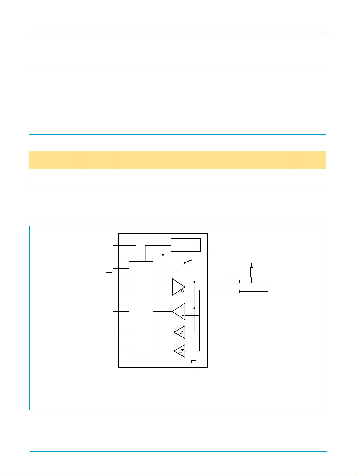
5. Functional diagram
handbook, full pagewidth
V
CC(I/O)
SOFTCON
OE
FSE0
VO
SUSPND
RCV
VP
VM
LEVEL
SHIFTER
3.3 V
ISP1107
VOLTAGE
REGULATOR
GND
V
CC(5.0)
V
reg(3.3)
V
pu(3.3)
D+
D−
MGS962
33 Ω
33 Ω
(1)
(1)
(1%)
(1%)
1.5 kΩ
(2)
(1) Use a 39 Ω resistor (1%) for a USB v2.0 compliant output impedance range.
(2) Connect to D− for low-speed operation.
Fig 1. Functional diagram.
9397 750 06899
Objective specification Rev. 01 — 23 February 2000 2 of 19
© Philips Electronics N.V. 2000. All rights reserved.
Philips Semiconductors
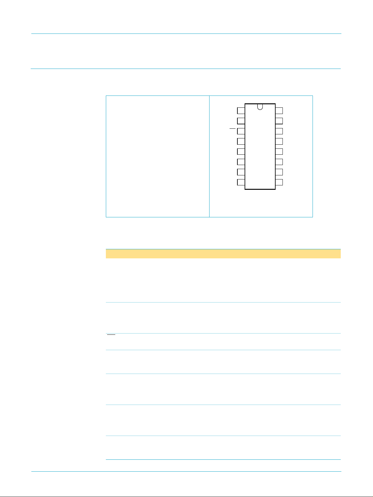
6. Pinning information
6.1 Pinning
ISP1107
Advanced USB transceiver
page
Fig 2. Pinning diagram BCC16
V
SOFTCON
SUSPND
Fig 3. Pinning diagram TSSOP16.
pu(3.3)
OE
RCV
VP
VM
GND
1
2
3
4
ISP1107DH
5
6
7
8
16
15
14
13
12
11
10
9
MGS961
(to be added).
6.2 Pin description
Table 2: Pin description
Symbol Pin Type Description
V
pu(3.3)
SOFTCON 2 I software controlled USB connection input; a HIGH level
OE 3 I output enable input (CMOS level re. V
RCV 4 O differential data receiver output (CMOS level re. V
VP 5 O single-ended D+ receiver output (CMOS level re. V
VM 6 O single-ended D− receiver output (CMOS level re. V
SUSPND 7 I suspend input (CMOSlevel re.V
1 - pull-up supply voltage (3.3 V ± 10%); used to connect an
external 1.5 kΩ resistor on D+ (full-speed) or D− (low-speed);
pin function is controlled by input SOFTCON:
SOFTCON = LOW — V
SOFTCON = HIGH — V
applies 3.3 V to pin V
pu(3.3)
floating (high impedance)
pu(3.3)
= 3.3 V
pu(3.3)
, which is connected to an external
1.5 kΩ pull-up resistor; this allows USB connect/disconnect
signalling to be controlled by software
enables the transceiver to transmit data on the USB bus
CC(I/O)
driven LOW when input SUSPND is HIGH; the output state of
RCV is preserved and stable during an SE0 condition
used for external detection of single-ended zero (SE0), error
conditions, speed of connected device; driven HIGH when
V
CC(5.0)/Vreg(3.3)
are not connected to any voltage supply
used for external detection of single-ended zero (SE0), error
conditions, speed of connected device; driven HIGH when no
supply voltage is connected to V
or V
CC(5.0)
); a HIGHlevel enables
CC(I/O)
low-power state while the USB bus is inactive and drives
output RCV to a LOW level
V
CC(5.0)
V
reg(3.3)
FSE0
VO
D+
D−
SPEED
V
CC(I/O)
, active LOW);
reg(3.3)
CC(I/O)
CC(I/O)
CC(I/O)
);
);
);
9397 750 06899
Objective specification Rev. 01 — 23 February 2000 3 of 19
© Philips Electronics N.V. 2000. All rights reserved.

Philips Semiconductors
ISP1107
Advanced USB transceiver
Table 2: Pin description
…continued
Symbol Pin Type Description
GND 8 - ground supply
V
CC(I/O)
9 - supply voltage for digital I/O pins (1.65 to 3.6 V). Three
voltage levels are supported: 1.8 V ± 0.15 V, 2.5 V ± 0.2 V
and 3.3 V ± 0.3V; when V
is not connected, the D+/D−
CC(I/O)
pins are in three-state
SPEED 10 I speed selection input (CMOS level re. V
CC(I/O)
); adjusts the
slew rate of differential data outputs D+ and D− according to
the transmission speed:
LOW: low-speed (1.5 Mbit/s)
HIGH: full-speed (12 Mbit/s)
D− 11 AI/O negative USB data bus connection (analog, differential); for
low-speed mode connect to pin V
via a 1.5 kΩ resistor
pu(3.3)
D+ 12 AI/O positive USB data bus connection (analog, differential); for
full-speed mode connect to pin V
VO 13 I differential driver data input (CMOS level re. V
via a 1.5 kΩ resistor
pu(3.3)
CC(I/O)
, Schmitt
trigger); see Table 4
FSE0 14 I differential driver data input (CMOS level re. V
CC(I/O)
, Schmitt
trigger); see Table 4
V
reg(3.3)
15 - regulated supply voltage output (3.0 to 3.6 V) during 5 V
operation; used as supply voltage input for 3.3 V operation
(3.3 V ± 10%)
V
CC(5.0)
16 - supply voltage for 5 V operation (4.0 to 5.5 V); can be
connected directly to USB supply V
during 3.3 V operation
V
reg(3.3)
; connect this pin to
BUS
7. Functional description
7.1 Function selection
Table 3: Function table
SUSPND OE D+/D− RCV VP/VM Function
L L driving &
receiving
L H receiving
H L driving inactive
H H high-Z
[1] Signal levels on D+/D− are determined by other USB devices and external pull-up/down resistors.
[2] In ‘suspend’ mode (SUSPND = HIGH) the differential receiver is inactive and output RCV is always
LOW. Out-of-suspend (‘K’) signalling is detected via the single-ended receivers VP and VM.
[3] During suspend, the slew-rate control circuit of low-speed operation is disabled. The D+/D− are still
driven to their intended states, without slew-rate control. This is permitted because driving during
suspend is used to signal remote wakeup by driving a ‘K’ signal (one transition from idle to ‘K’ state)
for a period of 1 to 15 ms.
9397 750 06899
Objective specification Rev. 01 — 23 February 2000 4 of 19
[1]
active active normal driving
(differential receiver active)
[1]
active active receiving
[2]
active driving during ‘suspend’
(differential receiver inactive)
inactive
[2]
active low-power state
© Philips Electronics N.V. 2000. All rights reserved.
[3]

Philips Semiconductors
7.2 Operating functions
Table 4: Driving function (OE = L)
ISP1107
Advanced USB transceiver
FSE0 VO Data
L L differential logic 0
L H differential logic 1
H L SE0
H H SE0
Table 5: Receiving function (
D+/D− RCV VP VM
differential logic 0 L L H
differential logic 1 H H L
SE0 RCV*
[1] RCV* denotes the signal level on output RCV just before SE0 state occurs. This level is kept stable
during the SE0 period.
OE=H)
[1]
LL
7.3 Power supply configurations
The ISP1107 can be used with different power supply configurations, which can be
changed dynamically. An overview is given in Table 6.
Normal mode — Both V
operation, V
is connected to a 5 V source (4.0 to 5.5 V). The internal voltage
CC(5.0)
regulator then produces 3.3 V for the USB connections. For 3.3 V operation, both
V
CC(5.0)
and V
are connected to a 3.3 V source (3.0 - 3.6 V). V
reg(3.3)
independently connected to a 1.8 V, 2.5 V or 3.3 V source, depending on the supply
voltage of the external circuit.
Disable mode — V
CC(I/O)
mode, the ISP1107’s internal circuits ensure that the D+/D− pins are in three-state
and the power consumption drops to the low-power (suspended) state level.
and V
CC(I/O)
CC(5.0)/Vreg(3.3)
is not connected, V
are connected. For 5 V
CC(5.0)/Vreg(3.3)
are connected. In this
CC(I/O)
is
Sharing mode — V
is connected, V
CC(I/O)
CC(5.0)/Vreg(3.3)
are not connected. In this
mode, the D+/D− pins are made three-state and the ISP1107 allows external signals
of up to 3.6 V to share the D+/D− lines. The ISP1107’s internal circuits ensure that
virtually no current is drawn via the D+/D− lines. The power consumption through pin
V
drops to the low-power (suspended) state level. Both the VP and VM pins are
CC(I/O)
driven HIGH to indicate this mode.
Table 6: Power supply configuration overview
V
CC(5.0)/Vreg(3.3)
connected connected Normal mode connected not connected Disable mode D+/D− high impedance
not connected connected Sharing mode D+/D− are high impedance;
9397 750 06899
Objective specification Rev. 01 — 23 February 2000 5 of 19
V
CC(I/O)
Configuration Special characteristics
VP/VM are driven HIGH
© Philips Electronics N.V. 2000. All rights reserved.

Philips Semiconductors
ISP1107
Advanced USB transceiver
8. Limiting values
Table 7: Absolute maximum ratings
In accordance with the Absolute Maximum Rating System (IEC 60134).
Symbol Parameter Conditions Min Max Unit
V
CC(5.0)
V
CC(I/O)
V
reg(3.3)
V
I
I
latchup
V
esd
T
stg
[1] Equivalent to discharging a 100 pF capacitor via a 1.5 kΩ resistor (Human Body Model).
supply voltage −0.5 +6.0 V
I/O supply voltage −0.5 +4.6 V
regulated supply voltage −0.5 +4.6 V
DC input voltage −0.5 V
CC(I/O)
+ 0.5 V
latchup current VI=−1.8 to 5.4 V - 100 mA
electrostatic discharge voltage
[1]
ILI<1µA
pins D+, D− - ±8000 V
other pins - ±2000 V
storage temperature −40 +125 °C
Table 8: Recommended operating conditions
Symbol Parameter Conditions Min Typ Max Unit
V
CC(5.0)
V
CC(I/O)
V
reg(3.3)
V
I
V
I(AI/O)
supply voltage 5 V operation 4.0 5.0 5.5 V
I/O supply voltage 1.65 - 3.6 V
regulated supply voltage 3.3 V operation 3.0 3.3 3.6 V
input voltage 0 - V
input voltage on analog I/O
0 - 3.6 V
CC(I/O)
V
pins (D+/D−)
T
amb
operating ambient temperature −40 - +85 °C
9397 750 06899
Objective specification Rev. 01 — 23 February 2000 6 of 19
© Philips Electronics N.V. 2000. All rights reserved.
 Loading...